


查询HT46C22供应商
Features
·
Operating voltage:
f
=4MHz: 2.2V~5.5V
SYS
f
=8MHz: 4.5V~5.5V
SYS
·
19 bidirectional I/O lines (max.)
·
1 interrupt input shared with an I/O line
·
8-bit programmable timer/event counter with over
flow interrupt and 7-stage prescaler
·
On-chip crystal and RC oscillator
·
Watchdog Timer
·
2048´14 program memory ROM
·
64´8 data memory RAM
·
Supports PFD for sound generation
·
HALT function and wake-up feature reduce power
consumption
General Description
The device is an 8-bit high performance RISC-like
microcontroller designed for multiple I/O product appli
cations. It is particularly suitable for use in products
HT46R22/HT46C22
8-Bit A/D Type MCU
·
Up to 0.5ms instruction cycle with 8MHz system clock
at V
=5V
DD
·
6-level subroutine nesting
·
8 channels 9-bit resolution (8-bit accuracy) A/D con
verter
·
-
-
1-channel (6+2)/(7+1)-bit PWM output shared with
two I/O lines
·
Bit manipulation instruction
·
14-bit table read instruction
·
63 powerful instructions
·
All instructions in one or two machine cycles
·
Low voltage reset function
·
I2C BUS (slave mode)
·
24-pin SKDIP/SOP package
such as washing machine controllers and home appli
ances. A HALT feature is included to reduce power con
sumption.
-
-
-
I2C is a trademark of Philips Semiconductors
Rev. 1.10 1 October 2, 2002
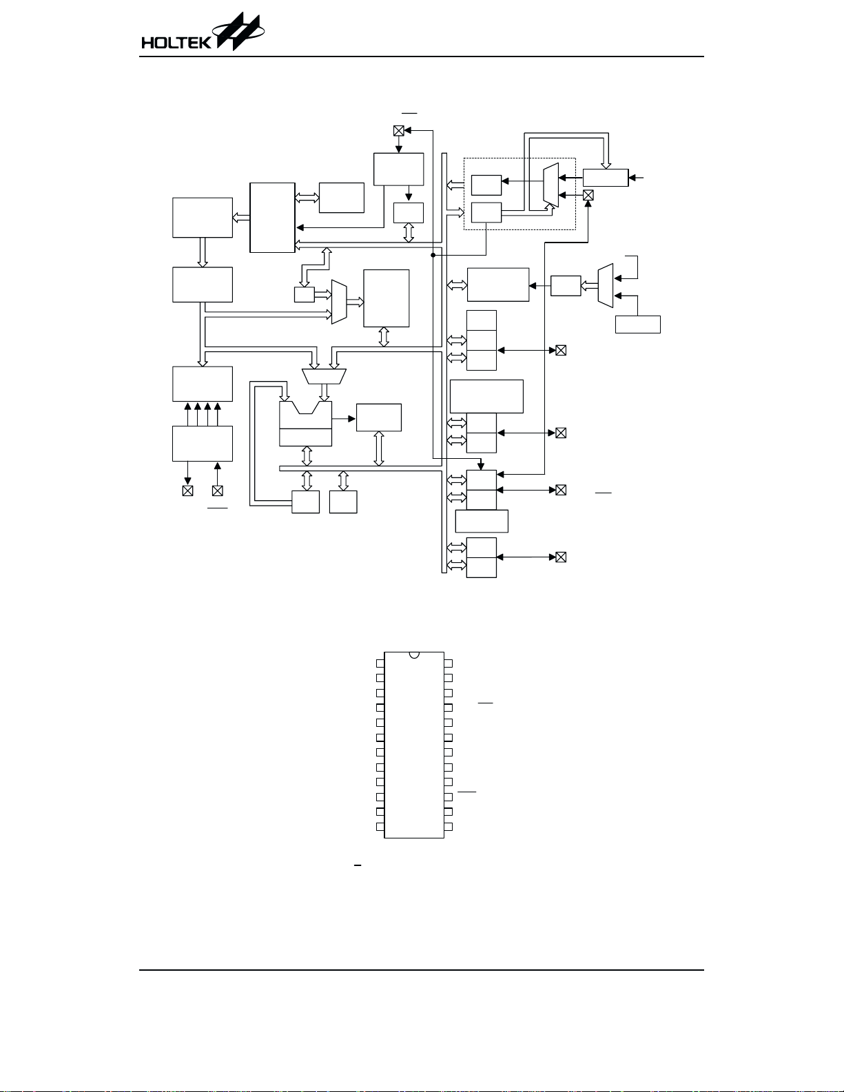
Block Diagram
HT46R22/HT46C22
P A 5 / I N T
P r o g r a m
R O M
I n s t r u c t i o n
R e g i s t e r
I n s t r u c t i o n
D e c o d e r
T i m i n g
G e n e r a t o r
O S C 2 O S C 1
R E S
V D D
V S S
P r o g r a m
C o u n t e r
M P
A L U
S h i f t e r
A C C
M U X
S T A C K
M
U
X
L V R
D A T A
M e m o r y
S T A T U S
I n t e r r u p t
C i r c u i t
I N T C
P A 3 , P A 5
T M R
T M R C
P A 3 / P F D
W D T
P r e s c a l e r
P W M
P O R T D
P D C
P D
8 - C h a n n e l
A / D C o n v e r t e r
P B C
P O R T B
P B
P A C
P A
2
I C B U S
S l a v e M o d e
P C
P C C
P O R T A
M
P r e s c a l e r
U
X
W D T
P A 4 / T M R
P A 4
S Y S C L K / 4
P D 0 / P W M
P B 0 / A N 0 ~ P B 7 / A N 7
P A 0 ~ P A 2
P A 3 / P F D
P A 4 / T M R
P A 5 / I N T
P A 6 / S D A
P A 7 / S C L
P C 0 ~ P C 1
M
U
X
R C O S C
f
S Y S
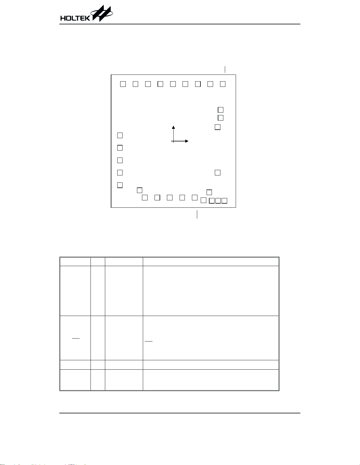
Pin Assignment
P B 5 / A N 5
P B 4 / A N 4
P A 3 / P F D
P B 3 / A N 3
P B 2 / A N 2
P B 1 / A N 1
P B 0 / A N 0
Rev. 1.10 2 October 2, 2002
P A 2
P A 1
P A 0
V S S
P C 0
1
2
3
4
5
6
7
8
9
1 0
1 1
1 2
2 4
2 3
2 2
2 1
2 0
1 9
1 8
1 7
1 6
1 5
1 4
1 3
H T 4 6 R 2 2 / H T 4 6 C 2 2
2 4 S K D I P - A / S O P - A
P B 6 / A N 6
P B 7 / A N 7
P A 4 / T M R
P A 5 / I N T
P A 6 / S D A
P A 7 / S C L
O S C 2
O S C 1
V D D
R E S
P D 0 / P W M
P C 1
Pad Assignment
HT46C22
HT46R22/HT46C22
P A 3 / P F D
P B 4 / A N 4
P A 2
P B 6 / A N 6
P B 5 / A N 5
P A 4 / T M R
P B 7 / A N 7
P A 5 / I N T
P A 1
P A 0
P B 3 / A N 3
P B 2 / A N 2
P B 1 / A N 1
P B 0 / A N 0
2 8
V S S
8
V S S
2 7
9
P C 0
1
2 9
2
3
4
5
6
7
2 5
1 1 1 2
P D 0 / P W M
2 4
2 3
1 5
1 3
1 4
R E S
V D D
2 6
( 0 , 0 )
1 0
P C 1
* The IC substrate should be connected to VSS in the PCB layout artwork.
Pad Description
Pad Name I/O Options Description
PB0/AN0
PB1/AN1
PB2/AN2
PB3/AN3
PB4/AN4
I/O Pull-high
PB5/AN5
PB6/AN6
PB7/AN7
PA0~PA2
PA3/PFD
PA4/TMR
PA5/INT
PA6/SDA
I/O
Pull-high
Wake-up
PA3 or PFD
I/O or Serial Bus
PA7/SCL
VSS
¾¾
PC0~PC1 I/O Pull-high
Bidirectional 8-bit input/output port. Software instructions deter
mine the CMOS output, Schmitt trigger input with or without
pull-high resistor (determined by pull-high option: port option) or
A/D input.
Once a PB line is selected as an A/D input (by using software
control), the I/O function and pull-high resistor are disabled auto
matically.
Bidirectional 8-bit input/output port. Each bit can be configured as
wake-up input by options. Software instructions determine the
CMOS output or Schmitt trigger input with or without pull-high resis
tor (determined by pull-high options: bit option). The PFD, TMR and
INT
are pin-shared with PA3, PA4 and PA5, respectively. Once
2
the I
C BUS function is used, the internal registers related to PA6
and PA7 can not be used.
Negative power supply, ground.
Bidirectional 2-bit input/output port. Software instructions deter
mine the CMOS output, Schmitt trigger input with or without
pull-high resistor (determine by pull-high option: port option).
2 2
2 1
2 0
1 9
1 8
V D D
1 6
T E S T 1
T E S T 2
P A 6 / S D A
P A 7 / S C L
O S C 2
O S C 1
1 7
T E S T 3
-
-
-
-
Rev. 1.10 3 October 2, 2002
HT46R22/HT46C22
Pad Name I/O Options Description
Bidirectional 1-bit input/output port. Software instructions deter
mine the CMOS output, Schmitt trigger input with or without a
pull-high resistor (determined by pull-high option: port option).
The PWM output function is pin-shared with PD0 (dependent on
PD0/PWM I/O
Pull-high
I/O or PWM
PWM optios).
RES
VDD
OSC1
OSC2
TEST1
TEST2
TEST3
I
¾
¾¾
I
Crystal or RC
O
I
¾
Schmitt trigger reset input. Active low.
Positive power supply
OSC1, OSC2 are connected to an RC network or a Crystal (de
termined by options) for the internal system clock. In the case of
RC operation, OSC2 is the output terminal for 1/4 system clock.
TEST mode input pin
It disconnects in normal operation
Absolute Maximum Ratings
Supply Voltage...........................VSS-0.3V to VSS+5.5V
Input Voltage..............................V
-0.3V to VDD+0.3V
SS
Note: These are stress ratings only. Stresses exceeding the range specified under ²Absolute Maximum Ratings² may
cause substantial damage to the device. Functional operation of this device at other conditions beyond those
listed in the specification is not implied and prolonged exposure to extreme conditions may affect device reliabil
ity.
Storage Temperature ............................-50°Cto125°C
Operating Temperature...........................-40°Cto85°C
-
-
-
D.C. Characteristics
Symbol Parameter
V
V
I
DD1
I
DD2
I
DD3
I
ADC
I
STB1
I
STB2
V
V
DD1
DD2
AD
IL1
Operating Voltage
Operating Voltage
Operating Current (Crystal OSC)
Operating Current (RC OSC)
Operating Current 5V
Only ADC Enable, Others Disable
Standby Current (WDT Enabled)
Standby Current (WDT Disabled)
A/D Input Voltage
Input Low Voltage for I/O Ports,
TMR and INT
Test Conditions
V
DD
¾
¾
3V
5V
3V
5V
Conditions
=4MHz
f
SYS
=8MHz
f
SYS
No load, f
SYS
ADC disable
No load, f
SYS
ADC disable
No load, f
SYS
=4MHz
=4MHz
=8MHz
ADC disable
3V
No load
5V
3V
No load, system HALT
5V
3V
No load, system HALT
5V
¾¾
3V
5V
¾
¾
Ta=25°C
Min. Typ. Max. Unit
2.2
4.5
0.6 1.5 mA
¾
¾
0.8 1.5 mA
¾
2.5 4 mA
¾
¾
0.5 1 mA
¾
1.5 3 mA
¾
¾¾
¾¾
¾¾
¾¾
0
0
0
5.5 V
¾
5.5 V
¾
24mA
35mA
5
mA
¾
¾
¾
10
V
0.3V
0.3 V
1
2
DD
DD
mA
mA
mA
V
V
Rev. 1.10 4 October 2, 2002
HT46R22/HT46C22
Symbol Parameter
V
IH1
V
IL2
V
IH2
V
LVR
I
OL
I
OH
R
PH
E
AD
Input High Voltage for I/O Ports,
TMR and INT
Input Low Voltage (RES)
Input High Voltage (RES)
Low Voltage Reset
I/O Port Sink Current
I/O Port Source Current
Pull-high Resistance
A/D Conversion Error
A.C. Characteristics
Symbol Parameter
f
SYS1
f
SYS2
f
TIMER
t
AD
t
ADC
t
WDTOSC
t
RES
t
SST
t
INT
t
IIC
t
OPT
Note: *t
System Clock (Crystal OSC)
System Clock (RC OSC)
Timer I/P Frequency (TMR)
A/D Clock Period 5V
A/D Conversion Time
Watchdog Oscillator
External Reset Low Pulse Width
System Start-up Timer Period
Interrupt Pulse Width
I2C BUS Clock Period
Option Load Time During Reset
=1/f
SYS
SYS
Test Conditions
V
DD
3V
5V
3V
5V
3V
5V
Conditions
¾
¾
¾
¾
¾
¾
¾¾
=0.1V
V
3V
OL
DD
=0.1V
V
5V
OL
DD
V
3V
5V
3V
5V
=0.9V
OH
V
OH
=0.9V
DD
DD
¾
¾
¾¾ ¾±0.5 ±1
Min. Typ. Max. Unit
0.7V
0.7V
0.9V
0.9V
DD
DD
0
0
DD
DD
V
¾
¾
¾
¾
¾
¾
V
0.4V
0.4V
V
V
DD
DD
DD
DD
DD
DD
2.7 3 3.3 V
48
10 20
¾
¾
-2 -4 ¾
-5 -10 ¾
40 60 80
10 30 50
LSB
Ta=25°C
Test Conditions
V
DD
3V
5V
3V
5V
3V
5V
Conditions
¾
¾
¾
¾
¾
¾
¾
Min. Typ. Max. Unit
400
400
400
400
0
0
1
4000 kHz
¾
8000 kHz
¾
4000 kHz
¾
8000 kHz
¾
4000 kHz
¾
8000 kHz
¾
¾¾ms
¾¾ ¾76¾
3V
5V
¾
¾
¾¾
Wake-up from HALT
¾
¾¾
Connect to external
¾
pull-high resistor 2kW
3V System power on, WDT
time-out at normal mode,
5V 35 70 140 ms
RES
is reset
43 86 168
35 65 130
1
¾¾ms
*t
¾
*t
64
1024
¾
1
¾¾ms
¾¾
45 90 180 ms
V
V
V
V
V
V
mA
mA
mA
mA
kW
kW
t
AD
ms
ms
SYS
SYS
Rev. 1.10 5 October 2, 2002
Functional Description
Execution flow
The system clock for the microcontroller is derived from
either a crystal or an RC oscillator. The system clock is
internally divided into four non-overlapping clocks. One
instruction cycle consists of four system clock cycles.
Instruction fetching and execution are pipelined in such
a way that a fetch takes an instruction cycle while de
coding and execution takes the next instruction cycle.
However, the pipelining scheme causes each instruc
tion to effectively execute in a cycle. If an instruction
changes theprogram counter, two cyclesare required to
complete the instruction.
Program counter - PC
The program counter (PC) controls the sequence in
which the instructions stored in program ROM are exe
cuted and its contents specify full range of program
memory.
After accessing a program memory word to fetch an in
struction code, the contents of the program counter are in
HT46R22/HT46C22
cremented by 1. The program counter then points to the
memory word containing the next instruction code.
When executing a jump instruction, conditional skip ex
ecution, loading PCL register, subroutine call, initial re
set, internal interrupt, external interrupt or return from
subroutine, the PC manipulates the program transfer by
loading the address corresponding to each instruction.
-
The conditional skip is activated by instructions. Once
-
the condition is met, the next instruction, fetched during
the current instruction execution, is discarded and a
dummy cycle replaces it to get the proper instruction.
Otherwise proceed with the next instruction.
The lower byte of the program counter (PCL) is a read
able and writeable register (06H). Moving data into the
PCL performs a short jump. The destination will be
within 256 locations.
When a control transfer takes place, an additional
dummy cycle is required.
-
-
-
-
-
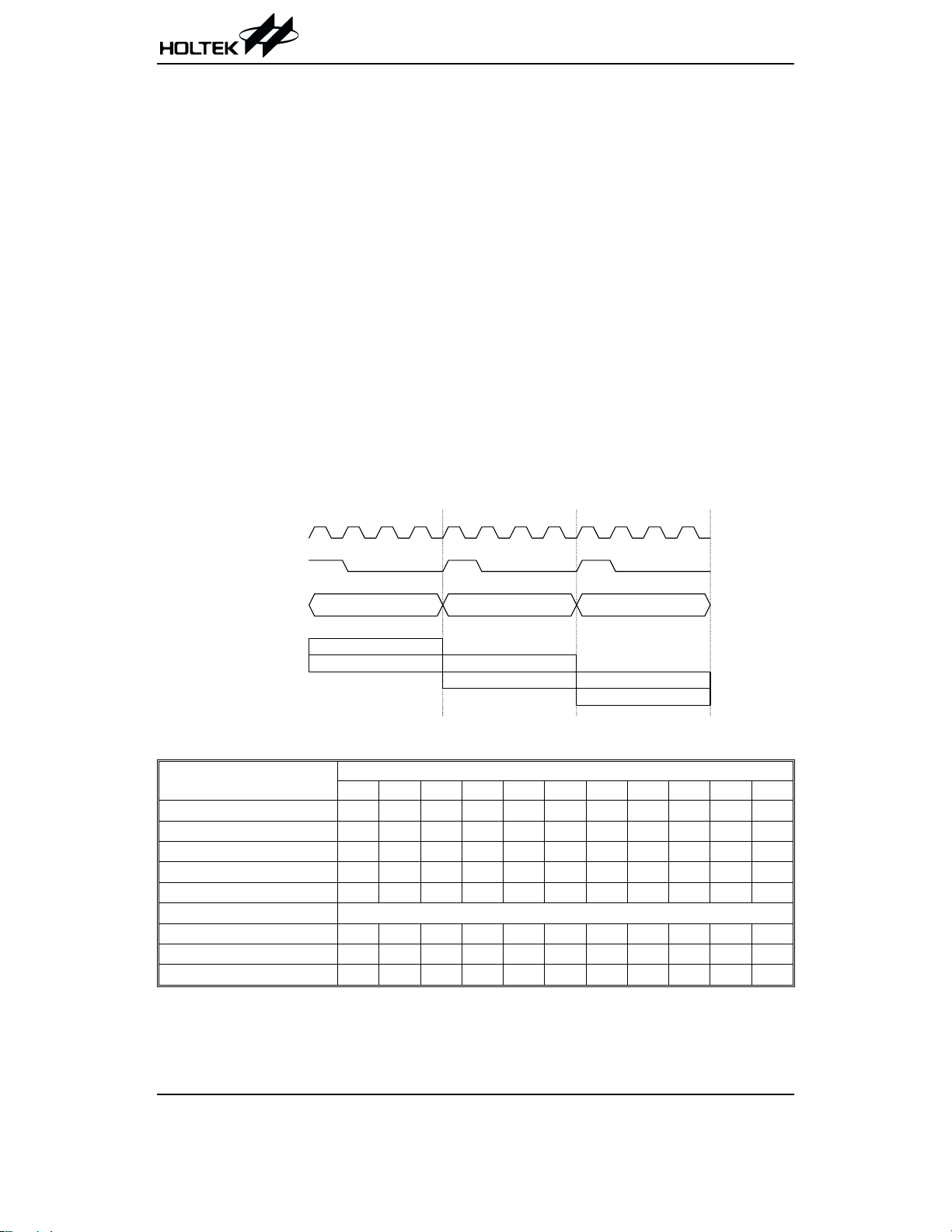
S y s t e m C l o c k
O S C 2 ( R C o n l y )
T 1 T 2 T 3 T 4 T 1 T 2 T 3 T 4 T 1 T 2 T 3 T 4
P C
P C P C + 1 P C + 2
F e t c h I N S T ( P C )
E x e c u t e I N S T ( P C - 1 )
F e t c h I N S T ( P C + 1 )
E x e c u t e I N S T ( P C )
F e t c h I N S T ( P C + 2 )
E x e c u t e I N S T ( P C + 1 )
Execution flow
Mode
*10 *9 *8 *7 *6 *5 *4 *3 *2 *1 *0
Program Counter
Initial Reset 00000000000
External Interrupt 00000000100
Timer/Event Counter Overflow 00000001000
A/D Converter Interrupt 00000001100
2
I
C BUS Interrupt 00000010000
Skip PC+2
Loading PCL *10 *9 *8 @7 @6 @5 @4 @3 @2 @1 @0
Jump, Call Branch #10 #9 #8 #7 #6 #5 #4 #3 #2 #1 #0
Return from Subroutine S10 S9 S8 S7 S6 S5 S4 S3 S2 S1 S0
Program counter
Note: *10~*0: Program counter bits S10~S0: Stack register bits
#10~#0: Instruction code bits @7~@0: PCL bits
Rev. 1.10 6 October 2, 2002
Program memory - ROM
The program memory is used to store the program in
structions which are to be executed. It also contains
data, table, and interrupt entries, and is organized into
2048´14 bits,addressed by the program counter and ta
ble pointer.
Certain locations in the program memory are reserved
for special usage:
·
Location 000H
This area is reserved for program initialization. After
chip reset, the program always begins execution at lo
cation 000H.
·
Location 004H
This area is reserved for the external interrupt service
program. If the INT
input pin is activated, the interrupt
is enabled and the stack is not full, the program begins
execution at location 004H.
·
Location 008H
This area is reserved for the timer/event counter inter
rupt service program. If a timer interrupt results from a
timer/event counter overflow, and if the interrupt is en
abled and the stack is not full, the program begins exe
cution at location 008H.
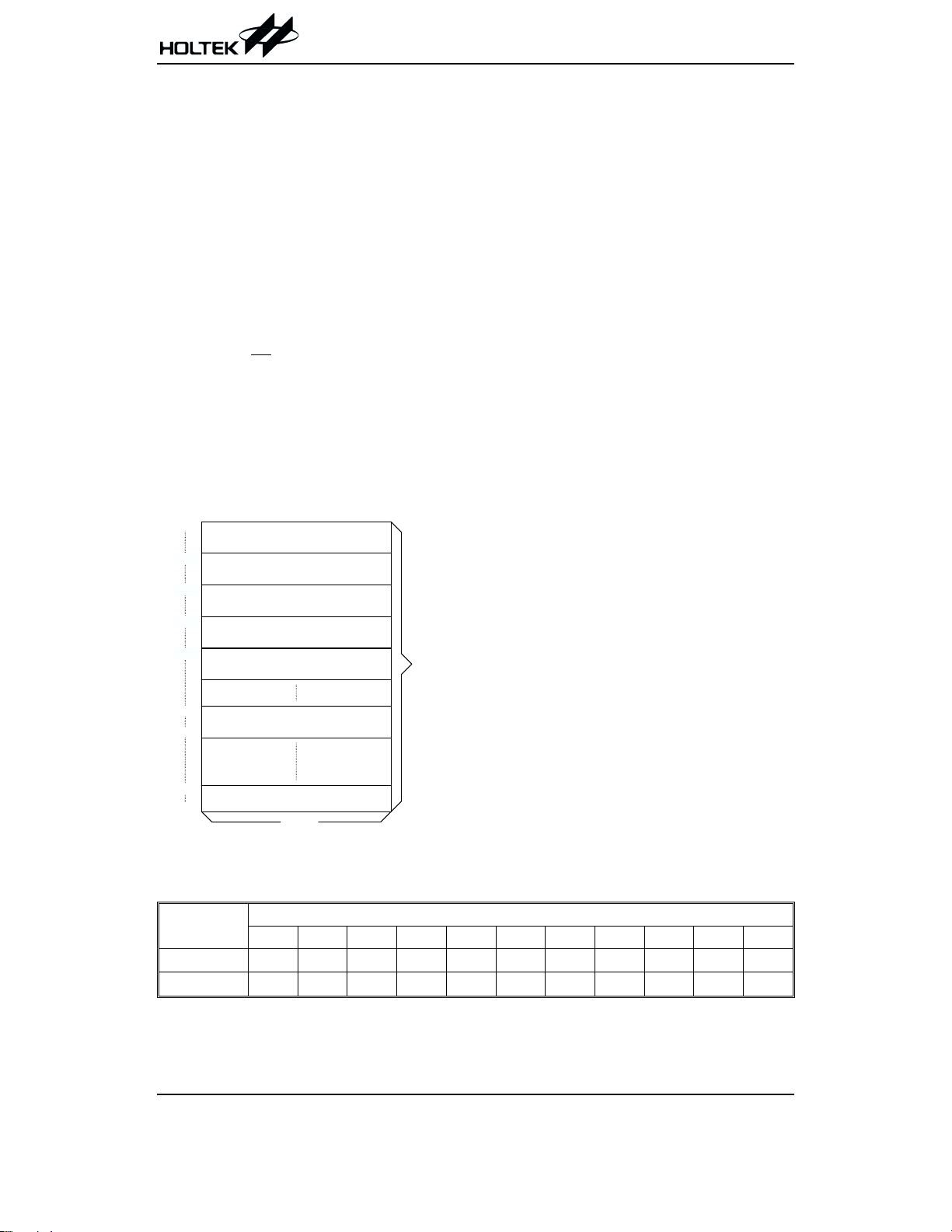
0 0 0 H
0 0 4 H
0 0 8 H
0 0 C H
0 1 0 H
n 0 0 H
n F F H
7 0 0 H
7 F F H
D e v i c e I n i t i a l i z a t i o n P r o g r a m
E x t e r n a l I n t e r r u p t S u b r o u t i n e
T i m e r / E v e n t C o u n t e r I n t e r r u p t S u b r o u t i n e
A / D C o n v e r t e r I n t e r r u p t S u b r o u t i n e
H - B U S I n t e r r u p t S u b r o u t i n e
L o o k - u p T a b l e ( 2 5 6 w o r d s )
L o o k - u p T a b l e ( 2 5 6 w o r d s )
1 4 b i t s
N o t e : n r a n g e s f r o m 0 t o 7
P r o g r a m
M e m o r y
HT46R22/HT46C22
·
Location 00CH
-
-
-
-
-
-
This area is reserved for the A/D converter interrupt
service program. If an A/D converter interrupt results
from an end of A/D conversion, and if the interrupt is
enabled and the stack is not full, the program begins
execution at location 00CH.
·
Location 010H
This area is reserved for the I
program. If the I
2
C BUS interrupt resulting from a
2
C BUS interrupt service
slave address is match or completed 1 byte of data
transfer, and if the interrupt is enable and the stack is
not full, the program begins execution at location
010H.
·
Table location
Any location in the ROM space can be used as
look-up tables. The instructions ²TABRDC [m]² (the
current page, 1 page=256 words) and ²TABRDL [m]²
(the last page) transfer the contents of the lower-order
byte to the specified data memory, and the
higher-order byte to TBLH (08H). Only the destination
of the lower-order byte in the table is well-defined, the
other bits of the table word are transferred to the lower
portion of TBLH, and the remaining 2 bit is read as ²0².
The Table Higher-order byte register (TBLH) is read
only. The table pointer (TBLP) is a read/write register
(07H), which indicates the table location. Before accessing the table, the location must be placed in
TBLP. The TBLH is read only and cannot be restored.
If the main routine and the ISR (Interrupt Service Routine) both employ the table read instruction, the contents of the TBLH in the main routine are likely to be
changed by the table read instruction used in the ISR.
Errors can occur. In other words, using the table read
instruction in the main routine and the ISR simultaneously should be avoided. However, if the table read
instruction has to be applied in both the main routine
and the ISR, the interrupt is supposed to be disabled
prior to the table read instruction. It will not be enabled
until the TBLH has been backed up. All table related
instructions require two cycles to complete the opera
tion. These areas may function as normal program
memory depending upon the requirements.
-
Program memory
Instruction
*10 *9 *8 *7 *6 *5 *4 *3 *2 *1 *0
Table Location
TABRDC [m] P10 P9 P8 @7 @6 @5 @4 @3 @2 @1 @0
TABRDL [m] 1 1 1 @7 @6 @5 @4 @3 @2 @1 @0
Table location
Note: *10~*0: Table location bits P10~P8: Current program counter bits
@7~@0: Table pointer bits
Rev. 1.10 7 October 2, 2002
HT46R22/HT46C22
Stack register - STACK
This is a special part of the memory which is used to
save the contents of the program counter (PC) only. The
stack is organized into 6 levels and is neither part of the
data nor part of the program space, and is neither read
able nor writeable. The activated level is indexed by the
stack pointer (SP) and is neither readable nor writeable.
At a subroutine call or interrupt acknowledgment, the
contents of the program counter are pushed onto the
stack. At the end of a subroutine or an interrupt routine,
signaled by a return instruction (RET or RETI), the pro
gram counter is restored to its previous value from the
stack. Aftera chip reset, the SP will point to the top of the
stack.
If the stack is full and a non-masked interrupt takes
place, the interrupt request flag will be recorded but the
acknowledgment will be inhibited. When the stack
pointer is decremented (by RET or RETI), the interrupt
will be serviced. This feature prevents stack overflow al
lowing the programmer to use the structure more easily.
In a similar case, if the stack is full and a ²CALL² is sub
sequently executed, stack overflow occurs and the first
entry will be lost (only the most recent 6 return ad
dresses are stored).
Data memory - RAM
The data memory is designed with 92´8 bits. The data
memory is divided into two functional groups: special
function registers and general purpose data memory
(64´8). Most are read/write, but some are read only.
The special function registers include the indirect addressing register (00H), timer/event counter register
(TMR;0DH), timer/event counter control register
(TMRC;0EH), program counter lower-order byte regis
ter (PCL;06H), memory pointer register (MP;01H), ac
cumulator (ACC;05H), table pointer (TBLP;07H), table
higher-order byte register (TBLH;08H), status register
(STATUS;0AH), interrupt control register 0 (INTC0;
0BH), PWM data register (PWM;1AH), the I
slave address register (HADR;20H), the I
trol register (HCR;21H), the I
(HSR;22H), the I
2
C BUS data register (HDR;23H), the
2
C BUS status register
2
C BUS
2
C BUS con
A/D result lower-order byte register (ADRL;24H), the
A/D result higher-order byte register (ADRH;25H), the
A/D control register (ADCR;26H), the A/D clock setting
register (ACSR;27H), I/O registers (PA;12H, PB;14H,
PC;16H, PD;18H) and I/O control registers (PAC;13H,
PBC;15H, PCC;17H, PDC;19H). The remaining space
before the 40H is reserved for future expanded usage
and reading these locations will get ²00H². The general
purpose data memory, addressed from 40H to 7FH, is
used for data and control information under instruction
commands.
I n d i r e c t A d d r e s s i n g R e g i s t e r
0 0 H
0 1 H
0 2 H
0 3 H
0 4 H
-
0 5 H
0 6 H
0 7 H
0 8 H
0 9 H
0 A H
-
0 B H
0 C H
0 D H
0 E H
0 F H
1 0 H
1 1 H
1 2 H
1 3 H
-
1 4 H
1 5 H
-
1 6 H
1 7 H
1 8 H
-
1 9 H
1 A H
1 B H
1 C H
1 D H
1 E H
1 F H
2 0 H
2 1 H
2 2 H
2 3 H
2 4 H
-
2 5 H
-
2 6 H
2 7 H
2 8 H
-
3 F H
4 0 H
7 F H
M P
A C C
P C L
T B L P
T B L H
S T A T U S
I N T C 0
T M R
T M R C
P A
P A C
P B
P B C
P C
P C C
P D
P D C
P W M
I N T C 1
H A D R
H C R
H S R
H D R
A D R L
A D R H
A D C R
A C S R
G e n e r a l P u r p o s e
D A T A M E M O R Y
( 6 4 B y t e s )
R e a d a s " 0 0 "
RAM mapping
All of the data memory areas can handle arithmetic,
logic, increment, decrement and rotate operations di
rectly. Except for some dedicated bits, each bit in the
data memory can be set and reset by ²SET [m].i² and
²CLR [m].i². They are also indirectly accessible through
memory pointer register (MP;01H).
S p e c i a l P u r p o s e
D A T A M E M O R Y
: U n u s e d
-
Rev. 1.10 8 October 2, 2002
HT46R22/HT46C22
Indirect addressing register
Location 00H is an indirect addressing register that is
not physically implemented. Any read/write operation of
[00H] accesses data memory pointed to by MP (01H).
Reading location 00H itself indirectly will return the re
sult 00H. Writing indirectly results in no operation.
The memory pointer register MP (01H) is a 7-bit register.
The bit 7 of MP is undefined and reading will return the
result ²1². Any writing operation to MP will only transfer
the lower 7-bit data to MP.
Accumulator
The accumulator is closely related to ALU operations. It
is also mapped to location 05H of the data memory and
can carry out immediate data operations. The data
movement between two data memory locations must
pass through the accumulator.
Arithmetic and logic unit - ALU
This circuit performs 8-bit arithmetic and logic operations.
The ALU provides the following functions:
·
Arithmetic operations (ADD, ADC, SUB, SBC, DAA)
·
Logic operations (AND, OR, XOR, CPL)
·
Rotation (RL, RR, RLC, RRC)
·
Increment and Decrement (INC, DEC)
·
Branch decision (SZ, SNZ, SIZ, SDZ ....)
The ALU not only saves the results of a data operation but
also changes the status register.
Status register - STATUS
This 8-bit register (0AH) contains the 0 flag (Z), carry
flag (C), auxiliary carry flag (AC), overflow flag (OV),
power down flag (PD), and watchdog time-out flag (TO).
It also records the status information and controls the
operation sequence.
With the exception of the TO and PD flags, bits in the
status register can be altered by instructions like
most other registers. Any data written into the status
register will not change the TO or PD flag. In addition
operations related to the status register may give dif
ferent results from those intended. The TO flag can
be affected only by system power-up, a WDT
-
time-out or executing the ²CLR WDT² or ²HALT² in
struction. The PD flag can be affected only by exe
cuting the ²HALT² or ²CLR WDT² instruction or a
system power-up.
The Z, OV, AC and C flags generally reflect the status of
the latest operations.
In addition, on entering the interrupt sequence or exe
cuting the subroutine call, the status register will not be
pushed onto the stack automatically. If the contents of
the status are important and if the subroutine can cor
rupt the status register, precautions must be taken to
save it properly.
Interrupt
The device provides an external interrupt, an internal
timer/event counterinterrupt, the A/D converter interrupt
2
and the I
C BUS interrupts. The interrupt control register
0 (INTC0;0BH) and interrupt control register 1
(INTC1;1EH) contains the interrupt control bits to set the
enable or disable and the interrupt request flags.
Once an interrupt subroutine is serviced, all the other interrupts will be blocked (by clearing the EMI bit). This
scheme may prevent any further interrupt nesting. Other
interrupt requests may happen during this interval but
only the interrupt request flag is recorded. If a certain interrupt requires servicing within the service routine, the
EMI bit and the corresponding bit of INTC0 and INTC1
may be set to allow interrupt nesting. If the stack is full,
the interrupt request will not be acknowledged, even if the
related interrupt is enabled, until the SP is decremented.
If immediate service is desired, the stack must be pre
vented from becoming full.
-
-
-
-
-
-
Labels Bits Function
C is set if the operation results in a carry during an addition operation or if a borrow does not take
C0
place during a subtraction operation; otherwise C is cleared. C is also affected by a rotate
through carry instruction.
AC 1
AC is set if the operation results in a carry out of the low nibbles in addition or no borrow from the
high nibble into the low nibble in subtraction; otherwise AC is cleared.
Z 2 Z is set if the result of an arithmetic or logic operation is 0; otherwise Z is cleared.
OV 3
PD 4
TO 5
¾
OV is set if the operation results in a carry into the highest-order bit but not a carry out of the
highest-order bit, or vice versa; otherwise OV is cleared.
PD is cleared by system power-up or executing the ²CLR WDT² instruction. PD is set by execut
ing the ²HALT² instruction.
TO is cleared by system power-up or executing the ²CLR WDT² or ²HALT² instruction. TO is set
by a WDT time-out.
6, 7
Unused bit, read as ²0²
Status register
Rev. 1.10 9 October 2, 2002
-
HT46R22/HT46C22
All these kinds of interrupts have a wake-up capability.
As an interrupt is serviced, a control transfer occurs by
pushing the program counter onto the stack, followed by
a branch to a subroutine at specified location in the pro
gram memory. Only the program counter is pushed onto
the stack. If the contents of the register or status register
(STATUS) are altered by the interrupt service program
which corrupts the desired control sequence, the con
tents should be saved in advance.
External interrupts are triggered by a high to low transi
tion of INT
and the related interrupt request flag (EIF; bit
4 of INTC0) will be set. When the interrupt is enabled,
the stack is not full and the external interrupt is active, a
subroutine call to location 04H will occur. The interrupt
request flag (EIF) and EMI bits will be cleared to disable
other interrupts.
The internal timer/event counter interrupt is initialized by
setting the timer/event counter interrupt request flag
(TF; bit 5 of INTC0), caused by a timer overflow. When
the interrupt is enabled, the stack is not full and the TF
bit is set, a subroutine call to location 08H will occur. The
related interrupt request flag (TF) will be reset and the
EMI bit cleared to disable further interrupts.
The A/D converter interrupt is initialized by setting the
A/D converter request flag (ADF; bit 6 of INTC0),
caused by an end of A/D conversion. When the interrupt
is enabled, the stack is not full and the ADF is set, a subroutine call to location 0CH will occur. The related interrupt request flag (ADF) will be reset and the EMI bit
cleared to disable further interrupts.
Register Bit No. Label Function
Controls the master (global)
0 EMI
interrupt
(1= enabled; 0= disabled)
1 EEI
Controls the external interrupt
(1= enabled; 0= disabled)
Controls the timer/event
2 ETI
counter interrupt
(1= enabled; 0= disabled)
INTC0
(0BH)
3 EADI
4 EIF
Controls the A/D converter
interrupt
(1= enabled; 0= disabled)
External interrupt request flag
(1= active; 0= inactive)
Internal timer/event counter
5TF
request flag
(1= active; 0= inactive)
6 ADF
7
A/D converter request flag
(1= active; 0= inactive)
¾ Unused bit, read as ²0²
INTC0 register
2
C BUS interrupt is initialized by setting the I2C
The I
BUS interrupt request flag (HIF; bit 4 of INTC1), caused
by a slave address match (HAAS=²1²) or 1 byte of data
transfer is completed. When the interrupt is enabled, the
stack is not full and the HIF bit is set, a subroutine call to lo
cation 10H will occur. The related interrupt request flag
(HIF) will be reset and the EMI bit cleared to disable further
interrupts.
During the execution of an interrupt subroutine, other in
terrupt acknowledgments are held until the ²RETI² in
struction is executed or the EMI bit and the related
interrupt control bit are set to 1 (of course, if the stack is
-
not full). To return from the interrupt subroutine, ²RET² or
²RETI² may be invoked. RETI will set the EMI bit to en
able an interrupt service, but RET will not.
Interrupts, occurring in the interval between the rising
edges of two consecutive T2 pulses, will be serviced on
the latter of the two T2 pulses, if the corresponding inter
rupts are enabled. In the case of simultaneous requests
the following table shows the priority that is applied.
These can be masked by resetting the EMI bit.
No. Interrupt Source Priority Vector
a External Interrupt 1 04H
b Timer/Event Counter Overflow 2 08H
c A/D Converter Interrupt 3 0CH
2
dI
C BUS Interrupt 4 10H
The timer/event counter interrupt request flag (TF), external interrupt request flag (EIF), A/D converter request
flag (ADF), the I
2
C BUS interrupt request flag (HIF), enable timer/event counter bit (ETI), enable external interrupt bit (EEI), enable A/D converter interrupt bit (EADI),
2
enable I
C BUS interrupt bit (EHI) and enable master interrupt bit (EMI) constitute an interrupt control register 0
(INTC0) and an interrupt control register 1 (INTC1)
which are located at 0BH and 1EH in the data memory.
EMI, EEI, ETI, EADI, EHI are used to control the en
abling/disabling of interrupts. These bits prevent the re
quested interrupt from being serviced. Once the
interrupt request flags (TF, EIF, ADF, HIF) are set, they
will remain in the INTC0 and INTC1 register until the in
terrupts are serviced or cleared by a software instruc
tion.
Register Bit No. Label Function
Controls the I
rupt (1=enabled;0=disabled)
¾ Unused bit, read as ²0²
¾ Unused bit, read as ²0²
¾ Unused bit, read as ²0²
2
I
C BUS interrupt request
flag (1=active; 0=inactive)
¾ Unused bit, read as ²0²
¾ Unused bit, read as ²0²
¾ Unused bit, read as ²0²
INTC1
(1EH)
0 EHI
1
2
3
4 HIF
5
6
7
INTC1 register
2
C BUS inter
-
-
-
-
-
-
-
-
-
-
Rev. 1.10 10 October 2, 2002
HT46R22/HT46C22
It is recommended that a program does not use the
²CALL subroutine² within the interrupt subroutine. In
terrupts often occur in an unpredictable manner or
need to be serviced immediately in some applications.
If only one stack is left and enabling the interrupt is not
well controlled, the original control sequence will be dam
aged once the ²CALL² operates in the interrupt subrou
tine.
Oscillator configuration
There are two oscillator circuits in the microcontroller.
V
D D
O S C 1
f
/ 4
O S C 2
C r y s t a l O s c i l l a t o r R C O s c i l l a t o r
S Y S
N M O S O p e n D r a i n
O S C 1
O S C 2
System oscillator
Both are designed for system clocks, namely the RC os
cillator and the Crystal oscillator, which are determined
by the options. No matter what oscillator type is se
lected, the signal provides the system clock. The HALT
mode stops the system oscillator and ignores an exter
nal signal to conserve power.
If an RC oscillator is used, an external resistor between
OSC1 and VSS is required and the resistance must
range from 30kW to 750kW. The system clock, divided
by 4, is available on OSC2, which can be used to synchronize external logic. The RC oscillator provides the
most cost effective solution. However, the frequency of
oscillation may vary with VDD, temperatures and the
chip itself due to process variations. It is, therefore, not
suitable for timing sensitive operations where an accurate oscillator frequency is desired.
If the Crystal oscillator is used, a crystal across OSC1
and OSC2 is needed to provide the feedback and phase
shift required for the oscillator, and no other external
components are required. Instead of a crystal, a resona
tor can also be connected between OSC1 and OSC2 to
get a frequency reference, but two external capacitors in
OSC1 and OSC2 are required (If the oscillating fre
quency is less than 1MHz).
The WDT oscillator is a free running on-chip RC oscillator,
and no external components are required. Even if the sys
tem enters the power down mode, the system clock is
stopped, but the WDT oscillator still works with a period of
approximately 65ms/5V. The WDT oscillator can be dis
abled by options to conserve power.
-
-
Watchdog Timer - WDT
The clocksource of the WDT is implemented by an dedi
cated RC oscillator (WDT oscillator) or instruction clock
(system clock divided by 4) decided by options. This
timer is designed to prevent a software malfunction or
sequence jumping to an unknown location with unpre
dictable results. The watchdog Timer can be disabled by
an option. If the watchdog Timer is disabled, all the exe
cutions related to the WDT result in no operation.
Once an internal WDT oscillator (RC oscillator with pe
riod 65ms normally) is selected, it is divided by 2
(by option to get the WDT time-out period). The mini
mum period of WDT time-out period is about
300ms~600ms. This time-out period may vary with tem
perature, VDD and process variations. By selection the
WDT options, longer time-out periods can be realized. If
the WDTtime-out is selected 2
period is divided by 2
15~216
15
, themaximum time-out
about 2.3s~4.7s.
If the WDT oscillator is disabled, the WDT clock may still
come from the instruction clock and operate in the same
manner except that in the halt state the WDT may stop
counting and lose its protecting purpose. In this situation
the logic can only be restarted by external logic. If the
device operates in a noisy environment, using the
on-chip RC oscillator (WDT OSC) is strongly recommended, since the HALT will stop the system clock.
The WDT overflow under normal operation will initialize
²chip reset² and set the status bit TO. Whereas in the
HALT mode, the overflow will initialize a ²warm reset² only
the PC and SP are reset to 0. To clear the contents of
WDT, three methods are adopted; external reset (a low
-
level to RES
), software instructions, or a HALT instruction.
The software instructions include CLR WDT and the other
set - CLR WDT1 and CLR WDT2. Of these two types of
-
instruction, only one can be active depending on the op
-
-
-
-
-
-
12~215
-
-
-
S y s t e m C l o c k / 4
8
fS/ 2
W D T P r e s c a l e r
M a s k O p t i o n
W D T C l e a r
C KRT C KRT
T i m e - o u t R e s e t
1 5
/ 2 ~ fS/ 2
1 4
/ 2 ~ fS/ 2
1 3
/ 2 ~ fS/ 2
1 2
/ 2 ~ fS/ 2
1 6
1 5
1 4
1 3
f
S
f
S
f
S
f
S
W D T
O S C
O p t i o n
S e l e c t
f
S
D i v i d e r
Watchdog Timer
Rev. 1.10 11 October 2, 2002
HT46R22/HT46C22
tions -²CLR WDT times selection option².Ifthe²CLR
WDT² is selected (i.e. CLRWDT times equal 1), any exe
cution of the CLR WDT instruction will clear the WDT. In
case ²CLR WDT1² and ²CLR WDT2² are chosen (i.e.
CLRWDT times equal two), these two instructions must be
executed to clear the WDT; otherwise, the WDT may reset
the chip because of time-out.
If the WDT time-out period is selected f
WDT time-out period ranges from f
/212(options), the
s
/212~fs/213, since the
s
²CLR WDT² or ²CLR WDT1² and ²CLR WDT2² instruc
tions only clear the last two stages of the WDT.
Power down operation - HALT
The HALT mode is initialized by the ²HALT² instruction
and results in the following...
·
The system oscillator will be turned off but the WDT
oscillator keeps running (if the WDT oscillator is se
lected).
·
The contents of the on chip RAM and registers remain
unchanged.
·
WDT will be cleared and recounted again (if the WDT
clock is from the WDT oscillator).
·
All of the I/O ports maintain their original status.
·
The PD flag is set and the TO flag is cleared.
The system can leave the HALT mode by means of an
external reset, an interrupt, an external falling edge signal on port A or a WDT overflow. An external reset
causes a device initialization and the WDT overflow performs a ²warm reset². After the TO and PD flags are examined, the reason for chip reset can be determined.
The PD flag is cleared by system power-up or executing
the ²CLR WDT² instruction and is set when executing
the ²HALT² instruction. The TO flag is set if the WDT
time-out occurs, and causes a wake-up that only resets
the PC and SP; the others keep their original status.
The port A wake-up and interrupt methods can be con
sidered as a continuation of normal execution. Each bit
in port A can be independently selected to wake up the
device by the options. Awakening from an I/O port stim
ulus, the program will resume execution of the next in
struction. If it is awakening from an interrupt, two
sequences may happen. If the related interrupt is dis
abled or the interrupt is enabled but the stack is full, the
program will resume execution at the next instruction. If
the interrupt is enabled and the stack is not full, the regu
lar interrupt response takes place. If an interrupt request
flag is set to ²1² before entering the HALT mode, the
wake-up functionof the related interrupt will be disabled.
Once a wake-up event occurs, it takes 1024 t
SYS
(sys
tem clock period) to resume normal operation. In other
words, a dummy period will be inserted after wake-up. If
the wake-up results from an interrupt acknowledgment,
the actual interrupt subroutine execution will be delayed
by one or more cycles. If the wake-up results in the next
instruction execution, this will be executed immediately
after the dummy period is finished.
-
To minimize power consumption, all the I/O pins should
be carefully managed before entering the HALT status.
Reset
There are three ways in which a reset canoccur:
·
RES reset during normal operation
·
RES reset during HALT
·
-
WDT time-out reset during normal operation
The WDT time-out during HALT is different from other
chip reset conditions, since it can perform a ²warm re
set² that resets only the PC and SP, leaving the other cir
cuits in their original state. Some registers remain un
changed during other reset conditions. Most registers
are reset to the ²initial condition² when the reset condi
tions are met. By examining the PD and TO flags, the
-
program can distinguish between different ²chip resets².
TO PD RESET Conditions
0 0 RES
u u RES
0 1 RES
reset during power-up
reset during normal operation
wake-up HALT
1 u WDT time-out during normal operation
1 1 WDT wake-up HALT
Note: ²u² means ²unchanged²
To guarantee that the system oscillator is started and
stabilized, the SST (System Start-up Timer) provides an
extra-delay of 1024 system clock pulses when the system reset (power-up, WDT time-out or RES
system awakes from the HALT state.
When a system reset occurs, the SST delay is added
during the reset period. Any wake-up from HALT will enable the SST delay.
An extra option load time delay is added during system
reset (power-up, WDT time-out at normal mode or RES
reset).
The functional unit chip reset status are shown below.
-
PC 000H
-
Interrupt Disable
-
WDT
Clear. After master reset,
WDT begins counting
Timer/Event Counter Off
-
Input/Output Ports Input mode
SP Points to the top of the stack
-
V D D
R E S
S S T T i m e - o u t
C h i p R e s e t
t
S S T
Reset timing chart
-
-
-
-
reset) or the
Rev. 1.10 12 October 2, 2002
HT46R22/HT46C22
V
D D
Reset circuit
R E S
H A L T
R E S
O S C 1
W D T
S S T
1 0 - b i t R i p p l e
C o u n t e r
S y s t e m R e s e t
Reset configuration
W a r m R e s e t
The registers states are summarized in the following table.
Register
Reset
(Power On)
WDT Time-out
(Normal Operation)
RES
Reset
(Normal Operation)
RES Reset
(HALT)
WDT Time-out
(HALT)*
TMR xxxx xxxx xxxx xxxx xxxx xxxx xxxx xxxx uuuu uuuu
TMRC 00-0 1000 00-0 1000 00-0 1000 00-0 1000 uu-u uuuu
Program
Counter
000H 000H 000H 000H 000H
MP -xxx xxxx -uuu uuuu -uuu uuuu -uuu uuuu -uuu uuuu
ACC xxxx xxxx uuuu uuuu uuuu uuuu uuuu uuuu uuuu uuuu
TBLP xxxx xxxx uuuu uuuu uuuu uuuu uuuu uuuu uuuu uuuu
TBLH --xx xxxx --uu uuuu --uu uuuu --uu uuuu --uu uuuu
STATUS --00 xxxx --1u uuuu --uu uuuu --01 uuuu --11 uuuu
INTC0 -000 0000 -000 0000 -000 0000 -000 0000 -uuu uuuu
INTC1 ---0 ---0 ---0 ---0 ---0 ---0 ---0 ---0 ---u ---u
PA 1111 1111 1111 1111 1111 1111 1111 1111 uuuu uuuu
PAC 1111 1111 1111 1111 1111 1111 1111 1111 uuuu uuuu
PB 1111 1111 1111 1111 1111 1111 1111 1111 uuuu uuuu
PBC 1111 1111 1111 1111 1111 1111 1111 1111 uuuu uuuu
PC ---- --11 ---- --11 ---- --11 ---- --11 ---- --uu
PCC ---- --11 ---- --11 ---- --11 ---- --11 ---- --uu
PD ---- ---1 ---- ---1 ---- ---1 ---- ---1 ---- ---u
PDC ---- ---1 ---- ---1 ---- ---1 ---- ---1 ---- ---u
PWM xxxx xxxx xxxx xxxx xxxx xxxx xxxx xxxx uuuu uuuu
HADR xxxx xxx- xxxx xxx- xxxx xxx- xxxx xxx- uuuu uuu-
HCR 0--0 0--- 0--0 0--- 0--0 0--- 0--0 0--- u--u u---
HSR 100- -0-1 100- -0-1 100- -0-1 100- -0-1 uuu- -u-u
HDR xxxx xxxx xxxx xxxx xxxx xxxx xxxx xxxx uuuu uuuu
ADRL x--- ---- x--- ---- x--- ---- x--- ---- u--- ----
ADRH xxxx xxxx xxxx xxxx xxxx xxxx xxxx xxxx uuuu uuuu
ADCR 0100 0000 0100 0000 0100 0000 0100 0000 uuuu uuuu
ACSR 1--- --00 1--- --00 1--- --00 1--- --00 u--- --uu
C o l d
R e s e t
Note:
²*² stands for ²warm reset²
²u² stands for ²unchanged²
²x² stands for ²unknown²
Rev. 1.10 13 October 2, 2002

HT46R22/HT46C22
Timer/Event Counter
A timer/event counter (TMR) is implemented in the
microcontroller. The timer/event counter contains an 8-bit
programmable count-up counter and the clock may come
from an external source or the system clock.
Using the internal system clock, there is only one refer
ence time-base. The internal clock source comes from
f
. Using external clock input allows the user to count
SYS
external events, measure time internals or pulse widths,
or generate an accurate time base. While using the in
ternal clock allows the user to generate an accurate time
base.
There are two registers related to the timer/event counter;
TMR ([0DH]), TMRC ([0EH]). Two physical registers are
mapped to TMR location; writing TMR makes the starting
value be placed in the timer/event counter preload register
and reading TMR gets the contents of the timer/event
counter. The TMRC is a timer/event counter control regis
ter, which defines some options.
The TM0, TM1 bits define the operating mode. The
event count mode is used to count external events,
which means the clock source comes from an external
(TMR) pin. The timer mode functions as a normal timer
with the clock source coming from the f
clock. The
INT
pulse width measurement mode can be used to count the
high or low level duration of the external signal (TMR). The
counting is based on the f
INT
.
In the event count or timer mode, once the timer/event
counter starts counting, it will count from the current contents in the timer/event counter to FFH. Once overflow occurs, the counter is reloaded from the timer/event counter
preload register and generates the interrupt request flag
(TF; bit 5 of INTC) at the same time.
In the pulse width measurement mode with the TON
and TE bits equal to 1, once the TMR has received a
transient from low to high (or high to low if the TE bits is
²0²) it will start counting until the TMR returns to the orig
inal level and resets the TON. The measured result will
remain in the timer/event counter even if the activated
transient occurs again. In other words, only 1 cycle mea
surement can be done. Until setting the TON, the cycle
measurement will function again as long as it receives
further transientpulse. Note that, in this operating mode,
the timer/event counter starts counting not according to
the logic level but according to the transient edges. In
the case of counter overflows, the counter is reloaded
from the timer/event counter preload register and issues
the interrupt request just like the other two modes. To
enable the counting operation, the timer ON bit (TON;
bit 4 of TMRC) should be set to 1. In the pulse width
measurement mode, the TON will be cleared automati
cally after the measurement cycle is completed. But in
the other two modes the TON can only be reset by in
structions. The overflow of the timer/event counter is
one of the wake-up sources. No matter what the opera
tion mode is, writinga0toETIcandisable the interrupt
service.
In the case of timer/event counter OFF condition, writ
ing data to the timer/event counter preload register will
also reloadthat data to the timer/event counter. But if the
timer/event counter is turned on, data written to it will
only be kept in the timer/event counter preload register.
The timer/event counter will still operate until overflow oc
curs. When the timer/event counter (reading TMR) is read,
-
the clock will be blocked to avoid errors. As clock blocking
may results in a counting error, this must be taken into con
sideration by the programmer.
The bit0~bit2 of the TMRC can be used to define the
pre-scaling stages of the internal clock sources of
timer/event counter. The definitions are as shown. The
overflow signal of timer/event counter can be used to
generate the PFD signal.
-
Label
(TMRC)
Bits Function
To define the prescaler stages, PSC2,
PSC1, PSC0=
000: f
INT=fSYS
PSC0~
PSC2
0~2
001: f
010: f
011: f
100: f
101: f
110: f
111: f
INT=fSYS
INT=fSYS
INT=fSYS
INT=fSYS
INT=fSYS
INT=fSYS
INT=fSYS
/2
/4
/8
/16
/32
/64
/128
To define the TMR active edge of
TE 3
timer/event counter
(0=active on low to high; 1=active on
high to low)
To enable or disable timer counting
(0=disabled; 1=enabled)
5
Unused bit, read as ²0²
To define the operating mode
01=Event count mode (external clock)
6
10=Timer mode (internal clock)
7
11=Pulse width measurement mode
-
-
TON 4
¾
TM0
TM1
00=Unused
TMRC register
Input/output ports
There are 19 bidirectional input/output lines in the
microcontroller, labeled as PA, PB, PC and PD, which
are mapped to the data memory of [12H], [14H], [16H]
and [18H] respectively. All of these I/O ports can be
used for input and output operations. For input opera
tion, these ports are non-latching, that is, the inputs
-
must be ready at the T2 rising edge of instruction ²MOV
A,[m]² (m=12H, 14H, 16H or 18H). For output operation,
-
all the data is latched and remains unchanged until the
output latch is rewritten.
-
-
-
-
-
Rev. 1.10 14 October 2, 2002

HT46R22/HT46C22
f
S Y S
8 - s t a g e P r e s c a l e r
8 - 1 M U X
P S C 2 ~ P S C 0
T M R
f
I N T
T M 1
T M 0
T E
T i m e r / E v e n t C o u n t e r
P r e l o a d R e g i s t e r
D a t a B u s
R e l o a d
T M 1
T M 0
T O N
P u l s e W i d t h
M e a s u r e m e n t
M o d e C o n t r o l
Timer/Event Counter
Each I/O line has its own control register (PAC, PBC,
PCC, PDC) to control the input/output configuration.
With this control register, CMOS output or Schmitt trig
ger input with or without pull-high resistor structures can
be reconfigured dynamically (i.e. on-the-fly) under soft
ware control. To function as an input, the corresponding
latch of the control register must write ²1². The input
source also depends on the control register. If the con
trol register bit is ²1², the input will read the pad state. If
the control register bit is ²0², the contents of the latches
will move to the internal bus. The latter is possible in the
²read-modify-write² instruction.
For output function, CMOS is the only configuration.
These control registers are mapped to locations 13H,
15H, 17H and 19H.
After a chip reset, these input/output lines remain at high
levels or floating state (dependent on pull-high options).
Each bit of these input/output latches can be set or
cleared by ²SET [m].i² and ²CLR [m].i² (m=12H, 14H,
16H or 18H) instructions.
T i m e r / E v e n t
C o u n t e r
O v e r f l o w t o I n t e r r u p t
1 / 2
P F D
Some instructions first input data and then follow the
output operations. For example, ²SET [m].i², ²CLR
-
[m].i², ²CPL [m]², ²CPLA [m]² read the entire port states
into the CPU, execute the defined operations
-
(bit-operation), and then write the results back to the
latches or the accumulator.
Each line of port A has the capability of waking-up the
device. The highest 6-bit of port C and 7-bit of port D are
not physically implemented; on reading them a ²0² is re
turned whereas writing then results in a no-operation.
See Application note.
Each I/O port has a pull-high option. Once the pull-high
option is selected, the I/O port has a pull-high resistor,
otherwise, there¢s none. Take note that a non-pull-high
I/O port operating in input mode will cause a floating
state.
The PA3 is pin-shared with the PFD signal. If the PFD
option is selected, the output signal in output mode of
PA3 will be the PFD signal generated by timer/event
counter overflow signal. The input mode always remaining its original functions. Once the PFD option is se-
-
V
D D
D a t a B u s
W r i t e C o n t r o l R e g i s t e r
C h i p R e s e t
R e a d C o n t r o l R e g i s t e r
W r i t e D a t a R e g i s t e r
( P D 0 o r P W M )
R e a d D a t a R e g i s t e r
S y s t e m W a k e - u p ( P A o n l y )
I N T f o r P A 5 O n l y
T M R f o r P A 4 O n l y
P A 3
P F D
C o n t r o l B i t
Q
D
C K
Q
S
D a t a B i t
Q
D
Q
C K
S
P U
P A 0 ~ P A 2
P A 3 / P F D
P A 4 / T M R
P A 5 / I N T
P A 6 , P A 7
P B 0 / A N 0 ~ P B 7 / A N 7
P C 0 ~ P C 1
P D 0 / P W M
M
U
X
O P 0 ~ O P 7
P F D E N
( P A 3 )
M
U
X
Input/output ports
Rev. 1.10 15 October 2, 2002

HT46R22/HT46C22
lected, the PFD output signal is controlled by PA3 data
register only. Writing ²1² to PA3data register will enable
the PFD output function and writing ²0² will force the
PA3 to remain at ²0². The I/O functions of PA3 are
shown below.
I/O
Mode
PA3
I/P
(Normal)
Logical
Input
O/P
(Normal)
Logical
Output
I/P
(PFD)
Logical
Input
O/P
(PFD)
PFD
(Timer on)
Note: The PFD frequency is the timer/event counter
overflowfrequencydivided by2.
The PA5 and PA4 are pin-shared with INT
and TMR pins
respectively.
The PB can also be used as A/D converter inputs. The
A/D function will be described later. There is a PWM
function shared with PD0. If the PWM function is en
abled, the PWM signal will appear on PD0 (if PD0 is op
erating in output mode). Writing ²1² to PD0 data register
will enable the PWM output function and writing ²0² will
force the PD0 to remain at ²0². The I/O functions of PD0
is as shown.
f
/ 2
S Y S
[ P W M ] = 1 0 0
P W M
[ P W M ] = 1 0 1
P W M
[ P W M ] = 1 0 2
P W M
[ P W M ] = 1 0 3
P W M
2 5 / 6 4
2 6 / 6 4
2 6 / 6 4
2 6 / 6 4
P W M m o d u l a t i o n p e r i o d : 6 4 / f
2 5 / 6 4 2 5 / 6 4 2 5 / 6 4
2 5 / 6 4
2 6 / 6 4
2 6 / 6 4
S Y S
P W M c y c l e : 2 5 6 / f
(6+2) PWM mode
I/O
Mode
PD0
I/P
(Normal)
Logical
Input
O/P
(Normal)
Logical
Output
I/P
(PWM)
Logical
Input
It is recommended that unused or not bonded out I/O
lines should be set as output pins by software instruction
to avoid consuming power under input floating state.
PWM
The microcontroller provides 1 channels (6+2)/(7+1)
(dependent on options) bits PWM output shared with
PD0. The PWM channel has its data registers denoted
as PWM(1AH). The frequency source of the PWM coun
ter comes from f
. The PWM registers is a 8-bit regis
SYS
ter. The waveforms of PWM outputs are as shown.
Once the PD0 is selected as the PWM outputs and the
output function of PD0 is enabled (PDC.0=²0²), writing 1
to PD0 data register will enable the PWM output func
tion and writing ²0² will force the PD0 to stay at ²0².
2 5 / 6 4
2 5 / 6 4
2 6 / 6 4 2 5 / 6 4
S Y S
2 5 / 6 4
2 5 / 6 4
O/P
(PWM)
PWM
-
-
-
2 5 / 6 4
2 6 / 6 4
2 6 / 6 4
2 6 / 6 4
f
/ 2
S Y S
[ P W M ] = 1 0 0
P W M
[ P W M ] = 1 0 1
P W M
[ P W M ] = 1 0 2
P W M
[ P W M ] = 1 0 3
P W M
P W M m o d u l a t i o n p e r i o d : 1 2 8 / f
5 0 / 1 2 8
5 1 / 1 2 8
5 1 / 1 2 8
5 2 / 1 2 8
5 0 / 1 2 8
5 0 / 1 2 8
5 1 / 1 2 8
5 1 / 1 2 8
S Y S
P W M c y c l e : 2 5 6 / f
S Y S
5 0 / 1 2 8
5 1 / 1 2 8
5 1 / 1 2 8
5 2 / 1 2 8
(7+1) PWM mode
Rev. 1.10 16 October 2, 2002

HT46R22/HT46C22
A (6+2) bits mode PWM cycle is divided into four modu
lation cycles (modulation cycle 0~modulation cycle 3).
Each modulation cycle has 64 PWM input clock period.
In a (6+2) bit PWM function, the contents of the PWM
register is divided into two groups. Group 1 of the PWM
register is denoted by DC which is the value of
PWM.7~PWM.2.
The group 2 is denoted by AC which is the value of
PWM.1~PWM.0.
In a (6+2) bits mode PWM cycle, the duty cycle of each
modulation cycle is shown in the table.
Parameter AC (0~3) Duty Cycle
DC 164+
DC
64
Modulation cycle i
(i=0~3)
i<AC
i³AC
A (7+1) bits mode PWM cycle is divided into two modu
lation cycles (modulation cycle0~modulation cycle 1).
Each modulationcycle has 128PWM input clock period.
In a (7+1) bits PWM function, the contents of the PWM
register is divided into two groups. Group 1 of the PWM
register is denoted by DC which is the value of
PWM.7~PWM.1.
The group 2 is denoted by AC which is the value of
PWM.0.
In a (7+1) bits mode PWM cycle, the duty cycle of each
modulation cycle is shown in the table.
Parameter AC (0~1) Duty Cycle
DC 1
+
128
DC
128
Modulation cycle i
(i=0~1)
i<AC
i³AC
The modulation frequency, cycle frequency and cycle
duty of the PWM output signal are summarized in the
following table.
Modulation Frequency
PWM
F
/64 for (6+2) bits mode
SYS
F
/128 for(7+1) bits mode
SYS
PWM Cycle
Frequency
f
/256
SYS
PWM Cycle
Duty
[PWM]/256
A/D converter
The 8 channels and 9-bit resolution A/D (8-bit accuracy)
converter are implemented in this microcontroller. The
reference voltage is VDD. The A/D converter contains 4
special registers which are; ADRL (24H), ADRH (25H),
ADCR (26H) and ACSR (27H). The ADRH and ADRL
are A/D result register higher-order byte and
lower-order byte and are read-only. After the A/D con
version is completed, the ADRH and ADRL should be
read to get the conversion result data. The ADCR is an
A/D converter control register, which defines the A/D
channel number, analog channel select, start A/D con
version control bit and the end of A/D conversion flag. If
the users want to start an A/D conversion. Define PB
configuration, select the converted analog channel, and
give START bit a raising edge and falling edge
(0®1®0). At the end of A/D conversion, the EOC
cleared and an A/D converter interrupt occurs (if the A/D
converter interrupt is enabled). The ACSR is A/D clock
setting register, which is used to select the A/D clock
source.
The A/D converter control register is used to control the
-
A/D converter. The bit2~bit0 of the ADCR are used to
select an analog input channel. There are a total of eight
channels to select. The bit5~bit3 of the ADCR are used
to set PB configurations. PB can be an analog input or
as digital I/O line decided by these 3 bits. Once a PB line
is selected as an analog input, the I/O functions and
pull-high resistor of this I/O line are disabled and the A/D
converter circuit is power on. The EOC
ADCR) is end of A/D conversion flag. Check this bit to
know when A/D conversion is completed. The START
bit of the ADCR is used to begin the conversion of the
A/D converter. Giving START bit a rising edge and falling edge means that the A/D conversion has started. In
order to ensure the A/D conversion is completed, the
START should remain at ²0² until the EOC
²0² (end of A/D conversion).
The bit 7 of the ACSR is used for testing purposes only.
It can not be used by the users. The bit1 and bit0 of the
ACSR are used to select A/D clock sources.
Label
(ACSR)
Bits Function
Selects the A/D converter clock
source
ADCS0
ADCS101
00= system clock¸2
01= system clock¸8
10= system clock¸32
11= undefined
2~6
¾
Unused bit, read as ²0²
TEST 7 For test mode used only
ACSR register
-
-
bit is
bit (bit6 of the
is cleared to
Rev. 1.10 17 October 2, 2002

HT46R22/HT46C22
Label
(ADCR)
Bits Function
ACS0
ACS1
ACS2
PCR0
PCR1
PCR2
EOC
START 7
0
12Defines the analog channel select.
Defines theport B configuration select.
3
If PCR0, PCR1 and PCR2 are all 0, the
4
ADC circuit is power off to reduce
5
power consumption
Provides response at the end of the
6
A/D conversion.
(0= end of A/D conversion)
Starts the A/D conversion. (0®1®0
=start; 0®1® reset A/D converter)
ACS2 ACS1 ACS0 Analog Channel
000 A0
001 A1
010 A2
011 A3
100 A4
101 A5
110 A6
111 A7
Analog input channel selection
ADCR register
PCR2 PCR1 PCR0 76543210
0 0 0 PB7 PB6 PB5 PB4 PB3 PB2 PB1 PB0
0 0 1 PB7 PB6 PB5 PB4 PB3 PB2 PB1 A0
0 1 0 PB7 PB6 PB5 PB4 PB3 PB2 A1 A0
0 1 1 PB7 PB6 PB5 PB4 PB3 A2 A1 A0
1 0 0 PB7 PB6 PB5 PB4 A3 A2 A1 A0
1 0 1 PB7 PB6 PB5 A4 A3 A2 A1 A0
1 1 0 PB7 PB6 A5 A4 A3 A2 A1 A0
1 1 1 A7A6A5A4A3A2A1A0
S T A R T
E O C
P C R 0 ~ P C R 2
A C S 0 ~ A C S 2
0 0 0 B
0 0 0 B
P o w e r
O n
R e s e t
1 : D e f i n e P B c o n f i g u r a t i o n
2 : S e l e c t a n a l o g c h a n n e l
* * * 3 : S e l e c t A D C c l o c k
( E x a m p l e : 4 c h a n n e l , A N 2 ,
f
S Y S
" * " A / D c o n v e r t i n g t i m e i s 7 6 T A D
N o t e :
" * * " X X X B m e a n s d o n ' t c a r e
" * * * " A D C c l o c k m u s t b e f
1 0 0 B
0 1 0 B
/ 8 )
R e s e t A / D
c o n v e r t e r
S Y S
Port B configuration
* 7 6 T A D
S t a r t o f A / D
c o n v e r s i o n
E n d o f A / D
c o n v e r t e r
/ 2 , f
/ 8 , f
S Y S
/ 3 2
S Y S
A/D conversion timing
R e s e t A / D
c o n v e r t e r
* 7 6 T A D
1 0 0 B 0 0 0 B
0 0 0 B * * X X X B
S t a r t o f A / D
c o n v e r s i o n
E n d o f A / D
c o n v e r t e r
1 : A l l P B l i n e i s d i g i t a l i n p u t
2 : A / D c o n v e r t e r i s p o w e r o f f
t o r e d u c e p o w e r c o n s u m p t i o n
Rev. 1.10 18 October 2, 2002

HT46R22/HT46C22
When the A/D conversion is completed, the A/D inter
rupt request flag is set. The EOC
bit is set to ²1² when
the START bit is set from ²0² to ²1².
Register
ADRL D0
Bit7 Bit6 Bit5 Bit4 Bit3 Bit2 Bit1 Bit0
¾¾¾¾¾¾¾
ADRH D8 D7 D6 D5 D4 D3 D2 D1
Note: *: D0~D8 is A/D conversion result data bit
LSB~MSB.
Low voltage reset - LVR
The microcontroller provides low voltage reset circuit in
order to monitor the supply voltage of the device. If the
supply voltage of the device is within the range
0.9V~3.3V, such as changing a battery, the LVR will au
tomatically reset the device internally.
The LVR includes the following specifications:
·
The low voltage (0.9V~3.3V) has to remain in their
original state to exceed 1ms. If the low voltage state
V
D D
5 . 5 V
-
does not exceed 1ms, the LVR will ignore it and do not
perform a reset function.
·
The LVR uses the ²OR² function with the external RES
signal to perform chip reset.
The relationshipbetween V
-
Note: V
OPR
tion at 4MHz system clock.
V
D DVO P R
5 . 5 V
3 . 3 V
5 . 5 V
3 . 0 V
DD
and V
V
0 . 9 V
L V R
is shownbelow.
LVR
is the voltage range for proper chip opera
-
V
L V R
0 . 9 V
0 V
R e s e t S i g n a l
R e s e t
N o r m a l O p e r a t i o n R e s e t
* 1 * 2
L V R D e t e c t V o l t a g e
Low voltage reset
Note: *1: To make sure that the system oscillator has stabilized, the SST provides an extra delay of 1024 system
clock pulses before entering the normal operation.
*2: Since low voltage state has to be maintained in its original state for over 1ms, therefore after 1ms delay,
the device enters the reset mode.
Rev. 1.10 19 October 2, 2002

HT46R22/HT46C22
I2C BUS Serial Interface
2
I
C BUS is implemented in the device. The I2C BUS is a
bidirectional 2-wire lines. The data line and clock line
are implement in SDA pin and SCL pin. The SDA and
SCL are NMOS open drain output pin. They must con
nect a pull-high resistor respectively.
Using the I
data. One is in slave transmit mode, the other is in slave
receive mode. There are four registers related to I
2
C BUS, the device has two ways to transfer
2
C
BUS; HADR([20H]), HCR([21H]), HSR([22H]),
HDR([23H]). The HADR register is the slave address
setting of the device, if the master sends the calling ad
dress which match, it means that this device is selected.
The HCR is I
device enable or disable the I
as a receiver. The HSR is I
sponds with the I
2
C BUS control register which defines the
2
C BUS status. The HDR is input/out
2
C BUS as a transmitter or
2
C BUS status register, it re
put data register, data to transmit or receive must be via
the HDR register.
2
C BUS control register contains three bits. The
The I
HEN bit define the enable or disable the I
data wants transfer via I
2
C BUS, this bit must be set.
The HTX bit defines whether the I
2
C BUS. If the
2
C BUS is in transmit
or receive mode. If the device is as a transmitter, this bit
must be set to ²1². The TXAK defines the transmit ac
knowledge signal, when the device received 8-bit data,
the device sends this bit to I
2
C BUS at the 9th clock. If
the receiver wants to continue to receive the next data,
this bit must be reset to ²0² before receiving data.
2
The I
C BUS status register contains 5 bits. The HCF bit
is reset to ²0² when one data byte is being transferred. If
one data transfer is completed, this bit is set to ²1². The
HASS bit is set ²1² when the address is match, and the
2
I
C BUS interrupt request flag is set to ²1². If the inter
rupt is enabled and the stack is not full, a subroutine call
to location 10H will occur. Writing data to the I
2
C BUS
control register clears HAAS bit. If the address is not
match, this bit is reset to ²0². The HBB bit is set to re
spond the I
is detected. This bit is reset to ²0² when the I
not busy. It means that a STOP signal is detected and
the I
2
C BUS is busy. It mean that a START signal
2
C BUS is free. The SRW bit defines the read/write
2
C BUS is
command bit, if the calling address is match. When
HAAS is set to ²1², the device check SRW bit to deter
mine whether the device is working in transmit or re
ceive mode. When SRW bit is set ²1², it means that the
master wants to read data from I
vice must write data to I
2
working in transmit mode. When SRW is reset to ²0²,it
means that the master wants to write data to I
2
C BUS, the slave de
C BUS, so the slave device is
2
C BUS,
the slave device must read data from the bus, so the
slave device is working in receive mode. The RXAK bit
is reset ²0² indicates an acknowledges signal has been
received. In the transmit mode, the transmitter checks
RXAK bit to know the receiver which wants to receive
the next data byte, so the transmitter continue to write
data to the I
2
C BUS until the RXAK bit is set to ²1² and
the transmitter releases the SDA line, so that the master
can send the STOP signal to release the bus.
-
The HADR bit7-bit1 define the device slave address. At
the beginning of transfer, the master must select a de
vice by sending the address of the slave device. The bit
0 is unused and is not defined. If the I
2
C BUS receives a
start signal, all slave device notice the continuity of the
8-bit data. The front of 7 bits is slave address and the
first bit is MSB. If the address is match, the HAAS status
bit is set and generate an I
the slave device must check the HAAS bit to know the
2
I
C BUS interrupt comes from the slave address that
has match or completed one 8-bit data transfer. The last
bit of the 8-bit data is read/write command bit, it re
-
2
C BUS interrupt. In the ISR,
sponds in SRW bit. The slave will check the SRW bit to
know if the master wants to transmit or receive data. The
device check SRW bit to know it is as a transmitter or re
ceiver.
Bit7~Bit1 Bit0
Slave Address
-
HADR register
¾
Note: ²¾² means undefined
2
The HDR register is the I
C BUS input/output data register. Before transmitting data, the HDR must write the
data which we want to transmit. Before receiving data,
the device must dummy read data from HDR. Transmit
or Receive data from I
2
C BUS must be via the HDR register. At the beginning of the transfer of the I
device mustinitial the bus, the following are the notes for
initialing the I
-
1: Write the I
2
C BUS:
2
C BUS address register (HADR) to define
its own slave address.
2: Set HEN bit of I
enable the I
Label
(HCR)
HEN 7
-
-
-
HTX 4
Bits Function
6
¾
5
¾
2
C BUS control register (HCR) bit 0 to
2
C BUS.
2
To enable or disable I
C BUS function
(0= disable; 1= enable)
Unused bit, read as ²0²
Unused bit, read as ²0²
To define the transmit or receive mode
(0= receive mode; 1= transmit)
To enable or disable transmit acknowl
TXAK 3
edge (0= acknowledge; 1= don¢t acknowl
edge)
0~2
¾
Unused bit, read as ²0²
HCR register
2
C BUS, the
-
-
-
-
-
Rev. 1.10 20 October 2, 2002

HT46R22/HT46C22
3: Set EHI bit of the interrupt control register 1 (INTC1)
bit 0 to enable the I
Label
Bits Function
(HSR)
2
C BUS interrupt.
HCF isclear to ²0² when one data byte is
HCF 7
being transferred, HCF is set to ²1² indi
cating 8-bit data communication has
been finished.
HAAS 6
HAAS is set to ²1² when the calling ad
dressed is matched, and I
2
C BUS inter
rupt will occur and HIF is set.
2
C BUS is busy
2
C BUS, so
HBB 5
¾
¾
HBB is set to ²1² when I
and HBB is cleared to ²0² means that
2
the I
C BUS is not busy.
4
Unused bit, read as ²0²
3
Unused bit, read as ²0²
SRW is set to ²1² when the master
wants to read data from the I
the slave must transmit data to the mas
SRW 2
ter. SRW is cleared to ²0² when the
master wants to write data to the I
2
BUS, so the slave must receive data
from the master.
1
¾
Unused bit, read as ²0²
RXAK is cleared to ²0² when the master
RXAK 0
receives an 8-bit data and acknowledgment at the 9th clock, RXAK is set to ²1²
means not acknowledged.
HSR register
Start signal
The START signal is generated only by the master de
vice. The other device in the bus must detect the START
signal to set the I
2
C BUS busy bit (HBB). The START
signal is SDA line from high to low, when SCL is high.
-
Slave address
The master must select a device for transferring the
data by sending the slave device address after the
START signal. All device in the I
-
2
C BUS slave address (7 bits) to compare with its own
I
2
C BUS will receive the
slave address (7 bits). If the slave address is matched,
the slave device will generate an interrupt and save the
following bit (8th bit) to SRW bit and sends an acknowl
edge bit (low level) to the 9th bit. The slave device also
sets the status flag (HAAS), when the slave address is
matched.
In interrupt subroutine, check HAAS bit to know whether
2
the I
-
C
C BUS interrupt comes from a slave address that is
matched or a data byte transfer is completed. When the
slave address is matched, the device must be in trans
mit mode or receive mode and write data to HDR or
dummy read from HDR to release the SCL line.
-
-
-
S R
S R W A C K
A C K
M
D
S t a r t
S C L
S D A
S C L
S D A
S = S t a r t ( 1 b i t )
S A = S l a v e A d d r e s s ( 7 b i t s )
S R = S R W b i t ( 1 b i t )
M = S l a v e d e v i c e s e n d a c k n o w l e d g e b i t ( 1 b i t )
D = D a t a ( 8 b i t s )
A = A C K ( R X A K b i t f o r t r a n s m i t t e r ; T X A K b i t f o r r e c e i v e r 1 b i t )
P = S t o p ( 1 b i t )
S
S A
1 0 0 1 0 1 0
1 0 1
0 0 1 00
S R
M
D
1 1
D a t a
A
D
A
S
S A
Slave address
S t o p
A
D
A
P
Rev. 1.10 21 October 2, 2002

HT46R22/HT46C22
SRW bit
The SRW bit means that the master device wants to
read from or write to the I
2
C BUS. The slave device
check this bit to understand itself if it is a transmitter or a
receiver. The SRW bit is set to ²1² means that the mas
ter wants to read data from the I
2
C BUS, so the slave de
vice must write data to a bus as a transmitter. The SRW
is cleared to ²0² means that the master wants to write
data to the I
device must read data from the I
2
C BUS, so the slave
2
C BUS as a receiver.
Acknowledge bit
One of the slave device generates an acknowledge signal,
when the slave address is matched. The master device
can check this acknowledge bit to know if the slave device
accepts the calling address. If no acknowledge bit, the
master must send aSTOP bit and end the communication.
When the I
2
C BUS status register bit 6 HAAS is high, it
means the address is matched, so the slave must check
SRW as a transmitter (set HTX) to ²1² or as a receiver
(clear HTX) to ²0².
Data byte
The data is 8 bits and is sent after the slave device has
acknowledges the slave address. The first bit is MSB
and the 8th bit is LSB. The receiver sends the acknowledge signal (²0²) and continues to receive the next 1
byte data. If the transmitter checks and there¢snoacknowledge signal, then it release the SDA line, and the
master sends a STOP signal to release the I
2
C BUS.
The data is stored in the HDR register. The transmitter
must write data to the HDR before transmit data and the
receiver must read data from the HDR after receiving
data.
Receive acknowledge bit
When the receiver wants to continue to receive the next
data byte, it generates an acknowledge bit (TXAK) at
the 9th clock. The transmitter checks the acknowledge
bit (RXAK) to continue to write data to the I
change to receive mode and dummy read the HDR reg
ister to release the SDA line and the master sends the
STOP signal.
S C L
S D A
Stop bit
S C L
S D A
Start bit
S C L
S D A
S t a r t b i t
D a t a
s t a b l e
D a t a
a l l o w
c h a n g e
Data stable and data allow change
2
C BUS or
S t o p b i t
-
Rev. 1.10 22 October 2, 2002

2
T h e I C B U S i n i t i a l p r o g r a m f l o w c h a r t a s f o l l o w s :
I C B U S I n i t i a l S t a r t
2
W r i t e S l a v e
A d d r e s s t o
H A D R
S E T H E N
HT46R22/HT46C22
D i s a b l e
C L R E H I
P o l l i n g H I F t o g o
2
t o I C B U S I S R
G o t o O t h e r
2
I C B U S
I n t e r r u p t = ?
E n a b l e
S E T E H I
W a i t I n t e r r u p t
G o t o O t h e r
Rev. 1.10 23 October 2, 2002

2
T h e I C B U S I S R p r o g r a m f l o w c h a r t a s f o l l o w s :
HT46R22/HT46C22
I S R S t a r t
R e a d F r o m
H D R
R E T I
C L R H T X
C L R T X A K
N o
H T X = 1
?
Y e s
N o
Y e s
R X A K = 1
?
N o
W r i t e t o H D R
H A S S = 1
?
Y e s
S E T H T X
W r i t e t o H D R
Y e s
S R W = 1
?
N o
C L R H T X
C L R T X A K
D u m m y R e a d
F r o m H D R
R E T I R E T I
D u m m y R e a d
F r o m H D R
R E T I
R E T I
Rev. 1.10 24 October 2, 2002

HT46R22/HT46C22
Options
The following shows ten kinds of options in the microcontroller. ALL the options must be defined to ensure proper sys
tem function.
No. Options
OSC type selection.
1
This option is to decide if an RC or crystal oscillator is chosen as system clock.
WDT source selection.
2
There are three types of selection: On-chip RC oscillator, instruction clock or disable the WDT.
CLRWDT times selection.
This option defines how to clear the WDT by instruction. ²One time² means that the CLR WDT instruction can
3
clear the WDT. ²Two times² means only if both of the CLR WDT1 and CLR WDT2 instructions have been exe
cuted, then WDT can be cleared.
Wake-up selection.
4
This option defines the wake-up function activity. External I/O pins (PA only) all have the capability to wake-up
the chip from a HALT.
Pull-high selection.
5
This option is to decide whether a pull-high resistance is visible or not in the input mode of the I/O ports.
PA0~PA7, can be independently selected.
6 PFD selection: PA3: Level output or PFD output
PWM selection: (7+1) or (6+2) mode
7
PD0: Level output or PWM output
WDT time-out period selection.
8
There are four types of selection: WDT clock source divided by 2
9 Low voltage reset selection: Enable or disable LVR function.
2
10 I
C BUS function: Enable or disable
12,213,214
and 2
15
-
-
Rev. 1.10 25 October 2, 2002

Application Circuits
HT46R22/HT46C22
0 . 1mF
V
D D
4 7 0 p F
R
O S C
O S C
C i r c u i t
S e e b e l o w
1 0 0 k
1 0 k
0 . 1mF
f
S Y S / 4
O S C 1
O S C 2
5 V
V D D
W
W
O S C 1
O S C 2
H T 4 6 R 2 2 /
H T 4 6 C 2 2
R E S
V S S
R C s y s t e m o s c i l l a t o r
3 0 k
W
P A 0 ~ P A 2
P A 3 / P F D
P A 4 / T M R
P A 5 / I N T
P A 6 / S D A
P A 7 / S C L
P C 0 ~ P C 1
P B 0 / A N 0
P B 7 / A N 7
P D 0 / P W M
< R
< 7 5 0 k
O S C
W
O S C 1
C 1
C 2
N o t e : T h e r e s i s t a n c e a n d c a p a c i t a n c e f o r r e s e t c i r c u i t s h o u l d b e d e s i g n e d
t o e n s u r e t h a t t h e V D D i s s t a b l e a n d r e m a i n s i n a v a l i d r a n g e o f t h e
o p e r a t i n g v o l t a g e b e f o r e b r i n g i n g R E S t o h i g h .
C r y s t a l s y s t e m o s c i l l a t o r
C 1 = C 2 = 3 0 0 p F , i f f
O t h e r w i s e , C 1 = C 2 = 0
O S C 2
S Y S
< 1 M H z
Rev. 1.10 26 October 2, 2002

Instruction Set Summary
Mnemonic Description
Arithmetic
ADD A,[m]
ADDM A,[m]
ADD A,x
ADC A,[m]
ADCM A,[m]
SUB A,x
SUB A,[m]
SUBM A,[m]
SBC A,[m]
SBCM A,[m]
DAA [m]
Logic Operation
AND A,[m]
OR A,[m]
XOR A,[m]
ANDM A,[m]
ORM A,[m]
XORM A,[m]
AND A,x
OR A,x
XOR A,x
CPL [m]
CPLA [m]
Increment & Decrement
INCA [m]
INC [m]
DECA [m]
DEC [m]
Rotate
RRA [m]
RR [m]
RRCA [m]
RRC [m]
RLA [m]
RL [m]
RLCA [m]
RLC [m]
Data Move
MOV A,[m]
MOV [m],A
MOV A,x
Bit Operation
CLR [m].i
SET [m].i
Add data memory to ACC
Add ACC to data memory
Add immediate data to ACC
Add data memory to ACC with carry
Add ACC to data memory with carry
Subtract immediate data from ACC
Subtract data memory from ACC
Subtract data memory from ACC with result in data memory
Subtract data memory from ACC with carry
Subtract data memory from ACCwith carry and result in data memory
Decimal adjust ACC for addition with result in data memory
AND data memory to ACC
OR data memory to ACC
Exclusive-OR data memory to ACC
AND ACC to data memory
OR ACC to data memory
Exclusive-OR ACC to data memory
AND immediate data to ACC
OR immediate data to ACC
Exclusive-OR immediate data to ACC
Complement data memory
Complement data memory with result in ACC
Increment data memory with result in ACC
Increment data memory
Decrement data memory with result in ACC
Decrement data memory
Rotate data memory right with result in ACC
Rotate data memory right
Rotate data memory right through carry with result in ACC
Rotate data memory right through carry
Rotate data memory left with result in ACC
Rotate data memory left
Rotate data memory left through carry with result in ACC
Rotate data memory left through carry
Move data memory to ACC
Move ACC to data memory
Move immediate data to ACC
Clear bit of data memory
Set bit of data memory
HT46R22/HT46C22
Instruction
Cycle
1
(1)
1
1
1
(1)
1
1
1
(1)
1
1
(1)
1
(1)
1
1
1
1
(1)
1
(1)
1
(1)
1
1
1
1
(1)
1
1
1
(1)
1
1
(1)
1
1
(1)
1
1
(1)
1
1
(1)
1
1
(1)
1
1
(1)
1
1
(1)
1
(1)
1
Flag
Affected
Z,C,AC,OV
Z,C,AC,OV
Z,C,AC,OV
Z,C,AC,OV
Z,C,AC,OV
Z,C,AC,OV
Z,C,AC,OV
Z,C,AC,OV
Z,C,AC,OV
Z,C,AC,OV
C
Z
Z
Z
Z
Z
Z
Z
Z
Z
Z
Z
Z
Z
Z
Z
None
None
C
C
None
None
C
C
None
None
None
None
None
Rev. 1.10 27 October 2, 2002

HT46R22/HT46C22
Mnemonic Description
Branch
JMP addr
SZ [m]
SZA [m]
SZ [m].i
SNZ [m].i
SIZ [m]
SDZ [m]
SIZA [m]
SDZA [m]
CALL addr
RET
RET A,x
RETI
Jump unconditionally
Skip if data memory is zero
Skip if data memory is zero with data movement to ACC
Skip if bit i of data memory is zero
Skip if bit i of data memory is not zero
Skip if increment data memory is zero
Skip if decrement data memory is zero
Skip if increment data memory is zero with result in ACC
Skip if decrement data memory is zero with result in ACC
Subroutine call
Return from subroutine
Return from subroutine and load immediate data to ACC
Return from interrupt
Table Read
TABRDC [m]
TABRDL [m]
Read ROM code (current page) to data memory and TBLH
Read ROM code (last page) to data memory and TBLH
Miscellaneous
NOP
CLR [m]
SET [m]
CLR WDT
CLR WDT1
CLR WDT2
SWAP [m]
SWAPA [m]
HALT
No operation
Clear data memory
Set data memory
Clear Watchdog Timer
Pre-clear Watchdog Timer
Pre-clear Watchdog Timer
Swap nibbles of data memory
Swap nibbles of data memory with result in ACC
Enter power down mode
Instruction
Cycle
2
(2)
1
(2)
1
(2)
1
(2)
1
(3)
1
(3)
1
(2)
1
(2)
1
2
2
2
2
(1)
2
(1)
2
1
(1)
1
(1)
1
1
1
1
(1)
1
1
1
Flag
Affected
None
None
None
None
None
None
None
None
None
None
None
None
None
None
None
None
None
None
TO,PD
(4)
TO
,PD
(4)
TO
,PD
None
None
TO,PD
(4)
(4)
Note: x: Immediate data
m: Data memory address
A: Accumulator
i: 0~7 number of bits
addr: Program memory address
Ö: Flag is affected
-: Flag is not affected
(1)
: Ifa loading to the PCL register occurs, the execution cycle of instructions will be delayed for one more cycle
(four system clocks).
(2)
: Ifa skipping to the next instruction occurs, the execution cycle of instructions will be delayed for one more
cycle (four system clocks). Otherwise the original instruction cycle is unchanged.
(3):(1)
(4)
(2)
and
: The flags may be affected by the execution status. If the Watchdog Timer is cleared by executing the
CLR WDT1 or CLR WDT2 instruction, the TO and PD are cleared.
Otherwise the TO and PD flags remain unchanged.
Rev. 1.10 28 October 2, 2002

HT46R22/HT46C22
Instruction Definition
ADC A,[m] Add data memory and carry to the accumulator
Description The contents of the specified data memory, accumulator and the carry flag are added simulta
neously, leaving the result in the accumulator.
Operation
Affected flag(s)
ADCM A,[m] Add the accumulator and carry to data memory
Description The contents of the specified data memory, accumulator and the carry flag are added simulta
Operation
Affected flag(s)
ADD A,[m] Add data memory to the accumulator
Description The contents of the specified data memory and the accumulator are added. The result is
Operation
Affected flag(s)
ACC ¬ ACC+[m]+C
TC2 TC1 TO PD OV Z AC C
¾¾¾¾ÖÖÖÖ
neously, leaving the result in the specified data memory.
[m] ¬ ACC+[m]+C
TC2 TC1 TO PD OV Z AC C
¾¾¾¾ÖÖÖÖ
stored in the accumulator.
ACC ¬ ACC+[m]
TC2 TC1 TO PD OV Z AC C
¾¾¾¾ÖÖÖÖ
-
-
ADD A,x Add immediate data to the accumulator
Description The contents of the accumulator and the specified data are added, leaving the result in the ac-
cumulator.
Operation
Affected flag(s)
ADDM A,[m] Add the accumulator to the data memory
Description The contents of the specified data memory and the accumulator are added. The result is
Operation
Affected flag(s)
Rev. 1.10 29 October 2, 2002
ACC ¬ ACC+x
TC2 TC1 TO PD OV Z AC C
¾¾¾¾ÖÖÖÖ
stored in the data memory.
[m] ¬ ACC+[m]
TC2 TC1 TO PD OV Z AC C
¾¾¾¾ÖÖÖÖ

HT46R22/HT46C22
AND A,[m] Logical AND accumulator with data memory
Description Data in the accumulator and the specified data memory perform a bitwise logical_AND opera
tion. The result is stored in the accumulator.
Operation
Affected flag(s)
AND A,x Logical AND immediate data to the accumulator
Description Data in the accumulator and the specified data perform a bitwise logical_AND operation. The
Operation
Affected flag(s)
ANDM A,[m] Logical AND data memory with the accumulator
Description Data in the specified data memory and the accumulator perform a bitwise logical_AND opera
Operation
Affected flag(s)
ACC ¬ ACC ²AND² [m]
TC2 TC1 TO PD OV Z AC C
¾¾¾¾¾Ö¾¾
result is stored in the accumulator.
ACC ¬ ACC ²AND² x
TC2 TC1 TO PD OV Z AC C
¾¾¾¾¾Ö¾¾
tion. The result is stored in the data memory.
[m] ¬ ACC ²AND² [m]
TC2 TC1 TO PD OV Z AC C
¾¾¾¾¾Ö¾¾
-
-
CALL addr Subroutine call
Description The instruction unconditionally calls a subroutine located at the indicated address. The pro-
gram counter increments once to obtain the address of the next instruction, and pushes this
onto the stack. The indicated address is then loaded. Program execution continues with the
instruction at this address.
Operation
Affected flag(s)
CLR [m] Clear data memory
Description The contents of the specified data memory are cleared to 0.
Operation
Affected flag(s)
Stack ¬ PC+1
PC ¬ addr
TC2 TC1 TO PD OV Z AC C
¾¾¾¾¾¾¾¾
[m] ¬ 00H
TC2 TC1 TO PD OV Z AC C
¾¾¾¾¾¾¾¾
Rev. 1.10 30 October 2, 2002

HT46R22/HT46C22
CLR [m].i Clear bit of data memory
Description The bit i of the specified data memory is cleared to 0.
Operation
Affected flag(s)
CLR WDT Clear Watchdog Timer
Description The WDT is cleared (clears the WDT). The power down bit (PD) and time-out bit (TO) are
Operation
Affected flag(s)
CLR WDT1 Preclear Watchdog Timer
Description Together with CLR WDT2, clears the WDT. PD and TO are also cleared. Only execution of this
Operation
Affected flag(s)
[m].i ¬ 0
TC2 TC1 TO PD OV Z AC C
¾¾¾¾¾¾¾¾
cleared.
WDT ¬ 00H
PD and TO ¬ 0
TC2 TC1 TO PD OV Z AC C
¾¾
instruction without the other preclear instruction just sets the indicated flag which implies this
instruction has been executed and the TO and PD flags remain unchanged.
WDT ¬ 00H*
PD and TO ¬ 0*
TC2 TC1 TO PD OV Z AC C
¾¾
00
0* 0*
¾¾¾¾
¾¾¾¾
CLR WDT2 Preclear Watchdog Timer
Description Together with CLR WDT1, clears the WDT. PD and TO are also cleared. Only execution of this
instruction without the other preclear instruction, sets the indicated flag which implies this in
struction has been executed and the TO and PD flags remain unchanged.
Operation
Affected flag(s)
CPL [m] Complement data memory
Description
Operation
Affected flag(s)
WDT ¬ 00H*
PD and TO ¬ 0*
TC2 TC1 TO PD OV Z AC C
¾¾
Each bit of the specified data memory is logically complemented (1¢s complement). Bits which
previously contained a 1 are changed to 0 and vice-versa.
[m] ¬ [m
]
TC2 TC1 TO PD OV Z AC C
¾¾¾¾¾Ö¾¾
0* 0*
¾¾¾¾
-
Rev. 1.10 31 October 2, 2002

HT46R22/HT46C22
CPLA [m] Complement data memory and place result in the accumulator
Description
Operation
Affected flag(s)
DAA [m] Decimal-Adjust accumulator for addition
Description The accumulator value is adjusted to the BCD (Binary Coded Decimal) code. The accumula
Operation If ACC.3~ACC.0 >9 or AC=1
Affected flag(s)
Each bit of the specified data memory is logically complemented (1¢s complement). Bits which
previously contained a 1 are changed to 0 and vice-versa. The complemented result is stored
in the accumulator and the contents of the data memory remain unchanged.
ACC ¬ [m
tor is divided into two nibbles. Each nibble is adjusted to the BCD code and an internal carry
(AC1) will be done if the low nibble of the accumulator is greater than 9. The BCD adjustment
is done by adding 6 to the original value if the original value is greater than 9 or a carry (AC or
C) is set; otherwise the original value remains unchanged. The result is stored in the data
memory and only the carry flag (C) may be affected.
then [m].3~[m].0 ¬ (ACC.3~ACC.0)+6, AC1=AC
else [m].3~[m].0 ¬ (ACC.3~ACC.0), AC1=0
and
If ACC.7~ACC.4+AC1 >9 or C=1
then [m].7~[m].4 ¬ ACC.7~ACC.4+6+AC1,C=1
else [m].7~[m].4 ¬ ACC.7~ACC.4+AC1,C=C
]
TC2 TC1 TO PD OV Z AC C
¾¾¾¾¾Ö¾¾
TC2 TC1 TO PD OV Z AC C
¾¾¾¾¾¾¾ Ö
-
DEC [m] Decrement data memory
Description Data in the specified data memory is decremented by 1.
Operation
Affected flag(s)
DECA [m] Decrement data memory and place result in the accumulator
Description Data in the specified data memory is decremented by 1, leaving the result in the accumulator.
Operation
Affected flag(s)
[m] ¬ [m]-1
TC2 TC1 TO PD OV Z AC C
¾¾¾¾¾Ö¾¾
The contents of the data memory remain unchanged.
ACC ¬ [m]-1
TC2 TC1 TO PD OV Z AC C
¾¾¾¾¾Ö¾¾
Rev. 1.10 32 October 2, 2002

HT46R22/HT46C22
HALT Enter power down mode
Description This instruction stops program execution and turns off the system clock. The contents of the
RAM and registers are retained. The WDT and prescaler are cleared. The power down bit
(PD) is set and the WDT time-out bit (TO) is cleared.
Operation
Affected flag(s)
INC [m] Increment data memory
Description Data in the specified data memory is incremented by 1
Operation
Affected flag(s)
INCA [m] Increment data memory and place result in the accumulator
Description Data in the specified data memory is incremented by 1, leaving the result in the accumulator.
Operation
Affected flag(s)
PC ¬ PC+1
PD ¬ 1
TO ¬ 0
TC2 TC1 TO PD OV Z AC C
¾¾
[m] ¬ [m]+1
TC2 TC1 TO PD OV Z AC C
¾¾¾¾¾Ö¾¾
The contents of the data memory remain unchanged.
ACC ¬ [m]+1
TC2 TC1 TO PD OV Z AC C
¾¾¾¾¾Ö¾¾
01
¾¾¾¾
JMP addr Directly jump
Description The program counter are replaced with the directly-specified address unconditionally, and
control is passed to this destination.
Operation
Affected flag(s)
MOV A,[m] Move data memory to the accumulator
Description The contents of the specified data memory are copied to the accumulator.
Operation
Affected flag(s)
PC ¬addr
TC2 TC1 TO PD OV Z AC C
¾¾¾¾¾¾¾¾
ACC ¬ [m]
TC2 TC1 TO PD OV Z AC C
¾¾¾¾¾¾¾¾
Rev. 1.10 33 October 2, 2002

HT46R22/HT46C22
MOV A,x Move immediate data to the accumulator
Description The 8-bit data specified by the code is loaded into the accumulator.
Operation
Affected flag(s)
MOV [m],A Move the accumulator to data memory
Description The contents of the accumulator are copied to the specified data memory (one of the data
Operation
Affected flag(s)
NOP No operation
Description No operation is performed. Execution continues with the next instruction.
Operation
Affected flag(s)
ACC ¬ x
TC2 TC1 TO PD OV Z AC C
¾¾¾¾¾¾¾¾
memories).
[m] ¬ACC
TC2 TC1 TO PD OV Z AC C
¾¾¾¾¾¾¾¾
PC ¬ PC+1
TC2 TC1 TO PD OV Z AC C
¾¾¾¾¾¾¾¾
OR A,[m] Logical OR accumulator with data memory
Description Data in the accumulator and the specified data memory (one of the data memories) perform a
bitwise logical_OR operation. The result is stored in the accumulator.
Operation
Affected flag(s)
OR A,x Logical OR immediate data to the accumulator
Description Data in the accumulator and the specified data perform a bitwise logical_OR operation. The
Operation
Affected flag(s)
ORM A,[m] Logical OR data memory with the accumulator
Description Data in the data memory (one of the data memories) and the accumulator perform a bitwise
Operation
Affected flag(s)
ACC ¬ ACC ²OR² [m]
TC2 TC1 TO PD OV Z AC C
¾¾¾¾¾Ö¾¾
result is stored in the accumulator.
ACC ¬ ACC ²OR² x
TC2 TC1 TO PD OV Z AC C
¾¾¾¾¾Ö¾¾
logical_OR operation. The result is stored in the data memory.
[m] ¬ACC ²OR² [m]
TC2 TC1 TO PD OV Z AC C
¾¾¾¾¾Ö¾¾
Rev. 1.10 34 October 2, 2002

HT46R22/HT46C22
RET Return from subroutine
Description The program counter is restored from the stack. This is a 2-cycle instruction.
Operation
Affected flag(s)
RET A,x Return and place immediate data in the accumulator
Description The program counter is restored from the stack and the accumulator loaded with the specified
Operation
Affected flag(s)
RETI Return from interrupt
Description The program counter is restored from the stack, and interrupts are enabled by setting the EMI
Operation
Affected flag(s)
PC ¬ Stack
TC2 TC1 TO PD OV Z AC C
¾¾¾¾¾¾¾¾
8-bit immediate data.
PC ¬ Stack
ACC ¬ x
TC2 TC1 TO PD OV Z AC C
¾¾¾¾¾¾¾¾
bit. EMI is the enable master (global) interrupt bit.
PC ¬ Stack
EMI ¬ 1
TC2 TC1 TO PD OV Z AC C
¾¾¾¾¾¾¾¾
RL [m] Rotate data memory left
Description The contents of the specified data memory are rotated 1 bit left with bit 7 rotated into bit 0.
Operation
Affected flag(s)
RLA [m] Rotate data memory left and place result in the accumulator
Description Data in the specified data memory is rotated 1 bit left with bit 7 rotated into bit 0, leaving the ro
Operation
Affected flag(s)
[m].(i+1) ¬ [m].i; [m].i:bit i of the data memory (i=0~6)
[m].0 ¬ [m].7
TC2 TC1 TO PD OV Z AC C
¾¾¾¾¾¾¾¾
tated result in the accumulator. The contents of the data memory remain unchanged.
ACC.(i+1) ¬ [m].i; [m].i:bit i of the data memory (i=0~6)
ACC.0 ¬ [m].7
TC2 TC1 TO PD OV Z AC C
¾¾¾¾¾¾¾¾
-
Rev. 1.10 35 October 2, 2002

HT46R22/HT46C22
RLC [m] Rotate data memory left through carry
Description The contents of the specified data memory and the carry flag are rotated 1 bit left. Bit 7 re
places the carry bit; the original carry flag is rotated into the bit 0 position.
Operation
Affected flag(s)
RLCA [m] Rotate left through carry and place result in the accumulator
Description Data in the specified data memory and the carry flag are rotated 1 bit left. Bit 7 replaces the
Operation
Affected flag(s)
[m].(i+1) ¬ [m].i; [m].i:bit i of the data memory (i=0~6)
[m].0 ¬ C
C ¬ [m].7
TC2 TC1 TO PD OV Z AC C
¾¾¾¾¾¾¾ Ö
carry bit and the original carry flag is rotated into bit 0 position. The rotated result is stored in
the accumulator but the contents of the data memory remain unchanged.
ACC.(i+1) ¬ [m].i; [m].i:bit i of the data memory (i=0~6)
ACC.0 ¬ C
C ¬ [m].7
TC2 TC1 TO PD OV Z AC C
¾¾¾¾¾¾¾ Ö
-
RR [m] Rotate data memory right
Description The contents of the specified data memory are rotated 1 bit right with bit 0 rotated to bit 7.
Operation
Affected flag(s)
RRA [m] Rotate right and place result in the accumulator
Description Data in the specified data memory is rotated 1 bit right with bit 0 rotated into bit 7, leaving the
Operation
Affected flag(s)
RRC [m] Rotate data memory right through carry
Description The contents of the specified data memory and the carry flag are together rotated 1 bit right.
Operation
Affected flag(s)
[m].i ¬ [m].(i+1); [m].i:bit i of the data memory (i=0~6)
[m].7 ¬ [m].0
TC2 TC1 TO PD OV Z AC C
¾¾¾¾¾¾¾¾
rotated result in the accumulator. The contents of the data memory remain unchanged.
ACC.(i) ¬ [m].(i+1); [m].i:bit i of the data memory (i=0~6)
ACC.7 ¬ [m].0
TC2 TC1 TO PD OV Z AC C
¾¾¾¾¾¾¾¾
Bit 0 replaces the carry bit; the original carry flag is rotated into the bit 7 position.
[m].i ¬ [m].(i+1); [m].i:bit i of the data memory (i=0~6)
[m].7 ¬ C
C ¬ [m].0
TC2 TC1 TO PD OV Z AC C
¾¾¾¾¾¾¾ Ö
Rev. 1.10 36 October 2, 2002

HT46R22/HT46C22
RRCA [m] Rotate right through carry and place result in the accumulator
Description Data of the specified data memory and the carry flag are rotated 1 bit right. Bit 0 replaces the
carry bit and the original carry flag is rotated into the bit 7 position. The rotated result is stored
in the accumulator. The contents of the data memory remain unchanged.
Operation
Affected flag(s)
SBC A,[m] Subtract data memory and carry from the accumulator
Description The contents of the specified data memory and the complement of the carry flag are sub
Operation
Affected flag(s)
SBCM A,[m] Subtract data memory and carry from the accumulator
Description The contents of the specified data memory and the complement of the carry flag are sub
Operation
Affected flag(s)
ACC.i ¬ [m].(i+1); [m].i:bit i of the data memory (i=0~6)
ACC.7 ¬ C
C ¬ [m].0
TC2 TC1 TO PD OV Z AC C
¾¾¾¾¾¾¾ Ö
tracted from the accumulator, leaving the result in the accumulator.
ACC ¬ ACC+[m
TC2 TC1 TO PD OV Z AC C
¾¾¾¾ÖÖÖÖ
tracted from the accumulator, leaving the result in the data memory.
[m] ¬ ACC+[m
TC2 TC1 TO PD OV Z AC C
¾¾¾¾ÖÖÖÖ
]+C
]+C
-
-
SDZ [m] Skip if decrement data memory is 0
Description The contents of the specified data memory are decremented by 1. If the result is 0, the next in-
struction is skipped. If the result is 0, the following instruction, fetched during the current in
struction execution, is discarded and a dummy cycle is replaced to get the proper instruction
(2 cycles). Otherwise proceed with the next instruction (1 cycle).
Operation
Affected flag(s)
SDZA [m] Decrement data memory and place result in ACC, skip if 0
Description The contents of the specified data memory are decremented by 1. If the result is 0, the next in
Operation
Affected flag(s)
Rev. 1.10 37 October 2, 2002
Skip if ([m]-1)=0, [m] ¬ ([m]-1)
TC2 TC1 TO PD OV Z AC C
¾¾¾¾¾¾¾¾
struction is skipped. The result is stored in the accumulator but the data memory remains un
changed. If the result is 0, the following instruction, fetched during the current instruction
execution, is discarded and a dummy cycle is replaced to get the proper instruction (2 cycles).
Otherwise proceed with the next instruction (1 cycle).
Skip if ([m]-1)=0, ACC ¬ ([m]-1)
TC2 TC1 TO PD OV Z AC C
¾¾¾¾¾¾¾¾
-
-
-

HT46R22/HT46C22
SET [m] Set data memory
Description Each bit of the specified data memory is set to 1.
Operation
Affected flag(s)
SET [m]. i Set bit of data memory
Description Bit i of the specified data memory is set to 1.
Operation
Affected flag(s)
SIZ [m] Skip if increment data memory is 0
Description The contents of the specified data memory are incremented by 1. If the result is 0, the follow
Operation
Affected flag(s)
[m] ¬ FFH
TC2 TC1 TO PD OV Z AC C
¾¾¾¾¾¾¾¾
[m].i ¬ 1
TC2 TC1 TO PD OV Z AC C
¾¾¾¾¾¾¾¾
ing instruction, fetched during the current instruction execution, is discarded and a dummy cy
cle is replaced to get the proper instruction (2 cycles). Otherwise proceed with the next
instruction (1 cycle).
Skip if ([m]+1)=0, [m] ¬ ([m]+1)
TC2 TC1 TO PD OV Z AC C
¾¾¾¾¾¾¾¾
-
-
SIZA [m] Increment data memory and place result in ACC, skip if 0
Description The contents of the specified data memory are incremented by 1. If the result is 0, the next in-
struction is skipped and the result is stored in the accumulator. The data memory remains unchanged. If the result is 0, the following instruction, fetched during the current instruction
execution, is discarded and a dummy cycle is replaced to get the proper instruction (2 cycles).
Otherwise proceed with the next instruction (1 cycle).
Operation
Affected flag(s)
SNZ [m].i Skip if bit i of the data memory is not 0
Description If bit i of the specified data memory is not 0, the next instruction is skipped. If bit i of the data
Operation
Affected flag(s)
Skip if ([m]+1)=0, ACC ¬ ([m]+1)
TC2 TC1 TO PD OV Z AC C
¾¾¾¾¾¾¾¾
memory is not 0, the following instruction, fetched during the current instruction execution, is
discarded and a dummy cycle is replaced to get the proper instruction (2 cycles). Otherwise
proceed with the next instruction (1 cycle).
Skip if [m].i¹0
TC2 TC1 TO PD OV Z AC C
¾¾¾¾¾¾¾¾
Rev. 1.10 38 October 2, 2002

HT46R22/HT46C22
SUB A,[m] Subtract data memory from the accumulator
Description The specified data memory is subtracted from the contents of the accumulator, leaving the re
sult in the accumulator.
Operation
Affected flag(s)
SUBM A,[m] Subtract data memory from the accumulator
Description The specified data memory is subtracted from the contents of the accumulator, leaving the re
Operation
Affected flag(s)
SUB A,x Subtract immediate data from the accumulator
Description The immediate data specified by the code is subtracted from the contents of the accumulator,
Operation
Affected flag(s)
ACC ¬ ACC+[m
TC2 TC1 TO PD OV Z AC C
¾¾¾¾ÖÖÖÖ
sult in the data memory.
[m] ¬ ACC+[m
TC2 TC1 TO PD OV Z AC C
¾¾¾¾ÖÖÖÖ
leaving the result in the accumulator.
ACC ¬ ACC+x
TC2 TC1 TO PD OV Z AC C
¾¾¾¾ÖÖÖÖ
]+1
]+1
+1
-
-
SWAP [m] Swap nibbles within the data memory
Description The low-order and high-order nibbles of the specified data memory (1 of the data memories)
are interchanged.
Operation
Affected flag(s)
SWAPA [m] Swap data memory and place result in the accumulator
Description The low-order and high-order nibbles of the specified data memory are interchanged, writing
Operation
Affected flag(s)
[m].3~[m].0 « [m].7~[m].4
TC2 TC1 TO PD OV Z AC C
¾¾¾¾¾¾¾¾
the result to the accumulator. The contents of the data memory remain unchanged.
ACC.3~ACC.0 ¬ [m].7~[m].4
ACC.7~ACC.4 ¬ [m].3~[m].0
TC2 TC1 TO PD OV Z AC C
¾¾¾¾¾¾¾¾
Rev. 1.10 39 October 2, 2002

HT46R22/HT46C22
SZ [m] Skip if data memory is 0
Description If the contents of the specified data memory are 0, the following instruction, fetched during the
current instruction execution, is discarded and a dummy cycle is replaced to get the proper in
struction (2 cycles). Otherwise proceed with the next instruction (1 cycle).
Operation Skip if [m]=0
Affected flag(s)
TC2 TC1 TO PD OV Z AC C
¾¾¾¾¾¾¾¾
SZA [m] Move data memory to ACC, skip if 0
Description The contents of the specified data memory are copied to the accumulator. If the contents is 0,
the following instruction, fetched during the current instruction execution, is discarded and a
dummy cycle is replaced to get the proper instruction (2 cycles). Otherwise proceed with the
next instruction (1 cycle).
Operation Skip if [m]=0
Affected flag(s)
TC2 TC1 TO PD OV Z AC C
¾¾¾¾¾¾¾¾
SZ [m].i Skip if bit i of the data memory is 0
Description If bit i of the specified data memory is 0, the following instruction, fetched during the current in
struction execution, is discarded and a dummy cycle is replaced to get the proper instruction
(2 cycles). Otherwise proceed with the next instruction (1 cycle).
Operation Skip if [m].i=0
Affected flag(s)
TC2 TC1 TO PD OV Z AC C
¾¾¾¾¾¾¾¾
-
-
TABRDC [m] Move the ROM code (current page) to TBLH and data memory
Description The low byte of ROM code (current page) addressed by the table pointer (TBLP) is moved to
the specified data memory and the high byte transferred to TBLH directly.
Operation
Affected flag(s)
TABRDL [m] Move the ROM code (last page) to TBLH and data memory
Description The low byte of ROM code (last page) addressed by the table pointer (TBLP) is moved to the
Operation
Affected flag(s)
Rev. 1.10 40 October 2, 2002
[m] ¬ ROM code (low byte)
TBLH ¬ ROM code (high byte)
TC2 TC1 TO PD OV Z AC C
¾¾¾¾¾¾¾¾
data memory and the high byte transferred to TBLH directly.
[m] ¬ ROM code (low byte)
TBLH ¬ ROM code (high byte)
TC2 TC1 TO PD OV Z AC C
¾¾¾¾¾¾¾¾

HT46R22/HT46C22
XOR A,[m] Logical XOR accumulator with data memory
Description Data in the accumulator and the indicated data memory perform a bitwise logical Exclu
sive_OR operation and the result is stored in the accumulator.
Operation
Affected flag(s)
XORM A,[m] Logical XOR data memory with the accumulator
Description Data in the indicated data memory and the accumulator perform a bitwise logical Exclu
Operation
Affected flag(s)
XOR A,x Logical XOR immediate data to the accumulator
Description Data in the accumulator and the specified data perform a bitwise logical Exclusive_OR opera
Operation
Affected flag(s)
ACC ¬ ACC ²XOR² [m]
TC2 TC1 TO PD OV Z AC C
¾¾¾¾¾Ö¾¾
sive_OR operation. The result is stored in the data memory. The 0 flag is affected.
[m] ¬ ACC ²XOR² [m]
TC2 TC1 TO PD OV Z AC C
¾¾¾¾¾Ö¾¾
tion. The result is stored in the accumulator. The 0 flag is affected.
ACC ¬ ACC ²XOR² x
TC2 TC1 TO PD OV Z AC C
¾¾¾¾¾Ö¾¾
-
-
-
Rev. 1.10 41 October 2, 2002

Package Information
24-pin SKDIP (300mil) outline dimensions
HT46R22/HT46C22
A
2 4
B
1
C
D
E
F G
Symbol
Min. Nom. Max.
A 1235
B 255
C 125
D 125
E16
F50
G
¾
H 295
I 345
1 3
1 2
Dimensions in mil
¾
¾
¾
¾
¾
¾
100
¾
¾
H
a
I
a 0°¾15°
1265
265
135
145
20
70
¾
315
360
Rev. 1.10 42 October 2, 2002

24-pin SOP (300mil) outline dimensions
HT46R22/HT46C22
2 4
A
1
C
C '
D
E F
Symbol
A 394
B 290
C14
C¢
D92
E
F4
G32
H4
1 3
B
1 2
G
a
Dimensions in mil
Min. Nom. Max.
¾
¾
¾
590
¾
¾
¾
50
¾¾
¾
¾
a 0°¾10°
H
419
300
20
614
104
¾
38
12
Rev. 1.10 43 October 2, 2002

Product Tape and Reel Specifications
Reel dimensions
HT46R22/HT46C22
T 2
A
B
T 1
D
SOP 24W
Symbol Description Dimensions in mm
A Reel Outer Diameter
B Reel Inner Diameter
330±1.0
62±1.5
C Spindle Hole Diameter 12.75+0.15
D Key Slit Width 2.0+0.6
T1 Space Between Flange
24.4±0.2
T2 Reel Thickness 28.4+0.4
C
Rev. 1.10 44 October 2, 2002

Carrier tape dimensions
HT46R22/HT46C22
D
E
F
PD 1
P 1P 0
W
A 0
B 0
C
SOP 24W
Symbol Description Dimensions in mm
W Carrier Tape Width
P Cavity Pitch
E Perforation Position
F Cavity to Perforation (Width Direction)
24.0±0.3
12.0±0.1
1.75±0.1
11.5±0.1
D Perforation Diameter 1.55+0.1
D1 Cavity Hole Diameter 1.5+0.25
P0 Perforation Pitch
P1 Cavity to Perforation (Length Direction)
A0 Cavity Length
B0 Cavity Width
K0 Cavity Depth
t Carrier Tape Thickness
4.0±0.1
2.0±0.1
10.9±0.1
15.9±0.1
3.1±0.1
0.35±0.05
C Cover Tape Width 21.3
t
K 0
Rev. 1.10 45 October 2, 2002

HT46R22/HT46C22
Holtek Semiconductor Inc. (Headquarters)
No.3, Creation Rd. II, Science-based Industrial Park, Hsinchu, Taiwan
Tel: 886-3-563-1999
Fax: 886-3-563-1189
http://www.holtek.com.tw
Holtek Semiconductor Inc. (Sales Office)
11F, No.576, Sec.7 Chung Hsiao E. Rd., Taipei, Taiwan
Tel: 886-2-2782-9635
Fax: 886-2-2782-9636
Fax: 886-2-2782-7128 (International sales hotline)
Holtek Semiconductor (Shanghai) Inc.
7th Floor, Building 2, No.889, Yi Shan Rd., Shanghai, China
Tel: 021-6485-5560
Fax: 021-6485-0313
http://www.holtek.com.cn
Holtek Semiconductor (Hong Kong) Ltd.
RM.711, Tower 2, Cheung Sha Wan Plaza, 833 Cheung Sha Wan Rd., Kowloon, Hong Kong
Tel: 852-2-745-8288
Fax: 852-2-742-8657
Holmate Semiconductor, Inc.
48531 Warm Springs Boulevard, Suite 413, Fremont, CA 94539
Tel: 510-252-9880
Fax: 510-252-9885
http://www.holmate.com
Copyright Ó 2002 by HOLTEK SEMICONDUCTOR INC.
The information appearing in this Data Sheet is believed to be accurate at the time of publication. However, Holtek as
sumes no responsibility arising from the use of the specifications described. The applications mentioned herein are used
solely for the purpose of illustration and Holtek makes no warranty or representation that such applications will be suitable
without further modification, nor recommends the use of its products for application that may present a risk to human life
due to malfunction or otherwise. Holtek reserves the right to alter its products without prior notification. For the most
up-to-date information, please visit our web site at http://www.holtek.com.tw.
-
Rev. 1.10 46 October 2, 2002
 Loading...