

Page 1

HT46R46/C46/R47/C47/R48A/C48A/R49
Cost-Effective A/D Type 8-Bit MCU
Rev. 1.41 1 December 30, 2008
General Description
The Cost-Effective A/D Type MCU Devices are a series
of 8-bit high performance RISC architecture
microcontrollers, designed especially for applications
that interface directly to analog signals, such as those
from sensors. All devices include an integrated
multi-channel Analog to Digital Converter in addition to
one or two Pulse Width Modulation outputs. The usual
Holtek MCU features such as power down and wake-up
functions, oscillator options, programmable frequency
divider, etc. combineto ensure user applications require
a minimum of external components.
The benefits of integrated A/D and PWM functions, in
addition to low power consumption, high performance,
I/O flexibility and low-cost, provide these devices with
the versatility to suit a wide range of application possibilities such as sensor signal processing, motor driving, industrial control, consumer products, subsystem
controllers, etc. Many features are common to all devices, however, they differ in areas such as I/O pin
count, Program Memory capacity, A/D resolution, stack
capacity and package types.
Features
·
Operating voltage:
f
SYS
=4MHz: 2.2V~5.5V
f
SYS
=8MHz: 3.3V~5.5V
·
13 to 23 bidirectional I/O lines
·
External interrupt input shared with an I/O line
·
8-bit programmable Timer/Event Counter with overflow interrupt and 7-stage prescaler
·
On-chip crystal and RC oscillator
·
Watchdog Timer function
·
PFD for audio frequency generation
·
Power down and wake-up functions to reduce power
consumption
·
Up to 0.5ms instruction cycle with 8MHz system clock
at V
DD
=5V
·
4 or 6-level subroutine nesting
·
4 channels 8 or 9-bit resolution A/D converter
·
1 or2 channel 8-bit PWM output shared with I/O lines
·
Bit manipulation instruction
·
Table read instructions
·
63 powerful instructions
·
All instructions executed in one or two machine
cycles
·
Low voltage reset function
·
Range of packaging types
Page 2
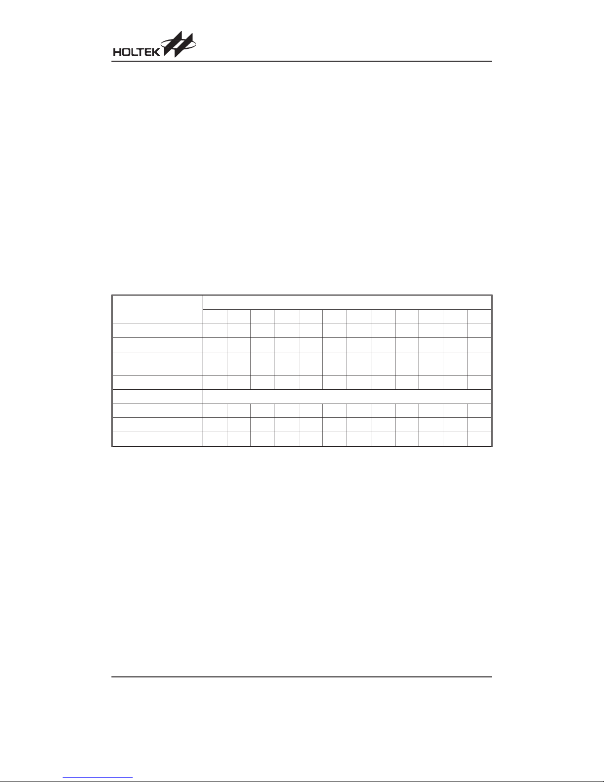
Part No. VDD
Program
Memory
Data
Memory
I/O Timer Int. A/D PWM Stack Package Types
HT46R46
HT46C46
2.2V~
5.5V
1K´14 64´8
13
8-bit´1
3
8-bit´4 8-bit´1
4
16NSOP, 18DIP/SOP,
20SSOP
HT46R47
HT46C47
2.2V~
5.5V
2K´14 64´8
13
8-bit´1
3
9-bit´4 8-bit´1
6
16NSOP, 18DIP/SOP,
20SSOP
HT46R48A
HT46C48A
2.2V~
5.5V
2K´14 88´8
19
8-bit´1
3
9-bit´4 8-bit´1
6
20DIP/SOP,
24SKDIP/SOP/SSOP
HT46R49
2.2V~
5.5V
4K´15 128´8
23
8-bit´1
3
9-bit´4 8-bit´2
6
20DIP/SOP,
24/28SKDIP/SOP
Note:
Part numbers including ²C² are mask version devices, ²R² are OTP devices.
For devices that exist in two package formats, the table reflects the situation for the larger package.
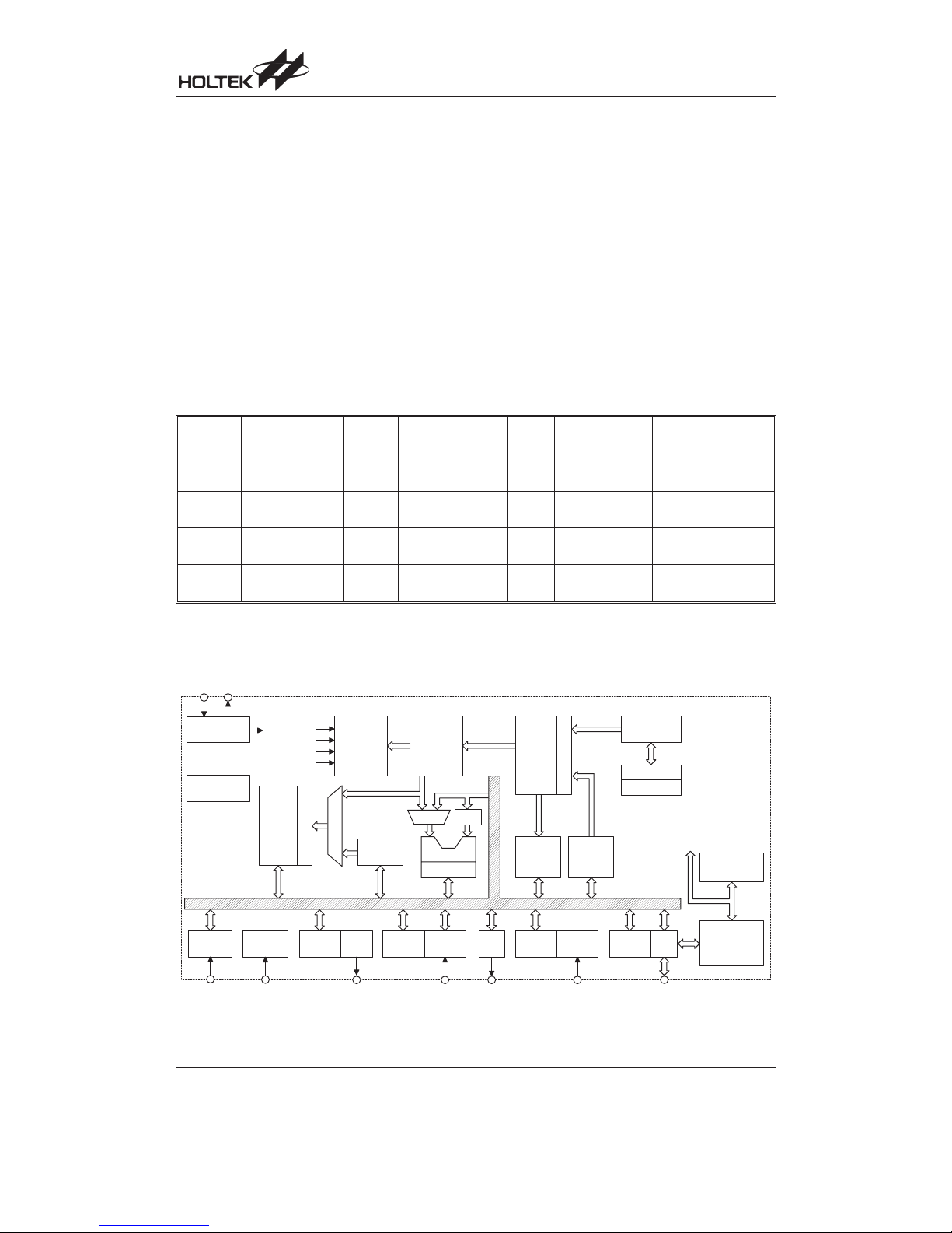
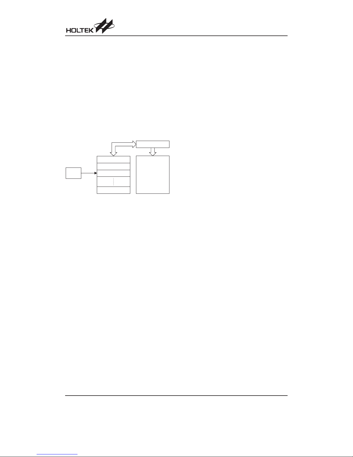
Block Diagram
Note: This block diagram represents the OTP devices, for the mask devices there is no Device Programming
Circuitry.
HT46R46/C46/R47/C47/R48A/C48A/R49
Rev. 1.41 2 December 30, 2008
T i m i n g
G e n e r a t o r
S y s t e m R C /
X ' t a l O s c i l l a t o r
I n s t r u c t i o n
D e c o d e r
I n s t r u c t i o n
R e g i s t e r
W D T
O s c i ll a t o r
D a t a
M e m o r y
A d d r e s s D e c o d e r
M e m o r y
P o i n t e r
M U X
A C C
L o o k - u p
T a b l e
R e g i s t e r
R e s e t &
L V R
C o n f i g .
R e g i s t e r
T i m e r /
C o u n t e r
C o n f i g .
R e g i s t e r
I n t e r r u p t
C i r c u i t
C o n f i g .
R e g i s t e r
I / O
P o r t s
D e v i c e
P r o g r a m m i n g
C i r c u i t r y
C o n f i g u r a t i o n
O p t i o n
P r o g r a m
M e m o r y
A d d r e s s D e c o d e r
S t a c k
S t a c k P o i n t e r
P r o g r a m
C o u n t e r
L o o k - u p
T a b l e
P o i n t e r
T o P r o g r a m
M e m o r y
A L U
S h i f t e r
M
U
X
C o n f i g .
R e g i s t e r
P W M
P F D
A / D
C o n v e r t e r
Device Types
Devices which have the letter ²R² within their part number, indicate that they are OTP devices offering the advantages
of easy and effective program updates, using the Holtek range of development and programming tools. These devices
provide the designer with the means for fast and low-cost product development cycles. Devices which have the letter
²C² within their part number indicate that they are mask version devices. These devices offer a complementary device
for applications that are at a mature state in their design process and have high volume and low cost demands.
Fully pin and functionally compatible with their OTP sister devices, the mask version devices provide the ideal substi
-
tute for products which have gone beyond their development cycle and are facing cost-down demands.
In this datasheet, for convenience, when describing device functions, only the OTP types are mentioned by name,
however the same described functions also apply to the Mask type devices.
Selection Table
Most features are common to all devices, the main feature distinguishing them are Program Memory capacity, I/O
count, A/Dresolution, stack capacityand package types.The following table summarises the main features of each de
-
vice.
Page 3
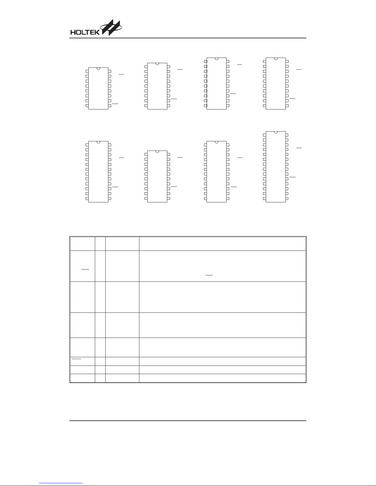
Pin Assignment
Pin Description
HT46R46, HT46R47
Pin Name I/O
Configuration
Option
Description
PA0~PA2
PA3/PFD
PA4/TMR
PA5/INT
PA6~PA7
I/O
Pull-high
Wake-up
PA3 or
PFD
Bidirectional 8-bit input/output port. Each individual pin on this port can be configured as a wake-up input by a configuration option. Software instructions determine
if the pin is a CMOS output or Schmitt Trigger input. Configuration options determine which pins on the port have pull-high resistors. Pins PA3, PA4 and PA5 are
pin-shared with PFD, TMR and INT
, respectively.
PB0/AN0
PB1/AN1
PB2/AN2
PB3/AN3
I/O Pull-high
Bidirectional 4-bit input/output port. Software instructions determine if the pin is a
CMOS output or Schmitt Trigger input. Configuration options determine which pins
on the port have pull-high resistors. PB is pin-shared with the A/D input pins. The
A/D inputs are selected via software instructions. Once selected as an A/D input,
the I/O function and pull-high resistor options are disabled automatically.
PD0/PWM I/O
Pull-high
PD0 or
PWM
Bidirectional 1-bit input/output port. Software instructions determine if the pin is a
CMOS output or Schmitt Trigger input.
A configuration option determines if this pin has a pull-high resistor. The PWM out
-
put is pin-shared with pin PD0 selected via a configuration option.
OSC1
OSC2
I
O
Crystal
or RC
OSC1, OSC2 are connected to an external RC network or external crystal, deter
-
mined by configuration option, for the internalsystem clock. If the RC system clock op
-
tion is selected, pin OSC2 can beused to measure the system clock at 1/4frequency.
RES I
¾
Schmitt Trigger reset input. Active low.
VDD
¾¾
Positive power supply
VSS
¾¾
Negative power supply, ground
Note: 1. Each pin on PA can be programmed through a configuration option to have a wake-up function.
2. Individual pins can be selected to have a pull-high resistor.
3. Pins PB2/AN2~PB3/AN3 exist but are not bonded out on the 16-pin package.
4. unbonded pins should be setup as outputs or as inputs with pull-high resistors to conserve power.
HT46R46/C46/R47/C47/R48A/C48A/R49
Rev. 1.41 3 December 30, 2008
H T 4 6 R 4 6 / H T 4 6 C 4 6
H T 4 6 R 4 7 / H T 4 6 C 4 7
2 0 S S O P - A
P A 4 / T M R
P A 5 / I N T
P A 6
P A 7
O S C 2
O S C 1
V D D
R E S
P D 0 / P W M
N C
2 0
1 9
1 8
1 7
1 6
1 5
1 4
1 3
1 2
1 1
1
2
3
4
5
6
7
8
9
1 0
P A 3 / P F D
P A 2
P A 1
P A 0
P B 3 / A N 3
N C
P B 2 / A N 2
P B 1 / A N 1
P B 0 / A N 0
V S S
H T 4 6 R 4 6 / H T 4 6 C 4 6
H T 4 6 R 4 7 / H T 4 6 C 4 7
1 8 D I P - A / S O P - A
P A 4 / T M R
P A 5 / I N T
P A 6
P A 7
O S C 2
O S C 1
V D D
R E S
P D 0 / P W M
P A 3 / P F D
P A 2
P A 1
P A 0
P B 3 / A N 3
P B 2 / A N 2
P B 1 / A N 1
P B 0 / A N 0
V S S
1 8
1 7
1 6
1 5
1 4
1 3
1 2
1 1
1 0
1
2
3
4
5
6
7
8
9
H T 4 6 R 4 8 A / H T 4 6 C 4 8 A
2 0 D I P - A / S O P - A
P B 5
P A 4 / T M R
P A 5 / I N T
P A 6
P A 7
O S C 2
O S C 1
V D D
R E S
P D 0 / P W M
2 0
1 9
1 8
1 7
1 6
1 5
1 4
1 3
1 2
1 1
1
2
3
4
5
6
7
8
9
1 0
P B 4
P A 3 / P F D
P A 2
P A 1
P A 0
P B 3 / A N 3
P B 2 / A N 2
P B 1 / A N 1
P B 0 / A N 0
V S S
H T 4 6 R 4 8 A / H T 4 6 C 4 8 A
2 4 S K D I P - A / S O P - A / S S O P - A
P B 5
P B 4
P A 3 / P F D
P A 2
P A 1
P A 0
P B 3 / A N 3
P B 2 / A N 2
P B 1 / A N 1
P B 0 / A N 0
V S S
P C 0
P B 6
P B
7
P A 4 / T M R
P A 5 / I N T
P A 6
P A 7
O S C 2
O S C 1
V D D
R E S
P D 0 / P W M
P C 1
2 4
2 3
2 2
2 1
2 0
1 9
1 8
1 7
1 6
1 5
1 4
1 3
1
2
3
4
5
6
7
8
9
1 0
1 1
1 2
H T 4 6 R 4 9
2 8 S K D I P - A / S O P - A
P B 6
P B 7
P A 4 / T M R
P A 5 / I N T
P A 6
P A 7
O S C 2
O S C 1
V D D
R E S
P D 1 / P W M 1
P D 0 / P W M 0
P C 4
P C 3
2 8
2 7
2 6
2 5
2 4
2 3
2 2
2 1
2 0
1 9
1 8
1 7
1 6
1 5
1
2
3
4
5
6
7
8
9
1 0
1 1
1 2
1 3
1 4
P B 5
P B 4
P A 3 / P F D
P A 2
P A 1
P A 0
P B 3 / A N 3
P B 2 / A N 2
P B 1 / A N 1
P B 0 / A N 0
V S S
P C 0
P C 1
P
C 2
P B 5
P B 4
P A 3 / P F D
P A 2
P A 1
P A 0
P B 3 / A N 3
P B 2 / A N 2
P B 1 / A N 1
P B 0 / A N 0
V S S
P C 0
P B 6
P B 7
P A 4 / T M R
P A 5 / I N T
P A 6
P A 7
O S C 2
O S C 1
V D D
R E S
P D 1 / P
W M 1
P D 0 / P W M 0
2 4
2 3
2 2
2 1
2 0
1 9
1 8
1 7
1 6
1 5
1 4
1 3
1
2
3
4
5
6
7
8
9
1 0
1 1
1 2
H T 4 6 R 4 9
2 4 S K D I P - B / S O P - B
H T 4 6 R 4 6 / H T 4 6 C 4 6
H T 4 6 R 4 7 / H T 4 6 C 4 7
1 6 N S O P - A
P A 4 / T M R
P A 5 / I N T
P A 6
P A 7
O S C 2
O S C 1
V D D
R E S
P A 3 / P F D
P A 2
P A 1
P A 0
P B 1 / A N 1
P B 0 / A N 0
V S S
1 6
1 5
1 4
1 3
1 2
1 1
1 0
9
1
2
3
4
5
6
7
8
P D 0 / P W M
H T 4 6 R 4 9
2 0 D I P - A / S O P - A
P A 4 / T M R
P A 5 / I N T
P A 6
P A 7
O S C 2
O S C 1
V D D
R E S
P D 1 / P W M 1
P D 0 / P W M 0
2 0
1 9
1 8
1 7
1 6
1 5
1 4
1 3
1 2
1 1
1
2
3
4
5
6
7
8
9
1 0
P A 3 / P F D
P A 2
P A 1
P A 0
P B 3 / A N 3
P B 2 / A N 2
P B 1 / A N 1
P B 0 / A N 0
V S S
P C 0
Page 4

HT46R48A
Pin Name I/O
Configuration
Option
Description
PA0~PA2
PA3/PFD
PA4/TMR
PA5/INT
PA6~PA7
I/O
Pull-high
Wake-up
PA3 or PFD
Bidirectional 8-bit input/output port. Each individual pin on this port can be config
ured as a wake-up input by a configuration option. Software instructions determine
if the pin is a CMOS output or Schmitt Trigger input. Configuration options deter
mine which pins on the port have pull-high resistors. Pins PA3, PA4 and PA5 are
pin-shared with PFD, TMR and INT
, respectively.
PB0/AN0
PB1/AN1
PB2/AN2
PB3/AN3
PB4~PB7
I/O Pull-high
Bidirectional 8-bit input/output port. Software instructions determine if the pin is a
CMOS output or Schmitt Trigger input. Configuration options determine which pins
on the port have pull-high resistors. PB is pin-shared with the A/D input pins. The
A/D inputs are selected via software instructions. Once selected as an A/D input,
the I/O function and pull-high resistor options are disabled automatically.
PC0~PC1 I/O Pull-high
Bidirectional 2-bit input/output port. Software instructions determine if the pin is a
CMOS output or Schmitt Trigger input. Configuration options determine which pins
on the port have pull-high resistors.
PD0/PWM I/O
Pull-high
I/O or PWM
Bidirectional 1-bit input/output port. Software instructions determine if the pin is a
CMOS output or Schmitt Trigger input. Configuration option determines if this pin
has a pull-high resistor. The PWM output is pin-shared with pin PD0 selected via a
configuration option.
OSC1
OSC2
I
O
Crystal or RC
OSC1, OSC2 are connected to an external RC network or external crystal, deter
mined by configuration option, for the internal system clock. If the RC system clock
option is selected, pin OSC2 can be used to measure the system clock at 1/4 fre
quency.
RES I
¾
Schmitt Trigger reset input. Active low.
VDD
¾¾
Positive power supply
VSS
¾¾
Negative power supply, ground
Note: 1. Each pin on PA can be programmed through a configuration option to have a wake-up function.
2. Individual pins can be selected to have a pull-high resistor.
3. Pins PB4~PB7 exist but are not bonded out on the 20-pin package.
4. Unbonded pins should be setup as outputs or as inputs with pull-high resistors to conserve power.
HT46R46/C46/R47/C47/R48A/C48A/R49
Rev. 1.41 4 December 30, 2008
Page 5

HT46R49
Pin Name I/O
Configuration
Option
Description
PA0~PA2
PA3/PFD
PA4/TMR
PA5/INT
PA6~PA7
I/O
Pull-high
Wake-up
PA3 or PFD
Bidirectional 8-bit input/output port. Each individual pin on this port can be config
-
ured as a wake-up input by a configuration option. Software instructions deter
-
mine if the pin is a CMOS output or Schmitt Trigger input. Configuration options
determine which pins on the port have pull-high resistors. Pins PA3, PA4 and PA5
are pin-shared with PFD, TMR and INT
, respectively.
PB0/AN0
PB1/AN1
PB2/AN2
PB3/AN3
PB4~PB7
I/O Pull-high
Bidirectional 8-bit input/output port. Software instructions determine if the pin is a
CMOS output or Schmitt Trigger input. Configuration options determine which
pins on the port have pull-high resistors. PB is pin-shared with the A/D input pins.
The A/D inputs are selected via software instructions. Once selected as an A/D in
-
put, the I/O function and pull-high resistor options are disabled automatically.
PC0~PC4 I/O Pull-high
Bidirectional 5-bit input/output port. Software instructions determine if the pin is a
CMOS output or Schmitt Trigger input. Configuration options determine which
pins on the port have pull-high resistors.
PD0/PWM0
PD1/PWM1
I/O
Pull-high
I/O or PWM
Bidirectional 2-bit input/output port. Software instructions determine if the pin is a
CMOS output or Schmitt Trigger input. Configuration option determines if this pin
has a pull-high resistor. The PWM output are pin-shared with pins PD0 and PD1
selected via a configuration option.
OSC1
OSC2
I
O
Crystal or RC
OSC1, OSC2 are connected to an external RC network or external crystal, deter
-
mined by configuration option, for the internal system clock. If the RC system
clock option is selected, pin OSC2 can be used to measure the system clock at
1/4 frequency.
RES I
¾
Schmitt Trigger reset input. Active low.
VDD
¾¾
Positive power supply
VSS
¾¾
Negative power supply, ground
Note: 1. Each pin on PA can be programmed through a configuration option to have a wake-up function.
2. Individual pins can be selected to have a pull-high resistor.
3. Pins PC1~PC4 exist but are not bonded out on the 20-pin and 24-pin package.
Pins PB4~PB7 exist but are not bonded out on the 20-pin package.
4. Unbonded pins should be setup as outputs or as inputs with pull-high resistors to conserve power.
Absolute Maximum Ratings
Supply Voltage...........................VSS-0.3V to VSS+6.0V
Storage Temperature ............................-50°Cto125°C
Input Voltage..............................V
SS
-0.3V to VDD+0.3V
Operating Temperature...........................-40°Cto85°C
I
OL
Total ..............................................................150mA
I
OH
Total............................................................-100mA
Total Power Dissipation .....................................500mW
Note: These are stress ratings only. Stresses exceeding the range specified under ²Absolute Maximum Ratings² may
cause substantial damage to the device. Functional operation of this device at other conditions beyond those listed
in the specification is not implied and prolonged exposure to extreme conditions may affect device reliability.
HT46R46/C46/R47/C47/R48A/C48A/R49
Rev. 1.41 5 December 30, 2008
Page 6
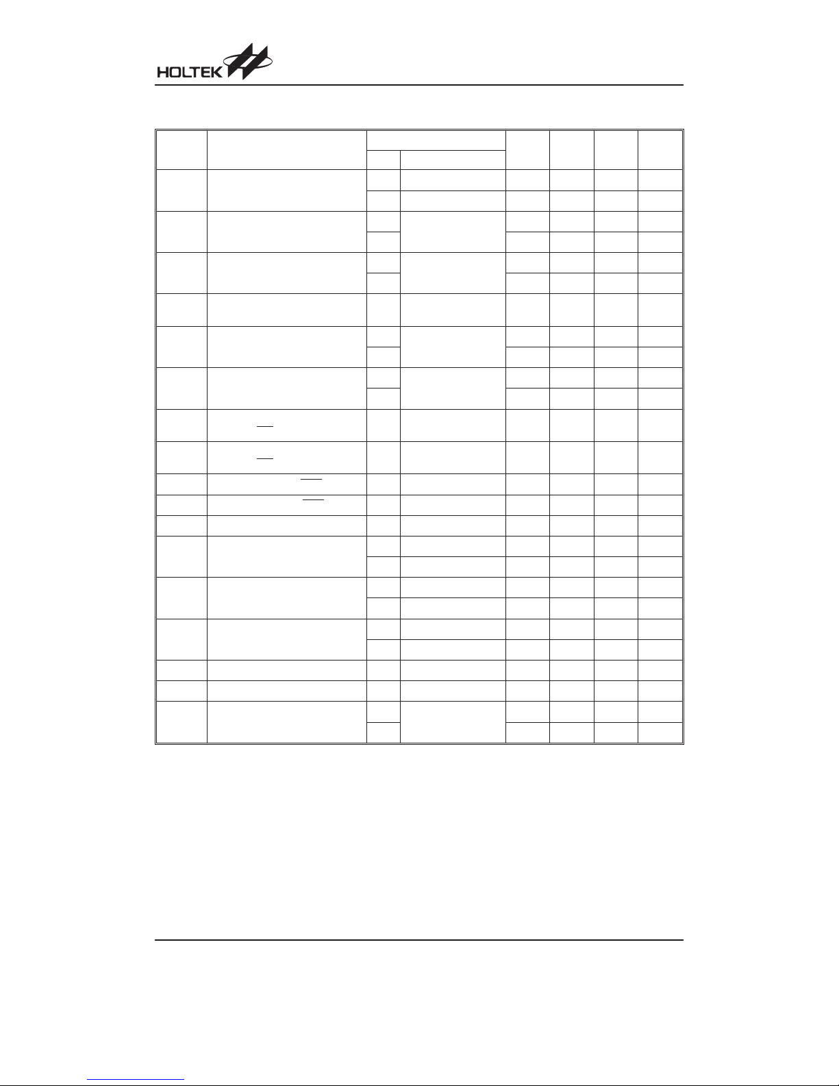
D.C. Characteristics
Ta=25°C
Symbol Parameter
Test Conditions
Min. Typ. Max. Unit
V
DD
Conditions
V
DD
Operating Voltage
¾
f
SYS
=4MHz
2.2
¾
5.5 V
¾
f
SYS
=8MHz
3.3
¾
5.5 V
I
DD1
Operating Current
(Crystal OSC)
3V
No load, f
SYS
=4MHz
ADC disable
¾
0.6 1.5 mA
5V
¾
24mA
I
DD2
Operating Current
(RC OSC)
3V
No load, f
SYS
=4MHz
ADC disable
¾
0.8 1.5 mA
5V
¾
2.5 4 mA
I
DD3
Operating Current
(Crystal OSC, RC OSC)
5V
No load, f
SYS
=8MHz
ADC disable
¾
48mA
I
STB1
Standby Current
(WDT Enabled)
3V
No load,
system HALT
¾¾
5
mA
5V
¾¾
10
mA
I
STB2
Standby Current
(WDT Disabled)
3V
No load,
system HALT
¾¾
1
mA
5V
¾¾
2
mA
V
IL1
Input Low Voltage for I/O Ports,
TMR and INT
¾¾
0
¾
0.3V
DD
V
V
IH1
Input High Voltage for I/O Ports,
TMR and INT
¾¾
0.7V
DD
¾
V
DD
V
V
IL2
Input Low Voltage (RES)
¾¾
0
¾
0.4V
DD
V
V
IH2
Input High Voltage (RES)
¾¾
0.9V
DD
¾
V
DD
V
V
LVR
Low Voltage Reset
¾¾
2.7 3.0 3.3 V
I
OL
I/O Port Sink Current
3V
V
OL
=0.1V
DD
48
¾
mA
5V
V
OL
=0.1V
DD
10 20
¾
mA
I
OH
I/O Port Source Current
3V
V
OH
=0.9V
DD
-2 -4 ¾
mA
5V
V
OH
=0.9V
DD
-5 -10 ¾
mA
R
PH
Pull-high Resistance
3V
¾
20 60 100
kW
5V
¾
10 30 50
kW
V
AD
A/D Input Voltage
¾¾
0
¾
V
DD
V
E
AD
A/D Conversion Error
¾¾ ¾±0.5 ±1
LSB
I
ADC
Additional Power Consumption
if A/D Converter is Used
3V
¾
¾
0.5 1 mA
5V
¾
1.5 3 mA
HT46R46/C46/R47/C47/R48A/C48A/R49
Rev. 1.41 6 December 30, 2008
Page 7
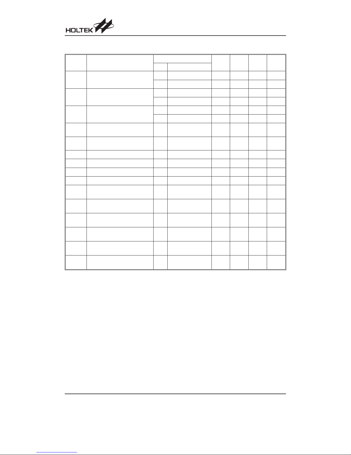
A.C. Characteristics
Ta=25°C
Symbol Parameter
Test Conditions
Min. Typ. Max. Unit
V
DD
Conditions
f
SYS
System Clock
¾
2.2V~5.5V 400
¾
4000 kHz
¾
3.3V~5.5V 400
¾
8000 kHz
f
TIMER
Timer I/P Frequency
(TMR)
¾
2.2V~5.5V 0
¾
4000 kHz
¾
3.3V~5.5V 0
¾
8000 kHz
t
WDTOSC
Watchdog Oscillator Period
3V
¾
45 90 180
ms
5V
¾
32 65 130
ms
t
WDT1
Watchdog Time-out Period
(RC)
¾¾
2
15
¾
2
16
t
WDTOSC
t
WDT2
Watchdog Time-out Period
(System Clock)
¾¾
2
17
¾
2
18
t
SYS
t
RES
External Reset Low Pulse Width
¾¾
1
¾¾ms
t
SST
System Start-up Timer Period
¾
Wake-up from HALT
¾
1024
¾
*t
SYS
t
LVR
Low Voltage Reset Time
¾¾
0.25 1 2 ms
t
INT
Interrupt Pulse Width
¾¾
1
¾¾ms
t
AD1
A/D Clock Period HT46R46
¾¾
0.5
¾¾ms
t
AD2
A/D Clock Period HT46R47/HT46R48A/HT46R49
¾¾
1
¾¾ms
t
ADC1
A/D Conversion Time HT46R46
¾¾ ¾64¾
t
AD1
t
ADC2
A/D Conversion Time HT46R47/HT46R48A/HT46R49
¾¾ ¾76¾
t
AD2
t
ADCS1
A/D Sampling Time HT46R46
¾¾ ¾32¾
t
AD1
t
ADCS2
A/D Sampling Time HT46R47/HT46R48A/HT46R49
¾¾ ¾32¾
t
AD2
Note: *t
SYS
=1/f
SYS
HT46R46/C46/R47/C47/R48A/C48A/R49
Rev. 1.41 7 December 30, 2008
Page 8

HT46R46/C46/R47/C47/R48A/C48A/R49
Rev. 1.41 8 December 30, 2008
System Architecture
A key factor in the high-performance features of the
Holtek range of Cost-Effective A/D Type
microcontrollers is attributed to the internal system ar
chitecture. The range of devices take advantage of the
usual features found within RISC microcontrollers pro
viding increased speed of operation and enhanced per
formance. The pipelining scheme is implemented in
such a way that instruction fetching and instruction exe
cution are overlapped, hence instructions are effectively
executed in one cycle, with the exception of branch or
call instructions. An 8-bit wide ALU is used in practically
all operations of the instruction set. It carries out arith
metic operations, logic operations, rotation, increment,
decrement, branch decisions, etc. The internal data
path is simplified by moving data through the Accumula
tor and the ALU. Certain internal registers are imple
mented in the Data Memory and can be directly or
indirectly addressed. The simple addressing methods of
these registers along with additional architectural fea
tures ensure that a minimum of external components is
required to provide a functional I/O and A/D control sys
tem with maximum reliability and flexibility. This makes
these devices suitable for low-cost, high-volume pro
duction for controller applications requiring from 1K up
to 4K words of Program Memory and 64 to 128 bytes of
Data Memory storage.
Clocking and Pipelining
The main system clock, derived from either a Crys
-
tal/Resonator or RC oscillator is subdivided into four in
ternally generated non-overlapping clocks, T1~T4. The
Program Counter is incremented at the beginning of the
T1 clock during which time a new instruction is fetched.
The remaining T2~T4 clocks carry out the decoding and
execution functions. In this way, one T1~T4 clock cycle
forms one instruction cycle. Although the fetching and
execution of instructions takes place in consecutive in
struction cycles, the pipelining structure of the
microcontroller ensures that instructions are effectively
executed in one instruction cycle. The exception to this
are instructions where the contents of the Program
Counter are changed, such as subroutine calls or
jumps, in which case the instruction will take one more
instruction cycle to execute.
When the RC oscillator is used, OSC2 is freed for use as
a T1 phase clock synchronizing pin. This T1 phase clock
has afrequency of f
SYS
/4 witha 1:3 high/low duty cycle.
For instructions involving branches, such as jump or call
instructions, two machine cycles are required to com
plete instruction execution. An extra cycle is required as
the program takes one cycle to first obtain the actual
jump or call address and then another cycle to actually
execute the branch. The requirement for this extra cycle
should be taken into account by programmers in timing
sensitive applications
F e t c h I n s t . ( P C )
E x e c u t e I n s t . ( P C - 1 )
F e t c h I n s t . ( P C + 1 )
E x e c u t e I n s t . ( P C )
F e t c h I n s t . ( P C + 2 )
E x e c u t e I n s t . ( P C + 1 )
P C P C + 1 P C + 2
O s c i l l a t o r C l o c k
( S y s t e m C l o c k )
P h a s e C l o c k T 1
P r o g r a m C o u n t e r
P h a s e C l o c k T 2
P h a s e C l o c k T 3
P h a s e C l o c k T 4
P i p e l i n i n g
System Clocking and Pipelining
F e t c h I n s t . 1 E x e c u t e I n s t . 1
F e t c h I n s t . 2
F l u s h P i p e l i n e
1
2
3
4
5
6
D E L A Y :
M O V A , [ 1 2 H ]
C A L L D E L A Y
C P L [ 1 2 H ]
:
:
N O P
E x e c u t e I n s t . 2
F e t c h I n s t . 3
F e t c h I n s t . 6 E x e c u t e I n s t . 6
F e t c h I n s t . 7
Instruction Fetching
Page 9
HT46R46/C46/R47/C47/R48A/C48A/R49
Rev. 1.41 9 December 30, 2008
Program Counter
During program execution, the Program Counter is used
to keep track of the address of the next instruction to be
executed. It is automatically incremented by one each
time an instruction is executed except for instructions,
such as ²JMP² or ²CALL² that demand a jump to a
non-consecutive Program Memory address. For the
Cost-Effective A/D Type series of microcontrollers, note
that the Program Counter width varies with the Program
Memory capacity depending upon which device is se
lected. However, it must be noted that only the lower 8
bits, known as the Program Counter Low Register, are
directly addressable by user.
When executing instructions requiring jumps to
non-consecutive addresses such as a jump instruction,
a subroutine call, interrupt or reset, etc., the
microcontroller manages program control by loading the
required address into the Program Counter. For condi
tional skip instructions, once the condition has been
met, the next instruction, which has already been
fetched during the present instruction execution, is dis
-
carded and a dummy cycle takes its place while the cor
-
rect instruction is obtained.
The lower byte of the Program Counter, known as the
Program Counter Low register or PCL, is available for
program control and is a readable and writable register.
By transferring data directly into this register, a short
program jump can be executed directly, however, as
only this low byte is available for manipulation, the
jumps are limited to the present page of memory, that is
256 locations. When such program jumps are executed
it should also be noted that a dummy cycle will be in
-
serted.
The lower byte of the Program Counter is fully accessi
ble under program control. Manipulating the PCL might
cause program branching, so an extra cycle is needed
to pre-fetch. Further information on the PCL register can
be found in the Special Function Register section.
Mode
Program Counter Bits
b11 b10 b9 b8 b7 b6 b5 b4 b3 b2 b1 b0
Initial Reset 000000000000
External Interrupt 000000000100
Timer/Event Counter
Overflow
000000001000
A/D Converter Interrupt 000000001100
Skip Program Counter + 2
Loading PCL PC11 PC10 PC9 PC8 @7 @6 @5 @4 @3 @2 @1 @0
Jump, Call Branch #11 #10 #9 #8 #7 #6 #5 #4 #3 #2 #1 #0
Return from Subroutine S11 S10 S9 S8 S7 S6 S5 S4 S3 S2 S1 S0
Program Counter
Note: PC11~PC8: Current Program Counter bits
@7~@0: PCL bits
#11~#0: Instruction code address bits
S11~S0: Stack register bits
For the HT46R49, the Program Counter is 12 bits wide, i.e. from b11~b0.
For the HT46R47 and HT46R48A, the Program Counter is 11 bits wide, i.e. From
b10~b0, therefore the b11 column in the table is not applicable.
For the HT46R46, the Program Counter is 10 bits wide, i.e. from b9~b0, therefore the b11 and
b10 the columns in the table are not applicable.
Page 10
HT46R46/C46/R47/C47/R48A/C48A/R49
Rev. 1.41 10 December 30, 2008
Stack
This is a special part of the memory which is used to
save the contents of the Program Counter only. The
stack can have either 4 or 6 levels depending upon
which device is selected and is neither part of the data
nor part of the program space, and is neither readable
nor writable. The activated level is indexed by the Stack
Pointer, SP, and is neither readable nor writable. At a
subroutine call or interrupt acknowledge signal, the con
tents of the Program Counter are pushed onto the stack.
At the end of a subroutine or an interrupt routine, sig
naled by a return instruction, RET or RETI, the Program
Counter is restored to its previous value from the stack.
After a device reset, the Stack Pointer will point to the
top of the stack.
If the stack is full and an enabled interrupt takes place,
the interrupt request flag will be recorded but the acknowledge signal will be inhibited. When the Stack
Pointer is decremented, by RET or RETI, the interrupt
will be serviced. This feature prevents stack overflow allowing the programmer to use the structure more easily.
However, when the stack is full, a CALL subroutine instruction can still be executed which will result in a stack
overflow. Precautions should be taken to avoid such
cases which might cause unpredictable program
branching.
Note: Forthe HT46R46, 4levels of stackare available
and for the HT46R47,HT46R48A and
HT46R49, 6 levels of stack are available.
Arithmetic and Logic Unit - ALU
The arithmetic-logic unit or ALU is a critical area of the
microcontroller that carries out arithmetic and logic op
erations of the instruction set. Connected to the main
microcontroller data bus, the ALU receives related in
struction codes and performs the required arithmetic or
logical operations after which the result will be placed in
the specified register. As these ALU calculation or oper
ations may result in carry, borrow or other status
changes, the status register will be correspondingly up
dated to reflect these changes. The ALU supports the
following functions:
·
Arithmetic operations: ADD, ADDM, ADC, ADCM,
SUB, SUBM, SBC, SBCM, DAA
·
Logic operations: AND, OR, XOR, ANDM, ORM,
XORM, CPL, CPLA
·
Rotation RRA, RR, RRCA, RRC, RLA, RL, RLCA,
RLC
·
Increment and Decrement INCA, INC, DECA, DEC
·
Branch decision, JMP, SZ, SZA, SNZ, SIZ, SDZ,
SIZA, SDZA, CALL, RET, RETI
Program Memory
The Program Memory is the location wherethe user code
or program is stored. For microcontrollers, two types of
Program Memory are usually supplied. The first type is
the One-Time Programmable, OTP, memory where us
ers can program their application code into the device.
Devices with OTP memory are denoted by having an ²R²
within their device name. By using the appropriate pro
gramming tools, OTP devices offer users the flexibility to
freely develop their applications which may be useful
during debug or for products requiring frequent upgrades
or program changes. OTP devices are also applicable for
use in applications that require low or medium volume
production runs. The other type of memory is the mask
ROM memory, denoted by having a ²C² within the device
name. These devices offer the most cost effective solu
tions for high volume products.
Structure
The Program Memory has a capacity of 1K by 14, 2K by
14 or 4K by 15 bits depending upon which device is selected. The Program Memory is addressed by the Program Counter and also contains data, table information
and interrupt entries. Table data, which can be setup in
any location within the Program Memory, is addressed
by separate table pointer registers.
Special Vectors
Within the Program Memory, certain locations are re
served for special usage such as reset and interrupts.
·
Location 000H
This vector is reserved for use by the device reset for
program initialisation. After a device reset is initiated, the
program will jump to this location and begin execution.
·
Location 004H
This vector is used by the external interrupt. If the ex
-
ternal interrupt pin on the device goes low, the pro
-
gram will jump to this location and begin execution if
the external interrupt is enabled and the stack is not
full.
·
Location 008H
This internal vector is used by the Timer/Event Coun
-
ter. If a counter overflow occurs, the program will jump
to this location and begin execution if the timer/event
counter interrupt is enabled and the stack is not full.
·
Location 00CH
This internal vector is used by the A/D converter.
When an A/D conversion cycle is complete, the pro
-
gram will jump to this location and begin execution if
the A/D interrupt is enabled and the stack is not full.
P r o g r a m C o u n t e r
S t a c k L e v e l 1
S t a c k L e v e l 2
S t a c k L e v e l 3
S t a c k L e v e l N
P r o g r a m
M e m o r y
T o p o f S t a c k
S t a c k
P o i n t e r
B o t t o m o f S t a c k
Page 11
HT46R46/C46/R47/C47/R48A/C48A/R49
Rev. 1.41 11 December 30, 2008
Look-up Table
Any location within the Program Memory can be defined
as a look-up table where programmers can store fixed
data. To use the look-up table, the table pointer must
first be setup by placing the lower order address of the
look up data to be retrieved in the table pointer register,
TBLP. This register defines the lower 8-bit address of
the look-up table.
After setting up the table pointer, the table data can be
retrieved from the current Program Memory page or last
Program Memory page using the ²TABRDC[m]² or
²TABRDL[m]² instructions, respectively. When these in
structions are executed, the lower order table byte from
the Program Memory will be transferred to the user de
fined Data Memory register [m] as specified in the in
struction. The higher order table data byte from the
Program Memory will be transferred to the TBLH special
register. Any unused bits in this transferred higher order
byte will be read as ²0².
The following diagram illustrates the addressing/data
flow of the look-up table:
Table Program Example
The following example shows how the table pointer and
table data is defined and retrieved from the HT46R47
microcontroller. This example uses raw table data located in the last page which is stored there using the
ORG statement. The value at this ORG statement is
²700H² which refers to the start address of the last page
within the 2K Program Memory of the HT46R47
microcontroller. The table pointer is setup here to have
an initial value of ²06H². This will ensure that the first
data read from the data table will be at the Program
Memory address ²706H² or 6 locations after the start of
the last page. Note that the value for the table pointer is
referenced to the first address of the present page if the
²TABRDC [m]² instruction is being used. The high byte
of the table data which in this case is equal to zero will
be transferred to the TBLH register automatically when
the ²TABRDL [m]² instruction is executed.
3 F F H
N o t I m p l e m e n t e d
1 5 b i t s
1 4 b i t s1 4 b i t s
8 0 0 H
F F F H
0 1 4 H
I n i t i a l i s a t i o n
V e c t o r
E x t e r n a l
I n t e r r u p t V e c t o r
I n i t i a l i s a t i o n
V e c t o r
E x t e r n a l
I n t e r r u p t V e c t o r
T i m e r / E v e n t C o u n t e r
I n t e r r u p t V e c t o r
I n i t i a l i s a t i o n
V e c t o r
E x t e r n a l
I n t e r r u p t V e c t o r
T i m e r / E v e n t C o u n t e r
I n t e r r u p t V e c t o r
H T 4 6 R 4 7
H T 4 6 R 4 8 A H T 4 6 R 4 9H T 4 6 R 4 6
A / D C o n v e r t e r
I n t e r r u p t V e c t o r
A / D C o n v e r t e r
I n t e r r u p t V e c t o r
A / D C o n v e r t e r
I n t e r r u p t V e c t o r
T i m e r / E v e n t C o u n t e r
I n t e r r u p t V e c t o r
0 0 0 H
0 0 4 H
0 0 8 H
0 0 C H
0 1 0 H
3 0 0 H
7 F F H
4 0 0 H
Program Memory Structure
P r o g r a m
M e m o r y
P r o g r a m C o u n t e r
H i g h B y t e
T B L P
T B L H S p e c i f i e d b y [ m ]
T a b l e C o n t e n t s H i g h B y t e
T a b l e C o n t e n t s L o w B y
t e
Page 12

HT46R46/C46/R47/C47/R48A/C48A/R49
Rev. 1.41 12 December 30, 2008
tempreg1 db ? ; temporary register #1
tempreg2 db ? ; temporary register #2
:
:
mov a,06h ; initialise table pointer - note that this address
; is referenced
mov tblp,a ; to the last page or present page
:
:
tabrdl tempreg1 ; transfers value in table referenced by table pointer
; to tempregl
; data at prog. memory address ²706H² transferred to
; tempreg1 and TBLH
dec tblp ; reduce value of table pointer by one
tabrdl tempreg2 ; transfers value in table referenced by table pointer
; to tempreg2
; data at prog.memory address ²705H² transferred to
; tempreg2 and TBLH
; in this example the data ²1AH² is transferred to
; tempreg1 and data ²0FH² to register tempreg2
; the value ²00H² will be transferred to the high byte
; register TBLH
:
:
org 700h ; sets initial address of last page (for HT46R47)
Dc 00Ah, 00Bh, 00Ch, 00Dh, 00Eh, 00Fh, 01Ah, 01Bh
:
:
Because the TBLH register is a read-only register and
cannot be restored, care should be taken to ensure its
protection if both the main routine and Interrupt Service
Routine use table read instructions. If using the table
read instructions, the Interrupt Service Routines may
change the value of the TBLH and subsequently cause
errors if used again by the main routine. As a rule it is
recommended that simultaneous use of the table read
instructions should be avoided. However, in situations
where simultaneous use cannot be avoided, the interrupts should be disabled prior to the execution of any
main routine table-read instructions. Note that all table
related instructions require two instruction cycles to
complete their operation.
Data Memory
The Data Memory is a volatile area of 8-bit wide RAM
internal memory and is the location where temporary information is stored. Divided into two sections, the first of
these is an area of RAM where special function registers
are located. These registers have fixed locations and
are necessary for correct operation of the device. Many
of these registers can be read from and written to directly under program control, however, some remain
protected from user manipulation. The second area of
Data Memory is reserved for general purpose use. All
locations within this area are read and write accessible
under program control.
Instruction
Table Location Bits
b11 b10 b9 b8 b7 b6 b5 b4 b3 b2 b1 b0
TABRDC
[m] PC11 PC10 PC9 PC8 @7 @6 @5 @4 @3 @2 @1 @0
TABRDL
[m]1111@7@6@5@4@3@2@1@0
Table Location
Note: PC11~PC8: Current Program Counter bits
@7~@0: Table Pointer TBLP bits
For the HT46R49 the Table address location is 12 bits, i.e. from b11~b0.
For the HT46R47 and HT46R48A, the Table address location is 11 bits, i.e. from b10~b0.
For the HT46R46, the Table address location is 10 bits, i.e. from b9~b0.
Page 13

HT46R46/C46/R47/C47/R48A/C48A/R49
Rev. 1.41 13 December 30, 2008
Structure
The two sections of Data Memory, the Special Purpose
and General Purpose Data Memory are located at con
secutive locations. All are implemented in RAM and are
8 bits wide but the length of each memory section is dic
tated by the type of microcontroller chosen. The start
address of the Data Memory for all devices is the ad
-
dress ²00H². Registers which are common to all
microcontrollers, such as ACC, PCL, etc., have the
same Data Memory address.
General Purpose Data Memory
All microcontroller programs require an area of
read/write memory where temporary data can be stored
and retrieved for use later. It is this area of RAM memory
that is known as General Purpose Data Memory. This
area of Data Memory is fully accessible by the user pro
gram for both read and write operations. By using the
²SET [m].i² and ²CLR [m].i² instructions individual bits
can be set or reset under program control giving the
user a large range of flexibility for bit manipulation in the
Data Memory.
Special Purpose Data Memory
This area of Data Memory is where registers, necessary
for the correct operation of the microcontroller, are
stored. Most of the registers are both readable and
writable but some are protected and are readable only,
the details of which are located under the relevant Spe
cial Function Register section. Note that for locations
that areunused, any readinstruction to these addresses
will return the value ²00H².
Special Function Registers
To ensure successful operation of the microcontroller,
certain internal registers are implemented in the Data
Memory area. These registers ensure correct operation
of internal functions such as timers, interrupts, etc., as
well as external functions such as I/O data control and
A/D converter operation. The location of these registers
within the Data Memory begins at the address 00H. Any
unused Data Memory locations between these special
function registers and the point where the General Pur
pose Memory begins is reserved for future expansion
purposes, attempting to read data from these locations
will return a value of 00H.
Indirect Addressing Register - IAR
The IAR register, located at Data Memory address
²00H², is not physically implemented. This special register allows what is known as indirect addressing, which
permits data manipulation using Memory Pointers instead of the usual direct memory addressing method
where the actual memory address is defined. Any ac
tions on the IAR register will result in corresponding
read/write operations to the memory location specified
by the Memory Pointer MP. Reading the IAR register in
-
directly will return a result of ²00H² and writing to the
register indirectly will result in no operation.
Memory Pointer - MP
One Memory Pointer, known as MP, is physically imple
mented in Data Memory. The Memory Pointer can be
written to and manipulated in the same way as normal
registers providing an easy way of addressing and
tracking data. When using any operation on the indirect
addressing register IAR, it is actually the address speci
fied by the Memory Pointer that the microcontroller will
be directed to.
For devices with 64 or 88 bytes of RAM Data Memory,
bit 7 of the Memory Pointer is not implemented. How
ever, it must be noted that when the Memory Pointer for
these devices is read, bit 7 will be read as high.
G e n e r a l P u r p o s e
D a t a M e m o r y
S p e c i a l P u r p o s e
D a t a M e m o r y
0 0 H
4 0 H
B F H
3 F H
G e n e r a l P u r p o s e
D a t a M e m o r y
S p e c i a l P u r p o s e
D a t a M e m o r y
0 0 H
4 0 H
7 F H
3 F H
H T 4 6 R 4 6 a n d H T 4 6 R 4 7
H T 4 6 R 4 9
G e n e r a l P u r p o s e
D a t a M e m o r y
S p e c i a l P u r p o s e
D a t a M e m o r y
0 0 H
2 8 H
7 F H
2 7 H
H T 4 6 R 4 8 A
Data Memory Structure
Note:
Most ofthe Data Memorybits can be directly manipulated using the ²SET [m].i² and ²CLR [m].i² with the excep
-
tion ofa few dedicated bits. The Data Memory can also be accessed through thememory pointer register MP.
Page 14
HT46R46/C46/R47/C47/R48A/C48A/R49
Rev. 1.41 14 December 30, 2008
The following example shows how to clear a section of four RAM locations already defined as locations adres1 to
adres4.
data .section ¢data¢
adres1 db ?
adres2 db ?
adres3 db ?
adres4 db ?
block db ?
code .section at 0 ¢code¢
org 00h
start:
mov a,04h ; setup size of block
mov block,a
mov a,offset adres1 ; Accumulator loaded with first RAM address
mov mp,a ; setup memory pointer with first RAM address
loop:
clr IAR ; clear the data at address defined by MP
inc mp ; increment memory pointer
sdz block ; check if last memory location has been cleared
jmp loop
continue:
The importantpoint to note here is that in the example shownabove, no reference is made to specific RAM addresses.
0 0 H
0 1 H
0 2 H
0 3 H
0 4 H
0 5 H
0 6 H
0 7 H
0 8 H
0 9 H
0 A H
0 B H
0 C H
0 D H
0 E H
0 F H
1 0 H
1 1 H
1 2 H
1 3 H
1 4 H
1 5 H
1 6 H
1 7 H
1 8 H
1 9 H
1 A H
1 B H
1 C H
1 D H
1 E H
1 F H
2 0 H
2 1
H
2 2 H
2 3 H : U n u s e d , r e a d a s " 0 0 "
I A R
M P
A C C
P C L
T B L P
T B L H
S T A T U S
I N T C
T M R
T M R C
P A
P A C
P B
P B C
P D
P D C
P W M
A D R
A D C R
A C S R
H T 4 6 R 4 6
I A R
M P
A C C
P C L
T B L P
T B L H
S T A T U S
I N T C
T M R
T M R C
P A
P A C
P B
P B C
P D
P D C
P W M
A D R L
A D R H
A D C R
A C S R
H T 4 6 R 4 7
I A R
M P
A C C
P C L
T B L P
T B L H
S T A T U S
I N T C
T M R
T M R C
P A
P A C
P B
P B C
P C
P C C
P D
P D C
P W M
A D R L
A D R H
A D C R
A C S R
H T 4 6 R 4 8 A
I A R
M P
A C C
P C L
T B L P
T B L H
S T A T U S
I N T C
T M R
T M R C
P A
P A C
P B
P B C
P C
P C C
P D
P D C
P W M 0
P W M 1
A D R L
A D R H
A D C R
A C S R
H T 4 6 R 4 9
Special Purpose Data Memory
Page 15
HT46R46/C46/R47/C47/R48A/C48A/R49
Rev. 1.41 15 December 30, 2008
Accumulator - ACC
The Accumulator is central to the operation of any
microcontroller and is closely related with operations
carried out by the ALU. The Accumulator is the place
where all intermediate results from the ALU are stored.
Without the Accumulator it would be necessary to write
the result of each calculation or logical operation such
as addition, subtraction, shift, etc., to the Data Memory
resulting in higher programming and timing overheads.
Data transfer operations usually involve the temporary
storage function of the Accumulator; for example, when
transferring data between one user defined register and
another, it is necessary to do this by passing the data
through the Accumulator as no direct transfer between
two registers is permitted.
Program Counter Low Register - PCL
To provide additional program control functions, the low
byte of the Program Counter is made accessible to pro
grammers by locating it within the Special Purpose area
of the Data Memory. By manipulating this register, direct
jumps to other program locations are easily imple
mented. Loading a value directly into this PCL register
will cause a jump to the specified Program Memory lo
cation, however, as the register is only 8-bit wide, only
jumps within the current Program Memory page are permitted. When such operations are used, note that a
dummy cycle will be inserted.
Look-up Table Registers - TBLP, TBLH
These two special function registers are used to control
operation of the look-up table which is stored in the Program Memory. TBLP is the table pointer and indicates
the location where the table data is located. Its value
must be setup before any table read commands are ex
ecuted. Its value can be changed, for example using the
²INC² or ²DEC² instructions, allowing for easy table data
pointing and reading. TBLH is the location where the
high order byte of the table data is stored after a table
read data instruction has been executed. Note that the
lower order table data byte is transferred to a user de
fined location.
Status Register - STATUS
This 8-bit register contains the zero flag (Z), carry flag
(C), auxiliary carry flag (AC), overflow flag (OV), power
down flag (PDF), and watchdog time-out flag (TO).
These arithmetic/logical operation and system manage
ment flagsare used to record the status and operation of
the microcontroller.
With the exception of the TO and PDF flags, bits in the
status register can be altered by instructions like most
other registers. Any data written into the status register
will not change the TO or PDF flag. In addition, opera
tions related to the status register may give different re
sults due to the different instruction operations. The TO
flag can be affected only by a system power-up, a WDT
time-out or by executing the ²CLR WDT² or ²HALT² in
struction. The PDF flag is affected only by executing the
²HALT² or ²CLR WDT² instruction or during a system
power-up.
The Z, OV, AC and C flags generally reflect the status of
the latest operations.
¨
C is set if an operation results in a carry during an
addition operation or if a borrow does not take place
during a subtraction operation; otherwise C is
cleared. C is also affected by a rotate through carry
instruction.
¨
AC is set if an operation results in a carry out of the
low nibbles in addition, or no borrow from the high
nibble into the low nibble in subtraction; otherwise
AC is cleared.
¨
Z is set if the result of an arithmetic or logical operation is zero; otherwise Z is cleared.
¨
OV is set if an operation results in a carry into the
highest-order bit but not a carry out of the highest-order bit,or vice versa; otherwise OV is cleared.
¨
PDF is cleared by a system power-up or executing
the ²CLR WDT² instruction. PDF is set by executing
the ²HALT² instruction.
¨
TO is cleared by a system power-up or executing
the ²CLR WDT² or ²HALT² instruction. TO is set by
a WDT time-out.
T O P D F O V Z A C C
S T A T U S R e g i s t e r
A r i t h m e t i c / L o g i c O p e r a t i o n F l a g s
C a r r y f l a g
A u x i l i a r y c a r r y f l a g
Z e r o f l a g
O v e r f l o w f l a g
S y s t e m M a n a g e m e n t F l a g s
P o w e r d o w n f l a g
W a t c h d o g t i m e - o u t f l a g
N o t i m p l e m e n t e d , r e a d a s " 0 "
b 7 b 0
Status Register
Page 16

HT46R46/C46/R47/C47/R48A/C48A/R49
Rev. 1.41 16 December 30, 2008
In addition, on entering an interrupt sequence or execut
ing a subroutine call, the status register will not be
pushed onto the stack automatically. If the contents of
the status registers are important and if the subroutine
can corrupt the status register, precautions must be
taken to correctly save it.
Interrupt Control Register - INTC
This 8-bit register, known as the INTC register, controls
the operation of both external and internal timer inter
rupts. By setting various bits within this register using
standard bit manipulation instructions, the enable/disable
function of each interrupt can be independently con
trolled. A master interrupt bit within this register, the EMI
bit, acts like a global enable/disable and is used to set all
of the interrupt enable bits on or off. This bit is cleared
when an interrupt routine is entered to disable further in
-
terrupt and is set by executing the ²RETI² instruction.
Timer/Event Counter Registers - TMR, TMRC
All devices possess a single internal 8-bit count-up
timer. An associated register known as TMR is the loca
-
tion where the timer¢s 8-bit value is located. This register
can also be preloaded with fixed data to allow different
time intervals to be setup. An associated control regis
ter, known as TMRC, contains the setup information for
this timer, which determines in what mode the timer is to
be used as well as containing the timer on/off control
function.
Input/Output Ports and Control Registers
Within the area of Special Function Registers, the I/O
registers and their associated control registers play a
prominent role. All I/O ports have a designated register
correspondingly labeled as PA, PB, PC and PD. These
labeled I/O registers are mapped to specific addresses
within the Data Memory as shown in the Data Memory
table, which are used to transfer the appropriate output
or input data on that port. With each I/O port there is an
associated control register labeled PAC, PBC, PCC and
PDC, also mapped to specific addresses with the Data
Memory. The control register specifies which pins of that
port are set as inputs and which are set as outputs. To
setup a pin as an input, the corresponding bit of the con
-
trol register must be set high, for an output it must be set
low. During program initialization, it is important to first
setup the control registers to specify which pins are out
puts and which are inputs before reading data from or
writing data to the I/O ports. One flexible feature of these
registers is the ability to directly program single bits us
-
ing the ²SET [m].i² and ²CLR [m].i² instructions. The
ability to change I/O pins from output to input and vice
versa by manipulating specific bits of the I/O control reg
isters during normal program operation is a useful fea
ture of these devices.
Pulse Width Modulator Registers PWM, PWM0, PWM1
Each device in the Cost-Effective A/D Type
microcontroller range contains either one or two Pulse
Width Modulators. Each one has its own related inde
pendent control register. For devices with a single PWM
function this is register is known as PWM, while for de
vices with two PWM functions, their control register
names are PWM0 and PWM1. The 8-bit contents of
these registers, defines the duty cycle value for the
modulation cycle of the corresponding Pulse Width
Modulator.
A/D Converter Registers ADR, ADRL, ADRH, ADCR, ACSR
Each device in the Cost-Effective A/D Type
microcontroller range contains a 4-channel 8-bit or 9-bit
A/D converter. The correct operation of the A/D requires
the use of one or two data registers, a control register
and a clock source register. For the HT46R46 device,
which has an 8-bit A/D converter, there is a single data
register, known as ADR. For the other devices, which
contain a 9-bit A/D converter, there are two data regis
ters, a high byte data register known as ADRH, and a
low byte data register known as ADRL. These are the
register locations where the digital value is placed after
the completion of an analog to digital conversion cycle.
The channel selection and configuration of the A/D con
verter is setup via the control register ADCR while the
A/D clock frequency is defined by the clock source reg
ister, ACSR.
Page 17

HT46R46/C46/R47/C47/R48A/C48A/R49
Rev. 1.41 17 December 30, 2008
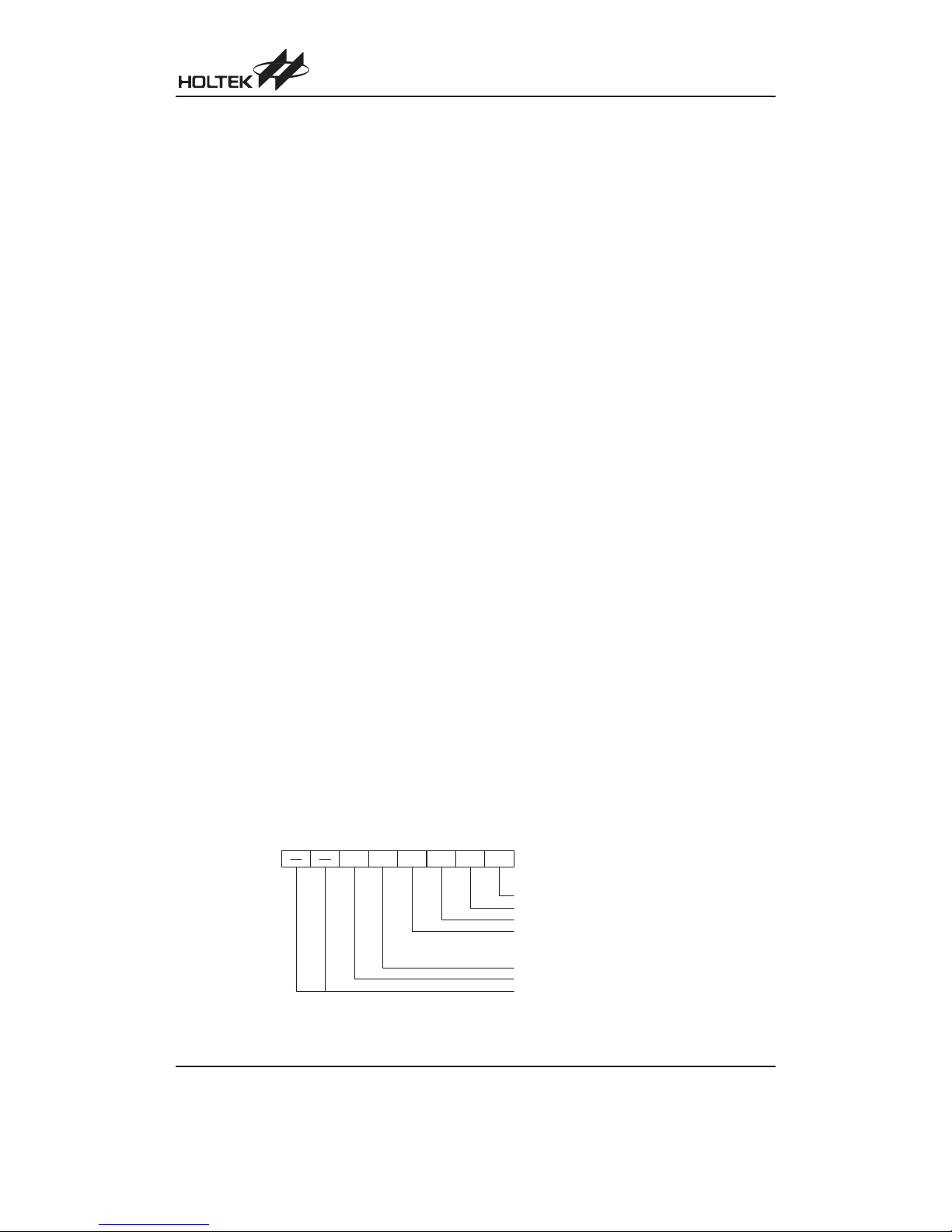
Input/Output Ports
Holtek microcontrollers offer considerable flexibility on
their I/Oports. With theinput or output designation of ev
-
ery pin fully under user program control, pull-high op
tions for all ports and wake-up options on certain pins,
the user is provided with an I/O structure to meet the
needs of a wide range of application possibilities.
Depending upon which device or package is chosen,
the microcontroller range provides from 13 to 23
bidirectional input/output lines labeled with port names
PA, PB, PC and PD. These I/O ports are mapped to the
RAM Data Memory with specific addresses as shown in
the Special Purpose Data Memory table. All of these I/O
ports can be used for input and output operations. For
input operation, these ports are non-latching, which
means the inputs must be ready at the T2 rising edge of
instruction ²MOV A,[m]², where m denotes the port ad
dress. For output operation, all the data is latched and
remains unchanged until the output latch is rewritten.
Pull-high Resistors
Many product applications require pull-high resistors for
their switch inputs usually requiring the use of an exter
nal resistor. To eliminate the need for these external re
sistors, all I/O pins, when configured as an input have
the capability of being connected to an internal pull-high
resistor. These pull-high resistors are selectable via
configuration options and are implemented using a
weak PMOS transistor.
Port A Wake-up
Each device has a HALT instruction enabling the
microcontroller to enter a Power Down Mode and preserve power, a feature that is important for battery and
other low-power applications. Various methods exist to
wake-up the microcontroller, one of which is to change
the logic condition on one of the Port Apins from high to
low. After a ²HALT² instruction forces the microcontroller
into entering a HALT condition, the processor will re
main idle or in a low-power state until the logic condition
of the selected wake-up pin on Port Achanges from high
to low. This function is especially suitable for applica
tions that can be woken up via external switches. Note
that each pin on Port A can be selected individually to
have this wake-up feature.
I/O Port Control Registers
Each I/O port has its own control register PAC, PBC,
PCC and PDC, to control the input/output configuration.
With this control register, each CMOS output or input
with or without pull-high resistor structures can be re
configured dynamicallyunder software control.Each pin
of the I/O ports is directly mapped to a bit in its associ
ated port control register. For the I/O pin to function as
an input, the corresponding bit of the control register
must be written as a ²1². This will then allow the logic
state of the input pin to be directly read by instructions.
When the corresponding bit of the control register is
written as a ²0², the I/O pin will be setup as a CMOS out
put. If the pin is currently setup as an output, instructions
can still be used to read the output register. However, it
should be noted that the program will in fact only read
the status of the output data latch and not the actual
logic status of the output pin.
Pin-shared Functions
The flexibility of the microcontroller range is greatly en
hanced by the use of pins that have more than one func
tion. Limited numbers of pins can force serious design
constraints on designers but by supplying pins with
multi-functions, many of these difficulties can be over
come. For some pins, the chosen function of the
multi-function I/O pins is set by configuration options
while for others the function is set by application pro
gram control.
·
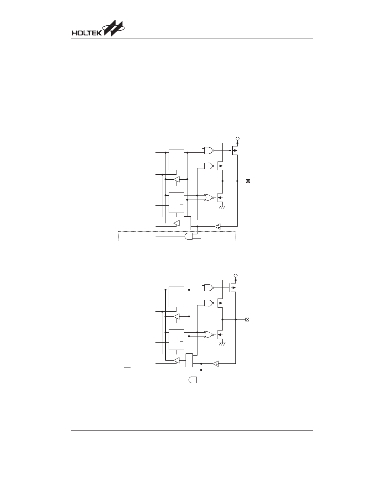
External Interrupt Input
The external interrupt pin INT
is pin-shared with the
I/O pin PA5. For applications not requiring an external
interrupt input, the pin-shared external interrupt pin
can be used as a normal I/O pin, however to do this,
the external interrupt enable bits in the INTC register
must be disabled.
·
External Timer Clock Input
The external timer pin TMR is pin-shared with the I/O
pin PA4. To configure it to operate as a timer input, the
corresponding control bits in the timer control register
must be correctly set. For applications that do not re
quire an external timer input, the pin can be used as a
normal I/O pin. Note that if used as a normal I/O pin
the timer mode control bits in the timer control register
must select the timer mode, which has an internal
clock source, to prevent the input pin from interfering
with the timer operation.
·
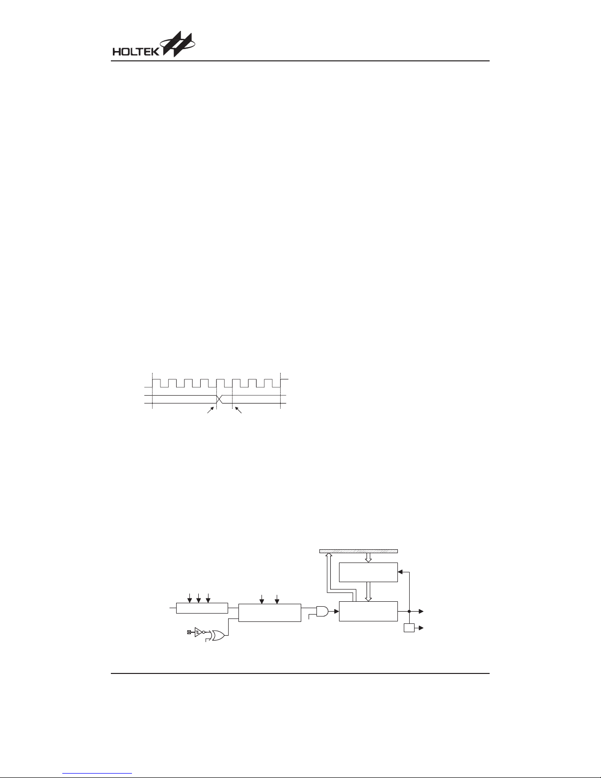
PFD Output
Each device contains a PFD function whose single
output is pin-shared with PA3. The output function of
this pin is chosen via a configuration option and re
mains fixed after the device is programmed. Note that
the corresponding bit of the port control register,
PAC.3, must setup the pin as an output to enable the
PFD output. If the PAC port control register has setup
the pin as an input, then the pin will function as a nor
mal logic input with the usual pull-high option, even if
the PFD configuration option has been selected.
Page 18
HT46R46/C46/R47/C47/R48A/C48A/R49
Rev. 1.41 18 December 30, 2008
·
PWM Outputs
All devices contain one or two PWM outputs pin
shared with pins PD0 and PD1. The PWM output
functions are chosen via configuration options and re
main fixed after the device is programmed. Note that
the corresponding bit or bits of the port control regis
ter, PDC, must setup the pin as an output to enable
the PWM output. If the PDC port control register has
setup the pin as an input, then the pin will function as a
normal logic input with the usual pull-high option, even
if the PWM configuration option has been selected.
·
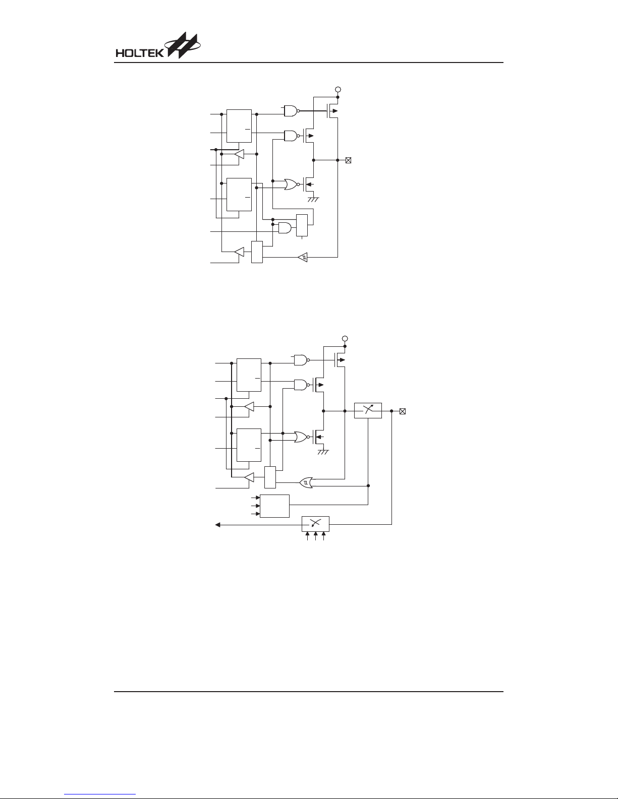
A/D Inputs
Each device has four A/D converter inputs. All of
these analog inputs are pin-shared with I/O pins on
Port B. If these pins are to be used as A/D inputs and
not as normal I/O pins then the corresponding bits in
the A/D Converter Control Register, ADCR, must be
properly set. There are no configuration options asso
ciated with the A/D function. If used as I/O pins, then
full pull-high resistor configuration options remain,
however if used as A/D inputs then any pull-high resis
tor options associated with these pins will be automat
ically disconnected.
V
D D
M
U
X
W a k e - u p O p t i o n
S y s t e m W a k e - u p
R e a d D a t a R e g i s t e r
C o n t r o l B i t
P u l l - H i g h
O p t i o n
D a t a B u s
W r i t e C o n t r o l R e g i s t e r
C h i p R e s e t
R e a
d C o n t r o l R e g i s t e r
W r i t e D a t a R e g i s t e r
D a t a B i t
I / O P i n
W e a k
P u l l - u p
D
Q
C K
S
Q
D
Q
C K
S
Q
P A o n l y
Non-pin-shared Function Input/Output Ports
V
D D
M
U
X
R e a d D a t a R e g i s t e r
C o n t r o l B i t
P u l l - H i g h
O p t i o n
D a t a B u s
W r i t e C o n t r o l R e g i s t e r
C h i p R e s e t
R e a d C o n t r o l R e g i s t e r
W r i t e D a t a R e g i s t e r
D a t a B
i t
I N T f o r P A 5 o n l y
T M R f o r P A 4 o n l y
P A 4 / T M R
P A 5 / I N T
W a k e - u p O p t i o n
S y s t e m W a k e - u p
W e a k
P u l l - u p
D
Q
C K
S
Q
D
Q
C K
S
Q
PA4/PA5 Input/Output Ports
Page 19
HT46R46/C46/R47/C47/R48A/C48A/R49
Rev. 1.41 19 December 30, 2008
V
D D
M
U
X
R e a d D a t a R e g i s t e r
C o n t r o l B i t
P u l l - H i g h
O p t i o n
D a t a B u s
W r i t e C o n t r o l R e g i s t e r
C h i p R e s e t
R e a d C o n t r o l R e g i s t e r
W r i t e D a t a R e g i s t e r
D a t a B
i t
P B 0 / A N 0 ~ P B 3 / A N 3
A C S 2 ~ A C S 0
T o A / D C o n v e r t e r
P C R 2
P C R 1
P C R 0
W e a k
P u l l - u p
A n a l o g
I n p u t
S e l e c t o r
D
Q
C K
S
Q
D
Q
C K
S
Q
PB Input/Output Ports
V
D D
P F D o r P W M W a v e f o r m
M
U
X
R e a d D a t a R e g i s t e r
C o n t r o l B i t
P u l l - H i g h
O p t i o n
D a t a B u s
W r i t e C o n t r o l R e g i s t e r
C h i p R e s e t
R e a d C o n t r o l R e g i s t e r
W r i t e D a t a R e g i s t e r
D a t a B
i t
P F D / P W M O p t i o n
M
U
X
W e a k
P u l l - u p
D
Q
C K
S
Q
D
Q
C K
S
Q
P A 3 / P F D
P D 0 / P W M
P D 0 / P W M 0
P D 1 / P W M 1
( H T 4 6 R 4 9 2 8 - p i n p a c k a g e o n l y )
PA3/PFD and PD/PWM Input/Output Ports
Page 20
HT46R46/C46/R47/C47/R48A/C48A/R49
Rev. 1.41 20 December 30, 2008
I/O Pin Structures
The following diagrams illustrate the I/O pin internal
structures. As the exact logical construction of the I/O
pin may differ from these drawings, they are supplied as
a guide only to assist with the functional understanding
of the I/O pins.
Programming Considerations
Within the user program, one of the first things to con
sider is port initialization. After a reset, all of the I/O data
and port control registers will be set high. This means
that all I/O pins will default to an input state, the level of
which depends on the other connected circuitry and
whether pull-high options have been selected. If the port
control registers, PAC, PBC, PCC and PDC, are then
programmed to setup some pins as outputs, these out
put pins will have an initial high output value unless the
associated port data registers, PA, PB, PC and PD, are
first programmed. Selecting which pins are inputs and
which are outputs can be achieved byte-wide by loading
the correct values into the appropriate port control regis
ter or by programming individual bits in the port control
register using the ²SET [m].i² and ²CLR [m].i² instruc
tions. Note that when using these bit control instruc
tions, a read-modify-write operation takes place. The
microcontroller must first read in the data on the entire
port, modify it to the required new bit values and then rewrite this data back to the output ports.
Port Ahas the additional capability of providing wake-up
functions. When the device is in the Power Down Mode,
various methods are available to wake the device up.
One of these is a high to low transition of any of the Port
A pins. Single or multiple pins on Port A can be setup to
have this function.
Note that some devices have different package types
which may result in some I/O pins not being bonded out.
If these pins are setup as inputs they may oscillate and
increase power consumption, especially notable if the
device isin the PowerDown Mode. It is therefore recom
-
mended that any unbonded pins should be setup as out
puts, or if setup as inputs, then they should be
connected to pull-high resistors.
Timer/Event Counters
The provision of timers form an important part of any
microcontroller giving the designer a means of carrying
out time related functions. Each device contains an in
ternal 8-bit count-up timer. With three operating modes,
the timers can be configured to operate as a general
timer, external event counter or as a pulse width mea
surement device. The provision of an internal 8-stage
prescaler to the timer clock circuitry gives added range
to the timer.
There are two registers related to the Timer/Event
Counter, TMR and TMRC. The TMR register is the reg
ister that contains the actual timing value. Writing to
TMR places an initial starting value in the Timer/Event
Counter preload register while reading TMR retrieves
the contents of the Timer/Event Counter. The TMRC
register is a Timer/Event Counter control register, which
defines the timer options, and determines how the timer
is to be used. The timer clock source can be configured
to come from the internal system clock source or from
an external clock on shared pin PA4/TMR.
Configuring the Timer/Event Counter Input Clock
Source
The internal timer¢s clock source can originate from either the system clock or from an external clock source.
The system clock input timer source is used when the
timer is in the timer mode or in the pulse width measure
ment mode. The internal timer clock also passes
through a prescaler, the value of which is conditioned by
the bits PSC0, PSC1 and PSC2.
An external clock source is used when the timer is in the
event counting mode, the clock source being provided
on pin-shared pin PA4/TMR. Depending upon the condi
tion of the TE bit, each high to low, or low to high transi
tion on the PA4/TMR pin will increment the counter by
one.
T 1 T 2
T 3 T 4
T 1 T 2
T 3 T 4
W r i t e t o P o r t R e a d f r o m P o r t
S y s t e m C l o c k
P o r t D a t a
Read/Write Timing
P A 4 / T M R I n p u t
T i m e r / E v e n t C o u n t e r
M o d e C o n t r o l
T O N
P r e l o a d R e g i s t e r
T i m e r / E v e n t C o u n t e r
D a t a B u s
R e l o a d
O v e r f l o w
t o I n t e r r u p t
2
8 - S t a g e P r e s c a l e r
P S C 2 ~ P S C 0
( 1 / 1 ~ 1 / 1 2 8 )
8 - B i t T i m e r / E v e n t C o u n t e r
T M 1 T M 0
f S Y S
P F D
¸
8-bit Timer/Event Counter Structure
Page 21

HT46R46/C46/R47/C47/R48A/C48A/R49
Rev. 1.41 21 December 30, 2008
Timer Register - TMR
The TMR register is an 8-bit special function register lo
cation within the special purpose Data Memory where
the actual timer value is stored. The value in the timer
registers increases by one each time an internal clock
pulse is received or an external transition occurs on the
PA4/TMR pin. The timer will count from the initial value
loaded by the preload register to the full count value of
FFH at which point the timer overflows and an internal
interrupt signal generated. The timer value will then be
reset with the initial preload register value and continue
counting. For a maximum full range count of 00H to FFH
the preload register must first be cleared to 00H. It
should be noted that after power-on the preload register
will be in an unknown condition. Note that if the
Timer/Event Counter is not running and data is written to
its preload register, this data will be immediately written
into the actual counter. However, if the counter is en
abled and counting, any new data written into the
preload register during this period will remain in the
preload register and will only be written into the actual
counter the next time an overflow occurs.
Timer Control Register - TMRC
The flexible features of the Holtek microcontroller
Timer/Event Counters enable them to operate in three
different modes, the options of which are determined by
the contents of the Timer Control Register TMRC. To
gether with the TMR register, these two registers control
the full operation of the Timer/Event Counters. Before
the timer can be used, it is essential that the TMRC reg
ister is fully programmed with the right data to ensure its
correct operation, a process that is normally carried out
during program initialisation.
To choose which of the three modes the timer is to oper
ate in, the timer mode, the event counting mode or the
pulse width measurement mode, bits TM0 and TM1
must be set to the required logic levels. The timer-on bit
TON or bit 4 of the TMRC register provides the basic
on/off control of the timer, setting the bit high allows the
counter to run, clearing the bit stops the counter. Bits
0~2 of the TMRC register determine the division ratio of
the input clock prescaler. The prescaler bit settings have
no effect if an external clock source is used. If the timer
is in the event count or pulse width measurement mode
the active transition edge level type is selected by the
logic level of the TE or bit 3 of the TMRC register.
T M R C R e g i s t e r
N o t i m p l e m e n t e d , r e a d a s " 0 "
b 7
E v e n t C o u n t e r A c t i v e E d g e S e l e c t
1 : c o u n t o n f a l l i n g e d g e
0 : c o u n t o n r i s i n g e d g e
T ET O NT M 0T M 1
T i m e r P r e s c a l e r R a t e S e l e c t
b 0
P S C 2
P S C 1 P S C 0
P S C 1
0
0
1
1
0
0
1
1
P S C 2
0
0
0
0
1
1
1
1
P S C 0
0
1
0
1
0
1
0
1
T i m e r R a t e
1 : 1
1 : 2
1 : 4
1 : 8
1 : 1 6
1 : 3 2
1 : 6 4
1 : 1 2 8
T i m e r / E v e n t C o u n t e r C o u n t i n g E n a b l e
1 : e n a b l e
0 : d i s a b l e
O p e r a t i n g M o d e S e l e c t
T M 1
0
0
1
1
T M 0
0
1
0
1
n o m o d
e a v a i l a b l e
e v e n t c o u n t e r m o d e
t i m e r m o d e
p u l s e w i d t h m e a s u r e m e n t m o d e
P u l s e W i d t h M e a s u r e m e n t A c t i v e E d g e S e l e c t
1 : s t a r t c o u n t i n g o n r i s i n g e d g e , s t o p o n f a l l i n g e d g e
0 : s t
a r t c o u n t i n g o n f a l l i n g e d g e , s t o p o n r i s i n g e d g e
Timer/Event Counter Control Register
Page 22

HT46R46/C46/R47/C47/R48A/C48A/R49
Rev. 1.41 22 December 30, 2008
Configuring the Timer Mode
In this mode, the timer can be utilised to measure fixed
time intervals, providing an internal interrupt signal each
time the counter overflows. To operate in this mode, bits
TM1 and TM0 of the TMRC register must be set to 1 and
0 respectively. In this mode, the internal clock is used as
the timer clock. The input clock frequency to the timer is
f
SYS
divided by the value programmed into the timer
prescaler, the value of which is determined by bits
PSC0~PSC2 of the TMRC register. The timer-on bit,
TON must be set high to enable the timer to run. Each
time an internal clock high to low transition occurs, the
timer increments by one. When the timer is full andover
flows, the timer will be reset to the value already loaded
into the preload register and continue counting. If the
timer interrupt is enabled, an interrupt signal will also be
generated. Thetimer interrupt canbe disabled by ensur
ing that the ETI bit in the INTC register is cleared to zero.
It should be noted that a timer overflow is one of the
wake-up sources.
Configuring the Event Counter Mode
In this mode, a number of externally changing logic
events, occurring on external pin PA4/TMR, can be re
corded by the internal timer. For the timer to operate in
the event counting mode, bits TM1 and TM0 of the
TMRC register must be set to 0 and 1 respectively. The
timer-on bit, TON must be set high to enable the timer to
count. With TE low, the counter will increment each time
the PA4/TMR pin receives a low to high transition. If the
TE bit is high, the counter will increment each time TMR
receives a high to low transition. As in the case of the
other two modes, when the counter is full and overflows,
the timer will be reset to the value already loaded into
the preload register and continue counting. If the timer
interrupt is enabled, an interrupt signal will also be gen
erated. The timer interrupt can be disabled by ensuring
that the ETI bit in the INTC register is cleared to zero. To
ensure that the external pin PA4/TMR is configured to
operate asan event counter input pin, two things have to
happen. The first is to ensure that the TM0 and TM1 bits
place the timer/event counter in the event counting
mode, the second is to ensure that the port control regis
ter configures the pin as an input. It should be noted that
a timer overflow is one of the wake-up sources. Also in
the Event Counting mode, the Timer/Event Counter will
continue to record externally changing logic events on
the timer input pin, even if the microcontroller is in the
Power Down Mode. As a result when the timer over
flows it will generate a wake-up and if the interrupts are
enabled also generate a timer interrupt signal.
Configuring the Pulse Width Measurement Mode
In this mode, the width of external pulses applied to the
pin-shared external pin PA4/TMR can be measured. In
the Pulse Width Measurement Mode, the timer clock
source is supplied by the internal clock. For the timer to
operate in this mode, bits TM0 and TM1 must both be
set high. If the TE bit is low, once a high to low transition
has been received on the PA4/TMR pin, the timer will
start counting until the PA4/TMR pin returns to its origi
nal high level. At this point the TON bit will be automati
cally reset to zero and the timer will stop counting. If the
TE bit is high, the timer will begin counting once a low to
high transition has been received on the PA4/TMR pin
and stop counting when the PA4/TMR pin returns to its
original lowlevel. As before,the TON bit will be automat
ically reset to zero and the timer will stop counting. It is
important to note that in the Pulse Width Measurement
Mode, the TON bit is automatically reset to zero when
the external control signal on the external timer pin returns to its original level, whereas in the other two
modes the TON bit can only be reset to zero under program control. The residual value in the timer, which can
now be read by the program, therefore represents the
length of the pulse received on pin PA4/TMR. As the
TON bit has now been reset any further transitions on
the PA4/TMR pin will be ignored. Not until the TON bit is
again set high by the program can the timer begin fur
ther pulse width measurements. In this way single shot
pulse measurements can be easily made. It should be
noted that in this mode the counter is controlled by logi
cal transitions on the PA4/TMR pin and not by the logic
level.
I n c r e m e n t
T i m e r C o n t r o l l e r
P r e s c a l e r O u t p u t
T i m e r + 1
T i m e r + 2
T i m e r + N T i m e r + N + 1
Timer Mode Timing Chart
T i m e r + 2
E x t e r n a l E v e n t
I n c r e m e n t
T i m e r C o u n t e r
T i m e r + 3T i m e r + 1
Event Counter Mode Timing Chart
Page 23
HT46R46/C46/R47/C47/R48A/C48A/R49
Rev. 1.41 23 December 30, 2008
As in the case of the other two modes, when the counter
is full and overflows, the timer will be reset to the value
already loaded into the preload register. If the timer in
-
terrupt is enabled, an interrupt signal will also be gener
ated. To ensure that the external pin PA4/TMR is
configured to operate as a pulse width measuring input
pin, two things have to happen. The first is to ensure that
the TM0 and TM1 bits place the timer/event counter in
the pulse width measuring mode, the second is to en
sure that the port control register configures the pin as
an input. It should be noted that a timer overflow is one
of the wake-up sources.
Programmable Frequency Divider - PFD
The PFD output is pin-shared with the I/O pin PA3. The
PFD function is selected via configuration option, how
ever, if not selected, the pin can operate as a normal I/O
pin. The timer overflow signal is the clock source for the
PFD circuit. The output frequency is controlled by load
ing the required values into the timer prescaler registers
to give the required division ratio. The counter, driven by
the system clock which is divided by the prescaler value,
will begin to count-up from this preload register value
until full, at which point an overflow signal is generated,
causing the PFD output to change state. The counter
will then be automatically reloaded with the preload reg
ister value and continue counting-up.
For the PFD output to function, it is essential that the
corresponding bit of the Port A control register PAC bit 3
is setup as an output. If setup as an input the PFD output
will not function, however, the pin can still be used as a
normal input pin. The PFD output will only be activated if
bit PA3 is set to ²1². This output data bit is used as the
on/off control bit for the PFD output. Note that the PFD
output will be low if the PA3 output data bit is cleared to
²0².
Using this method of frequency generation, and if a
crystal oscillator is used for the system clock, very pre
-
cise values of frequency can be generated.
Prescaler
Bits PSC0~PSC2 of the TMRC register can be used to
define the pre-scaling stages of the internal clock
sources of the Timer/Event Counter. The Timer/Event
Counter overflow signal can be used to generate signals
for the PFD and Timer Interrupt.
I/O Interfacing
The Timer/Event Counter, when configured to run in the
event counter or pulse width measurement mode, re
-
quire the use of the external PA4/TMR pin for correct op
eration. As this pin is a shared pin it must be configured
correctly to ensure it is setup for use as a Timer/Event
Counter input and not as a normal I/O pin. This is imple
mented by ensuring that the mode select bits in the
Timer/Event Counter control register, select either the
event counter or pulse width measurement mode. Addi
tionally the Port Control Register PAC bit 4 must be set
high to ensure that the pin is setup as an input. Any
pull-high resistor configuration option on this pin will remain valid even if the pin is used as a Timer/Event
Counter input.
+ 1 + 2 + 3 + 4
T i m e r
E x t e r n a l T M R
P i n I n p u t
T O N ( w i t h T E = 0 )
P r e s c a l e r O u t p u t
I n c r e m e n t
T i m e r C o u n t e r
P r e s c a l e r O u t p
u t i s s a m p l e d a t e v e r y f a l l i n g e d g e o f T 1 .
Pulse Width Measure Mode Timing Chart
T i m e r O v e r f l o w
P F D C l o c k
P A 3 D a t a
P F D O u t p u t a t P A 3
PFD Output Control
Page 24

HT46R46/C46/R47/C47/R48A/C48A/R49
Rev. 1.41 24 December 30, 2008
Programming Considerations
When configured to run in the timer mode, the internal
system clock is used as the timer clock source and is
therefore synchronized with the overall operation of the
microcontroller. In this mode when the appropriate timer
register is full, the microcontroller will generate an internal
interrupt signal directing the program flow to the respec
-
tive internal interrupt vector. For the pulse width mea
surement mode, the internal system clock is also used as
the timer clock source but the timer will only run when the
correct logic condition appears on the external timer input
pin. As this is an external event and not synchronized
with the internal timer clock, the microcontroller will only
see this external event when the next timer clock pulse
arrives. As a result, there may be small differences in
measured values requiring programmers to take this into
account during programming. The same applies if the
timer is configured to be in the event counting mode,
which again is an external event and not synchronized
with the internal system or timer clock.
When the Timer/Event Counter is read, or if data is writ
ten to the preload register, the clock is inhibited to avoid
errors, however as this may result in a counting error, this
should be taken into account by the programmer. Care
must be taken to ensure that the timers are properly in
itialised before using them for the first time. The associated timer enable bits in the interrupt control register must
be properly set otherwise the internal interrupt associated
with the timer will remain inactive. The edge select, timer
mode and clock source control bits in timer control register must also be correctly set to ensure the timer is properly configured for the required application. It is also
important to ensure that an initial value is first loaded into
the timer registers before the timer is switched on; this is
because after power-on the initial values of the timer reg
isters are unknown. After the timer has been initialised
the timer can be turned on and off by controlling the en
able bit in the timer control register. Note that setting the
timer enable bit high to turn the timer on, should only be
executed after the timer mode bits have been properly
setup. Setting the timer enable bit high together with a
mode bit modification, may lead to improper timer oper
ation if executed as a single timer control register byte
write instruction.
When the Timer/Event counter overflows, its corre
sponding interrupt request flag in the interrupt control
register will be set. If the timer interrupt is enabled this
will in turn generate an interrupt signal. However irre
spective of whether the interrupts are enabled or not, a
Timer/Event counter overflow will also generate a
wake-up signal if the device is in a Power-down condi
tion. This situation may occur if the Timer/Event Counter
is in the Event Counting Mode and if the external signal
continues to change state. In such a case, the
Timer/Event Counter will continue to count these exter
nal events and if an overflow occurs the device will be
woken up from its Power-down condition. To prevent
such a wake-up from occurring, the timer interrupt re
quest flag should first be set high before issuing the
HALT instruction to enter the Power Down Mode.
Timer Program Example
This program example shows how the Timer/Event
Counter registers are setup, along with how the interrupts are enabled and managed. Note how the
Timer/Event Counter is turned on, by setting bit 4 of the
Timer Control Register. The Timer/Event Counter can
be turned off in a similar way by clearing the same bit.
This example program sets the Timer/Event Counter to
be in the timer mode, which uses the internal system
clock as the clock source.
org 04h ; external interrupt vector
reti
org 08h ; Timer/Event Counter interrupt vector
jmp tmrint ; jump here when Timer overflows
:
org 20h ; main program
;internal Timer/Event Counter interrupt routine
tmrint:
:
; Timer/Event Counter main program placed here
:
reti
:
:
begin:
;setup Timer registers
mov a,09bh ; setup Timer preload value
mov tmr,a;
mov a,081h ; setup Timer control register
mov tmrc,a ; timer mode and prescaler set to /2
; setup interrupt register
mov a,005h ; enable master interrupt and timer interrupt
mov intc,a
set tmrc.4 ; start Timer - note mode bits must be previously setup
Page 25

HT46R46/C46/R47/C47/R48A/C48A/R49
Rev. 1.41 25 December 30, 2008
Pulse Width Modulator
Each microcontroller in the Cost-effective A/D Type
MCU series contains either one or two Pulse Width
Modulation, PWM, outputs. Useful for such applications
such as motor speed control, the PWM function pro
vides outputswith a fixedfrequency but with a duty cycle
that can be varied by setting particular values into the
corresponding PWM register.
Device Channels
PWM
Mode
Output
Pins
Register
Name
HT46R49 2 6+2
PD0/
PD1
PWM0/
PWM1
Other
Devices
1 6+2 PD0 PWM
For devices with one PWM output, a single register, lo
cated inthe Data Memoryis assigned to the Pulse Width
Modulator and is known as the PWM register. For de
vices with two PWM outputs, two registers are provided
and are known as PWM0 and PWM1. It is in these regis
ters, that the 8-bit value, which represents the overall
duty cycle of one modulation cycle of the output wave
form, should be placed. To increase the PWM modula
tion frequency, each modulation cycle is modulated into
four individual modulation sub-sections, known as the
6+2 mode. Note that it is only necessary to write the required modulation value into the corresponding PWM
register as the subdivision of the waveform into its
sub-modulation cycles is implemented automatically
within the microcontroller hardware. For all devices, the
PWM clock source is the system clock f
SYS
.
This method of dividing the original modulation cycle
into a further 4 sub-cycles enables the generation of
higher PWM frequencies, which allow a wider range of
applications to be served. As long as the periods of the
generated PWM pulses are less than the time constants
of the load, the PWM output will be suitable as such long
time constant loads will average out the pulses of the
PWM output. The difference between what is known as
the PWM cycle frequency and the PWM modulation fre
quency should be understood. As the PWM clock is the
system clock, f
SYS
, and as the PWM value is 8-bits wide,
the overall PWM cycle frequency is f
SYS
/256, while the
PWM modulation frequency for the 6+2 mode of opera
tion will be f
SYS
/64.
PWM
Modulation
Frequency
PWM Cycle
Frequency
PWM Cycle
Duty
f
SYS
/64 f
SYS
/256
(PWM register
value)/256
6+2 PWM Mode
Each full PWM cycle, as it is controlled by an 8-bit PWM,
PWM0 or PWM1 register, has 256 clock periods. How
ever, in the 6+2 PWM Mode, each PWM cycle is subdi
vided into four individual sub-cycles known as
modulation cycle 0~modulation cycle 3, denoted as ²i²
in the table. Each one of these four sub-cycles contains
64 clock cycles. In this mode, a modulation frequency
increase by a factor of four is achieved. The 8-bit PWM,
PWM0 or PWM1 register value, which represents the
overall duty cycle of the PWM waveform, is divided into
two groups. The first group which consists of bit2~bit7 is
denoted here as the DC value. The second group which
consists of bit0~bit1 is known as the AC value. In the
6+2 PWM mode, the duty cycle value of each of the four
modulation sub-cycles is shown in the following table.
Parameter AC (0~3)
DC
(Duty Cycle)
Modulation cycle i
(i=0~3)
i<AC
DC 164+
i³AC
DC
64
6+2 Mode Modulation Cycle Values
Page 26
HT46R46/C46/R47/C47/R48A/C48A/R49
Rev. 1.41 26 December 30, 2008
The following diagram illustrates the waveforms associ
-
ated with the 6+2 mode of PWM operation. It is impor
tant to note how the single PWM cycle is subdivided into
4 individual modulation cycles, numbered from 0~3 and
how the AC value is related to the PWM value.
PWM Output Control
On all devices, the PWM outputs are pin-shared with
pins PD0 and PD1. To operate as PWM outputs and not
as I/O pins, the correct PWM configuration options must
be selected. A ²0² must also be written to the corre
sponding bits in the I/O port control register PDC to en
sure that the required PWM output pin is setup as an
output. After these two initial steps have been carried
out, and of course after the required PWM value has
been written into the PWM register, writing a ²1² to the
corresponding bit in the PD output data register will en
-
able the PWM data to appear on the pin. Writing a ²0² to
the corresponding bit in the PD output data register will
disable the PWM output function and force the output
low. In this way, the Port D data output register can be
used as an on/off control for the PWM function. Note
that if the configuration options have selected the PWM
function, but a ²1² has been written to its corresponding
bit in the PDC control register to configure the pin as an
input, then the pin can still function as a normal input
line, with pull-high resistor options.
PWM Programming Example
The following sample program shows how the PWM outputs are setup and controlled. Before use the corresponding
PWM output configuration options must first be selected.
mov a,64h ; setup PWM value of 100 decimal which is 64H
mov pwm,a
clr pdc.0 ; setup pin PD0 as an output
set pd.0 ; PD.0=1; enable the PWM output
::
::
clr pd.0 ; disable the PWM output - PD0 will remain low
f
S Y S
/ 2
P W M
[ P W M ] = 1 0 0
[ P W M ] = 1 0 1
P W M
[ P W M ] = 1 0 2
P W M
[ P W M ] = 1 0 3
P W M
P W M c y c l e : 2 5 6 / f
S Y S
2 5 / 6 4
2 6 / 6 4
2 6 / 6 4
2 6 / 6 4
2 5 / 6 4 2 5 / 6 4 2 5 / 6 4
2 5 / 6 4
2 5 / 6 4
2 5 / 6 4
2 5 / 6 4
2 6 / 6 4
2 6 / 6 4
2 5 / 6 4
2 5 / 6 4
2 6 / 6 4 2 5 / 6 4
2 6 / 6 4
2 6 / 6 4
2 6 / 6 4
M o d u l a t i o n c y c l e 0
P W M m o d u l a t i o n p e r i o d : 6 4 / f
S Y S
M o d u l a t i o n c y c l e 1 M o d u l a t i o n c y c l e 2 M o d u l a t i o n c y c l e 3 M o d u l a t i o n c y c l e 0
6+2 PWM Mode
P W M , P W M 0 , P W M 1 R e g i s t e r
b 7 b 0
A C v a l u e
D C v a l u e
Pulse Width Modulation Registers
Page 27

HT46R46/C46/R47/C47/R48A/C48A/R49
Rev. 1.41 27 December 30, 2008
Analog to Digital Converter
The need to interface to real world analog signals is a
common requirement for many electronic systems.
However, to properly process these signals by a
microcontroller, they must first be converted into digital
signals by A/D converters. By integrating the A/D con
version electronic circuitry into the microcontroller, the
need for external components is reduced significantly
with the corresponding follow-on benefits of lower costs
and reduced component space requirements.
A/D Overview
Each of the devices contains a 4-channel analog to digi
tal converter which can directly interface to external an
alog signals, such as that from sensors or other control
signals and convert these signals directly into either an
8-bit or 9-bit digital value.
Device
Input
Channels
Conversion
Bits
Input Pins
HT46R46 4 8 PB0~PB3
HT46R47 4 9 PB0~PB3
HT46R48A 4 9 PB0~PB3
HT46R49 4 9 PB0~PB3
The following diagram shows the overall internal structure of the A/D converter, together with its associated
registers.
A/D Converter Data Registers - ADR, ADRL, ADRH
For the HT46R46 device, which has an 8-bit A/D converter, a single register, known as ADR, is used to store
the 8-bit analog to digital conversion value. For the remaining devices, which have a 9-bit A/D converter, two
registers are required, a high byte register, known as
ADRH, and a low byte register, known as ADRL. After
the conversion process takes place, these registers can
be directly read by the microcontroller to obtain the digit
ised conversion value. For devices which use two A/D
Converter Data Registers, note that only the high byte
register ADRH utilises its full 8-bit contents. The low
byte register utilises only 1 bit of its 8-bit contents as it
contains onlythe lowest bit of the 9-bit converted value.
In the following tables, D0~D8 are the A/D conversion
data result bits.
Register
Bit7Bit6Bit5Bit4Bit3Bit2Bit1Bit
0
ADR D7 D6 D5 D4 D3 D2 D1 D0
A/D Data Register - HT46R46
Register
Bit7Bit6Bit5Bit4Bit3Bit2Bit1Bit
0
ADRL
D0
¾¾¾¾¾¾¾
ADRH
D8 D7 D6 D5 D4 D3 D2 D1
A/D Data Register - Other Devices
A/D Converter Control Register - ADCR
To control the function and operation of the A/D con
verter, a control register known as ADCR is provided.
This 8-bit register defines functions such as the selec
tion of which analog channel is connected to the internal
A/D converter, which pins are used as analog inputs and
which are used as normal I/Os as well as controlling the
start function and monitoring the A/D converter end of
conversion status.
One section of this register contains the bits
ACS2~ACS0 whichdefine the channel number. As each
of the devices contains only one actual analog to digital
converter circuit, each of the individual 4 analog inputs
must be routed to the converter. It is the function of the
ACS2~ACS0 bits in the ADCR register to determine
which analog channel is actually connected to the inter
nal A/D converter. Note that the ACS2 bit must always
be assigned a zero value.
A D C S o u r c e
f
S Y S
/ 2
¸
N
A C S R R e g i s t e r
A D C
V
D D
P B 0 / A N 0
P B 1 / A N 1
P B 2 / A N 2
P B 3 / A N 3
A / D r e f e r e n c e v o l t a g e
P C R 0 ~ P C R 2
A D C S 0 ~ A D C S 2
S T A R T
E O C B
A D C R
R e g i s t e r
P i n C o n f i g u r a t i o n
B i t s
C h a n n e l S e l e c t
B i t s
S t a r t B i t
C l o c k D i v i d e
R a t i o
E n d o f
C o n v e r s i o n B i t
A D R
o r
A D R L
A D R H
A / D D a t a
R e g i s t e r s
A/D Converter Structure
Page 28

HT46R46/C46/R47/C47/R48A/C48A/R49
Rev. 1.41 28 December 30, 2008
The ADCR control register also contains the
PCR2~PCR0 bits which determine which pins on Port B
are used as analog inputs for the A/D converter and
which pins are to be used as normal I/O pins. If the 3-bit
address on PCR2~PCR0 has a value of ²100² or higher,
then all four pins, namely AN0, AN1, AN2 and AN3 will all
be set as analog inputs. Note that if the PCR2~PCR0 bits
are all set to zero, then all the Port B pins will be setup as
normal I/Os and the internal A/D converter circuitry will be
powered off to reduce the power consumption.
The START bit in the ADCR register is used to start and
reset the A/D converter. When the microcontroller sets
this bit from low to high and then low again, an analog to
digital conversion cycle will be initiated. When the
START bit is brought from low to high but not low again,
the EOCB bit in the ADCR register will be set to a ²1²
and the analog to digital converter will be reset. It is the
START bit that is used to control the overall on/off opera
-
tion of the internal analog to digital converter.
The EOCB bit in the ADCR register is used to indicate
when the analog to digital conversion process is com
-
plete. This bit will be automatically set to ²0² by the
microcontroller after a conversion cycle has ended. In
addition, the corresponding A/D interrupt request flag
will be set in the interrupt control register, and if the inter
rupts are enabled, an appropriate internal interrupt signal will be generated. This A/D internal interrupt signal
will direct the program flow to the associated A/D inter-
nal interrupt address for processing. If the A/D internal
interrupt is disabled, the microcontroller can be used to
poll the EOCB bit in the ADCR register to check whether
it has been cleared as an alternative method of detect
-
ing the end of an A/D conversion cycle.
A/D Converter Clock Source Register - ACSR
The clock source for the A/D converter, which originates
from the system clock f
SYS
, is first divided by a division
ratio, the value of which is determined by the ADCS1
and ADCS0 bits in the ACSR register.
Although the A/D clock source is determined by the sys
-
tem clock f
SYS
, and by bits ADCS1 and ADCS0, there are
some limitations on the maximum A/D clock source speed
that can be selected. As the minimum value of permissible
A/D clock period, t
AD
,is0.5ms for the HT46R46, device,
and 1ms for the other devices, care must be taken for sys
tem clock speeds in excess of 2MHz.With the exception of
the HT46R46 device, for system clock speeds in excess of
2MHz, the ADCS1 and ADCS0 bits should not be set to
²00². For the HT46R46 device, for system clock speeds in
excess of 4MHz, the ADCS1 and ADCS0 bits should not
be set to ²00². Doing so will give A/D clock periods that are
less than the minimum A/D clock period which may result
in inaccurate A/D conversion values. Refer to the following
table for examples, where values marked with an asterisk
* show where, depending upon the device, special care
must be taken, as the values may be less than the specified minimum A/D Clock Period.
A D C R R e g i s t e r
S e l e c t A / D c h a n n e l
b 7 b 0
S T A R T
P C R 2
P C R 1 P C R 0
A C S 2 A C S 1 A C S 0
A C S 1
0
0
1
1
X
A C S 2
0
0
0
0
1
A C S 0
0
1
0
1
X
: A N 0
: A N 1
: A N 2
: A N 3
: u n d e f i n e d , m u s t n o t b e u s e d
P o r t B A / D c
h a n n e l c o n f i g u r a t i o n s
P C R 2
0
0
0
0
1
P C R 1
0
0
1
1
X
P C R 0
0
1
0
1
X
: P o r t B A / D c h a n n e l s - a l l o f f
: P B 0 e n a b l e d a s A N 0
: P B 0 ~ P B 1 e n a b l e d a s A N 0 ~ A N 1
: P B 0 ~ P B 2 e n a b l e d a s A N 0 ~ A N 2
: P B 0 ~ P B 3 e n a b l e d a s A N 0 ~ A N 3
E n d o f A / D c o
n v e r s i o n f l a g
1 : n o t e n d o f A / D c o n v e r s i o n - A / D c o n v e r s i o n w a i t i n g o r i n p r o g r e s s
0 : e n d o f A / D c o n v e r
s i o n - A / D c o n v e r s i o n e n d e d
S t a r t t h e A / D c o n v e r s i o n
0
®
1
®
0 : S t a r t
0
®
1 : R e s e t A / D c o n v e r t e r a n d s e t E O C B t o " 1 "
E O C B
A/D Converter Control Register
A C S R R e g i s t e r
S e l e c t A / D c o n v e r t e r c l o c k s o u r c e
b 7 b 0
T E S T
A D C S 1 A D C S 0
A D C S 1
0
0
1
1
A D C S 0
0
1
0
1
: s y s t e m c l o c k / 2
: s y s t e m c l o c k / 8
: s y s t e m c l o c k / 3 2
: u n d e f i n e d
N o t i m p l e m e n t e d , r e a d a s " 0 "
F o r t e s t m o d e u s e o n l y
A/D Converter Clock Source Register
Page 29

HT46R46/C46/R47/C47/R48A/C48A/R49
Rev. 1.41 29 December 30, 2008
f
SYS
A/D Clock Period (tAD)
ADCS1, ADCS0=00
(f
SYS
/2)
ADCS1, ADCS0=01
(f
SYS
/8)
ADCS1, ADCS0=10
(f
SYS
/32)
ADCS1, ADCS0=11
1MHz
2ms8ms32ms
Undefined
2MHz
1ms4ms16ms
Undefined
4MHz 500ns*
2ms8ms
Undefined
8MHz 250ns*
1ms4ms
Undefined
A/D Clock Period Examples
A/D Input Pins
All of the A/D analog input pins are pin-shared with the
I/O pins on Port B. Bits PCR2~PCR0 in the ADCR regis
-
ter, not configuration options, determine whether the in
put pins are setup as normal Port B input/output pins or
whether they are setup as analog inputs. In this way, pins
can be changed under program control to change their
function from normal I/O operation to analog inputs and
vice versa. Pull-high resistors, which are setup through
configuration options, apply to the input pins only when
they are used as normal I/O pins, if setup as A/D inputs
the pull-high resistors will be automatically disconnected.
Note that it is not necessary to first setup the A/D pin as
an input in the PBC port control register to enable the A/D
input, when the PCR2~PCR0 bits enable an A/D input,
the status of the port control register will be overridden.
The VDD power supply pin is used as the A/D converter
reference voltage, and as such analog inputs must not be
allowed to exceed this value. Appropriate measures
should also be taken to ensure that the VDD pin remains
as stable and noise free as possible.
Initialising the A/D Converter
The internal A/D converter must be initialised in a spe
cial way. Each time the Port B A/D channel selection bits
are modified by the program, the A/D converter must be
re-initialised. If the A/D converter is not initialised after
the channel selection bits are changed, the EOCB flag
may have an undefined value, which may produce a
false end of conversion signal. To initialise the A/D con
verter after the channel selection bits have changed,
then, within a time frame of one to ten instruction cycles,
the START bit in the ADCR register must first be set high
and then immediately cleared to zero. This will ensure
that the EOCB flag is correctly set to a high condition.
Summary of A/D Conversion Steps
The following summarizes the individual steps that
should be executed in order to implement an A/D con
version process.
·
Step 1
Select the required A/D conversion clock by correctly
programming bits ADCS1 and ADCS0 in the ACSR
register.
·
Step 2
Select whichchannel is tobe connected tothe internal
A/D converter by correctly programming the
ACS2~ACS0 bits which are also contained in the
ADCR register.
·
Step 3
Select which pins on Port B are to be used as A/D in
puts and configure them as A/D input pins by correctly
programming the PCR2~PCR0 bits in the ADCR reg
ister. Note that this step can be combined with Step 2
into a single ADCR register programming operation.
·
Step 4
If the interrupts are to be used, the interrupt control
registers must be correctly configured to ensure the
A/D converter interrupt function is active. The master
interrupt control bit, EMI, in the INTC interrupt control
register must be set to ²1² and the A/D converter interrupt bit, EADI, in the INTC register must also be set to
²1².
·
Step 5
The analog to digital conversion process can now be
initialised by setting the START bit in the ADCR regis
ter from ²0² to ²1² and then to ²0² again. Note that this
bit should have been originally set to ²0².
·
Step 6
To check when the analog to digital conversion pro
cess is complete, the EOCB bit in the ADCR register
can be polled. The conversion process is complete
when this bit goes low. When this occurs the A/D data
registers ADRL and ADRH can be read to obtain the
conversion value. As an alternative method if the in
terrupts are enabled and the stack is not full, the pro
gram can wait for an A/D interrupt to occur.
Note: When checking for the end of the conversion
process, if the method of polling the EOCB bit in
the ADCR register is used, the interrupt enable
step above can be omitted.
Page 30
HT46R46/C46/R47/C47/R48A/C48A/R49
Rev. 1.41 30 December 30, 2008
The following timing diagram shows graphically the various stages involved in an analog to digital conversion process
and its associated timing.
The setting up and operation of the A/D converter func
tion is fully under the control of the application program as
there are no configuration options associated with the
A/D converter. After an A/D conversion process has been
initiated by the application program, the microcontroller
internal hardware will begin to carry out the conversion,
during which time the program can continue with other
functions. The time taken for the A/D conversion is dependent upon the device chosen and is a function of the
A/D clock period t
AD
as shown in the table.
Device A/D Conversion Time
HT46R46 64t
AD
Other Devices 76t
AD
A/D Conversion Time
Programming Considerations
When programming, special attention must be given to
the A/D channel selection bits in the ADCR register. If
these bits are all cleared to zero no external pins will be
selected for use as A/D input pins allowing the pins to be
used as normal I/O pins. When this happens the power
supplied to the internal A/D circuitry will be reduced resulting in a reduction of supply current. This ability to reduce power by turning off the internal A/D function by
clearing the A/D channel selection bits may be an important consideration in battery powered applications.
Another important programming consideration is that
when the A/D channel selection bits change value the
A/D converter must be re-initialised. This is achieved by
pulsing the START bit in the ADCR register immediately
after the channel selection bits have changed state. The
exception to this is where the channel selection bits are
all cleared, in which case the A/D converter is not re
-
quired to be re-initialised.
0 0 0 B
0 0 0 B
0 1 1 B
0 1 0 B
S T A R T
E O C B
P C R 2 ~
P C R 0
A C S 2 ~
A C S 0
P o w e r - o n
R e s e t
E n d o f A / D
c o n v e r s i o n
1 : D e f i n e P B c o n f i g u r a t i o n
2 : S e l e c t a n a l o g c h a n n e l
S t a r t o f A / D
c o n v e r s i o n
R e s e t A / D
c o n v e r t e r
0 0 0 B
S t a r t o f A / D
c o n v e r s i o n
R e s e t A / D
c o n v e r t e r
0 0 0 B
1 . P B p o r t s e t u p a s I / O s
2 . A / D c o n v e r t e r i s p o w e r e d o f f
t o r e d u c e p o w e r c o n s u m p t i o n
1 0 0 B
0 0 1 B
S t a r t o f A / D
c o n v e r s i o n
R e s e t A / D
c o n v e r t e r
D o n ' t c a r e
E n d o f A / D
c o n v e r s i o n
E n d o f A / D
c o n v e r s i o n
S T A R T b i t s e t h i g h w i t h i n o n e t o t e n i n s t r u c t i o n c y c l e s a f t e r t h e P C R 0 ~ P C R 2 b i t s c h a n g e s t a t e
A / D c l o c k m u s t b e f
S Y S
/ 2 , f
S Y S
/ 8 o r f
S Y S
/ 3 2
N o t e :
A / D s a m p l i n g t i m e A / D s a m p l i n g t i m e
A / D s a m p l i n g t i m e
3 2 t
A D
3 2 t
A D
3 2 t
A D
t
A D C
A / D c o n v e r s i o n t i m e A / D c o n v e r s i o n t i m e A / D c o n v e r s i o n t i m e
t
A D C
t
A D C
A/D Conversion Timing
Page 31

HT46R46/C46/R47/C47/R48A/C48A/R49
Rev. 1.41 31 December 30, 2008
A/D Programming Example
The following two programming examples illustrate how to setup and implement an A/D conversion. In the first exam
ple, the method of polling the EOCB bit in the ADCR register is used to detect when the conversion cycle is complete,
whereas in the second example, the A/D interrupt is used to determine when the conversion is complete.
Example: using an EOCB polling method to detect the end of conversion for the HT46R46
clr EADI ; disable ADC interrupt
mov a,00000001B
mov ACSR,a ; setup the ACSR register to select f
SYS
/8 as
; the A/D clock
mov a,00100000B ; setup ADCR register to configure Port PB0~PB3
; as A/D inputs
mov ADCR,a ; and select AN0 to be connected to the A/D
; converter
:
: ; As the Port B channel bits have changed the
; following START
; signal (0-1-0) must be issued within 10
; instruction cycles
:
Start_conversion:
clr START
set START ; reset A/D
clr START ; start A/D
Polling_EOC:
sz EOCB ; poll the ADCR register EOCB bit to detect end
; of A/D conversion
jmp polling_EOC ; continue polling
mov a,ADR ; read conversion result value from the ADR
; register
mov adr_buffer,a ; save result to user defined memory
:
:
jmp start_conversion ; start next A/D conversion
Page 32

HT46R46/C46/R47/C47/R48A/C48A/R49
Rev. 1.41 32 December 30, 2008
Example: using an interrupt method to detect the end of conversion for the HT46R46
clr EADI ; disable ADC interrupt
mov a,00000001B
mov ACSR,a ; setup the ACSR register to select fSYS/8 as
; the A/D clock
mov a,00100000B ; setup ADCR register to configure Port PB0~PB3
; as A/D inputs
mov ADCR,a ; and select AN0 to be connected to the A/D
; converter
:
; As the Port B channel bits have changed the
; following START
; signal (0-1-0) must be issued within 10
; instruction cycles
:
Start_conversion:
clr START
set START ; reset A/D
clr START ; start A/D
clr ADF ; clear ADC interrupt request flag
set EADI ; enable ADC interrupt
set EMI ; enable global interrupt
:
:
:
; ADC interrupt service routine
ADC_ISR:
mov acc_stack,a ; save ACC to user defined memory
mov a,STATUS
mov status_stack,a ; save STATUS to user defined memory
:
:
mov a,ADR ; read conversion result value from the ADR
; register
mov adr_buffer,a ; save result to user defined register
:
:
EXIT_INT_ISR:
mov a,status_stack
mov STATUS,a ; restore STATUS from user defined memory
mov a,acc_stack ; restore ACC from user defined memory
reti
Page 33

HT46R46/C46/R47/C47/R48A/C48A/R49
Rev. 1.41 33 December 30, 2008
A/D Transfer Function
As the HT46R46 device contain an 8-bit A/D converter,
their full-scale converted digitized value is equal to
0FFH. Since the full-scale analog input value is equal to
the voltage, this gives a single bit analog input value of
V
DD
/256. For the other devices which each contain a
9-bit A/D converter, their full-scale converted digitised
value is equal to 1FFH giving a single bit analog input
value of V
DD
/512. The following graphs show the ideal
transfer function between the analog input value and the
digitised output value for the A/D converters.
Note that to reduce the quantisation error, a 0.5 LSB off
set is added to the A/D Converter input. Except for the
digitised zero value, the subsequent digitised values will
change at a point 0.5 LSB below where they would
change without the offset, and the last full scale digitised
value willchange at a point 1.5 LSB below the V
DD
level.
1 F E H
( )
A / D C o n v e r s i o n
R e s u l t
1 F F H
1 F D H
0 3 H
0 2 H
0 1 H
0 . 5 L S B
0
1 2 3
5 0 9
5 1 0 5 1 1 5 1 2
A n a l o g I n p u t V o l t a g e
1 . 5 L S B
V
D D
5 1 2
Ideal A/D Transfer Function - Other Devices
F E H
( )
A / D C o n v e r s i o n
R e s u l t
F F H
F D H
0 3 H
0 2 H
0 1 H
0 . 5 L S B
0
1 2 3
2 5 3
2 5 4 2 5 5 2 5 6
A n a l o g I n p u t V o l t a g e
1 . 5 L S B
V
D D
2 5 6
Ideal A/D Transfer Function - HT46R46
Page 34

HT46R46/C46/R47/C47/R48A/C48A/R49
Rev. 1.41 34 December 30, 2008
Interrupts
Interrupts are an important part of any microcontroller
system. When an external event or an internal function
such as a Timer/Event Counter or an A/D converter re
-
quires microcontroller attention, their corresponding in
terrupt will enforce a temporary suspension of the main
program allowing the microcontroller to direct attention
to their respective needs. Each device in this series con
tains a single external interrupt and two internal inter
rupts functions. The external interrupt is controlled by
the action of the external INT
pin, while the internal inter
rupts are controlled by the Timer/Event Counter over
flow and the A/D converter interrupt.
Interrupt Register
Overall interruptcontrol, which meansinterrupt enabling
and request flag setting, is controlled by a single INTC
register, which is located in Data Memory. By controlling
the appropriate enable bits in this register each individ
ual interrupt can be enabled or disabled. Also when an
interrupt occurs, the corresponding request flag will be
set by the microcontroller. The global enable flag if
cleared to zero will disable all interrupts.
Interrupt Operation
A Timer/Event Counter overflow, an end of A/D conversion or the external interrupt line being pulled low will all
generate an interrupt request by setting their corresponding request flag, if their appropriate interrupt enable bit is set. When this happens, the Program
Counter, whichstores the addressof the next instruction
to be executed, will be transferred onto the stack. The
Program Counter will then be loaded with a new ad
-
dress which will be the value of the corresponding inter
rupt vector. The microcontroller will then fetch its next
instruction from this interrupt vector. The instruction at
this vector will usually be a JMP statement which will
jump to another section of program which is known as
the interrupt service routine. Here is located the code to
control the appropriate interrupt. The interrupt service
routine must be terminated with a RETI statement,
which retrieves the original Program Counter address
from thestack and allowsthe microcontroller to continue
with normal execution at the point where the interrupt
occurred.
The various interrupt enable bits, together with their as
sociated request flags, are shown in the following dia
gram with their order of priority.
Once an interrupt subroutine is serviced, all the other in
terrupts will be blocked, as the EMI bit will be cleared au
tomatically. This will preventany further interrupt nesting
from occurring. However, if other interrupt requests oc
cur during this interval, although the interrupt will not be
immediately serviced, the request flag will still be re
corded. If an interrupt requires immediate servicing
while the program is already in another interrupt service
routine, the EMI bit should be set after entering the routine, to allow interrupt nesting. If the stack is full, the interrupt request will not be acknowledged, even if the
I N T C R e g i s t e r
M a s t e r I n t e r r u p t G l o b a l E n a b l e
1 : g l o b a l e n a b l e
0 : g l o b a l d i s a b l e
F o r t e s t m o d e u s e o n l y .
M u s t b e w r i t t e n a s " 0 " o t h e r w i s e m a y
r e s u l t i n u n p r e d i c t a b l e o p e r a t i o n
b 7 b 0
E T I E E I E M I
T i m e r / E v e n t C o u n t e r I n t e r r u p t E n a b l e
1 : e n a b l e
0 : d i s a b l e
T i m e r / E v e n t C o u n t e r I n t e r r u p t R e q u e s t F l a g
1 : a
c t i v e
0 : i n a c t i v e
E I F T F E A D IA D F
A / D C o n v e r t e r I n t e r r u p t E n a b l e
1 : e n a b l e
0 : d i s a b l e
E x t e r n a l I n t e r r u p t E n a b l e
1 : e n a b l e
0 : d i s a b l e
E
x t e r n a l I n t e r r u p t R e q u e s t F l a g
1 : a c t i v e
0 : i n a c t i v e
A / D C o n v e r t e r I n t e r r u p t R e q u e s t F l a g
1 : a c t i v e
0 : i n a
c t i v e
Interrupt Control Register
Page 35

HT46R46/C46/R47/C47/R48A/C48A/R49
Rev. 1.41 35 December 30, 2008
A u t o m a t i c a l l y C l e a r e d b y I S R
M a n u a l l y S e t o r C l e a r e d b y S o f t w a r e
E x t e r n a l I n t e r r u p t
R e q u e s t F l a g E I F
T i m e
r / E v e n t C o u n t e r
I n t e r r u p t R e q u e s t F l a g T F
E E I
E T I
E M I
P r i o r i t y
I n t e r r u p t
P o l l i n g
H i g h
L o w
A u t o m a t i c a l l y D i s a b l e d b y I S R
C a n b e E n a b l e d M a n u a l l y
E A D I
A / D C o n v e r t e r
I n t e r r u p t R e q u e s t F l a g A D F
Interrupt Structure
related interrupt is enabled, until the Stack Pointer is
decremented. If immediate service is desired, the stack
must be prevented from becoming full.
Interrupt Priority
Interrupts, occurring in the interval between the rising
edges of two consecutive T2 pulses, will be serviced on
the latter of the two T2 pulses, if the corresponding inter
rupts are enabled. In case of simultaneous requests,
the following table shows the priority that is applied.
These can be masked by resetting the EMI bit.
Interrupt Source All Devices Priority
External Interrupt 1
Timer/Event Counter Overflow 2
A/D Converter Interrupt 3
In cases where both external and internal interrupts are
enabled and where an external and internal interrupt occurs simultaneously, the external interrupt will always
have priority and will therefore be serviced first. Suitable
masking of the individual interrupts using the INTC register can prevent simultaneous occurrences.
External Interrupt
For an external interrupt to occur, the global interrupt en
able bit, EMI, and external interrupt enable bit, EEI, must
first be set. An actual external interrupt will take place
when the external interrupt request flag, EIF, is set, a situ
ation that will occur when a high to low transition appears
on the INT
line. The external interrupt pin is pin-shared
with the I/O pin PA5 and can only be configured as an ex
ternal interrupt pin if the corresponding external interrupt
enable bit in the INTC register has been set. The pin must
also be setup as an input by setting the corresponding
PAC.5 bit in the port control register. When the interrupt is
enabled, the stack is not full and a high to low transition
appears on the external interrupt pin, a subroutine call to
the external interrupt vector at location 04H, will take
place. When the interrupt is serviced, the external inter
rupt request flag, EIF, will be automatically reset and the
EMI bit will be automatically cleared to disable other inter
rupts. Note that any pull-high resistor configuration op
tions on this pin will remain valid even if the pin is used as
an external interrupt input.
Timer/Event Counter Interrupt
For a Timer/Event Counter interrupt to occur, the global
interrupt enable bit, EMI, and the corresponding timer
interrupt enable bit, ETI, must first be set. An actual
Timer/Event Counter interrupt will take place when the
Timer/Event Counter request flag, TF, is set, a situation
that will occur when the Timer/Event Counter overflows.
When the interrupt is enabled, the stack is not full and a
Timer/Event Counter overflow occurs, a subroutine call
to the timer interrupt vector at location 08H, will take
place. When the interrupt is serviced, the timer interrupt
request flag, TF, will be automatically reset and the EMI
bit will be automatically cleared to disable other inter
-
rupts.
A/D Interrupt
For an A/D interrupt to occur, the global interrupt enable
bit, EMI, and the corresponding interrupt enable bit,
EADI, must be first set. An actual A/D interrupt will take
place when the A/D converter request flag, ADF, is set, a
situation thatwill occur whenan A/D conversion process
has completed. When the interrupt is enabled, the stack
is not full and an A/D conversion process finishes exe
-
cution, a subroutine call to the A/D interrupt vector at lo
cation 0CH, will take place. When the interrupt is
serviced, the A/D interrupt request flag, ADF, will be au
tomatically reset and the EMI bit will be automatically
cleared to disable other interrupts.
Programming Considerations
By disabling the interrupt enable bits, a requested inter
rupt can be prevented from being serviced, however,
once an interrupt request flag is set, it will remain in this
condition in the INTC register until the corresponding in
terrupt is serviced or until the request flag is cleared by a
software instruction.
It is recommended that programs do not use the ²CALL
subroutine² instruction within the interrupt subroutine.
Interrupts often occur in an unpredictable manner or
need to be serviced immediately in some applications. If
only one stack is left and the interrupt is not well con
trolled, the original control sequence will be damaged
once a ²CALL subroutine² is executed in the interrupt
subroutine.
Page 36
HT46R46/C46/R47/C47/R48A/C48A/R49
Rev. 1.41 36 December 30, 2008
All of these interrupts have the capability of waking up
the processor when in the Power Down Mode.
Only the Program Counter is pushed onto the stack. If
the contents of the register or status register are altered
by the interrupt service program, which may corrupt the
desired control sequence, then the contents should be
saved in advance.
Reset and Initialisation
A reset function is a fundamental part of any
microcontroller ensuring that the device can be set to
some predetermined condition irrespective of outside
parameters. The most important reset condition is after
power is first applied to the microcontroller. In this case,
internal circuitry will ensure that the microcontroller, af
ter a short delay, will be in a well defined state and ready
to execute the first program instruction. After this
power-on reset, certain important internal registers will
be set to defined states before the program com
mences. One of these registers is the Program Counter,
which will be reset to zero forcing the microcontroller to
begin program execution from the lowest Program
Memory address.
In addition to the power-on reset, situations may arise
where it is necessary to forcefully apply a reset condition
when themicrocontroller is running.One example of this
is where after power has been applied and the
microcontroller is already running, the RES
line is forcefully pulled low. In such a case, known as a normal operation reset, some of the microcontroller registers remain
unchanged allowing the microcontroller to proceed with
normal operation after the reset line is allowed to return
high. Another type of reset is when the Watchdog Timer
overflows and resets the microcontroller. All types of re
-
set operations result in different register conditions be
-
ing setup.
Another reset exists in the form of a Low Voltage Reset,
LVR, where a full reset, similar to the RES
reset is imple
mented in situations where the power supply voltage
falls below a certain threshold.
Reset Functions
There are five ways in which a microcontroller reset can
occur, through events occurring both internally and ex
ternally:
·
Power-on Reset
The most fundamental and unavoidable reset is the
one that occurs after power is first applied to the
microcontroller. As well as ensuring that the Program
Memory begins execution from the first memory ad
-
dress, a power-on reset also ensures that certain
other registers are preset to known conditions. All the
I/O port and port control registers will power up in a
high condition ensuring that all pins will be first set to
inputs.
Although the microcontroller has an internal RC reset
function, if the VDD power supply rise time is not fast
enough or does not stabilise quickly at power-on, the
internal reset function may be incapable of providing
proper reset operation. For this reason it is recom
mended that an external RC network is connected to
the RES
pin, whose additional time delay will ensure
that the RES
pin remains low for an extended period
to allow the power supply to stabilise. During this time
delay, normal operation of the microcontroller will be
inhibited. After the RES
line reaches a certain voltage
value, the reset delay time t
RSTD
is invoked to provide
an extra delay time after which the microcontroller will
begin normal operation. The abbreviation SST in the
figures stands for System Start-up Timer.
For most applications a resistor connected between
VDD and the RES
pin and a capacitor connected be
-
tween VSS and the RES
pin will provide a suitable ex
ternal reset circuit. Any wiring connected to the RES
pin should be kept as short as possible to minimise
any stray noise interference.
For applications that operate within an environment
where more noise is present the Enhanced Reset Cir
cuit shown is recommended.
More information regarding external reset circuits is
located in Application Note HA0075E on the Holtek
website.
R E S
V D D
S S T T i m e - o u t
I n t e r n a l R e s e t
0 . 9 V
D D
t
R S T D
Power-On Reset Timing Chart
R E S
0 . 1mF
1 0 0 k
W
V D D
V S S
0 . 0 1mF
1 0 k
W
Enhanced Reset Circuit
R E S
V D D
V S S
0 . 1mF
1 0 0 k
W
Basic Reset Circuit
Page 37

HT46R46/C46/R47/C47/R48A/C48A/R49
Rev. 1.41 37 December 30, 2008
·
RES Pin Reset
This type of reset occurs when the microcontroller is
already running and the RES
pin is forcefully pulled
low by external hardware such as an external switch.
In this case as in the case of other reset, the Program
Counter will reset to zero and program execution initi
-
ated from this point.
·
Low Voltage Reset - LVR
The microcontroller contains a low voltage reset circuit
in order to monitor the supply voltage of the device,
which is selected via a configuration option. If the supply
voltage of the device drops to within a range of
0.9V~V
LVR
such as might occur when changing the bat
-
tery, the LVR will automatically reset the device inter
nally. The LVR includes the following specifications: For
a valid LVR signal, a low voltage, i.e., a voltage in the
range between 0.9V~V
LVR
must exist for greater than the
value t
LVR
specified in the A.C. characteristics. If the low
voltage state does not exceed 1ms, the LVR will ignore it
and will not perform a reset function.
·
Watchdog Time-out Reset during Normal Operation
The Watchdog time-out Reset during normal opera
-
tion is the same as a hardware RES
pin reset except
that the Watchdog time-out flag TO will be set to ²1².
·
Watchdog Time-out Reset during Power Down
The Watchdog time-out Reset during Power Down is
a little different from other kinds of reset. Most of the
conditions remain unchanged except that the Pro
gram Counter and the Stack Pointer will be cleared to
²0² and the TO flag will be set to ²1². Refer to the A.C.
Characteristics for t
SST
details.
Reset Initial Conditions
The different types of reset described affect the reset
flags in different ways. These flags, known as PDF and
TO are located in the status register and are controlled
by various microcontroller operations, such as the
Power Down function or Watchdog Timer. The reset
flags are shown in the table:
TO PDF RESET Conditions
0 0 RES
reset during power-on
u u RES
or LVR reset during normal operation
1 u WDT time-out reset during normal operation
1 1 WDT time-out reset during Power Down
Note: ²u² stands for unchanged
The following table indicates the way in which the vari
ous components of the microcontroller are affected after
a power-on reset occurs.
Item Condition After RESET
Program Counter Reset to zero
Interrupts All interrupts will be disabled
WDT
Clear after reset, WDT begins
counting
Timer/Event
Counter
Timer Counter will be turned off
Prescaler
The Timer Counter Prescaler will
be cleared
Input/Output Ports I/O ports will be setup as inputs
Stack Pointer
Stack Pointer will point to the top
of the stack
The different kinds of resets all affect the internal regis
ters of the microcontroller in different ways. To ensure
reliable continuation of normal program execution after
a reset occurs, it is important to know what condition the
microcontroller is in after a particular reset occurs. The
following table describes how each type of reset affects
each of the microcontroller internal registers. Note that
where more than one package type exists the table will
reflect the situation for the larger package type.
L V R
S S T T i m e - o u t
I n t e r n a l R e s e t
t
R S T D
Low Voltage Reset Timing Chart
W D T T i m e - o u t
S S T T i m e - o u t
I n t e r n a l R e s e t
t
R S T D
WDT Time-out Reset during Normal Operation
Timing Chart
W D T T i m e - o u t
S S T T i m e - o u t
t
S S T
WDT Time-out Reset during Power Down
Timing Chart
R E S
S S T T i m e - o u t
I n t e r n a l R e s e t
0 . 9 V
D D
0 . 4 V
D D
t
R S T D
RES Reset Timing Chart
Page 38

HT46R46/C46/R47/C47/R48A/C48A/R49
Rev. 1.41 38 December 30, 2008
HT46R46
Register
Reset
(Power-on)
RES
or LVR
Reset
WDT
Time-out
(Normal Operation)
WDT
Time-out
(HALT)
MP
1xxx xxxx 1uuu uuuu 1uuu uuuu 1uuu uuuu
ACC
xxxx xxxx uuuu uuuu uuuu uuuu uuuu uuuu
PCL
0000 0000 0000 0000 0000 0000 0000 0000
TBLP
xxxx xxxx uuuu uuuu uuuu uuuu uuuu uuuu
TBLH
--xx xxxx --uu uuuu --uu uuuu --uu uuuu
STATUS
--00 xxxx --uu uuuu --1u uuuu --11 uuuu
INTC
- 000 0000 - 000 0000 - 000 0000 - uuu uuuu
TMR
xxxx xxxx xxxx xxxx xxxx xxxx uuuu uuuu
TMRC
00- 0 1000 00- 0 1000 00- 0 1000 uu- u uuuu
PA
1111 1111 1111 1111 1111 1111 uuuu uuuu
PAC
1111 1111 1111 1111 1111 1111 uuuu uuuu
PB
- - - - 1111 - - - - 1111 - - - - 1111 - - - - uuuu
PBC
- - - - 1111 - - - - 1111 - - - - 1111 - - - - uuuu
PD
--- - ---1 --- - ---1 --- - ---1 --- - ---u
PDC
--- - ---1 --- - ---1 --- - ---1 --- - ---u
PWM
xxxx xxxx xxxx xxxx xxxx xxxx uuuu uuuu
ADR
xxxx xxxx xxxx xxxx xxxx xxxx uuuu uuuu
ADCR
0100 0000 0100 0000 0100 0000 uuuu uuuu
ACSR
1 - - - - - 00 1- - - - - 00 1- - - - - 00 u- - - - - uu
²u² stands for unchanged
²x² stands for unknown
²-² stands for unimplemented
Page 39

HT46R46/C46/R47/C47/R48A/C48A/R49
Rev. 1.41 39 December 30, 2008
HT46R47
Register
Reset
(Power-on)
RES
or LVR
Reset
WDT
Time-out
(Normal Operation)
WDT
Time-out
(HALT)
MP
1xxx xxxx 1uuu uuuu 1uuu uuuu 1uuu uuuu
ACC
xxxx xxxx uuuu uuuu uuuu uuuu uuuu uuuu
PCL
0000 0000 0000 0000 0000 0000 0000 0000
TBLP
xxxx xxxx uuuu uuuu uuuu uuuu uuuu uuuu
TBLH
--xx xxxx --uu uuuu --uu uuuu --uu uuuu
STATUS
--00 xxxx --uu uuuu --1u uuuu --11 uuuu
INTC
- 000 0000 - 000 0000 - 000 0000 - uuu uuuu
TMR
xxxx xxxx xxxx xxxx xxxx xxxx uuuu uuuu
TMRC
00- 0 1000 00- 0 1000 00- 0 1000 uu- u uuuu
PA
1111 1111 1111 1111 1111 1111 uuuu uuuu
PAC
1111 1111 1111 1111 1111 1111 uuuu uuuu
PB
- - - - 1111 - - - - 1111 - - - - 1111 - - - - uuuu
PBC
- - - - 1111 - - - - 1111 - - - - 1111 - - - - uuuu
PD
--- - ---1 --- - ---1 --- - ---1 --- - ---u
PDC
--- - ---1 --- - ---1 --- - ---1 --- - ---u
PWM
xxxx xxxx xxxx xxxx xxxx xxxx uuuu uuuu
ADRL
x -- - ---- x
-- - ---- x -- - ---- u -- - ----
ADRH
xxxx xxxx xxxx xxxx xxxx xxxx uuuu uuuu
ADCR
0100 0000 0100 0000 0100 0000 uuuu uuuu
ACSR
1 - - - - - 00 1- - - - - 00 1- - - - - 00 u- - - - - uu
²u² stands for unchanged
²x² stands for unknown
²-² stands for unimplemented
Page 40

HT46R46/C46/R47/C47/R48A/C48A/R49
Rev. 1.41 40 December 30, 2008
HT46R48A
Register
Reset
(Power-on)
RES
or LVR
Reset
WDT
Time-out
(Normal Operation)
WDT
Time-out
(HALT)
MP
1xxx xxxx 1uuu uuuu 1uuu uuuu 1uuu uuuu
ACC
xxxx xxxx uuuu uuuu uuuu uuuu uuuu uuuu
PCL
0000 0000 0000 0000 0000 0000 0000 0000
TBLP
xxxx xxxx uuuu uuuu uuuu uuuu uuuu uuuu
TBLH
--xx xxxx --uu uuuu --uu uuuu --uu uuuu
STATUS
--00 xxxx --uu uuuu --1u uuuu --11 uuuu
INTC
- 000 0000 - 000 0000 - 000 0000 - uuu uuuu
TMR
xxxx xxxx xxxx xxxx xxxx xxxx uuuu uuuu
TMRC
00- 0 1000 00- 0 1000 00- 0 1000 uu- u uuuu
PA
1111 1111 1111 1111 1111 1111 uuuu uuuu
PAC
1111 1111 1111 1111 1111 1111 uuuu uuuu
PB
1111 1111 1111 1111 1111 1111 uuuu uuuu
PBC
1111 1111 1111 1111 1111 1111 uuuu uuuu
PC
--- - --11 --- - --11 --- - --11 --- - --uu
PCC
--- - --11 --- - --11 --- - --11 --- - --uu
PD
--- - ---1 --- - ---1 --- - ---1 --- - ---u
PDC
--- - ---1 --- - ---1 --- - ---1 --- - ---u
PWM
xxxx xxxx xxxx xxxx xxxx xxxx uuuu uuuu
ADRL
x -- - ---- x -- - ---- x -- - ---- u -- - ----
ADRH
xxxx xxxx xxxx xxxx xxxx xxxx uuuu uuuu
ADCR
0100 0000 0100 0000 0100 0000 uuuu uuuu
ACSR
1 - - - - - 00 1- - - - - 00 1- - - - - 00 u- - - - - uu
²u² stands for unchanged
²x² stands for unknown
²-² stands for unimplemented
Page 41

HT46R46/C46/R47/C47/R48A/C48A/R49
Rev. 1.41 41 December 30, 2008
HT46R49
Register
Reset
(Power-on)
RES
or LVR
Reset
WDT
Time-out
(Normal Operation)
WDT
Time-out
(HALT)
MP
xxxx xxxx uuuu uuuu uuuu uuuu uuuu uuuu
ACC
xxxx xxxx uuuu uuuu uuuu uuuu uuuu uuuu
PCL
0000 0000 0000 0000 0000 0000 0000 0000
TBLP
xxxx xxxx uuuu uuuu uuuu uuuu uuuu uuuu
TBLH
- xxx xxxx - uuu uuuu - uuu uuuu - uuu uuuu
STATUS
--00 xxxx --uu uuuu --1u uuuu --11 uuuu
INTC
- 000 0000 - 000 0000 - 000 0000 - uuu uuuu
TMR
xxxx xxxx xxxx xxxx xxxx xxxx uuuu uuuu
TMRC
00- 0 1000 00- 0 1000 00- 0 1000 uu- u uuuu
PA
1111 1111 1111 1111 1111 1111 uuuu uuuu
PAC
1111 1111 1111 1111 1111 1111 uuuu uuuu
PB
1111 1111 1111 1111 1111 1111 uuuu uuuu
PBC
1111 1111 1111 1111 1111 1111 uuuu uuuu
PC
---1 1111 ---1 1111 ---1 1111 ---u uuuu
PCC
---1 1111 ---1 1111 ---1 1111 ---u uuuu
PD
--- - --11 --- - --11 --- - --11 --- - --uu
PDC
--- - --11 --- - --11 --- - --11 --- - --uu
PWM
0 xxxx xxxx xxxx xxxx xxxx xxxx uuuu uuuu
PWM
1 xxxx xxxx xxxx xxxx xxxx xxxx uuuu uuuu
ADRL
x -- - ---- x -- - ---- x -- - ---- u -- - ----
ADRH
xxxx xxxx xxxx xxxx xxxx xxxx uuuu uuuu
ADCR
0100 0000 0100 0000 0100 0000 uuuu uuuu
ACSR
1 - - - - - 00 1- - - - - 00 1- - - - - 00 u- - - - - uu
²u² stands for unchanged
²x² stands for unknown
²-² stands for unimplemented
Page 42
HT46R46/C46/R47/C47/R48A/C48A/R49
Rev. 1.41 42 December 30, 2008
Oscillator
Various oscillator options offer the user a wide range of
functions according to their various application require
ments. Two types of system clocks can be selected
while various clock source options for the Watchdog
Timer are provided for maximum flexibility. All oscillator
options are selected through the configuration options.
The two methods of generating the system clock are:
·
External crystal/resonator oscillator
·
External RC oscillator
One of these two methods must be selected using the
configuration options.
More information regarding the oscillator is located in
Application Note HA0075E on the Holtek website.
External Crystal/Resonator Oscillator
The simple connection of a crystal across OSC1 and
OSC2 will create the necessary phase shift and feed
back for oscillation, and will normally not require exter
nal capacitors. However, for some crystals and most
resonator types, to ensure oscillation and accurate fre
quency generation, it may be necessary to add two
small value external capacitors, C1 and C2. The exact
values of C1 and C2 should be selected in consultation
with the crystal or resonator manufacturer¢s specifica
tion. The external parallel feedback resistor, Rp, is nor
mally not required but in some cases may be needed to
assist with oscillation start up.
Internal Ca, Cb, Rf Typical Values @ 5V, 25°C
Ca Cb Rf
11~13pF 13~15pF
470kW
Oscillator Internal Component Values
Crystal Oscillator C1 and C2 Values
Crystal Frequency C1 C2 CL
8MHz TBD TBD TBD
4MHz TBD TBD TBD
1MHz TBD TBD TBD
Note: 1. C1 and C2 values are for guidance only.
2. CL is the crystal manufacturer specified
load capacitor value.
Crystal Recommended Capacitor Values
Resonator C1 and C2 Values
Resonator Frequency C1 C2
3.58MHz TBD TBD
1MHz TBD TBD
455kHz TBD TBD
Note: C1 and C2 values are for guidance only.
Resonator Recommended Capacitor Values
External RC Oscillator
Using the external system RC oscillator requires that a
resistor, with a value between 24kW and 1MW, is connected between OSC1 and ground, and a capacitor is
connected to VDD. The generated system clock divided
by 4 will be provided on OSC2 as an output which can
be used for external synchronization purposes. Note
that as the OSC2 output is an NMOS open-drain type, a
pull high resistor should be connected if it to be used to
monitor the internal frequency. Although this is a cost ef
fective oscillator configuration, the oscillation frequency
can vary with VDD, temperature and process variations
and is therefore not suitable for applications where tim
ing is critical or where accurate oscillator frequencies
are required.For the value of the external resistor R
OSC
refer to the Holtek website for typical RC Oscillator vs.
Temperature and VDD characteristics graphics. Note
that it is the only microcontroller internal circuitry to
gether with the external resistor, that determine the fre
quency of the oscillator. The external capacitor shown
on the diagram does not influence the frequency of os
cillation.
O S C 1
O S C 2
R f
T o i n t e r n a l
c i r c u i t s
I n t e r n a l
O s c i l l a t o r
C i r c u i t
C 1
C 2
C a
C b
R p
N o t e : 1 . R p i s n o r m a l l y n o t r e q u i r e d .
2 . A l t h o u g h n o t s h o w n O S C 1 / O S C 2 p i n s h a v e a p a r a s i t i c
c a p a c i
t a n c e o f a r o u n d 7 p F .
Crystal/Resonator Oscillator
O S C 1
4 7 0 p F
V
D D
R
O S C
O S C 2f
S Y S
/ 4 N M O S O p e n D r a i n
RC Oscillator
Page 43

HT46R46/C46/R47/C47/R48A/C48A/R49
Rev. 1.41 43 December 30, 2008
Watchdog Timer Oscillator
The WDT oscillator is a fully integrated free running RC
oscillator with a typical period of 65ms at 5V, requiring no
external components. It is selected via configuration op
tion. If selected, when the device enters the Power Down
Mode, the system clock will stop running, however the
WDT oscillator will continue to run and keep the watch
dog function active. However, as the WDT will consume a
certain amount of power when in the Power Down Mode,
for low power applications, it may be desirable to disable
the WDT oscillator by configuration option.
Power Down Mode and Wake-up
Power Down Mode
All of the Holtek microcontrollers have the ability to enter
a Power Down Mode, also known as the HALT Mode or
Sleep Mode. When the device enters this mode, the nor
mal operating current, will be reduced to an extremely
low standby current level. This occurs because when
the device enters the Power Down Mode, the system
oscillator is stopped which reduces the power consump
tion to extremely low levels, however, as the device
maintains its present internal condition, it can be woken
up at a later stage and continue running, without requir
ing a full reset. This feature is extremely important in application areas where the MCU must have its power
supply constantly maintained to keep the device in a
known condition but where the power supply capacity is
limited such as in battery applications.
Entering the Power Down Mode
There is only one way for the device to enter the Power
Down Mode and that is to execute the ²HALT² instruction in the application program. When this instruction is
executed, the following will occur:
·
The system oscillator will stop running and the appli
-
cation program will stop at the ²HALT² instruction.
·
The Data Memory contents and registers will maintain
their present condition.
·
The WDT will be cleared and resume counting if the
WDT clock source is selected to come from the WDT
oscillator. The WDT will stop if its clock source origi
-
nates from the system clock.
·
The I/O ports will maintain their present condition.
·
In the status register, the Power Down flag, PDF, will
be set and the Watchdog time-out flag, TO, will be
cleared.
Standby Current Considerations
As the main reason for entering the Power Down Mode
is to keep the current consumption of the
MCU
to as low
a value as possible, perhaps only in the order of several
micro-amps, there are other considerations which must
also be taken into account by the circuit designer if the
power consumption is to be minimized. Special atten
tion must be made to the I/O pins on the device. All
high-impedance input pins must be connected to either
a fixed high or low level as any floating input pins could
create internal oscillations and result in increased cur
rent consumption. This also applies to devices which
have different package types, as there may be
undonbed pins, which must either be setup as outputs
or if setup as inputs must have pull-high resistors
connected. Care must also be taken with the loads,
which are connected to I/O pins, which are setup as out
puts. These should be placed in a condition in which
minimum current is drawn or connected only to external
circuits that do not draw current, such as other CMOS
inputs. Also note that additional standby current will also
be requiredif the configuration options have enabled the
Watchdog Timer internal oscillator.
Wake-up
After the system enters the Power Down Mode, it can be
woken upfrom one of various sources listed as follows:
·
An external reset
·
An external falling edge on Port A
·
A system interrupt
·
A WDT overflow
If the system is woken up by an external reset, the device will experience a full system reset, however, if the
device is woken up by a WDT overflow, a Watchdog
Timer reset will be initiated. Although both of these
wake-up methods will initiate a reset operation, the actual source of the wake-up can be determined by examining the TO and PDF flags. The PDF flag is cleared by a
system power-up or executing the clear Watchdog
Timer instructions and is set when executing the ²HALT²
instruction. The TO flag is set if a WDT time-out occurs,
and causes a wake-up that only resets the Program
Counter and Stack Pointer, the other flags remain in
their original status.
Each pin on Port A can be setup via an individual config
uration option to permit a negative transition on the pin
to wake-up the system. When a Port A pin wake-up oc
curs, the program will resume execution at the instruc
-
tion following the ²HALT² instruction.
If the system is woken up by an interrupt, then two possi
ble situations may occur. The first is where the related
interrupt is disabled or the interrupt is enabled but the
stack is full, in which case the program will resume exe
-
cution at the instruction following the ²HALT² instruction.
In this situation, the interrupt which woke-up the device
will not be immediately serviced, but will rather be ser
viced later when the related interrupt is finally enabled or
when a stack level becomes free. The other situation is
where the related interrupt is enabled and the stack is
not full, in which case the regular interrupt response
Page 44

HT46R46/C46/R47/C47/R48A/C48A/R49
Rev. 1.41 44 December 30, 2008
takes place. If an interrupt request flag is set to ²1² be
-
fore entering the Power Down Mode, the wake-up func
-
tion of the related interrupt will be disabled.
No matter what the source of the wake-up event is, once
a wake-up situation occurs, a time period equal to 1024
system clock periods will be required before normal sys
tem operation resumes. However, if the wake-up has
originated due to an interrupt, the actual interrupt sub
routine execution will be delayed by an additional one or
more cycles. If the wake-up results in the execution of
the next instruction following the ²HALT² instruction, this
will be executed immediately after the 1024 system
clock period delay has ended.
Watchdog Timer
The Watchdog Timer is provided to prevent program mal
functions or sequences from jumping to unknown loca
tions, due to certain uncontrollable external events such
as electrical noise. It operates by providing a device reset
when the WDT counter overflows. The WDT clock is sup
plied by one of two sources selected by configuration op
tion: its own self contained dedicated internal WDT
oscillator or f
SYS
/4. Note that if the WDT configuration op
tion has been disabled, then any instruction relating to its
operation will result in no operation.
In the Cost-Effective A/D Type series of
microcontrollers, all Watchdog Timer options, such as
enable/disable, WDT clock source and clear instruction
type all selected through configuration options. There
are no internal registers associated with the WDT in the
Cost-Effective A/D Type MCU series. One of the WDT
clock sources is an internal oscillator which has an ap-
proximate period of 65ms at a supply voltage of 5V. However, it should be noted that this specified internal clock
period can vary with VDD, temperature and process
variations. The other WDT clock source option is the
f
SYS
/4 clock. Whether the WDT clock source is its own
internal WDT oscillator, or from f
SYS
/4, it is further di
vided by16 via an internal 15-bit counter and a clearable
single bit counter to give longer Watchdog time-outs. As
this ratio is fixed it gives an overall Watchdog Timer
time-out value of 2
15
/fSto 216/fS. As the clear instruction
only resets the last stage of the divider chain, for this
reason the actual division ratio and corresponding
Watchdog Timer time-out can vary by a factor of two.
The exactdivision ratio dependsupon the residual value
in the Watchdog Timer counter before the clear instruc
tion is executed. It is important to realise that as there
are no independent internal registers or configuration
options associated with the length of the Watchdog
Timer time-out, it is completely dependent upon the fre
quency of f
SYS
/4 or the internal WDT oscillator.
If the f
SYS
/4 clock is used as the WDT clock source, it
should be noted that when the system enters the Power
Down Mode, then the instruction clock is stopped and
the WDT will lose its protecting purposes. For systems
that operate in noisy environments, using the internal
WDT oscillator is strongly recommended.
Under normal program operation, a WDT time-out will
initialise a device reset and set the status bit TO. How
ever, if the system is in the Power Down Mode, when a
WDT time-out occurs, the TO bit in the status register
will be set and only the Program Counter and Stack
Pointer will be reset. Three methods can be adopted to
clear the contents of the WDT. The first is an external
hardware reset, which means a low level on the RES
pin, the second is using the watchdog software instruc
-
tions and the third is via a ²HALT² instruction.
There are two methods of using software instructions to
clear the Watchdog Timer, one of which must be chosen
by configuration option. The first option is to use the sin-
gle ²CLR WDT² instruction while the second is to use the
two commands ²CLR WDT1² and ²CLR WDT2². For the
first option, a simple execution of ²CLR WDT² will clear
the WDT while for the second option, both ²CLR WDT1²
and ²CLR WDT2² must both be executed to successfully
clear the WDT. Note that for this second option, if ²CLR
WDT1² is used to clear the WDT, successive executions
of this instruction will have no effect, only the execution of
a ²CLR WDT2² instruction will clear the WDT. Similarly
after the ²CLR WDT2² instruction has been executed,
only a successive ²CLR WDT1² instruction can clear the
Watchdog Timer.
W D T C l o c k S o u r c e
C o n f i g u r a t i o n
O p t i o n
C l e a r W D T T y p e
C o n f i g u r a t i o n O p t i o n
C L R W D T 1 F l a g
C L R W D T 2 F l a g
C L R
W D T T i m e - o u t
2
1 5
/ f
S
~
2
1 6
/ f
S
1 5 - b i t C o u n t e r
¸
2
W D T O s c i l l a t o r
f
S Y S
/ 4
1 o r 2 I n s t r u c t i o n s
W D T C l o c k S o u r c e
f
S
Watchdog Timer
Page 45

Application Circuits
HT46R46/C46/R47/C47/R48A/C48A/R49
Rev. 1.41 45 December 30, 2008
P D 0 / P W M
P B 0 / A N 0 ~ P B 3 / A N 3
P B 4 ~ P B 7
P A 0 ~ P A 2
P A 3 / P F D
P A 4 / T M R
P A 5 / I N T
P A 6 ~ P A 7
P C 0 ~ P C 1
P C 2 ~ P C 4
R E S
0 . 1mF
1 0 0 k
W
V D D
V S S
0 . 1mF
V
D D
R e s e t
C i r c u i t
O S C 1
O S C 2
O S C
C i r c u i t
S e e O s c i l l a t o r
S e c t i o n
Configuration Options
Configuration options refer to certain options within the MCU that are programmed into the device during the program
-
ming process. During the development process, these options are selected using the HT-IDE software development
tools. As these options are programmed into the device using the hardware programming tools, once they are selected
they cannot be changed later as the application software has no control over the configuration options. All options must
be defined for proper system function, the details of which are shown in the table.
No. Options
1 Watchdog Timer clock source: WDT oscillator or f
SYS
/4
2 Watchdog Timer function: enable or disable
3 CLRWDT instructions: 1 or 2 instructions
4 System oscillator: Crystal or RC
5
PA, PB and PD: pull-high enable or disable
PC: pull-high enable or disable - HT46R48A and HT46R49 only
6
PWM: enable or disable - Except HT46R49
PWM0, PWM1: enable or disable - HT46R49 only
7 PA0~PA7: wake-up enable or disable - bit option
8 PFD: normal I/O or PFD output
9 LVR function: enable or disable
Page 46

HT46R46/C46/R47/C47/R48A/C48A/R49
Rev. 1.41 46 December 30, 2008
Instruction Set
Introduction
Central to the successful operation of any
microcontroller is its instruction set, which is a set of pro
gram instructioncodes that directsthe microcontroller to
perform certain operations. In the case of Holtek
microcontrollers, a comprehensive and flexible set of
over 60 instructions is provided to enable programmers
to implement their application with the minimum of pro
gramming overheads.
For easier understanding of the various instruction
codes, they have been subdivided into several func
tional groupings.
Instruction Timing
Most instructions are implemented within one instruc
tion cycle. The exceptions to this are branch, call, or ta
ble read instructions where two instruction cycles are
required. One instruction cycle is equal to 4 system
clock cycles, therefore in the case of an 8MHz system
oscillator, most instructions would be implemented
within 0.5ms and branch or call instructions would be im
-
plemented within 1ms. Although instructions which re
quire one more cycle to implement are generally limited
to the JMP, CALL, RET, RETI and table read instructions, it is important to realize that any other instructions
which involve manipulation of the Program Counter Low
register or PCL will also take one more cycle to implement. As instructions which change the contents of the
PCL will imply a direct jump to that new address, one
more cycle will be required. Examples of such instruc-
tions would be ²CLR PCL² or ²MOV PCL, A². For the
case of skip instructions, it must be noted that if the re
sult of the comparison involves a skip operation then
this will also take one more cycle, if no skip is involved
then only one cycle is required.
Moving and Transferring Data
The transfer of data within the microcontroller program
is one of the most frequently used operations. Making
use of three kinds of MOV instructions, data can be
transferred from registers to the Accumulator and
vice-versa as well as being able to move specific imme
diate data directly into the Accumulator. One of the most
important data transfer applications is to receive data
from theinput ports and transfer data to the output ports.
Arithmetic Operations
The ability to perform certain arithmetic operations and
data manipulation is a necessary feature of most
microcontroller applications. Within the Holtek
microcontroller instruction set are a range of add and
subtract instruction mnemonics to enable the necessary
arithmetic to be carried out. Care must be taken to
ensure correct handling of carry and borrow data when
results exceed 255 for addition and less than 0 for sub
traction. The increment and decrement instructions
INC, INCA, DEC and DECA provide a simple means of
increasing or decreasing by a value of one of the values
in the destination specified.
Logical and Rotate Operations
The standard logical operations such as AND, OR, XOR
and CPL all have their own instruction within the Holtek
microcontroller instruction set. As with the case of most
instructions involving data manipulation, data must pass
through the Accumulator which may involve additional
programming steps. In all logical data operations, the
zero flag may be set if the result of the operation is zero.
Another form of logical data manipulation comes from
the rotate instructions such as RR, RL, RRC and RLC
which provide a simple means of rotating one bit right or
left. Different rotate instructions exist depending on pro
gram requirements. Rotate instructions are useful for
serial port programming applications where data can be
rotated from an internal register into the Carry bit from
where it can be examined and the necessary serial bit
set high or low. Another application where rotate data
operations are used is to implement multiplication and
division calculations.
Branches and Control Transfer
Program branching takes the form of either jumps to
specified locations using the JMP instruction or to a subroutine using the CALL instruction. They differ in the
sense that in the case of a subroutine call, the program
must return to the instruction immediately when the sub
routine has been carried out. This is done by placing a
return instruction RET in the subroutine which will cause
the program to jump back to the address right after the
CALL instruction. In the case of a JMP instruction, the
program simply jumps to the desired location. There is
no requirement to jump back to the original jumping off
point as in the case of the CALL instruction. One special
and extremely useful set of branch instructions are the
conditional branches. Here a decision is first made re
garding the condition of a certain data memory or indi
vidual bits. Depending upon the conditions, the program
will continue with the next instruction or skip over it and
jump to the following instruction. These instructions are
the key to decision making and branching within the pro
gram perhaps determined by the condition of certain in
put switches or by the condition of internal data bits.
Page 47

HT46R46/C46/R47/C47/R48A/C48A/R49
Rev. 1.41 47 December 30, 2008
Bit Operations
The abilityto provide singlebit operations onData Mem
ory is an extremely flexible feature of all Holtek
microcontrollers. This feature is especially useful for
output port bit programming where individual bits or port
pins can be directly set high or low using either the ²SET
[m].i² or ²CLR [m].i² instructions respectively. The fea
ture removes the need for programmers to first read the
8-bit output port, manipulate the input data to ensure
that other bits are not changed and then output the port
with the correct new data. This read-modify-write pro
cess is taken care of automatically when these bit oper
ation instructions are used.
Table Read Operations
Data storage is normally implemented by using regis
ters. However, when working with large amounts of
fixed data, the volume involved often makes it inconve
nient to store the fixed data in the Data Memory. To over
come this problem, Holtek microcontrollers allow an
area of Program Memory to be setup as a table where
data can be directly stored. A set of easy to use instruc
tions provides the means by which this fixed data can be
referenced and retrieved from the Program Memory.
Other Operations
In addition to the above functional instructions, a range
of other instructions also exist such as the ²HALT² in
struction for Power-down operations and instructions to
control the operation of the Watchdog Timer for reliable
program operations under extreme electric or electro
magnetic environments. For their relevant operations,
refer to the functional related sections.
Instruction Set Summary
The following table depicts a summary of the instruction
set categorised according to function and can be con
sulted as a basic instruction reference using the follow
ing listed conventions.
Table conventions:
x: Bits immediate data
m: Data Memory address
A: Accumulator
i: 0~7 number of bits
addr: Program memory address
Mnemonic Description Cycles Flag Affected
Arithmetic
ADD A,[m]
ADDM A,[m]
ADD A,x
ADC A,[m]
ADCM A,[m]
SUB A,x
SUB A,[m]
SUBM A,[m]
SBC A,[m]
SBCM A,[m]
DAA [m]
Add Data Memory to ACC
Add ACC to Data Memory
Add immediate data to ACC
Add Data Memory to ACC with Carry
Add ACC to Data memory with Carry
Subtract immediate data from the ACC
Subtract Data Memory from ACC
Subtract Data Memory from ACC with result in Data Memory
Subtract Data Memory from ACC with Carry
Subtract Data Memory from ACC with Carry, result in Data Memory
Decimal adjust ACC for Addition with result in Data Memory
1
1
Note
1
1
1
Note
1
1
1
Note
1
1
Note
1
Note
Z, C, AC, OV
Z, C, AC, OV
Z, C, AC, OV
Z, C, AC, OV
Z, C, AC, OV
Z, C, AC, OV
Z, C, AC, OV
Z, C, AC, OV
Z, C, AC, OV
Z, C, AC, OV
C
Logic Operation
AND A,[m]
OR A,[m]
XOR A,[m]
ANDM A,[m]
ORM A,[m]
XORM A,[m]
AND A,x
OR A,x
XOR A,x
CPL [m]
CPLA [m]
Logical AND Data Memory to ACC
Logical OR Data Memory to ACC
Logical XOR Data Memory to ACC
Logical AND ACC to Data Memory
Logical OR ACC to Data Memory
Logical XOR ACC to Data Memory
Logical AND immediate Data to ACC
Logical OR immediate Data to ACC
Logical XOR immediate Data to ACC
Complement Data Memory
Complement Data Memory with result in ACC
1
1
1
1
Note
1
Note
1
Note
1
1
1
1
Note
1
Z
Z
Z
Z
Z
Z
Z
Z
Z
Z
Z
Increment & Decrement
INCA [m]
INC [m]
DECA [m]
DEC [m]
Increment Data Memory with result in ACC
Increment Data Memory
Decrement Data Memory with result in ACC
Decrement Data Memory
1
1
Note
1
1
Note
Z
Z
Z
Z
Page 48

HT46R46/C46/R47/C47/R48A/C48A/R49
Rev. 1.41 48 December 30, 2008
Mnemonic Description Cycles Flag Affected
Rotate
RRA [m]
RR [m]
RRCA [m]
RRC [m]
RLA [m]
RL [m]
RLCA [m]
RLC [m]
Rotate Data Memory right with result in ACC
Rotate Data Memory right
Rotate Data Memory right through Carry with result in ACC
Rotate Data Memory right through Carry
Rotate Data Memory left with result in ACC
Rotate Data Memory left
Rotate Data Memory left through Carry with result in ACC
Rotate Data Memory left through Carry
1
1
Note
1
1
Note
1
1
Note
1
1
Note
None
None
C
C
None
None
C
C
Data Move
MOV A,[m]
MOV [m],A
MOV A,x
Move Data Memory to ACC
Move ACC to Data Memory
Move immediate data to ACC
1
1
Note
1
None
None
None
Bit Operation
CLR [m].i
SET [m].i
Clear bit of Data Memory
Set bit of Data Memory
1
Note
1
Note
None
None
Branch
JMP addr
SZ [m]
SZA [m]
SZ [m].i
SNZ [m].i
SIZ [m]
SDZ [m]
SIZA [m]
SDZA [m]
CALL addr
RET
RET A,x
RETI
Jump unconditionally
Skip if Data Memory is zero
Skip if Data Memory is zero with data movement to ACC
Skip if bit i of Data Memory is zero
Skip if bit i of Data Memory is not zero
Skip if increment Data Memory is zero
Skip if decrement Data Memory is zero
Skip if increment Data Memory is zero with result in ACC
Skip if decrement Data Memory is zero with result in ACC
Subroutine call
Return from subroutine
Return from subroutine and load immediate data to ACC
Return from interrupt
2
1
Note
1
note
1
Note
1
Note
1
Note
1
Note
1
Note
1
Note
2
2
2
2
None
None
None
None
None
None
None
None
None
None
None
None
None
Table Read
TABRDC [m]
TABRDL [m]
Read table (current page) to TBLH and Data Memory
Read table (last page) to TBLH and Data Memory
2
Note
2
Note
None
None
Miscellaneous
NOP
CLR [m]
SET [m]
CLR WDT
CLR WDT1
CLR WDT2
SWAP [m]
SWAPA [m]
HALT
No operation
Clear Data Memory
Set Data Memory
Clear Watchdog Timer
Pre-clear Watchdog Timer
Pre-clear Watchdog Timer
Swap nibbles of Data Memory
Swap nibbles of Data Memory with result in ACC
Enter power down mode
1
1
Note
1
Note
1
1
1
1
Note
1
1
None
None
None
TO, PDF
TO, PDF
TO, PDF
None
None
TO, PDF
Note: 1. For skip instructions, if the result of the comparison involves a skip then two cycles are required,
if no skip takes place only one cycle is required.
2. Any instruction which changes the contents of the PCL will also require 2 cycles for execution.
3. For the ²CLR WDT1² and ²CLR WDT2² instructions the TO and PDF flags may be affected by
the execution status. The TO and PDF flags are cleared after both ²CLR WDT1² and
²CLR WDT2² instructions are consecutively executed. Otherwise the TO and PDF flags
remain unchanged.
Page 49

Instruction Definition
ADC A,[m] Add Data Memory to ACC with Carry
Description The contents of the specified Data Memory, Accumulator and the carry flag are added. The
result is stored in the Accumulator.
Operation
ACC ¬ ACC+[m]+C
Affected flag(s) OV, Z, AC, C
ADCM A,[m] Add ACC to Data Memory with Carry
Description The contents of the specified Data Memory, Accumulator and the carry flag are added. The
result is stored in the specified Data Memory.
Operation
[m] ¬ ACC+[m]+C
Affected flag(s) OV, Z, AC, C
ADD A,[m] Add Data Memory to ACC
Description The contents of the specified Data Memory and the Accumulator are added. The result is
stored in the Accumulator.
Operation
ACC ¬ ACC + [m]
Affected flag(s) OV, Z, AC, C
ADD A,x Add immediate data to ACC
Description The contents of the Accumulator and the specified immediate data are added. Theresult is
stored in the Accumulator.
Operation
ACC ¬ ACC+x
Affected flag(s) OV, Z, AC, C
ADDM A,[m] Add ACC to Data Memory
Description The contents of the specified Data Memory and the Accumulator are added. The result is
stored in the specified Data Memory.
Operation
[m] ¬ ACC + [m]
Affected flag(s) OV, Z, AC, C
AND A,[m] Logical AND Data Memory to ACC
Description Data in the Accumulator and the specified Data Memory perform a bitwise logical AND op
-
eration. The result is stored in the Accumulator.
Operation
ACC ¬ ACC ²AND² [m]
Affected flag(s) Z
AND A,x Logical AND immediate data to ACC
Description Data in the Accumulator and the specified immediate data perform a bitwise logical AND
operation. The result is stored in the Accumulator.
Operation
ACC ¬ ACC ²AND² x
Affected flag(s) Z
ANDM A,[m] Logical AND ACC to Data Memory
Description Data in the specified Data Memory and the Accumulator perform a bitwise logical AND op
-
eration. The result is stored in the Data Memory.
Operation
[m] ¬ ACC ²AND² [m]
Affected flag(s) Z
HT46R46/C46/R47/C47/R48A/C48A/R49
Rev. 1.41 49 December 30, 2008
Page 50

CALL addr Subroutine call
Description Unconditionally calls a subroutine at the specified address. The Program Counter then in
crements by 1 to obtain the address of the next instruction which is then pushed onto the
stack. The specified address is then loadedand the program continues execution from this
new address. As this instruction requires an additional operation, it is a two cycle instruc
tion.
Operation
Stack ¬ Program Counter + 1
Program Counter ¬ addr
Affected flag(s) None
CLR [m] Clear Data Memory
Description Each bit of the specified Data Memory is cleared to 0.
Operation
[m] ¬ 00H
Affected flag(s) None
CLR [m].i Clear bit of Data Memory
Description Bit i of the specified Data Memory is cleared to 0.
Operation
[m].i ¬ 0
Affected flag(s) None
CLR WDT Clear Watchdog Timer
Description The TO, PDF flags and the WDT are all cleared.
Operation WDT cleared
TO ¬ 0
PDF ¬ 0
Affected flag(s) TO, PDF
CLR WDT1 Pre-clear Watchdog Timer
Description The TO, PDF flags andthe WDT are all cleared. Note that this instruction works in conjunc-
tion with CLR WDT2 and must be executed alternately with CLR WDT2 to have effect. Repetitively executing this instruction without alternately executing CLR WDT2 will have no
effect.
Operation WDT cleared
TO ¬ 0
PDF ¬ 0
Affected flag(s) TO, PDF
CLR WDT2 Pre-clear Watchdog Timer
Description The TO, PDF flags andthe WDT are all cleared. Note that this instruction works in conjunc
tion with CLR WDT1 and must be executed alternately with CLR WDT1 to have effect. Re
petitively executing this instruction without alternately executing CLR WDT1 will have no
effect.
Operation WDT cleared
TO ¬ 0
PDF ¬ 0
Affected flag(s) TO, PDF
HT46R46/C46/R47/C47/R48A/C48A/R49
Rev. 1.41 50 December 30, 2008
Page 51

CPL [m] Complement Data Memory
Description
Each bit of the specified Data Memory is logically complemented (1¢s complement). Bits
which previously contained a 1 are changed to 0 and vice versa.
Operation
[m] ¬ [m]
Affected flag(s) Z
CPLA [m] Complement Data Memory with result in ACC
Description
Each bit of the specified Data Memory is logically complemented (1¢s complement). Bits
which previously contained a 1 are changed to 0 and vice versa. The complemented result
is stored in the Accumulator and the contents of the Data Memory remain unchanged.
Operation
ACC ¬ [m]
Affected flag(s) Z
DAA [m] Decimal-Adjust ACC for addition with result in Data Memory
Description Convert the contents of the Accumulator value to a BCD ( Binary Coded Decimal) value re
sulting fromthe previous addition of two BCD variables. If the low nibble is greaterthan 9 or
if AC flag is set, then a value of 6 will be added to the low nibble. Otherwise the low nibble
remains unchanged. If the high nibble is greater than 9 or if the C flag is set, then a value of
6 will be added to the high nibble. Essentially, the decimal conversion is performed by add
ing 00H, 06H, 60H or 66H depending on the Accumulator and flag conditions. Only the C
flag may be affected by this instruction which indicates that if the original BCD sum is
greater than 100, it allows multiple precision decimal addition.
Operation
[m] ¬ ACC + 00H or
[m] ¬ ACC + 06H or
[m] ¬ ACC + 60H or
[m] ¬ ACC + 66H
Affected flag(s) C
DEC [m] Decrement Data Memory
Description Data in the specified Data Memory is decremented by 1.
Operation
[m] ¬ [m] - 1
Affected flag(s) Z
DECA [m] Decrement Data Memory with result in ACC
Description Data in the specified Data Memory is decremented by 1. The result is stored in the Accu
mulator. The contents of the Data Memory remain unchanged.
Operation
ACC ¬ [m] - 1
Affected flag(s) Z
HALT Enter power down mode
Description This instruction stops the program execution and turns off the system clock. The contents
of the Data Memory and registers are retained. The WDT and prescaler are cleared. The
power down flag PDF is set and the WDT time-out flag TO is cleared.
Operation
TO ¬ 0
PDF ¬ 1
Affected flag(s) TO, PDF
HT46R46/C46/R47/C47/R48A/C48A/R49
Rev. 1.41 51 December 30, 2008
Page 52

INC [m] Increment Data Memory
Description Data in the specified Data Memory is incremented by 1.
Operation
[m] ¬ [m]+1
Affected flag(s) Z
INCA [m] Increment Data Memory with result in ACC
Description Data in the specified Data Memory is incremented by 1. The result isstored in the Accumu
lator. The contents of the Data Memory remain unchanged.
Operation
ACC ¬ [m]+1
Affected flag(s) Z
JMP addr Jump unconditionally
Description The contents of the Program Counter are replaced with the specified address. Program
execution then continues from this new address. As this requires the insertion of a dummy
instruction while the new address is loaded, it is a two cycle instruction.
Operation
Program Counter ¬ addr
Affected flag(s) None
MOV A,[m] Move Data Memory to ACC
Description The contents of the specified Data Memory are copied to the Accumulator.
Operation
ACC ¬ [m]
Affected flag(s) None
MOV A,x Move immediate data to ACC
Description The immediate data specified is loaded into the Accumulator.
Operation
ACC ¬ x
Affected flag(s) None
MOV [m],A Move ACC to Data Memory
Description The contents of the Accumulator are copied to the specified Data Memory.
Operation
[m] ¬ ACC
Affected flag(s) None
NOP No operation
Description No operation is performed. Execution continues with the next instruction.
Operation No operation
Affected flag(s) None
OR A,[m] Logical OR Data Memory to ACC
Description Data inthe Accumulator andthe specified DataMemory perform abitwise logical ORoper
ation. The result is stored in the Accumulator.
Operation
ACC ¬ ACC ²OR² [m]
Affected flag(s) Z
HT46R46/C46/R47/C47/R48A/C48A/R49
Rev. 1.41 52 December 30, 2008
Page 53

OR A,x Logical OR immediate data to ACC
Description Data in the Accumulator and the specified immediate data performa bitwise logical OR op
eration. The result is stored in the Accumulator.
Operation
ACC ¬ ACC ²OR² x
Affected flag(s) Z
ORM A,[m] Logical OR ACC to Data Memory
Description Data inthe specified DataMemory and theAccumulator perform abitwise logical ORoper
ation. The result is stored in the Data Memory.
Operation
[m] ¬ ACC ²OR² [m]
Affected flag(s) Z
RET Return from subroutine
Description The Program Counter is restored from the stack. Program execution continues at the re
stored address.
Operation
Program Counter ¬ Stack
Affected flag(s) None
RET A,x Return from subroutine and load immediate data to ACC
Description The Program Counter is restored from the stack and the Accumulator loaded with the
specified immediate data. Program execution continues at the restored address.
Operation
Program Counter ¬ Stack
ACC ¬ x
Affected flag(s) None
RETI Return from interrupt
Description The Program Counter is restored from the stack and the interrupts are re-enabled by set-
ting the EMI bit. EMI is the master interrupt global enable bit. If an interrupt was pending
when the RETI instruction is executed, the pending Interrupt routine will be processed before returning to the main program.
Operation
Program Counter ¬ Stack
EMI ¬ 1
Affected flag(s) None
RL [m] Rotate Data Memory left
Description The contents of the specified Data Memory are rotated left by 1 bit with bit 7 rotated into bit
0.
Operation
[m].(i+1) ¬ [m].i; (i = 0~6)
[m].0 ¬ [m].7
Affected flag(s) None
RLA [m] Rotate Data Memory left with result in ACC
Description The contents of the specified Data Memory are rotated left by 1 bit with bit 7 rotated into bit
0. The rotated result is stored in the Accumulator and the contents of the Data Memory re
main unchanged.
Operation
ACC.(i+1) ¬ [m].i; (i = 0~6)
ACC.0 ¬ [m].7
Affected flag(s) None
HT46R46/C46/R47/C47/R48A/C48A/R49
Rev. 1.41 53 December 30, 2008
Page 54

RLC [m] Rotate Data Memory left through Carry
Description The contents of the specified Data Memory and the carry flag are rotated left by 1 bit. Bit 7
replaces the Carry bit and the original carry flag is rotated into bit 0.
Operation
[m].(i+1) ¬ [m].i; (i = 0~6)
[m].0 ¬ C
C ¬ [m].7
Affected flag(s) C
RLCA [m] Rotate Data Memory left through Carry with result in ACC
Description Data in the specified Data Memory and the carry flag are rotated left by 1 bit. Bit 7 replaces
the Carry bit and the original carry flag is rotated into the bit 0. The rotated result is stored in
the Accumulator and the contents of the Data Memory remain unchanged.
Operation
ACC.(i+1) ¬ [m].i; (i = 0~6)
ACC.0 ¬ C
C ¬ [m].7
Affected flag(s) C
RR [m] Rotate Data Memory right
Description The contents of the specified Data Memory are rotated right by 1 bit with bit 0 rotated into
bit 7.
Operation
[m].i ¬ [m].(i+1); (i = 0~6)
[m].7 ¬ [m].0
Affected flag(s) None
RRA [m] Rotate Data Memory right with result in ACC
Description Data in the specified Data Memory and the carry flag are rotated right by 1 bit with bit 0 ro-
tated into bit 7. The rotated result is stored in the Accumulator and the contents of the Data
Memory remain unchanged.
Operation
ACC.i ¬ [m].(i+1); (i = 0~6)
ACC.7 ¬ [m].0
Affected flag(s) None
RRC [m] Rotate Data Memory right through Carry
Description The contents of the specified Data Memory and the carry flag are rotated right by 1 bit. Bit 0
replaces the Carry bit and the original carry flag is rotated into bit 7.
Operation
[m].i ¬ [m].(i+1); (i = 0~6)
[m].7 ¬ C
C ¬ [m].0
Affected flag(s) C
RRCA [m] Rotate Data Memory right through Carry with result in ACC
Description Data in the specified Data Memory and the carry flag are rotated right by 1 bit. Bit 0 re
places the Carry bit and the original carry flag is rotated into bit 7. The rotated result is
stored in the Accumulator and the contents of the Data Memory remain unchanged.
Operation
ACC.i ¬ [m].(i+1); (i = 0~6)
ACC.7 ¬ C
C ¬ [m].0
Affected flag(s) C
HT46R46/C46/R47/C47/R48A/C48A/R49
Rev. 1.41 54 December 30, 2008
Page 55

SBC A,[m] Subtract Data Memory from ACC with Carry
Description The contents of the specified Data Memory and the complement of the carry flag are sub
tracted from the Accumulator. The result is stored in the Accumulator. Note that if the result
of subtraction is negative, the C flag will be cleared to 0, otherwise if the result is positive or
zero, the C flag will be set to 1.
Operation
ACC ¬ ACC - [m] - C
Affected flag(s) OV, Z, AC, C
SBCM A,[m] Subtract Data Memory from ACC with Carry and result in Data Memory
Description The contents of the specified Data Memory and the complement of the carry flag are sub
tracted from the Accumulator. The result is stored in the Data Memory. Note that if the re
sult of subtraction is negative, the C flag will be cleared to 0, otherwise if the result is
positive or zero, the C flag will be set to 1.
Operation
[m] ¬ ACC - [m] - C
Affected flag(s) OV, Z, AC, C
SDZ [m] Skip if decrement Data Memory is 0
Description The contents of the specified Data Memory are first decremented by 1. If the result is 0 the
following instruction is skipped. As this requires the insertion of a dummy instruction while
the next instruction is fetched, it is a two cycle instruction. If the result is not 0 the program
proceeds with the following instruction.
Operation
[m] ¬ [m] - 1
Skip if [m] = 0
Affected flag(s) None
SDZA [m] Skip if decrement Data Memory is zero with result in ACC
Description The contents of the specified Data Memory are first decremented by 1. If the result is 0, the
following instruction is skipped. The result is stored in the Accumulator but the specified
Data Memory contents remain unchanged. As this requires the insertion of a dummy instruction while the next instruction is fetched, it is a two cycle instruction. If the result is not
0, the program proceeds with the following instruction.
Operation
ACC ¬ [m] - 1
Skip if ACC = 0
Affected flag(s) None
SET [m] Set Data Memory
Description Each bit of the specified Data Memory is set to 1.
Operation
[m] ¬ FFH
Affected flag(s) None
SET [m].i Set bit of Data Memory
Description Bit i of the specified Data Memory is set to 1.
Operation
[m].i ¬ 1
Affected flag(s) None
HT46R46/C46/R47/C47/R48A/C48A/R49
Rev. 1.41 55 December 30, 2008
Page 56

SIZ [m] Skip if increment Data Memory is 0
Description The contents of the specified Data Memory are first incremented by 1. If the result is 0, the
following instruction is skipped. As this requires the insertion of a dummy instruction while
the next instruction is fetched, it is a two cycle instruction. If the result is not 0 the program
proceeds with the following instruction.
Operation
[m] ¬ [m]+1
Skip if [m] = 0
Affected flag(s) None
SIZA [m] Skip if increment Data Memory is zero with result in ACC
Description The contents of the specified Data Memory are first incremented by 1. If the result is 0, the
following instruction is skipped. The result is stored in the Accumulator but the specified
Data Memory contents remain unchanged. As this requires the insertion of a dummy in
struction while the next instruction is fetched, it is a two cycle instruction. If the result is not
0 the program proceeds with the following instruction.
Operation
ACC ¬ [m]+1
Skip if ACC = 0
Affected flag(s) None
SNZ [m].i Skip if bit i of Data Memory is not 0
Description If bit i of the specified Data Memory is not 0, the following instruction is skipped. As this re
quires the insertion of a dummy instruction while the next instruction is fetched, it is a two
cycle instruction. If the result is 0 the program proceeds with the following instruction.
Operation
Skip if [m].i ¹ 0
Affected flag(s) None
SUB A,[m] Subtract Data Memory from ACC
Description The specified Data Memory is subtracted from the contents of the Accumulator. The result
is stored in the Accumulator. Note that if the result of subtraction is negative, the C flag will
be cleared to 0, otherwise if the result is positive or zero, the C flag will be set to 1.
Operation
ACC ¬ ACC - [m]
Affected flag(s) OV, Z, AC, C
SUBM A,[m] Subtract Data Memory from ACC with result in Data Memory
Description The specified Data Memory is subtracted from the contents of the Accumulator. The result
is stored in the Data Memory. Note that if the result of subtraction is negative, the C flag will
be cleared to 0, otherwise if the result is positive or zero, the C flag will be set to 1.
Operation
[m] ¬ ACC - [m]
Affected flag(s) OV, Z, AC, C
SUB A,x Subtract immediate data from ACC
Description The immediate data specified by the code is subtracted from the contents of the Accumu
lator. The result is stored in the Accumulator. Note that if the result of subtraction is nega
tive, the C flag will be cleared to 0, otherwise if the result is positive or zero, the C flag will
be set to 1.
Operation
ACC ¬ ACC - x
Affected flag(s) OV, Z, AC, C
HT46R46/C46/R47/C47/R48A/C48A/R49
Rev. 1.41 56 December 30, 2008
Page 57

SWAP [m] Swap nibbles of Data Memory
Description The low-order and high-order nibbles of the specified Data Memory are interchanged.
Operation
[m].3~[m].0 « [m].7 ~ [m].4
Affected flag(s) None
SWAPA [m] Swap nibbles of Data Memory with result in ACC
Description The low-order and high-order nibbles of the specified Data Memory are interchanged. The
result isstored in the Accumulator. The contents of the Data Memory remainunchanged.
Operation
ACC.3 ~ ACC.0 ¬ [m].7 ~ [m].4
ACC.7 ~ ACC.4 ¬ [m].3 ~ [m].0
Affected flag(s) None
SZ [m] Skip if Data Memory is 0
Description If the contents of the specified Data Memory is 0, the following instruction is skipped. As
this requires the insertion of a dummy instruction while the next instruction is fetched, it is a
two cycle instruction. If the result is not 0 the program proceeds with the following instruc
tion.
Operation Skip if [m] = 0
Affected flag(s) None
SZA [m] Skip if Data Memory is 0 with data movement to ACC
Description The contents of the specified Data Memory are copied to the Accumulator. If the value is
zero, the following instruction is skipped. As this requires the insertion of a dummy instruc
tion while the next instruction is fetched, it is a two cycle instruction. If the result is not 0 the
program proceeds with the following instruction.
Operation
ACC ¬ [m]
Skip if [m] = 0
Affected flag(s) None
SZ [m].i Skip if bit i of Data Memory is 0
Description If bit i of the specified Data Memory is 0, the following instruction is skipped. As this re-
quires the insertion of a dummy instruction while the next instruction is fetched, it is a two
cycle instruction.If the result is not 0, the program proceeds with the following instruction.
Operation Skip if [m].i = 0
Affected flag(s) None
TABRDC [m] Read table (current page) to TBLH and Data Memory
Description The low byte of the program code (current page) addressed by the table pointer (TBLP) is
moved to the specified Data Memory and the high byte moved to TBLH.
Operation
[m] ¬ program code (low byte)
TBLH ¬ program code (high byte)
Affected flag(s) None
TABRDL [m] Read table (last page) to TBLH and Data Memory
Description The low byte of the program code (last page) addressed by the table pointer (TBLP) is
moved to the specified Data Memory and the high byte moved to TBLH.
Operation
[m] ¬ program code (low byte)
TBLH ¬ program code (high byte)
Affected flag(s) None
HT46R46/C46/R47/C47/R48A/C48A/R49
Rev. 1.41 57 December 30, 2008
Page 58

XOR A,[m] Logical XOR Data Memory to ACC
Description Data in the Accumulator and the specified Data Memory perform a bitwise logical XOR op
eration. The result is stored in the Accumulator.
Operation
ACC ¬ ACC ²XOR² [m]
Affected flag(s) Z
XORM A,[m] Logical XOR ACC to Data Memory
Description Data in the specified Data Memory and the Accumulator perform a bitwise logical XOR op
eration. The result is stored in the Data Memory.
Operation
[m] ¬ ACC ²XOR² [m]
Affected flag(s) Z
XOR A,x Logical XOR immediate data to ACC
Description Data in the Accumulator and the specified immediate data perform a bitwise logical XOR
operation. The result is stored in the Accumulator.
Operation
ACC ¬ ACC ²XOR² x
Affected flag(s) Z
HT46R46/C46/R47/C47/R48A/C48A/R49
Rev. 1.41 58 December 30, 2008
Page 59

Package Information
16-pin NSOP (150mil) Outline Dimensions
·
MS-012
Symbol
Dimensions in mil
Min. Nom. Max.
A 228
¾
244
B 150
¾
157
C12
¾
20
C¢
386
¾
394
D
¾¾
69
E
¾
50
¾
F4
¾
10
G16
¾
50
H7
¾
10
a 0°¾8°
HT46R46/C46/R47/C47/R48A/C48A/R49
Rev. 1.41 59 December 30, 2008
1 6
1
9
8
a
A
B
C
D
E
F
G
H
C '
Page 60

18-pin DIP (300mil) Outline Dimensions
·
MS-001d (see fig1)
Symbol
Dimensions in mil
Min. Nom. Max.
A 880
¾
920
B 240
¾
280
C 115
¾
195
D 115
¾
150
E14
¾
22
F45
¾
70
G
¾
100
¾
H 300
¾
325
I
¾¾
430
·
MS-001d (see fig1)
Symbol
Dimensions in mil
Min. Nom. Max.
A 845
¾
880
B 240
¾
280
C 115
¾
195
D 115
¾
150
E14
¾
22
F45
¾
70
G
¾
100
¾
H 300
¾
325
I
¾¾
430
HT46R46/C46/R47/C47/R48A/C48A/R49
Rev. 1.41 60 December 30, 2008
1 8
1
1 0
9
A
B
C
D
E
F
G
H
I
Fig1. Full Lead Packages
1 8
1
1 0
9
A
B
C
D
E
F
G
H
I
Fig2. 1/2 Lead Packages
Page 61

·
MO-095a (see fig2)
Symbol
Dimensions in mil
Min. Nom. Max.
A 845
¾
885
B 275
¾
295
C 120
¾
150
D 110
¾
150
E14
¾
22
F45
¾
60
G
¾
100
¾
H 300
¾
325
I
¾¾
430
HT46R46/C46/R47/C47/R48A/C48A/R49
Rev. 1.41 61 December 30, 2008
Page 62
18-pin SOP (300mil) Outline Dimensions
·
MS-013
Symbol
Dimensions in mil
Min. Nom. Max.
A 393
¾
419
B 256
¾
300
C12
¾
20
C¢
447
¾
463
D
¾¾
104
E
¾
50
¾
F4
¾
12
G16
¾
50
H8
¾
13
a 0°¾8°
HT46R46/C46/R47/C47/R48A/C48A/R49
Rev. 1.41 62 December 30, 2008
1 8
1
1 0
9
A
B
C
D
E
F
G
H
a
C '
Page 63
20-pin DIP (300mil) Outline Dimensions
·
MS-001d (see fig1)
Symbol
Dimensions in mil
Min. Nom. Max.
A 980
¾
1060
B 240
¾
280
C 115
¾
195
D 115
¾
150
E14
¾
22
F45
¾
70
G
¾
100
¾
H 300
¾
325
I
¾¾
430
·
MO-095a (see fig2)
Symbol
Dimensions in mil
Min. Nom. Max.
A 945
¾
985
B 275
¾
295
C 120
¾
150
D 110
¾
150
E14
¾
22
F45
¾
60
G
¾
100
¾
H 300
¾
325
I
¾¾
430
HT46R46/C46/R47/C47/R48A/C48A/R49
Rev. 1.41 63 December 30, 2008
2 0
1
1 1
1 0
A
B
C
D
E F
G
H
I
Fig1. Full Lead Packages
2 0
1
1 1
1 0
A
B
C
D
E F
G
H
I
Fig2. 1/2 Lead Packages
Page 64

20-pin SOP (300mil) Outline Dimensions
·
MS-013
Symbol
Dimensions in mil
Min. Nom. Max.
A 393
¾
419
B 256
¾
300
C12
¾
20
C¢
496
¾
512
D
¾¾
104
E
¾
50
¾
F4
¾
12
G16
¾
50
H8
¾
13
a 0°¾8°
HT46R46/C46/R47/C47/R48A/C48A/R49
Rev. 1.41 64 December 30, 2008
2 0
1
1 1
1 0
A
B
C
D
E F
C '
G
H
a
Page 65

20-pin SSOP (150mil) Outline Dimensions
Symbol
Dimensions in mil
Min. Nom. Max.
A 228
¾
244
B 150
¾
158
C8
¾
12
C¢
335
¾
347
D49
¾
65
E
¾
25
¾
F4
¾
10
G15
¾
50
H7
¾
10
a 0°¾8°
HT46R46/C46/R47/C47/R48A/C48A/R49
Rev. 1.41 65 December 30, 2008
2 0
1
1 1
1 0
A
B
C
D
E F
C '
G
H
a
Page 66

24-pin SKDIP (300mil) Outline Dimensions
·
MS-001d (see fig1)
Symbol
Dimensions in mil
Min. Nom. Max.
A 1230
¾
1280
B 240
¾
280
C 115
¾
195
D 115
¾
150
E14
¾
22
F45
¾
70
G
¾
100
¾
H 300
¾
325
I
¾¾
430
·
MS-001d (see fig2)
Symbol
Dimensions in mil
Min. Nom. Max.
A 1160
¾
1195
B 240
¾
280
C 115
¾
195
D 115
¾
150
E14
¾
22
F45
¾
70
G
¾
100
¾
H 300
¾
325
I
¾¾
430
HT46R46/C46/R47/C47/R48A/C48A/R49
Rev. 1.41 66 December 30, 2008
2 4
1
1 3
1 2
A
B
C
D
E
F G
H
I
Fig1. Full Lead Packages
2 4
1
1 3
1 2
A
B
C
D
E
F G
H
I
Fig2. 1/2 Lead Packages
Page 67

·
MO-095a (see fig2)
Symbol
Dimensions in mil
Min. Nom. Max.
A 1145
¾
1185
B 275
¾
295
C 120
¾
150
D 110
¾
150
E14
¾
22
F45
¾
60
G
¾
100
¾
H 300
¾
325
I
¾¾
430
HT46R46/C46/R47/C47/R48A/C48A/R49
Rev. 1.41 67 December 30, 2008
Page 68

24-pin SOP (300mil) Outline Dimensions
·
MS-013
Symbol
Dimensions in mil
Min. Nom. Max.
A 393
¾
419
B 256
¾
300
C12
¾
20
C¢
598
¾
613
D
¾¾
104
E
¾
50
¾
F4
¾
12
G16
¾
50
H8
¾
13
a 0°¾8°
HT46R46/C46/R47/C47/R48A/C48A/R49
Rev. 1.41 68 December 30, 2008
2 4
1
1 3
1 2
A
B
C
D
E F
C '
G
H
a
Page 69
24-pin SSOP (150mil) Outline Dimensions
Symbol
Dimensions in mil
Min. Nom. Max.
A 228
¾
244
B 150
¾
157
C8
¾
12
C¢
335
¾
346
D54
¾
60
E
¾
25
¾
F4
¾
10
G22
¾
28
H7
¾
10
a 0°¾8°
HT46R46/C46/R47/C47/R48A/C48A/R49
Rev. 1.41 69 December 30, 2008
2 4
1
1 3
1 2
A
B
C
D
E F
C '
G
H
a
Page 70

28-pin SKDIP (300mil) Outline Dimensions
Symbol
Dimensions in mil
Min. Nom. Max.
A 1375
¾
1395
B 278
¾
298
C 125
¾
135
D 125
¾
145
E16
¾
20
F50
¾
70
G
¾
100
¾
H 295
¾
315
I
¾¾
375
HT46R46/C46/R47/C47/R48A/C48A/R49
Rev. 1.41 70 December 30, 2008
2 8
1
1 5
1 4
A
B
C
D
E
F
G
H
I
Page 71

28-pin SOP (300mil) Outline Dimensions
·
MS-013
Symbol
Dimensions in mil
Min. Nom. Max.
A 393
¾
419
B 256
¾
300
C12
¾
20
C¢
697
¾
713
D
¾¾
104
E
¾
50
¾
F4
¾
12
G16
¾
50
H8
¾
13
a 0°¾8°
HT46R46/C46/R47/C47/R48A/C48A/R49
Rev. 1.41 71 December 30, 2008
2 8
1
1 5
1 4
A
B
C
D
F
C '
G
H
a
E
Page 72

Product Tape and Reel Specifications
Reel Dimensions
SOP 16N (150mil), SSOP 20S (150mil), SSOP 24S (150mil)
Symbol Description Dimensions in mm
A Reel Outer Diameter
330.0±1.0
B Reel Inner Diameter
100.0±1.5
C Spindle Hole Diameter
13.0
+0.5/-0.2
D Key Slit Width
2.0±0.5
T1 Space Between Flange
16.8
+0.3/-0.2
T2 Reel Thickness
22.2±0.2
SOP 18W, SOP 20W, SOP 24W, SOP 28W (300mil)
Symbol Description Dimensions in mm
A Reel Outer Diameter
330.0±1.0
B Reel Inner Diameter
100.0±1.5
C Spindle Hole Diameter
13.0
+0.5/-0.2
D Key Slit Width
2.0±0.5
T1 Space Between Flange
24.8
+0.3/-0.2
T2 Reel Thickness
30.2±0.2
HT46R46/C46/R47/C47/R48A/C48A/R49
Rev. 1.41 72 December 30, 2008
A
C
B
T 1
T 2
D
Page 73

Carrier Tape Dimensions
SOP 16N (150mil)
Symbol Description Dimensions in mm
W Carrier Tape Width
16.0±0.3
P Cavity Pitch
8.0±0.1
E Perforation Position
1.75±0.1
F Cavity to Perforation (Width Direction)
7.5±0.1
D Perforation Diameter 1.55
+0.1/-0.0
D1 Cavity Hole Diameter 1.50
+0.25/-0.0
P0 Perforation Pitch
4.0±0.1
P1 Cavity to Perforation (Length Direction)
2.0±0.1
A0 Cavity Length
6.5±0.1
B0 Cavity Width
10.3±0.1
K0 Cavity Depth
2.1±0.1
t Carrier Tape Thickness
0.30±0.05
C Cover Tape Width
13.3±0.1
SOP 18W
Symbol Description Dimensions in mm
W Carrier Tape Width
24.0
+0.3/-0.1
P Cavity Pitch
16.0±0.1
E Perforation Position
1.75±0.1
F Cavity to Perforation (Width Direction)
11.5±0.1
D Perforation Diameter
1.5±0.1
D1 Cavity Hole Diameter 1.50
+0.25/-0.00
P0 Perforation Pitch
4.0±0.1
P1 Cavity to Perforation (Length Direction)
2.0±0.1
A0 Cavity Length
10.9±0.1
B0 Cavity Width
12.0±0.1
K0 Cavity Depth
2.8±0.1
t Carrier Tape Thickness
0.30±0.05
C Cover Tape Width
21.3±0.1
HT46R46/C46/R47/C47/R48A/C48A/R49
Rev. 1.41 73 December 30, 2008
PD 1
W
P 1P 0
D
E
F
t
K 0
B 0
A 0
C
I C p a c k a g e p i n 1 a n d t h e r e e l h o l e s
a r e l o c a t e d o n t h e s a m e s i d e .
R e e l H o l e
Page 74
SOP 20W
Symbol Description Dimensions in mm
W Carrier Tape Width
24.0
+0.3/-0.1
P Cavity Pitch
12.0±0.1
E Perforation Position
1.75±0.10
F Cavity to Perforation (Width Direction)
11.5±0.1
D Perforation Diameter 1.5
+0.1/-0.0
D1 Cavity Hole Diameter 1.50
+0.25/-0.00
P0 Perforation Pitch
4.0±0.1
P1 Cavity to Perforation (Length Direction)
2.0±0.1
A0 Cavity Length
10.8±0.1
B0 Cavity Width
13.3±0.1
K0 Cavity Depth
3.2±0.1
t Carrier Tape Thickness
0.30±0.05
C Cover Tape Width
21.3±0.1
SSOP 20S (150mil)
Symbol Description Dimensions in mm
W Carrier Tape Width
16.0
+0.3/-0.1
P Cavity Pitch
8.0±0.1
E Perforation Position
1.75±0.10
F Cavity to Perforation (Width Direction)
7.5±0.1
D Perforation Diameter 1.5
+0.1/-0.0
D1 Cavity Hole Diameter 1.50
+0.25/-0.00
P0 Perforation Pitch
4.0±0.1
P1 Cavity to Perforation (Length Direction)
2.0±0.1
A0 Cavity Length
6.5±0.1
B0 Cavity Width
9.0±0.1
K0 Cavity Depth
2.3±0.1
t Carrier Tape Thickness
0.30±0.05
C Cover Tape Width
13.3±0.1
HT46R46/C46/R47/C47/R48A/C48A/R49
Rev. 1.41 74 December 30, 2008
Page 75

SOP 24W
Symbol Description Dimensions in mm
W Carrier Tape Width
24.0±0.3
P Cavity Pitch
12.0±0.1
E Perforation Position
1.75±0.1
F Cavity to Perforation (Width Direction)
11.5±0.1
D Perforation Diameter 1.55
+0.10/-0.00
D1 Cavity Hole Diameter 1.50
+0.25/-0.00
P0 Perforation Pitch
4.0±0.1
P1 Cavity to Perforation (Length Direction)
2.0±0.1
A0 Cavity Length
10.9±0.1
B0 Cavity Width
15.9±0.1
K0 Cavity Depth
3.1±0.1
t Carrier Tape Thickness
0.35±0.05
C Cover Tape Width
21.3±0.1
SSOP 24S (150mil)
Symbol Description Dimensions in mm
W Carrier Tape Width
16.0
+0.3/-0.1
P Cavity Pitch
8.0±0.1
E Perforation Position
1.75±0.10
F Cavity to Perforation (Width Direction)
7.5±0.1
D Perforation Diameter 1.5
+0.1/-0.0
D1 Cavity Hole Diameter 1.50
+0.25/-0.00
P0 Perforation Pitch
4.0±0.1
P1 Cavity to Perforation (Length Direction)
2.0±0.1
A0 Cavity Length
6.5±0.1
B0 Cavity Width
9.5±0.1
K0 Cavity Depth
2.1±0.1
t Carrier Tape Thickness
0.30±0.05
C Cover Tape Width
13.3±0.1
HT46R46/C46/R47/C47/R48A/C48A/R49
Rev. 1.41 75 December 30, 2008
Page 76

SOP 28W (300mil)
Symbol Description Dimensions in mm
W Carrier Tape Width
24.0±0.3
P Cavity Pitch
12.0±0.1
E Perforation Position
1.75±0.10
F Cavity to Perforation (Width Direction)
11.5±0.1
D Perforation Diameter 1.5
+0.1/-0.0
D1 Cavity Hole Diameter 1.50
+0.25/-0.00
P0 Perforation Pitch
4.0±0.1
P1 Cavity to Perforation (Length Direction)
2.0±0.1
A0 Cavity Length
10.85±0.10
B0 Cavity Width
18.34±0.10
K0 Cavity Depth
2.97±0.10
t Carrier Tape Thickness
0.35±0.01
C Cover Tape Width
21.3±0.1
HT46R46/C46/R47/C47/R48A/C48A/R49
Rev. 1.41 76 December 30, 2008
Page 77

HT46R46/C46/R47/C47/R48A/C48A/R49
Rev. 1.41 77 December 30, 2008
Copyright Ó 2008 by HOLTEK SEMICONDUCTOR INC.
The information appearing in this Data Sheet is believed to be accurate at the time of publication. However, Holtek as
sumes no responsibility arising from the use of the specifications described. The applications mentioned herein are used
solely for the purpose of illustration and Holtek makes no warranty or representation that such applications will be suitable
without further modification, nor recommends the use of its products for application that may present a risk to human life
due to malfunction or otherwise. Holtek¢s products are not authorized for use as critical components in life support devices
or systems. Holtek reserves the right to alter its products without prior notification. For the most up-to-date information,
please visit our web site at http://www.holtek.com.tw.
Holtek Semiconductor Inc. (Headquarters)
No.3, Creation Rd. II, Science Park, Hsinchu, Taiwan
Tel: 886-3-563-1999
Fax: 886-3-563-1189
http://www.holtek.com.tw
Holtek Semiconductor Inc. (Taipei Sales Office)
4F-2, No. 3-2, YuanQu St., Nankang Software Park, Taipei 115, Taiwan
Tel: 886-2-2655-7070
Fax: 886-2-2655-7373
Fax: 886-2-2655-7383 (International sales hotline)
Holtek Semiconductor (China) Inc. (Dongguan Sales Office)
Building No. 10, Xinzhu Court, (No. 1 Headquarters), 4 Cuizhu Road, Songshan Lake, Dongguan, China 523808
Tel: 86-769-2626-1300
Fax: 86-769-2626-1311
Holtek Semiconductor (USA), Inc. (North America Sales Office)
46729 Fremont Blvd., Fremont, CA 94538, USA
Tel: 1-510-252-9880
Fax: 1-510-252-9885
http://www.holtek.com
 Loading...