

Page 1

AC Voltage Regulator Flash MCU
HT45F6530
Revision: V1.00 Date: August 29, 2018
Page 2

HT45F6530
AC Voltage Regulator Flash MCU
Table of Contents
Features ............................................................................................................ 6
CPU Features ......................................................................................................................... 6
Peripheral Features ................................................................................................................. 6
General Description ......................................................................................... 7
Block Diagram .................................................................................................. 8
Pin Assignment ................................................................................................ 8
Pin Description ................................................................................................ 9
Absolute Maximum Ratings ...........................................................................11
D.C. Characteristics ........................................................................................11
Operating Voltage Characteristics .........................................................................................11
Operating Current Characteristics ..........................................................................................11
Standby Current Characteristics ........................................................................................... 12
A.C. Characteristics ....................................................................................... 12
High Speed Internal Oscillator – HIRC – Frequency Accuracy ............................................. 12
Low Speed Internal Oscillator Characteristics – LIRC .......................................................... 13
System Start Up Time Characteristics .................................................................................. 13
Input/Output Characteristics ........................................................................ 14
Memory Characteristics ................................................................................ 14
LVR/LVD Electrical Characteristics .............................................................. 15
Internal Reference Voltage Characteristics ................................................. 15
A/D Converter Electrical Characteristics ..................................................... 16
PGA Electrical Characteristics .............................................................................................. 16
Over Current Protection Electrical Characteristics .................................... 17
D/A Converter Electrical Characteristics ............................................................................... 17
Operational Amplier Electrical Characteristics .................................................................... 17
Comparator Electrical Characteristics ................................................................................... 19
Power-on Reset Characteristics ................................................................... 20
System Architecture ...................................................................................... 21
Clocking and Pipelining ......................................................................................................... 21
Program Counter ................................................................................................................... 22
Stack ..................................................................................................................................... 22
Arithmetic and Logic Unit – ALU ........................................................................................... 23
Flash Program Memory ................................................................................. 23
Structure ................................................................................................................................ 23
Special Vectors ..................................................................................................................... 24
Look-up Table ........................................................................................................................ 24
Table Program Example ........................................................................................................ 24
In Circuit Programming – ICP ............................................................................................... 25
On-Chip Debug Support – OCDS ......................................................................................... 26
Rev. 1.00 2 August 29, 2018 Rev. 1.00 3 August 29, 2018
Page 3

HT45F6530
AC Voltage Regulator Flash MCU
Data Memory .................................................................................................. 27
Structure ................................................................................................................................ 27
General Purpose Data Memory ............................................................................................ 27
Special Purpose Data Memory ............................................................................................. 28
Special Function Register Description ........................................................ 29
Indirect Addressing Registers – IAR0, IAR1 ......................................................................... 29
Memory Pointers – MP0, MP1 .............................................................................................. 29
Bank Pointer – BP ................................................................................................................. 30
Accumulator – ACC ............................................................................................................... 30
Program Counter Low Register – PCL .................................................................................. 30
Look-up Table Registers – TBLP, TBLH ................................................................................ 30
Status Register – STATUS .................................................................................................... 31
EEPROM Data Memory .................................................................................. 33
EEPROM Data Memory Structure ........................................................................................ 33
EEPROM Registers .............................................................................................................. 33
Reading Data from the EEPROM ......................................................................................... 34
Writing Data to the EEPROM ................................................................................................ 35
Write Protection ..................................................................................................................... 35
EEPROM Interrupt ................................................................................................................ 35
Programming Considerations ................................................................................................ 35
Oscillators ...................................................................................................... 37
Oscillator Overview ............................................................................................................... 37
System Clock Congurations ................................................................................................ 37
Internal High Speed RC Oscillator – HIRC ........................................................................... 38
Internal 32kHz Oscillator – LIRC ........................................................................................... 38
Operating Modes and System Clocks ......................................................... 38
System Clocks ...................................................................................................................... 38
System Operation Modes ...................................................................................................... 39
Control Register .................................................................................................................... 40
Operating Mode Switching .................................................................................................... 42
Standby Current Considerations ........................................................................................... 45
Wake-up ................................................................................................................................ 45
Watchdog Timer ............................................................................................. 46
Watchdog Timer Clock Source .............................................................................................. 46
Watchdog Timer Control Register ......................................................................................... 46
Watchdog Timer Operation ................................................................................................... 47
Reset and Initialisation .................................................................................. 48
Reset Functions .................................................................................................................... 48
Reset Initial Conditions ......................................................................................................... 50
Input/Output Ports ......................................................................................... 53
Pull-high Resistors ................................................................................................................ 53
Port A Wake-up ..................................................................................................................... 54
I/O Port Control Registers ..................................................................................................... 54
Pin-shared Functions ............................................................................................................ 54
Page 4

HT45F6530
AC Voltage Regulator Flash MCU
I/O Pin Structures .................................................................................................................. 58
Programming Considerations ................................................................................................ 59
Timer Module – TM ........................................................................................ 59
Introduction ........................................................................................................................... 59
TM Operation ........................................................................................................................ 59
TM Clock Source ................................................................................................................... 60
TM Interrupts ......................................................................................................................... 60
TM External Pins ................................................................................................................... 60
Programming Considerations ................................................................................................ 60
Compact Type TM – CTM .............................................................................. 62
Compact Type TM Operation ................................................................................................ 62
Compact Type TM Register Description................................................................................ 62
Compact Type TM Operation Modes .................................................................................... 66
Analog to Digital Converter .......................................................................... 72
A/D Converter Overview ....................................................................................................... 72
A/D Converter Register Description ...................................................................................... 73
A/D Converter Reference Voltage ......................................................................................... 76
A/D Converter Input Signals .................................................................................................. 76
A/D Converter Operation ....................................................................................................... 77
Conversion Rate and Timing Diagram .................................................................................. 78
Summary of A/D Conversion Steps ....................................................................................... 79
Programming Considerations ................................................................................................ 80
A/D Conversion Function ...................................................................................................... 80
A/D Conversion Programming Examples .............................................................................. 80
Over Current Protection – OCP .................................................................... 82
Over Current Protection Operation ....................................................................................... 82
Over Current Protection Registers ........................................................................................ 83
Offset Calibration Procedure ................................................................................................. 87
Low Voltage Detector – LVD ......................................................................... 88
LVD Register ......................................................................................................................... 88
LVD Operation ....................................................................................................................... 89
Interrupts ........................................................................................................ 90
Interrupt Registers ................................................................................................................. 90
Interrupt Operation ................................................................................................................ 94
Over Current Protection Interrupts ........................................................................................ 95
External Interrupts ................................................................................................................. 95
Multi-function Interrupts ......................................................................................................... 96
Time Base Interrupts ............................................................................................................. 96
A/D Converter Interrupt ......................................................................................................... 98
EEPROM Interrupt ................................................................................................................ 98
LVD Interrupt ......................................................................................................................... 98
TM Interrupt ........................................................................................................................... 98
Interrupt Wake-up Function ................................................................................................... 99
Programming Considerations ................................................................................................ 99
Rev. 1.00 4 August 29, 2018 Rev. 1.00 5 August 29, 2018
Page 5

HT45F6530
AC Voltage Regulator Flash MCU
Application Description .............................................................................. 100
Introduction ......................................................................................................................... 100
Functional Description ......................................................................................................... 100
Hardware Block Diagram .................................................................................................... 101
Hardware Circuit Diagram ................................................................................................... 101
Instruction Set .............................................................................................. 102
Introduction ......................................................................................................................... 102
Instruction Timing ................................................................................................................ 102
Moving and Transferring Data ............................................................................................. 102
Arithmetic Operations .......................................................................................................... 102
Logical and Rotate Operation ............................................................................................. 103
Branches and Control Transfer ........................................................................................... 103
Bit Operations ..................................................................................................................... 103
Table Read Operations ....................................................................................................... 103
Other Operations ................................................................................................................. 103
Instruction Set Summary ............................................................................ 104
Table Conventions ............................................................................................................... 104
Instruction Denition ................................................................................... 106
Package Information ....................................................................................115
20-pin NSOP (150mil) Outline Dimensions ..........................................................................116
24-pin SOP (300mil) Outline Dimensions ............................................................................117
24-pin SSOP (150mil) Outline Dimensions ..........................................................................118
Page 6

Features
CPU Features
AC Voltage Regulator Flash MCU
• Operating voltage
♦
f
=8MHz: 2.2V~5.5V
SYS
• Up to 0.5μs instruction cycle with 8MHz system clock at VDD=5V
• Power down and wake-up functions to reduce power consumption
• Oscillator types
♦
Internal High Speed 8MHz RC – HIRC
♦
Internal Low Speed 32kHz RC – LIRC
• Fully integrated internal oscillators require no external components
• Multi-mode operation: FAST, SLOW, IDLE and SLEEP
• All instructions executed in one or two instruction cycles
• Table read instructions
• 63 powerful instructions
• 4-level subroutine nesting
• Bit manipulation instruction
HT45F6530
Peripheral Features
• Flash Program Memory: 2K×15
• RAM Data Memory: 128×8
• True EEPROM Memory: 32×8
• Watchdog Timer function
• 22 bidirectional I/O lines
• Two pin-shared external interrupts
• Multiple Timer Modules for time measurement, compare match output or PWM output functions
• Two over current protection (OCP) functions with interrupts
• Dual Time-Base functions for generation of xed time interrupt signals
• 6 external channels 12-bit resolution A/D converter
• Low voltage reset function
• Low voltage detect function
• Package types: 20-pin NSOP, 24-pin SOP/SSOP
Rev. 1.00 6 August 29, 2018 Rev. 1.00 7 August 29, 2018
Page 7

HT45F6530
AC Voltage Regulator Flash MCU
General Description
The HT45F6530 device is a Flash Memory A/D type 8-bit high performance RISC architecture
microcontroller, specically designed for AC Automatic Voltage Regulator applications. Aimed at
relay type AVR product required measurement circuits, the device can accurately measure input
and output voltages, detect zero crossing points and the relay action delay time. These and other
calibration parameters can be stored using the internal true EEPROM. In being able to implement all
the important AVR functions the device is able to reduce the external component requirements and
reduce the product PCB area.
Offering users the convenience of Flash Memory multi-programming features, this device also
includes a wide range of functions and features. Other memory includes an area of RAM Data
Memory as well as an area of true EEPROM memory for storage of non-volatile data such as serial
numbers, calibration data etc.
Analog features include a multi-channel A/D converter function. Multiple extremely exible Timer
Modules provide timing, pulse generation and PWM generation functions. Protective features such
as an internal Watchdog Timer, Low Voltage Reset and Low Voltage Detector coupled with excellent
noise immunity and ESD protection ensure that reliable operation is maintained in hostile electrical
environments.
The device also includes fully integrated high and low speed oscillators which require no external
components for their implementation. The ability to operate and switch dynamically between a range
of operating modes using different clock sources gives users the ability to optimise microcontroller
operation and minimise power consumption.
Two over current protection circuits integrated in the device can be used to monitor the voltage
changes between input and output AC. Each OCP circuit contains an independent 12-bit D/A
converter, operational amplier and comparator. The input and output voltages can be respectively
measured by internally connecting to the 12-bit A/D converter. By using the internal comparator
and D/A converter an AC zero crossing interrupt trigger function can be implemented. By using
the internal timer a relay action delay time can be implemented. For more detailed application
development information, refer to the application description section or the Power Bank application
solutions on the Holtek website.
The inclusion of exible I/O programming features, Time-Base functions along with many other
features ensure that the device will nd excellent use in applications such as AC voltage regulators
in addition to many others.
Page 8

Block Diagram
HT45F6530
AC Voltage Regulator Flash MCU
INT0~
INT1
Pin-Shared
With Port A
VDD
: Bus Entry : Pin-Shared Node
Interrupt
Controller
Reset
Circuit
Time
Bases
V
DD
VssVSS
Pin Assignment
ROM
2K × 15
EEPROM
32 × 8
Watchdog
Timer
LIRC
32kHz
HIRC
8MHz
HT8 MCU Core
SYSCLK
Clock System
RAM
128 × 8
Stack
4-Level
LVD/LVR
Bus
M
U
X
PB6/CMP1P
PC2/OPA1P
PC3/OPA1N
PC4/OPA0P
PC5/OPA0N
PC1/BUF_OUT0
PB0/BUF_OUT1
PB7/CMP1O/CTCK1
PA2/CTP1/VR0EXT/OCDSCK/ICPCK
PA0/CTP0/VR1EXT/INT0/OCDSDA/ICPDA
Timers
I/O
Digital Peripherals
PGA
+
CMP
_
Analog Peripherals
1
2
3
4
5
6
7
8
9
10
20 NSOP-A
M
U
X
20
19
18
17
16
15
14
13
12
11
12-bit
ADC
Analog to Digital
Converter
2 Over Current
Protection Circuits
HT45F6530/HT45V6530
Pin-Shared
Function
1.04V
V
DD
V
DD
VDD/2
V
/4
DD
V
R
VR/2
V
/4
R
+
OPA
_
12-bit
DAC
PB3/CMP0P
PB2/OPA0O
PB1/OPA1O
VDD
VSS
PA7/AN0
PA6/AN1
PA5/AN2
PA4/AN3/INT1
PA1/AN5/VREF
Port A
Driver
Port B
Driver
Port C
Driver
Pin-Shared
With Port A
Pin-Shared
With Port C
VREFI
VREF
AN0~
AN5
OPA0P~
OPA1P
OPA0N~
OPA1N
PA0~PA7
PB0~PB7
PC0~PC5
PB6/CMP1P
PB5/CMP1N/CTP1B
PC2/OPA1P
PC3/OPA1N
PC4/OPA0P
PC5/OPA0N
PC1/BUF_OUT0
PB0/BUF_OUT1
PB7/CMP1O/CTCK1
PC0/CMP0O/CTCK0
PA2/CTP1/VR0EXT/OCDSCK/ICPCK
PA0/CTP0/VR1EXT/INT0/OCDSDA/ICPDA PA1/AN5/VREF
1
2
3
4
5
6
7
8
9
10
11
12
HT45F6530/HT45V6530
24 SOP-A/24 SSOP-A
PB3/CMP0P
24
PB4/CMP0N/CTP0B
23
PB2/OPA0O
22
PB1/OPA1O
21
VDD
20
VSS
19
PA7/AN0
18
PA6/AN1
17
PA5/AN2
16
PA4/AN3/INT1
15
PA3/AN4/VREFI
14
13
Note: 1. If the pin-shared pin functions have multiple outputs simultaneously, the desired pin-shared
function is determined by the corresponding software control bits.
2. The OCDSDA and OCDSCK pins are supplied as OCDS dedicated pins and as such only
available for the HT45V6530 device which is the OCDS EV chip for the HT45F6530 device.
3. For less pin-count package types there will be unbonded pins which should be properly
congured to avoid unwanted current consumption resulting from oating input conditions.
Refer to the “Standby Current Considerations” and “Input/Output Ports” sections.
Rev. 1.00 8 August 29, 2018 Rev. 1.00 9 August 29, 2018
Page 9
HT45F6530
AC Voltage Regulator Flash MCU
Pin Description
With the exception of the power pins, all pins on the device can be referenced by their Port name,
e.g. PA0, PA1 etc., which refer to the digital I/O function of the pins. However these Port pins are
also shared with other function such as the Analog to Digital Converter, Timer Module pins etc.
The function of each pin is listed in the following table, however the details behind how each pin is
congured is contained in other sections of the datasheet.
Note that the pin description refers to the largest package size, as a result some pins may not exist on
smaller package types.
Pin Name Function OPT I/T O/T Description
PA0/CTP0/VR1EXT/
INT0/OCDSDA/ICPDA
PA1/AN5/VREF
PA2/CTP1/VR0EXT/
OCDSCK/ICPCK
PA3/AN4/VREFI
PA4/AN3/INT1
PA5/AN2
PA6/AN1
PA0
CTP0 PAS0 — CMOS CTM0 output
VR1EXT PAS0 AN — D/A Converter 1 reference voltage input
INT0
OCDSDA — ST CMOS OCDS data/address, for EV chip only.
ICPDA — ST CMOS ICP data/address
PA1
AN5 PAS0 AN — A/D Converter external input channel
VREF PAS0 AN — A/D Converter reference voltage input
PA2
CTP1 PAS0 — CMOS CTM1 output
VR0EXT PAS0 AN — D/A Converter 0 reference voltage input
OCDSCK — ST — OCDS clock pin, for EV chip only.
ICPCK — ST — ICP clock pin
PA3
AN4 PAS0 AN — A/D Converter external input channel
VREFI PAS0 AN — A/D Converter PGA input
PA4
AN3 PAS1 AN — A/D Converter external input channel
INT1
PA5
AN2 PAS1 AN — A/D Converter external input channel
PA6
AN1 PAS1 AN — A/D Converter external input channel
PAPU
PAWU
PAS0
PAS0
INTEG
INTC0
PAPU
PAWU
PAS0
PAPU
PAWU
PAS0
PAPU
PAWU
PAS0
PAPU
PAWU
PAS1
PAS1
INTEG
INTC2
PAPU
PAWU
PAS1
PAPU
PAWU
PAS1
ST CMOS
ST — External Interrupt 0 input
ST CMOS
ST CMOS
ST CMOS
ST CMOS
ST — External Interrupt 1 input
ST CMOS
ST CMOS
General purpose I/O. Register enabled pull-up and
wake-up
General purpose I/O. Register enabled pull-up and
wake-up
General purpose I/O. Register enabled pull-up and
wake-up
General purpose I/O. Register enabled pull-up and
wake-up
General purpose I/O. Register enabled pull-up and
wake-up
General purpose I/O. Register enabled pull-up and
wake-up
General purpose I/O. Register enabled pull-up and
wake-up
Page 10

AC Voltage Regulator Flash MCU
Pin Name Function OPT I/T O/T Description
PA7/AN0
PB0/BUF_OUT1
PB1/OPA1O
PB2/OPA0O
PB3/CMP0P
PB4/CMP0N/CTP0B
PB5/CMP1N/CTP1B
PB6/CMP1P
PB7/CMP1O/CTCK1
PC0/CMP0O/CTCK0
PC1/BUF_OUT0
PC2/OPA1P
PC3/OPA1N
PC4/OPA0P
PC5/OPA0N
PA7
AN0 PAS1 AN — A/D Converter external input channel
PB0
BUF_OUT1 PBS0 — AN D/A Converter 1 output with buffer
PB1
OPA1O PBS0 — AN Operational Amplier 1 output
PB2
OPA0O PBS0 — AN Operational Amplier 0 output
PB3
CMP0P PBS0 AN — Comparator 0 positive input
PB4
CMP0N PBS1 AN — Comparator 0 negative input
CTP0B PBS1 — CMOS CTM0 inverted output
PB5
CMP1N PBS1 AN — Comparator 1 negative input
CTP1B PBS1 — CMOS CTM1 inverted output
PB6
CMP1P PBS1 AN — Comparator 1 positive input
PB7
CMP1O PBS1 — CMOS Comparator 1 output
CTCK1 PBS1 ST — CTM1 clock input
PC0
CMP0O PCS0 — CMOS Comparator 0 output
CTCK0 PCS0 ST — CTM0 clock input
PC1
BUF_OUT0 PCS0 — AN D/A Converter 0 output with buffer
PC2
OPA1P PCS0 AN — Operational Amplier 1 positive input
PC3
OPA1N PCS0 AN — Operational Amplier 1 negative input
PC4
OPA0P PCS1 AN — Operational Amplier 0 positive input
PC5
OPA0N PCS1 AN — Operational Amplier 0 negative input
PAPU
PAWU
PAS1
PBPU
PBS0
PBPU
PBS0
PBPU
PBS0
PBPU
PBS0
PBPU
PBS1
PBPU
PBS1
PBPU
PBS1
PBPU
PBS1
PCPU
PCS0
PCPU
PCS0
PCPU
PCS0
PCPU
PCS0
PCPU
PCS1
PCPU
PCS1
ST CMOS
ST CMOS General purpose I/O. Register enabled pull-up
ST CMOS General purpose I/O. Register enabled pull-up
ST CMOS General purpose I/O. Register enabled pull-up
ST CMOS General purpose I/O. Register enabled pull-up
ST CMOS General purpose I/O. Register enabled pull-up
ST CMOS General purpose I/O. Register enabled pull-up
ST CMOS General purpose I/O. Register enabled pull-up
ST CMOS General purpose I/O. Register enabled pull-up
ST CMOS General purpose I/O. Register enabled pull-up
ST CMOS General purpose I/O. Register enabled pull-up
ST CMOS General purpose I/O. Register enabled pull-up
ST CMOS General purpose I/O. Register enabled pull-up
ST CMOS General purpose I/O. Register enabled pull-up
ST CMOS General purpose I/O. Register enabled pull-up
General purpose I/O. Register enabled pull-up and
wake-up
HT45F6530
Rev. 1.00 10 August 29, 2018 Rev. 1.00 11 August 29, 2018
Page 11

HT45F6530
AC Voltage Regulator Flash MCU
Pin Name Function OPT I/T O/T Description
VDD VDD — PWR — Positive power supply
VSS VSS — PWR — Negative power supply, ground
Legend: I/T: Input type; O/T: Output type;
OPT: Optional by register option; PWR: Power;
ST: Schmitt Trigger input; CMOS: CMOS output;
AN: Analog signal.
Absolute Maximum Ratings
Supply Voltage ...................................................................................................VSS-0.3V to VSS+6.0V
Input Voltage .....................................................................................................VSS-0.3V to VDD+0.3V
Storage Temperature ......................................................................................................-50˚C to 125˚C
Operating Temperature ....................................................................................................-40˚C to 85˚C
IOH Total ......................................................................................................................................-80mA
IOL Total ....................................................................................................................................... 80mA
Total Power Dissipation ........................................................................................................... 500mW
Note: These are stress ratings only. Stresses exceeding the range specified under “Absolute
Maximum Ratings” may cause substantial damage to the device. Functional operation of the
device at other conditions beyond those listed in the specication is not implied and prolonged
exposure to extreme conditions may affect device reliability.
D.C. Characteristics
For data in the following tables, note that factors such as oscillator type, operating voltage, operating
frequency, pin load conditions, temperature and program instruction type, etc., can all exert an
inuence on the measured values.
Operating Voltage Characteristics
Ta=-40˚C~85˚C
Symbol Parameter Test Conditions Min. Typ. Max. Unit
V
DD
Operating Voltage – HIRC f
Operating Voltage – LIRC f
Operating Current Characteristics
Symbol Operating Mode
SLOW Mode – LIRC
I
DD
FAST Mode – HIRC
Note: When using the characteristic table data, the following notes should be taken into consideration:
1. Any digital inputs are setup in a non-oating condition.
2. All measurements are taken under conditions of no load and with all peripherals in an off state.
3. There are no DC current paths.
4. All Operating Current values are measured using a continuous NOP instruction program loop.
V
2.2V
2.2V
=8MHz 2.2 — 5.5 V
SYS=fHIRC
=32kHz 2.2 — 5.5 V
SYS=fLIRC
Test Conditions
f
SYS
f
SYS
Conditions
=32kHz
=8MHz
DD
5V — 30 50
5V — 1.6 2.4
Min. Typ. Max. Unit
— 8 16
— 0.6 1.0
Ta=25˚C
μA3V — 10 20
mA3V — 0.8 1.2
Page 12

HT45F6530
AC Voltage Regulator Flash MCU
Standby Current Characteristics
Ta=25˚C, unless otherwise specied
Symbol Standby Mode
SLEEP Mode
I
STB
IDLE0 Mode – LIRC
IDLE1 Mode – HIRC
V
2.2V
2.2V
2.2V
2.2V
Note: When using the characteristic table data, the following notes should be taken into consideration:
1. Any digital inputs are setup in a non-oating condition.
2. All measurements are taken under conditions of no load and with all peripherals in an off state.
3. There are no DC current paths.
4. All Standby Current values are taken after a HALT instruction execution thus stopping all instruction
execution.
Test Conditions
SUB
SUB
on
on, f
Conditions
=8MHz
SYS
DD
WDT off
5V — 0.5 1.0 1.2
WDT on
5V — 3.0 5.0 6.0
f
5V — 5.0 10 12
f
5V — 600 800 960
Min. Typ. Max.
— 0.2 0.6 0.7
— 1.2 2.4 2.9
— 2.4 4.0 4.8
— 288 400 480
@85˚C
Max.
Unit
μA3V — 0.2 0.8 1.0
μA3V — 1.5 3.0 3.6
μA3V — 3.0 5.0 6.0
μA3V — 360 500 600
A.C. Characteristics
For data in the following tables, note that factors such as oscillator type, operating voltage, operating
frequency and temperature etc., can all exert an inuence on the measured values.
High Speed Internal Oscillator – HIRC – Frequency Accuracy
During the program writing operation the writer will trim the HIRC oscillator at a user selected
HIRC frequency and user selected voltage of either 3V or 5V.
Symbol Parameter
f
HIRC
8MHz Writer Trimmed HIRC Frequency
Note: 1. The 3V/5V values for VDD are provided as these are the xed voltage at which the HIRC frequency is
trimmed by the writer.
2. The row below the 3V/5V trim voltage row is provided to show the values for the full VDD range operating
voltage. It is recommended that the trim voltage is xed at 3V for application voltage ranges from 2.2V
to 3.6V and xed at 5V for application voltage ranges from 3.3V to 5.5V.
3. The minimum and maximum tolerance values provided in the table are only for the frequency at which
the writer trims the HIRC oscillator.
Test Conditions
V
DD
3V/5V
2.2V~5.5V
Temp.
25˚C -1% 8 +1%
-40˚C~85˚C -2% 8 +2%
25˚C -2.5% 8 +2.5%
-40˚C~85˚C -3% 8 +3%
Min. Typ. Max. Unit
MHz
Rev. 1.00 12 August 29, 2018 Rev. 1.00 13 August 29, 2018
Page 13

HT45F6530
AC Voltage Regulator Flash MCU
Low Speed Internal Oscillator Characteristics – LIRC
Ta=25˚C, unless otherwise specied
Symbol Parameter
f
LIRC
t
START
LIRC Frequency
2.2V~5.5V
LIRC Start Up Time — — — — 100 μs
System Start Up Time Characteristics
Symbol Parameter
System Start-up Time
Wake-up from condition where f
System Start-up Time
t
SST
Wake-up from condition where f
System Speed Switch Time
FAST to SLOW Mode or
SLOW to FAST Mode
System Reset Delay Time
Reset source from Power-on reset or
LVR hardware reset
t
RSTD
System Reset Delay Time
WDTC software reset
System Reset Delay Time
Reset source from WDT overow
t
SRESET
Minimum Software Reset Width to Reset — — 45 90 375 μs
Note: 1. For the System Start-up time values, whether f
system oscillator. Details are provided in the System Operating Modes section.
2. The time units, shown by the symbols t
provided in the frequency tables. For example t
3. If the LIRC is used as the system clock and if it is off when in the SLEEP Mode, then an additional LIRC start
up time, t
, as provided in the LIRC frequency table, must be added to the t
START
4. The System Speed Switch Time is effectively the time taken for the newly activated oscillator to start up.
SYS
SYS
is off
is on
Test Conditions
V
DD
Temp.
Min. Typ. Max. Unit
5V 25˚C 25.6 32.0 38.4
25˚C 12.8 32.0 41.6
-40˚C~85˚C 8 32 60
V
DD
— f
— f
— f
— f
— f
— RR
SYS=fH~fH
SYS=fSUB=fLIRC
SYS=fH~fH
SYS=fSUB=fLIRC
HIRC
Test Conditions
Conditions
/64, fH=f
HIRC
/64, fH=f
HIRC
switches from off → on — 16 — t
=5V/ms
POR
Min. Typ. Max. Unit
— 16 — t
— 2 — t
— 2 — t
— 2 — t
25 50 150 ms
— —
— — 8.3 16.7 50.0 ms
is on or off depends upon the mode type and the chosen f
SYS
, t
etc. are the inverse of the corresponding frequency values as
HIRC
SYS
=1/f
, t
=1/f
HIRC
HIRC
SYS
SYS
etc.
time in the table above.
SST
Ta=-40˚C~85˚C
kHz
HIRC
LIRC
SUB
HIRC
H
SYS
Page 14

HT45F6530
AC Voltage Regulator Flash MCU
Input/Output Characteristics
Ta=25˚C
Symbol Parameter
V
V
I
I
R
I
t
t
OL
OH
LEAK
TCK
INT
Input Low Voltage for I/O Ports
IL
Input High Voltage for I/O Ports
IH
Sink Current for I/O Ports
Source Current for I/O Ports
Pull-high Resistance for I/O Ports
PH
(Note)
Input Leakage Current 5V VIN=VDD or VIN=V
TM TCK Input Pin Minimum Pulse Width — — 0.3 — — μs
External Interrupt Minimum Pulse Width — — 10 — — μs
Note: The RPH internal pull high resistance value is calculated by connecting to ground and enabling the input pin
with a pull-high resistor and then measuring the pin current at the specied supply voltage level. Dividing
the voltage by this measured current provides the RPH value.
Test Conditions
V
DD
5V
— 0.0 — 0.2V
5V
— 0.8VDD— V
3V
5V 32 65 —
3V
5V -8 -16 —
3V
5V 10 30 50
Conditions
VOL=0.1V
VOH=0.9V
—
—
DD
DD
—
SS
Min. Typ. Max. Unit
0.0 — 1.5
3.5 — 5.0
16 32 —
-4 -8 —
20 60 100
— — ±1 μA
V
DD
V
DD
mA
mA
kΩ
Memory Characteristics
Symbol Parameter
V
RW
Flash Program/Data EEPROM Memory
t
DEW
I
DDPGM
E
P
t
RETD
RAM Data Memory
V
DR
VDD for Read/Write — — V
Erase/Write Cycle Time — — — 4 15 ms
Programming/Erase Current on V
Cell Endurance — — 100K — — E/W
ROM Data Retention Time — Ta=25˚C — 40 — Year
RAM Data Retention Voltage — Device in SLEEP Mode 1.0 — — V
Ta=-40˚C~85˚C, unless otherwise specied
Test Conditions
V
DD
— — — — 5.0 mA
DD
Conditions
Min. Typ. Max. Unit
— V
DDmin
DDmax
V
Rev. 1.00 14 August 29, 2018 Rev. 1.00 15 August 29, 2018
Page 15

HT45F6530
AC Voltage Regulator Flash MCU
LVR/LVD Electrical Characteristics
Symbol Parameter
V
V
I
LVRLVDBG
I
LVR
I
LVD
t
LVDS
t
LVR
t
LVD
Low Voltage Reset Voltage — LVR enable, voltage select 2.1V -5% 2.1 +5% V
LVR
Low Voltage Detection Voltage —
LVD
Operating Current
Additional Current for LVR Enable — LVD disable, VBGEN=0 — — 24 μA
Additional Current for LVD Enable — LVR disable, VBGEN=0 — — 24 μA
LVDO Stable Time —
Minimum Low Voltage Width to
Reset
Minimum Low Voltage Width to
Interrupt
V
DD
3V
5V — 20 25
3V
5V — 25 30
— — 140 600 1000 μs
— — 40 150 320 μs
Test Conditions
Conditions
LVD enable, voltage select 2.0V
Min. Typ. Max. Unit
2.0
LVD enable, voltage select 2.2V 2.2
LVD enable, voltage select 2.4V 2.4
LVD enable, voltage select 2.7V 2.7
LVD enable, voltage select 3.0V 3.0
-5%
LVD enable, voltage select 3.3V 3.3
LVD enable, voltage select 3.6V 3.6
LVD enable, voltage select 4.0V 4.0
LVD enable, LVR enable,
— — 20
VBGEN=0
LVD enable, LVR enable,
— — 25
VBGEN=1
For LVR enable, VBGEN=0,
LVD off → on
For LVR disable, VBGEN=0,
LVD off → on
— — 18
— — 150
Ta=25˚C
+5% V
μA
μs
Internal Reference Voltage Characteristics
Ta=25˚C, unless otherwise specied
Symbol Parameter
V
I
BG
Bandgap Reference Voltage — — -5% 1.04 +5% V
BG
Additional Current for Bandgap
Reference Enable
V
DD
— LVR disable, LVD disable — — 25 μA
Note: 1. All the above parameters are measured under conditions of no load condition unless otherwise described.
2. A 0.1μF ceramic capacitor should be connected between VDD and GND.
3. The VBG voltage is used as the A/D converter PGA input signal.
Test Conditions
Conditions
Min. Typ. Max. Unit
Page 16
A/D Converter Electrical Characteristics
Symbol Parameter
V
V
ADI
V
A/D Converter Operating Voltage — — 2.2 — 5.5 V
DD
A/D Converter Input Voltage — — 0 — V
A/D Converter Reference Voltage — — 2 — V
REF
DNL Differential Non-linearity
INL Integral Non-linearity
I
ADC
t
ADCK
t
ON2ST
t
ADS
t
ADC
Additional Current for A/D Converter
Enable
A/D Clock Period — — 0.5 — 10 μs
A/D Converter On-to-Start Time — — 4 — — μs
A/D Sampling Time — — — 4 — t
A/D Conversion Time
(Include A/D Sample and Hold Time)
Test Conditions
V
DD
SAINS[3:0]=0000B,
3V
SAVRS[1:0]=01B,
5V
V
REF=VDD
SAINS[3:0]=0000B,
3V
SAVRS[1:0]=01B,
5V
V
REF=VDD
SAINS[3:0]=0000B,
3V
SAVRS[1:0]=01B,
5V
V
REF=VDD
SAINS[3:0]=0000B,
3V
SAVRS[1:0]=01B,
5V
V
REF=VDD
3V
No load, t
5V — 0.3 0.6
— — — 16 — t
HT45F6530
AC Voltage Regulator Flash MCU
Ta=-40˚C~85˚C, unless otherwise specied
Conditions
, t
=0.5μs
ADCK
, t
=10μs
ADCK
, t
=0.5μs
ADCK
, t
=10μs
ADCK
=0.5μs
ADCK
Min. Typ. Max. Unit
V
REF
V
DD
-3 — +3 LSB
-4 — +4 LSB
— 0.2 0.4
mA
ADCK
ADCK
PGA Electrical Characteristics
Symbol Parameter
V
I
PGA
V
Operating Voltage — — 2.2 — 5.5 V
DD
Additional Current for PGA Enable
PGA Maximum Output Voltage Range
OR
Ga PGA Gain Accuracy —
V
PGA Input Voltage Range
RI
V
3V
5V — 270 550 μA
3V — VSS+0.1 — VDD-0.1 V
5V — VSS+0.1 — VDD-0.1 V
3V
5V VSS+0.1 — VDD-0.1
3V
5V VSS+0.05 —
Test Conditions
DD
Conditions
No load
Gain=1, VRI > 0.1V
Gain=2, 3, 4, VRI > 0.05V
Gain=1, Ga < ±5%
Gain=2, 3, 4
Ga < ±5%
Ta=-40˚C~85˚C, unless otherwise specied
Min. Typ. Max. Unit
— 270 550 μA
-5 — +5 %
VSS+0.1 — VDD-0.1
V
VSS+0.05 —
OR(Max)
/Gain
V
OR(Max)
V
V
/Gain
Rev. 1.00 16 August 29, 2018 Rev. 1.00 17 August 29, 2018
Page 17
HT45F6530
AC Voltage Regulator Flash MCU
Over Current Protection Electrical Characteristics
D/A Converter Electrical Characteristics
Ta=-40˚C~85˚C, unless otherwise specied
Symbol Parameter
V
V
V
t
ST
Operating Voltage — — 2.2 — 5.5 V
DD
Output Voltage Range —
DACO
Reference Voltage — — 2 — V
REF
Settling Time
DNL Differential Non-linearity
INL Integral Non-linearity
I
DACOL
I
DACOH
I
SC
Output Sink Current
Output Source Current
Output Short-circuit Current
V
3V
5V — — 5
3V
5V -6 — +6
3V
5V -5 — +5
3V
5V 2 — —
3V
5V 1 — —
3V
5V 6 — —
Test Conditions
DD
Conditions
Code=000H V
Code=0FFFH V
C
=50pF
LOAD
DACnVRS=0
V
REF=VDD
@ 25˚C
DACnVRS=0
V
Code=000H, V
Code=0FFFH, V
REF=VDD
@ 25˚C
DACO
DACO
=0.1V
=0.9V
Code=0FFFH
Min. Typ. Max. Unit
— VSS+0.2
SS
-0.2 — V
REF
— — 5
-6 — +6
-5 — +5
REF
REF
1 — —
0.4 — —
2 — —
REF
V
V
DD
μs
LSB
LSB
mA
mA
mA
Operational Amplier Electrical Characteristics
Ta=-40˚C~85˚C, typical Ta=25˚C, unless otherwise specied
Symbol Parameter
V
I
OPA
V
I
OS
V
Operating Voltage — — 2.2 — 5.5 V
DD
Operating Current 5V
Input Offset Voltage 5V
OS
Input Offset Current 5V VIN=1/2V
Common Mode Voltage Range 5V OPnBW[1:0]=00, 01, 10, 11 V
CM
V
DD
PSRR Power Supply Rejection Ratio 5V OPnBW[1:0]=00, 01, 10, 11 50 70 — dB
CMRR Common Mode Rejection Ratio 5V OPnBW[1:0]=00, 01, 10, 11 50 80 — dB
A
Open Loop Gain 5V OPnBW[1:0]=00, 01, 10, 11 60 80 — dB
OL
SR Slew Rate 5V
Test Conditions
Conditions
Min. Typ. Max. Unit
OPnBW[1:0]=00B, no load — 3.0 5.0
OPnBW[1:0]=01B, no load — 10 16
OPnBW[1:0]=10B, no load — 80 128
OPnBW[1:0]=11B, no load — 200 320
Without calibration
(OnOF[5:0]=100000B)
-15 — +15
With calibration -6 — +6
CM
R
=1MΩ, C
LOAD
OPnBW[1:0]=00
R
=1MΩ, C
LOAD
OPnBW[1:0]=01
R
=1MΩ, C
LOAD
OPnBW[1:0]=10
R
=1MΩ, C
LOAD
OPnBW[1:0]=11
LOAD
LOAD
LOAD
LOAD
=60pF,
=60pF,
=60pF,
=60pF,
— 1 10 nA
— VDD-1.4 V
SS
0.5 1.5 —
5 15 —
180 500 —
600 1800 —
μA
mV
V/ms
Page 18

HT45F6530
AC Voltage Regulator Flash MCU
Symbol Parameter
V
GBW Gain Bandwidth 5V
V
I
SC
Maximum Output Voltage Range 5V
OR
Output Short Circuit Current 5V
DD
Test Conditions
Conditions
R
LOAD
=1MΩ, C
LOAD
=60pF,
OPnBW[1:0]=00
R
LOAD
=1MΩ, C
LOAD
=60pF,
OPnBW[1:0]=01
R
LOAD
=1MΩ, C
LOAD
=60pF,
OPnBW[1:0]=10
R
LOAD
=1MΩ, C
LOAD
=60pF,
OPnBW[1:0]=11
OPnBW[1:0]=00, 01
R
=5KΩ to VDD/2
LOAD
OPnBW[1:0]=10, 11
R
=5KΩ to VDD/2
LOAD
R
=5.1Ω, OPnBW[1:0]=00, 01
LOAD
R
=5.1Ω, OPnBW[1:0]=10, 11
LOAD
Min. Typ. Max. Unit
2.5 5 —
20 40 —
400 600 —
1300 2000 —
VSS+140 — VDD-160
VSS+120 — VDD-140
±6 ±12 —
±10 ±20 —
Note: These parameters are characterized but not tested.
VDD=2.2V~5.5V, Ta=-40˚C~85˚C, typical VDD=5V and Ta=25˚C, unless otherwise specied
Symbol Parameter
I
OPA
V
I
OS
V
Operating Current —
Input Offset Voltage —
OS
Input Offset Current — VIN=1/2V
Common Mode Voltage Range — OPnBW[1:0]=00, 01, 10, 11 V
CM
V
DD
PSRR Power Supply Rejection Ratio — OPnBW[1:0]=00, 01, 10, 11 50 70 — dB
CMRR Common Mode Rejection Ratio — OPnBW[1:0]=00, 01, 10, 11 50 80 — dB
A
Open Loop Gain — OPnBW[1:0]=00, 01, 10, 11 60 80 — dB
OL
SR Slew Rate —
GBW Gain Bandwidth —
Test Conditions
Conditions
Min. Typ. Max. Unit
OPnBW[1:0]=00B, no load — 2.5 4.0
OPnBW[1:0]=01B, no load — 10 16
OPnBW[1:0]=10B, no load — 80 128
OPnBW[1:0]=11B, no load — 200 320
Without calibration
(OnOF[5:0]=100000B)
-15 — +15
With calibration -6 — +6
CM
R
=1MΩ, C
LOAD
OPnBW[1:0]=00
R
=1MΩ, C
LOAD
OPnBW[1:0]=01
R
=1MΩ, C
LOAD
OPnBW[1:0]=10
R
=1MΩ, C
LOAD
OPnBW[1:0]=11
R
=1MΩ, C
LOAD
OPnBW[1:0]=00
R
=1MΩ, C
LOAD
OPnBW[1:0]=01
R
=1MΩ, C
LOAD
OPnBW[1:0]=10
R
=1MΩ, C
LOAD
OPnBW[1:0]=11
LOAD
LOAD
LOAD
LOAD
LOAD
LOAD
LOAD
LOAD
=60pF,
=60pF,
=60pF,
=60pF,
=60pF,
=60pF,
=60pF,
=60pF,
— 1 10 nA
— VDD-1.4 V
SS
0.5 1.5 —
5 15 —
180 500 —
600 1800 —
2 5 —
15 40 —
250 600 —
800 2000 —
kHz
mV
mA
μA
mV
V/ms
kHz
Rev. 1.00 18 August 29, 2018 Rev. 1.00 19 August 29, 2018
Page 19
HT45F6530
AC Voltage Regulator Flash MCU
Symbol Parameter
V
DD
OPnBW[1:0]=00, 01
R
V
I
SC
Maximum Output Voltage Range —
OR
Output Short Circuit Current —
LOAD
OPnBW[1:0]=10, 11
R
LOAD
R
LOAD=
OPnBW[1:0]=00,01
R
LOAD=
OPnBW[1:0]=10,11
Note: These parameters are characterized but not tested.
Comparator Electrical Characteristics
All measurement is under CMPnP input voltage=(VDD-1.4)/2 and remain constant
Symbol Parameter
V
I
V
V
A
V
CMP
Operating Voltage — — 2.7 — 5.5 V
DD
Additional Current for Comparator Enable
Input Offset Voltage
OS
Common Mode Voltage Range — CNVTn[1:0]=00B V
CM
Open Loop Gain
OL
Hysteresis
HYS
V
3V
5V — 1 3
3V
5V — 14 22
3V
5V — 36 57
3V
5V — 58 92
3V Without calibration
5V -10 — 10
3V
5V -4 — 4
3V
5V 60 80 —
3V
5V 10 24 30
Test Conditions
Conditions
=5KΩ to VDD/2
=5KΩ to VDD/2
5.1Ω,
5.1Ω,
Test Conditions
DD
Conditions
CNVTn[1:0]=00B
CNVTn[1:0]=01B
CNVTn[1:0]=10B
CNVTn[1:0]=11B
(CnOF[4:0]=10000B),
CNVTn[1:0]=00B
With calibration,
CNVTn[1:0]=00B
CNVTn[1:0]=00B
CNVTn[1:0]=00B
Min. Typ. Max. Unit
VSS+80 — VDD-120
mV
VSS+40 — VDD-60
±1.2 ±12 —
mA
±2 ±20 —
Ta=25˚C
Min. Typ. Max. Unit
— — 3
— — 22
— — 57
— — 92
μA
μA
μA
μA
-10 — 10
mV
(1)
— VDD-1.4 V
SS
60 — —
10 — 30
-4 — 4
mV
dB
mV
Page 20
HT45F6530
AC Voltage Regulator Flash MCU
Symbol Parameter
t
RP
Response Time
Test Conditions
V
DD
3V
5V — 20 40
3V
5V — 1.2 3
3V
5V — 0.5 1.5
3V
5V — 0.3 1
3V
5V — 25 40
3V
5V — 1.5 4
3V
5V — 0.8 2
3V
5V — 0.7 1.5
Conditions
With 100mV overdrive
CNVTn[1:0]=00B
With 100mV overdrive
CNVTn[1:0]=01B
With 100mV overdrive
CNVTn[1:0]=10B
With 100mV overdrive
CNVTn[1:0]=11B
With 10mV overdrive
CNVTn[1:0]=00B
With 10mV overdrive
CNVTn[1:0]=01B
With 10mV overdrive
CNVTn[1:0]=10B
With 10mV overdrive
CNVTn[1:0]=11B
(2)
(2)
(2)
(2)
Min. Typ. Max. Unit
(2)
— 20 40
,
(2)
— 1.2 3
,
(2)
— 0.5 1.5
,
(2)
— 0.3 1
,
— 25 40
,
— 1.5 4
,
— 0.8 2
,
— 0.7 1.5
,
μs
μs
μs
μs
μs
μs
μs
μs
Note: 1. If VIN comparing threshold is lower than 250mV, the offset voltage could be over 4mV. It is recommended
to recalibrate the offset voltage rst when the comparing level is lower than 250mV.
2. Load Condition: C
LOAD
=50pF.
Load Condition
Power-on Reset Characteristics
Symbol Parameter
V
RR
t
POR
VDD Start Voltage to Ensure Power-on Reset — — — — 100 mV
POR
PORVDD
Rising Rate to Ensure Power-on Reset — — 0.035 — — V/ms
Minimum Time for VDD Stays at V
POR
to
Ensure Power-on Reset
V
DD
Pin
C
LOAD
V
SS
Test Conditions
V
DD
Conditions
Min. Typ. Max. Unit
— — 1 — — ms
t
POR
RR
POR
V
POR
Time
Ta=25˚C
Rev. 1.00 20 August 29, 2018 Rev. 1.00 21 August 29, 2018
Page 21
HT45F6530
Program Counter
AC Voltage Regulator Flash MCU
System Architecture
A key factor in the high-performance features of the Holtek range of microcontrollers is attributed
to their internal system architecture. The device takes advantage of the usual features found within
RISC microcontrollers providing increased speed of operation and Periodic performance. The
pipelining scheme is implemented in such a way that instruction fetching and instruction execution
are overlapped, hence instructions are effectively executed in one cycle, with the exception of branch
or call instructions. An 8-bit wide ALU is used in practically all instruction set operations, which
carries out arithmetic operations, logic operations, rotation, increment, decrement, branch decisions,
etc. The internal data path is simplified by moving data through the Accumulator and the ALU.
Certain internal registers are implemented in the Data Memory and can be directly or indirectly
addressed. The simple addressing methods of these registers along with additional architectural
features ensure that a minimum of external components is required to provide a functional I/O and
A/D control system with maximum reliability and exibility. This makes the device suitable for low-
cost, high-volume production for controller applications.
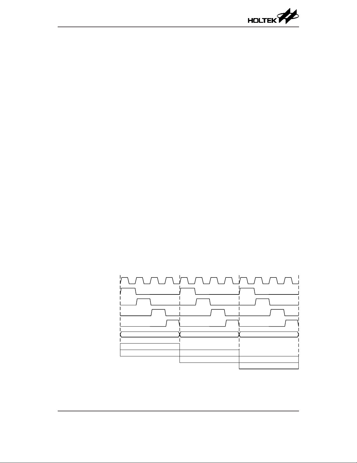
Clocking and Pipelining
The main system clock, derived from either a HIRC or LIRC oscillator is subdivided into four
internally generated non-overlapping clocks, T1~T4. The Program Counter is incremented at the
beginning of the T1 clock during which time a new instruction is fetched. The remaining T2~T4
clocks carry out the decoding and execution functions. In this way, one T1~T4 clock cycle forms
one instruction cycle. Although the fetching and execution of instructions takes place in consecutive
instruction cycles, the pipelining structure of the microcontroller ensures that instructions are
effectively executed in one instruction cycle. The exception to this are instructions where the
contents of the Program Counter are changed, such as subroutine calls or jumps, in which case the
instruction will take one more instruction cycle to execute.
For instructions involving branches, such as jump or call instructions, two machine cycles are
required to complete instruction execution. An extra cycle is required as the program takes one
cycle to rst obtain the actual jump or call address and then another cycle to actually execute the
branch. The requirement for this extra cycle should be taken into account by programmers in timing
sensitive applications.
f
(System Clock)
Phase Clock T1
Phase Clock T2
Phase Clock T3
Phase Clock T4
SYS
Pipelining
PC PC+1 PC+2
Fetch Inst. (PC)
Execute Inst. (PC-1) Fetch Inst. (PC+1)
Execute Inst. (PC)
System Clocking and Pipelining
Fetch Inst. (PC+2)
Execute Inst. (PC+1)
Page 22

HT45F6530
AC Voltage Regulator Flash MCU
1 MOV A,[12H]
2 CALL DELAY
3 CPL [12H]
4 :
5 :
6 DELAY: NOP
Program Counter
During program execution, the Program Counter is used to keep track of the address of the
next instruction to be executed. It is automatically incremented by one each time an instruction
is executed except for instructions, such as “JMP” or “CALL” that demand a jump to a non-
consecutive Program Memory address. Only the lower 8 bits, known as the Program Counter Low
Register, are directly addressable by the application program.
When executing instructions requiring jumps to non-consecutive addresses such as a jump
instruction, a subroutine call, interrupt or reset, etc., the microcontroller manages program control
by loading the required address into the Program Counter. For conditional skip instructions, once
the condition has been met, the next instruction, which has already been fetched during the present
instruction execution, is discarded and a dummy cycle takes its place while the correct instruction is
obtained.
Fetch Inst. 1
High Byte Low Byte (PCL)
PC10~PC8 PCL7~PCL0
Execute Inst. 1
Fetch Inst. 2 Execute Inst. 2
Fetch Inst. 3 Flush Pipeline
Instruction Fetching
Program Counter
Program Counter
Fetch Inst. 6 Execute Inst. 6
Fetch Inst. 7
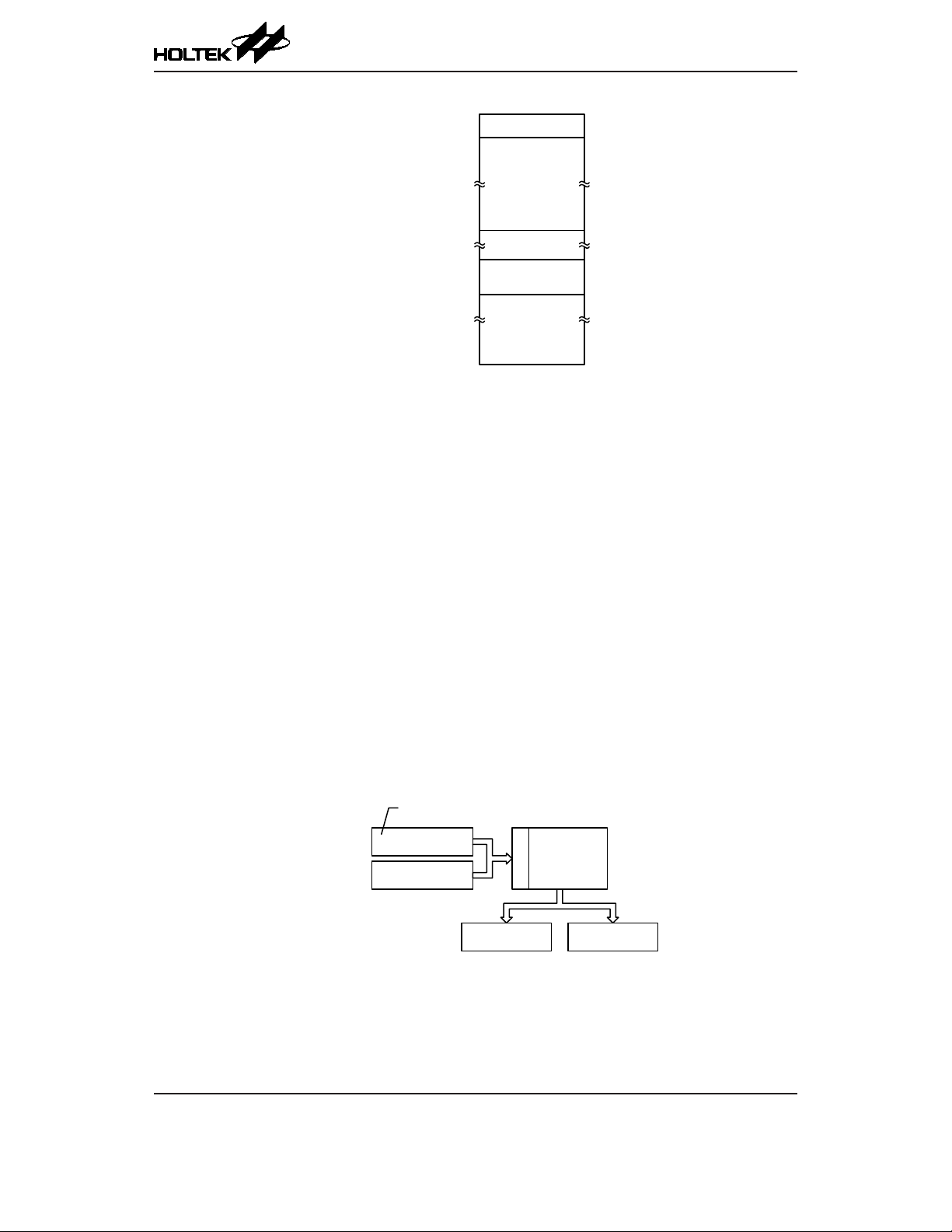
Stack
The lower byte of the Program Counter, known as the Program Counter Low register or PCL, is
available for program control and is a readable and writeable register. By transferring data directly
into this register, a short program jump can be executed directly; however, as only this low byte
is available for manipulation, the jumps are limited to the present page of memory that is 256
locations. When such program jumps are executed it should also be noted that a dummy cycle
will be inserted. Manipulating the PCL register may cause program branching, so an extra cycle is
needed to pre-fetch.
This is a special part of the memory which is used to save the contents of the Program Counter
only. The stack is organized into 4 levels and neither part of the data nor part of the program space,
and is neither readable nor writeable. The activated level is indexed by the Stack Pointer, and is
neither readable nor writeable. At a subroutine call or interrupt acknowledge signal, the contents of
the Program Counter are pushed onto the stack. At the end of a subroutine or an interrupt routine,
signaled by a return instruction, RET or RETI, the Program Counter is restored to its previous value
from the stack. After a device reset, the Stack Pointer will point to the top of the stack.
If the stack is full and an enabled interrupt takes place, the interrupt request ag will be recorded but
the acknowledge signal will be inhibited. When the Stack Pointer is decremented, by RET or RETI,
the interrupt will be serviced. This feature prevents stack overow allowing the programmer to use
the structure more easily. However, when the stack is full, a CALL subroutine instruction can still
be executed which will result in a stack overow. Precautions should be taken to avoid such cases
which might cause unpredictable program branching.
If the stack is overow, the rst Program Counter save in the stack will be lost.
Rev. 1.00 22 August 29, 2018 Rev. 1.00 23 August 29, 2018
Page 23

HT45F6530
AC Voltage Regulator Flash MCU
Program Counter
Top of Stack
Stack
Pointer
Bottom of Stack
Arithmetic and Logic Unit – ALU
The arithmetic-logic unit or ALU is a critical area of the microcontroller that carries out arithmetic
and logic operations of the instruction set. Connected to the main microcontroller data bus, the ALU
receives related instruction codes and performs the required arithmetic or logical operations after
which the result will be placed in the specied register. As these ALU calculation or operations may
result in carry, borrow or other status changes, the status register will be correspondingly updated to
reect these changes. The ALU supports the following functions:
• Arithmetic operations:
ADD, ADDM, ADC, ADCM, SUB, SUBM, SBC, SBCM, DAA
• Logic operations:
AND, OR, XOR, ANDM, ORM, XORM, CPL, CPLA
• Rotation:
RRA, RR, RRCA, RRC, RLA, RL, RLCA, RLC
• Increment and Decrement:
INCA, INC, DECA, DEC
• Branch decision:
JMP, SZ, SZA, SNZ, SIZ, SDZ, SIZA, SDZA, CALL, RET, RETI
Stack Level 1
Stack Level 2
Stack Level 3
Stack Level 4
Program Memory
Flash Program Memory
The Program Memory is the location where the user code or program is stored. For the device the
Program Memory is Flash type, which means it can be programmed and re-programmed a large
number of times, allowing the user the convenience of code modication on the same device. By
using the appropriate programming tools, the Flash device offers users the exibility to conveniently
debug and develop their applications while also offering a means of field programming and
updating.
Structure
The Program Memory has a capacity of 2K×15 bits. The Program Memory is addressed by the
Program Counter and also contains data, table information and interrupt entries. Table data, which
can be setup in any location within the Program Memory, is addressed by a separate table pointer
register.
Page 24
0000H
0004H
002CH
n00H
nFFH
HT45F6530
AC Voltage Regulator Flash MCU
Initialisation Vector
Interrupt Vectors
Look-up Table
Special Vectors
Within the Program Memory, certain locations are reserved for the reset and interrupts. The location
0000H is reserved for use by the device reset for program initialisation. After a device reset is
initiated, the program will jump to this location and begin execution.
Look-up Table
Any location within the Program Memory can be dened as a look-up table where programmers can
store xed data. To use the look-up table, the table pointer must rst be setup by placing the address
of the look up data to be retrieved in the table pointer register, TBLP. This register denes the total
address of the look-up table.
After setting up the table pointer, the table data can be retrieved from the Program Memory
using the “TABRDC [m]” or “TABRDL [m]” instructions, respectively. When the instruction is
executed, the lower order table byte from the Program Memory will be transferred to the user
dened Data Memory register [m] as specied in the instruction. The higher order table data byte
from the Program Memory will be transferred to the TBLH special register. Any unused bits in this
transferred higher order byte will be read as 0.
The accompanying diagram illustrates the addressing data ow of the look-up table.
07FFH
Program Memory Structure
Last Page or
present page
PC10~PC8
PC High Byte
TBLP Register
15 bits
Program Memory
Address
Data
15 bits
Register TBLH
High Byte Low Byte
User Selected
Register
Table Program Example
The following example shows how the table pointer and table data is dened and retrieved from the
microcontroller. This example uses raw table data located in the Program Memory which is stored
there using the ORG statement. The value at this ORG statement is “0700H” which refers to the start
Rev. 1.00 24 August 29, 2018 Rev. 1.00 25 August 29, 2018
Page 25

HT45F6530
AC Voltage Regulator Flash MCU
address of the last page within the 2K Program Memory of the microcontroller. The table pointer low
byte register is setup here to have an initial value of “06H”. This will ensure that the rst data read
from the data table will be at the Program Memory address “0706H” or 6 locations after the start of
the last page. Note that the value for the table pointer is referenced to the rst address of the present
page if the “TABRDC [m]” instruction is being used. The high byte of the table data which in this
case is equal to zero will be transferred to the TBLH register automatically when the “TABRDL [m]”
instruction is executed.
Because the TBLH register is a read-only register and cannot be restored, care should be taken
to ensure its protection if both the main routine and Interrupt Service Routine use table read
instructions. If using the table read instructions, the Interrupt Service Routines may change the
value of the TBLH and subsequently cause errors if used again by the main routine. As a rule it is
recommended that simultaneous use of the table read instructions should be avoided. However, in
situations where simultaneous use cannot be avoided, the interrupts should be disabled prior to the
execution of any main routine table-read instructions. Note that all table related instructions require
two instruction cycles to complete their operation.
Table Read Program Example
tempreg1 db ? ; temporary register #1
tempreg2 db ? ; temporary register #2
:
mov a,06h ; initialize table pointer - note that this address is referenced
mov tblp,a ; to the last page or present page
:
tabrdl tempreg1 ; transfers value in table referenced by table pointer to tempreg1
; data at program memory address “0706H” transferred to
; tempreg1 and TBLH
dec tblp ; reduce value of table pointer by one
tabrdl tempreg2 ; transfers value in table referenced by table pointer to tempreg2
; data at program memory address “0705H” transferred to
; tempreg2 and TBLH
; in this example the data “1AH” is transferred to
; tempreg1 and data “0FH” to register tempreg2
; the value “00H” will be transferred to the high byte
; register TBLH
:
org 0700h ; sets initial address of last page
dc 00Ah, 00Bh, 00Ch, 00Dh, 00Eh, 00Fh, 01Ah, 01Bh
:
In Circuit Programming – ICP
The provision of Flash type Program Memory provides the user with a means of convenient and
easy upgrades and modications to their programs on the same device.
As an additional convenience, Holtek has provided a means of programming the microcontroller in-
circuit using a 4-pin interface. This provides manufacturers with the possibility of manufacturing
their circuit boards complete with a programmed or un-programmed microcontroller, and then
programming or upgrading the program at a later stage. This enables product manufacturers to easily
keep their manufactured products supplied with the latest program releases without removal and re-
insertion of the device.
Page 26

HT45F6530
AC Voltage Regulator Flash MCU
Holtek Writer Pins MCU Programming Pins Pin Description
ICPDA PA0 Programming Serial Data/Address
ICPCK PA 2 Programming Clock
VDD VDD Power Supply
VSS VSS Ground
The Program Memory can be programmed serially in-circuit using this 4-wire interface. Data
is downloaded and uploaded serially on a single pin with an additional line for the clock.
Two additional lines are required for the power supply. The technical details regarding the in-
circuit programming of the device is beyond the scope of this document and will be supplied in
supplementary literature.
During the programming process, the user must take care of the ICPDA and ICPCK pins for data
and clock programming purposes to ensure that no other outputs are connected to these two pins.
Writer Connector
Writer_VDD
ICPDA
ICPCK
Writer_VSS
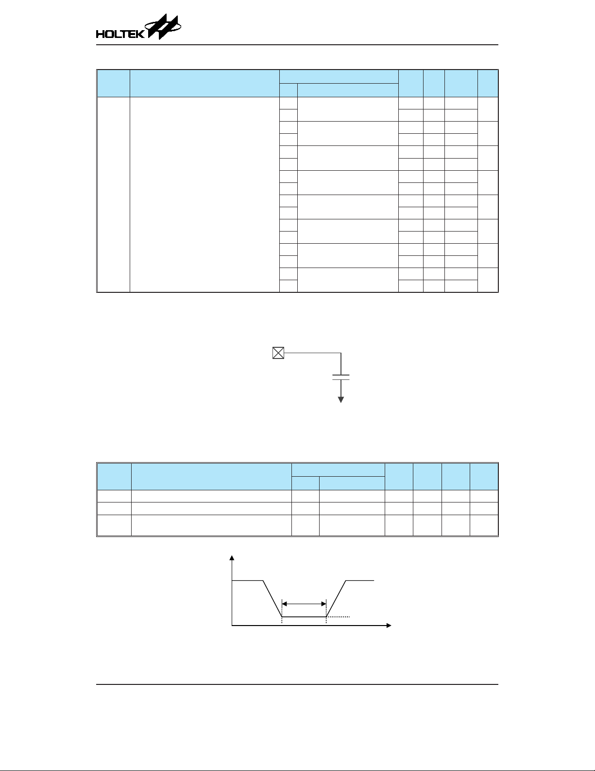
Note: * may be resistor or capacitor. The resistance of * must be greater than 1kΩ or the capacitance
of * must be less than 1nF.
On-Chip Debug Support – OCDS
There is an EV chip named HT45V6530 which is used to emulate the real MCU device named
HT45F6530. The EV chip device also provides the “On-Chip Debug” function to debug the real
MCU device during development process. The EV chip and real MCU device, HT45V6530 and
HT45F6530, are almost functional compatible except the “On-Chip Debug” function. Users can
use the EV chip device to emulate the real MCU device behaviors by connecting the OCDSDA
and OCDSCK pins to the Holtek HT-IDE development tools. The OCDSDA pin is the OCDS
Data/Address input/output pin while the OCDSCK pin is the OCDS clock input pin. When users
use the EV chip device for debugging, the corresponding pin functions shared with the OCDSDA
and OCDSCK pins in the real MCU device will have no effect in the EV chip. However, the two
OCDS pins which are pin-shared with the ICP programming pins are still used as the Flash Memory
programming pins for ICP. For more detailed OCDS information, refer to the corresponding
document named “Holtek e-Link for 8-bit MCU OCDS User’s Guide”.
Holtek e-Link Pins EV Chip OCDS Pins Pin Description
OCDSDA OCDSDA On-Chip Debug Support Data/Address input/output
OCDSCK OCDSCK On-Chip Debug Support Clock input
VDD VDD Power Supply
VSS VSS Ground
Signals
MCU Programming
Pins
VDD
PA0
PA2
VSS
* *
To other Circuit
Rev. 1.00 26 August 29, 2018 Rev. 1.00 27 August 29, 2018
Page 27

HT45F6530
AC Voltage Regulator Flash MCU
Data Memory
The Data Memory is a volatile area of 8-bit wide RAM internal memory and is the location where
temporary information is stored.
Structure
Divided into two types, the rst of these is an area of RAM, known as the Special Function Data
Memory. Here are located registers which are necessary for correct operation of the device. Many
of these registers can be read from and written to directly under program control, however, some
remain protected from user manipulation. The second area of Data Memory is known as the General
Purpose Data Memory, which is reserved for general purpose use. All locations within this area are
read and write accessible under program control.
The overall Data Memory is subdivided into two banks. The Special Purpose Data Memory registers
are accessible in Bank 0, with the exception of the EEC register at address 40H, which is only
accessible in Bank 1. Switching between the different Data Memory banks is achieved by setting the
Bank Pointer to the correct value. The start address of the Data Memory for the device is the address
00H. The address range of the Special Purpose Data Memory for the device is from 00H to 7FH
while the address range of the General Purpose Data Memory is from 80H to FFH.
Special Purpose Data Memory General Purpose Data Memory
Located Banks Capacity Bank: Address
0, 1 128×8 Bank 0: 80H~FFH
Data Memory Summary
Special Purpose
Data Memory
(Bank 0~1)
General Purpose Data Memory
(Bank 0)
General Purpose Data Memory
All microcontroller programs require an area of read/write memory where temporary data can be
stored and retrieved for use later. It is this area of RAM memory that is known as General Purpose
Data Memory. This area of Data Memory is fully accessible by the user programing for both reading
and writing operations. By using the bit operation instructions individual bits can be set or reset
under program control giving the user a large range of exibility for bit manipulation in the Data
Memory.
00H
7FH
80H
FFH
Data Memory Structure
Bank 0
40H: EEC
(Bank 1)
Page 28

Special Purpose Data Memory
This area of Data Memory is where registers, necessary for the correct operation of the
microcontroller, are stored. Most of the registers are both readable and writeable but some are
protected and are readable only, the details of which are located under the relevant Special Function
Register section. Note that for locations that are unused, any read instruction to these addresses will
return the value “00H”.
HT45F6530
AC Voltage Regulator Flash MCU
00H
01H
02H
03H
04H
05H
06H
07H
08H
09H
0AH
0BH
0CH
0DH
0EH
0FH
10H
11H
12H
13H
14H
15H
16H
17H
18H
19H
1AH
1BH
1CH
1DH
1EH
1FH
20H
21H
22H
23H
24H
25H
26H
27H
28H
29H
2AH
2BH
2CH
2DH
2EH
2FH
Bank 0 Bank 1
IAR0
MP0
IAR1
MP1
BP
ACC
PCL
TBLP
TBLH
STATUS
RSTFC
HIRCC
SCC
PA
PAC
PAPU
PAWU
WDTC
EEA
EED
SADOL
SADOH
SADC0
SADC1
SADC2
PAS0
PAS1
CTM0C0
CTM0C1
CTM0DL
CTM0DH
CTM0AL
CTM0AH
CTM1C0
: Unused, read as 00H
Special Purpose Data Memory Structure
30H
31H
32H
33H
34H
35H
36H
37H
38H
39H
3AH
3BH
3CH
3DH
3EH
3FH
41H
42H
43H
44H
45H
46H
47H
48H
49H
4AH
4BH
4CH
4DH
4EH
4FH
50H
51H
52H
53H
54H
55H
56H
57H
58H
59H
5FH
Bank 0 Bank 1
CTM1C1
CTM1DL
CTM1DH
CTM1AL
CTM1AH
PBS0
PBS1
PCS0
PCS1
PB
PBC
PBPU
PC
PCC
PCPU
EEC40H
INTEG
INTC0
INTC1
INTC2
MFI0
MFI1
DA0H
DA0L
DAC0C
CMP0C
CMP0VOS
OP0C
OP0VOS
DA1H
DA1L
DAC1C
CMP1C
CMP1VOS
OP1C
OP1VOS
TB0C
TB1C
PSCR
LVDC
Rev. 1.00 28 August 29, 2018 Rev. 1.00 29 August 29, 2018
Page 29

HT45F6530
AC Voltage Regulator Flash MCU
Special Function Register Description
Most of the Special Function Register details will be described in the relevant functional section;
however several registers require a separate description in this section.
Indirect Addressing Registers – IAR0, IAR1
The Indirect Addressing Registers, IAR0 and IAR1, although having their locations in normal RAM
register space, do not actually physically exist as normal registers. The method of indirect addressing
for RAM data manipulation uses these Indirect Addressing Registers and Memory Pointers, in
contrast to direct memory addressing, where the actual memory address is specied. Actions on the
IAR0 and IAR1 registers will result in no actual read or write operation to these registers but rather
to the memory location specied by their corresponding Memory Pointers, MP0 or MP1. Acting as a
pair, IAR0 and MP0 can together access data from Bank 0 while the IAR1 and MP1 register pair can
access data from any Data Memory bank. As the Indirect Addressing Registers are not physically
implemented, reading the Indirect Addressing Registers indirectly will return a result of “00H” and
writing to the registers indirectly will result in no operation.
Memory Pointers – MP0, MP1
Two Memory Pointers, known as MP0 and MP1 are provided. These Memory Pointers are
physically implemented in the Data Memory and can be manipulated in the same way as normal
registers providing a convenient way with which to address and track data. When any operation to
the relevant Indirect Addressing Registers is carried out, the actual address that the microcontroller
is directed to is the address specied by the related Memory Pointer. MP0, together with Indirect
Addressing Register, IAR0, are used to access data from Bank 0, while MP1 and IAR1 are used to
access data from all banks according to BP register. Direct Addressing can only be used with Bank 0,
all other Banks must be addressed indirectly using MP1 and IAR1.
The following example shows how to clear a section of four Data Memory locations already dened
as locations adres1 to adres4.
Indirect Addressing Program Example
data .section ´data´
adres1 db ?
adres2 db ?
adres3 db ?
adres4 db ?
block db ?
code .section at 0 ´code´
org 00h
start:
mov a, 04h ; setup size of block
m ov block, a
mova,offsetadres1 ;AccumulatorloadedwithrstRAMaddress
movmp0,a ;setupmemorypointerwithrstRAMaddress
loo p:
clrIAR0 ;clearthedataataddressdenedbyMP0
inc mp0 ; increment memory pointer
sdz block ; check if last memory location has been cleared
jmp loop
continue:
The important point to note here is that in the examples shown above, no reference is made to
specic Data Memory addresses.
Page 30

Bank Pointer – BP
For this device, the Data Memory is divided into two banks, Bank 0 and Bank 1. Selecting the
required Data Memory area is achieved using the Bank Pointer. Bit 0 of the Bank Pointer is used to
select Data Memory Banks 0~1.
The Data Memory is initialised to Bank 0 after a reset, except for a WDT time-out reset in the IDLE
or SLEEP Mode, in which case, the Data Memory bank remains unaffected. Directly addressing
the Data Memory will always result in Bank 0 being accessed irrespective of the value of the Bank
Pointer. Accessing data from Bank1 must be implemented using Indirect Addressing.
• BP Register
Bit 7 6 5 4 3 2 1 0
Name — — — — — — — DMBP0
R/W — — — — — — — R/W
POR — — — — — — — 0
Bit 7~1 Unimplemented, read as “0”
Bit 0 DMBP0: Select Data Memory Banks
HT45F6530
AC Voltage Regulator Flash MCU
0: Bank 0
1: Bank 1
Accumulator – ACC
The Accumulator is central to the operation of any microcontroller and is closely related with
operations carried out by the ALU. The Accumulator is the place where all intermediate results
from the ALU are stored. Without the Accumulator it would be necessary to write the result of
each calculation or logical operation such as addition, subtraction, shift, etc., to the Data Memory
resulting in higher programming and timing overheads. Data transfer operations usually involve
the temporary storage function of the Accumulator; for example, when transferring data between
one user-defined register and another, it is necessary to do this by passing the data through the
Accumulator as no direct transfer between two registers is permitted.
Program Counter Low Register – PCL
To provide additional program control functions, the low byte of the Program Counter is made
accessible to programmers by locating it within the Special Purpose area of the Data Memory. By
manipulating this register, direct jumps to other program locations are easily implemented. Loading
a value directly into this PCL register will cause a jump to the specied Program Memory location,
however, as the register is only 8-bit wide, only jumps within the current Program Memory page are
permitted. When such operations are used, note that a dummy cycle will be inserted.
Look-up Table Registers – TBLP, TBLH
These two special function registers are used to control operation of the look-up table which is
stored in the Program Memory. TBLP is the table pointer and indicates the location where the table
data is located. Its value must be setup before any table read commands are executed. Its value
can be changed, for example using the “INC” or “DEC” instructions, allowing for easy table data
pointing and reading. TBLH is the location where the high order byte of the table data is stored
after a table read data instruction has been executed. Note that the lower order table data byte is
transferred to a user dened location.
Rev. 1.00 30 August 29, 2018 Rev. 1.00 31 August 29, 2018
Page 31

HT45F6530
AC Voltage Regulator Flash MCU
Status Register – STATUS
This 8-bit register contains the zero ag (Z), carry ag (C), auxiliary carry ag (AC), overow ag
(OV), power down ag (PDF), and watchdog time-out ag (TO). These arithmetic/logical operation
and system management ags are used to record the status and operation of the microcontroller.
With the exception of the TO and PDF ags, bits in the status register can be altered by instructions
like most other registers. Any data written into the status register will not change the TO or PDF ag.
In addition, operations related to the status register may give different results due to the different
instruction operations. The TO ag can be affected only by a system power-up, a WDT time-out or
by executing the “CLR WDT” or “HALT” instruction. The PDF ag is affected only by executing
the “HALT” or “CLR WDT” instruction or during a system power-up.
The Z, OV, AC, and C ags generally reect the status of the latest operations.
• C is set if an operation results in a carry during an addition operation or if a borrow does not take
place during a subtraction operation; otherwise C is cleared. C is also affected by a rotate through
carry instruction.
• AC is set if an operation results in a carry out of the low nibbles in addition, or no borrow from
the high nibble into the low nibble in subtraction; otherwise AC is cleared.
• Z is set if the result of an arithmetic or logical operation is zero; otherwise Z is cleared.
• OV is set if an operation results in a carry into the highest-order bit but not a carry out of the
highest-order bit, or vice versa; otherwise OV is cleared.
• PDF is cleared by a system power-up or executing the “CLR WDT” instruction. PDF is set by
executing the “HALT” instruction.
• TO is cleared by a system power-up or executing the “CLR WDT” or “HALT” instruction. TO is
set by a WDT time-out.
In addition, on entering an interrupt sequence or executing a subroutine call, the status register will
not be pushed onto the stack automatically. If the contents of the status registers are important and if
the subroutine can corrupt the status register, precautions must be taken to correctly save it.
Page 32

HT45F6530
AC Voltage Regulator Flash MCU
• STATUS Register
Bit 7 6 5 4 3 2 1 0
Name — — TO PDF OV Z AC C
R/W — — R R R/W R/W R/W R/W
POR — — 0 0 x x x x
Bit 7~6 Unimplemented, read as “0”
Bit 5 TO: Watchdog Time-out ag
0: After power up or executing the “CLR WDT” or “HALT” instruction
1: A watchdog time-out occurred.
Bit 4 PDF: Power down ag
0: After power up or executing the “CLR WDT” instruction
1: By executing the “HALT” instruction
Bit 3 OV: Overow ag
0: No overow
1: An operation results in a carry into the highest-order bit but not a carry out of the
highest-order bit or vice versa.
Bit 2 Z: Zero ag
0: The result of an arithmetic or logical operation is not zero
1: The result of an arithmetic or logical operation is zero
Bit 1 AC: Auxiliary ag
0: No auxiliary carry
1: An operation results in a carry out of the low nibbles in addition, or no borrow
from the high nibble into the low nibble in subtraction
Bit 0 C: Carry ag
0: No carry-out
1: An operation results in a carry during an addition operation or if a borrow does
not take place during a subtraction operation
The “C” ag is also affected by a rotate through carry instruction.
“x”: unknown
Rev. 1.00 32 August 29, 2018 Rev. 1.00 33 August 29, 2018
Page 33
HT45F6530
AC Voltage Regulator Flash MCU
EEPROM Data Memory
This device contains an area of internal EEPROM Data Memory. EEPROM is by its nature a non-
volatile form of re-programmable memory, with data retention even when its power supply is
removed. By incorporating this kind of data memory, a whole new host of application possibilities
are made available to the designer. The availability of EEPROM storage allows information such
as product identication numbers, calibration values, specic user data, system setup data or other
product information to be stored directly within the product microcontroller. The process of reading
and writing data to the EEPROM memory has been reduced to a very trivial affair.
EEPROM Data Memory Structure
The EEPROM Data Memory capacity is 32×8 bits for the device. Unlike the Program Memory and
RAM Data Memory, the EEPROM Data Memory is not directly mapped into memory space and
is therefore not directly addressable in the same way as the other types of memory. Read and Write
operations to the EEPROM are carried out in single byte operations using an address and a data
register in Bank 0 and a single control register in Bank 1.
EEPROM Registers
Three registers control the overall operation of the internal EEPROM Data Memory. These are the
address registers, EEA, the data register, EED and a single control register, EEC. As both the EEA
and EED registers are located in Bank 0, they can be directly accessed in the same way as any other
Special Function Register. The EEC register however, being located in Bank1, cannot be directly
addressed directly and can only be read from or written to indirectly using the MP1 Memory Pointer
and Indirect Addressing Register, IAR1. Because the EEC control register is located at address 40H
in Bank 1, the MP1 Memory Pointer must rst be set to the value 40H and the Bank Pointer register,
BP, set to the value, 01H, before any operations on the EEC register are executed.
Register
Name
EEA — — — EEA4 EEA3 EEA2 EEA1 EEA0
EED D7 D6 D5 D4 D3 D2 D1 D0
EEC — — — — WREN WR RDEN RD
7 6 5 4 3 2 1 0
Bit
EEPROM Register List
• EEA Register
Bit 7 6 5 4 3 2 1 0
Name — — — EEA4 EEA3 EEA2 EEA1 EEA0
R/W — — — R/W R/W R/W R/W R/W
POR — — — 0 0 0 0 0
Bit 7~5 Unimplemented, read as “0”
Bit 4~0 EEA4~EEA0: Data EEPROM address bit 4~bit 0
• EED Register
Bit 7 6 5 4 3 2 1 0
Name D7 D6 D5 D4 D3 D2 D1 D0
R/W R/W R/W R/W R/W R/W R/W R/W R/W
POR 0 0 0 0 0 0 0 0
Bit 7~0 D7~D0: Data EEPROM data bit 7~bit 0
Page 34

HT45F6530
AC Voltage Regulator Flash MCU
• EEC Register
Bit 7 6 5 4 3 2 1 0
Name — — — — WREN WR RDEN RD
R/W — — — — R/W R/W R/W R/W
POR — — — — 0 0 0 0
Bit 7~4 Unimplemented, read as “0”
Bit 3 WREN: Data EEPROM Write Enable
0: Disable
1: Enable
This is the Data EEPROM Write Enable Bit which must be set high before Data
EEPROM write operations are carried out. Clearing this bit to zero will inhibit Data
EEPROM write operations.
Bit 2 WR: EEPROM Write Control
0: Write cycle has nished
1: Activate a write cycle
This is the Data EEPROM Write Control Bit and when set high by the application
program will activate a write cycle. This bit will be automatically reset to zero by the
hardware after the write cycle has nished. Setting this bit high will have no effect if
the WREN has not rst been set high.
Bit 1 RDEN: Data EEPROM Read Enable
0: Disable
1: Enable
This is the Data EEPROM Read Enable Bit which must be set high before Data
EEPROM read operations are carried out. Clearing this bit to zero will inhibit Data
EEPROM read operations.
Bit 0 RD: EEPROM Read Control
0: Read cycle has nished
1: Activate a read cycle
This is the Data EEPROM Read Control Bit and when set high by the application
program will activate a read cycle. This bit will be automatically reset to zero by the
hardware after the read cycle has nished. Setting this bit high will have no effect if
the RDEN has not rst been set high.
Note: 1. The WREN, WR, RDEN and RD cannot be set high at the same time in one instruction. The
WR and RD cannot be set high at the same time.
2. Ensure that the f
3. Ensure that the write operation is totally complete before changing the EEC register content.
clock is stable before executing the write operation.
SUB
Reading Data from the EEPROM
To read data from the EEPROM, the read enable bit, RDEN, in the EEC register must rst be set
high to enable the read function. The EEPROM address of the data to be read must then be placed
in the EEA register. If the RD bit in the EEC register is now set high, a read cycle will be initiated.
Setting the RD bit high will not initiate a read operation if the RDEN bit has not been set. When
the read cycle terminates, the RD bit will be automatically cleared to zero, after which the data can
be read from the EED register. The data will remain in the EED register until another read or write
operation is executed. The application program can poll the RD bit to determine when the data is
valid for reading.
Rev. 1.00 34 August 29, 2018 Rev. 1.00 35 August 29, 2018
Page 35

HT45F6530
AC Voltage Regulator Flash MCU
Writing Data to the EEPROM
To write data to the EEPROM, the EEPROM address of the data to be written must rst be placed
in the EEA register and the data placed in the EED register. Then the write enable bit, WREN, in
the EEC register must rst be set high to enable the write function. After this, the WR bit in the
EEC register must be immediately set high to initiate a write cycle. These two instructions must be
executed in two consecutive instructions. The global interrupt bit EMI should also rst be cleared
before implementing any write operations, and then set again after the write cycle has started. Note
that setting the WR bit high will not initiate a write cycle if the WREN bit has not been set. As
the EEPROM write cycle is controlled using an internal timer whose operation is asynchronous to
microcontroller system clock, a certain time will elapse before the data will have been written into
the EEPROM. Detecting when the write cycle has nished can be implemented either by polling the
WR bit in the EEC register or by using the EEPROM interrupt. When the write cycle terminates,
the WR bit will be automatically cleared to zero by the microcontroller, informing the user that the
data has been written to the EEPROM. The application program can therefore poll the WR bit to
determine when the write cycle has ended.
Write Protection
Protection against inadvertent write operation is provided in several ways. After the device is
powered-on the Write Enable bit in the control register will be cleared preventing any write
operations. Also at power-on the Bank Pointer, BP, will be reset to zero, which means that Data
Memory Bank 0 will be selected. As the EEPROM control register is located in Bank 1, this adds a
further measure of protection against spurious write operations. During normal program operation,
ensuring that the Write Enable bit in the control register is cleared will safeguard against incorrect
write operations.
EEPROM Interrupt
The EEPROM write interrupt is generated when an EEPROM write cycle has ended. The EEPROM
interrupt must first be enabled by setting the DEE bit in the relevant interrupt register. When an
EEPROM write cycle ends, the DEF request ag will be set. If the EEPROM interrupt is enabled
and the stack is not full, a jump to the associated EEPROM Interrupt vector will take place. When
the interrupt is serviced, the EEPROM interrupt request ag, DEF, will be automatically reset and
the EMI bit will be automatically cleared to disable other interrupts. More details can be obtained in
the Interrupt section.
Programming Considerations
Care must be taken that data is not inadvertently written to the EEPROM. Protection can be
enhanced by ensuring that the Write Enable bit is normally cleared to zero when not writing. Also
the Bank Pointer could be normally cleared to zero as this would inhibit access to Bank 1 where the
EEPROM control register exists. Although certainly not necessary, consideration might be given
in the application program to the checking of the validity of new write data by a simple read back
process.
When writing data the WR bit must be set high immediately after the WREN bit has been set high,
to ensure the write cycle executes correctly. The global interrupt bit EMI should also be cleared
before a write cycle is executed and then re-enabled after the write cycle starts. Note that the device
should not enter the IDLE or SLEEP mode until the EEPROM read or write operation is totally
complete. Otherwise, the EEPROM read or write operation will fail.
Page 36

HT45F6530
AC Voltage Regulator Flash MCU
Programming Examples
Reading data from the EEPROM – polling method
MOVA,EEPROM_ADRES ;userdenedaddress
MOVEEA,A
MOVA,040H ;setupmemorypointerMP1
MOVMP1,A ;MP1pointstoEECregister
MOVA,01H ;setupBankPointer
MOVBP,A
SETIAR1.1 ;setRDENbit,enablereadoperations
SETIAR1.0 ;startReadCycle-setRDbit
BACK:
SZIAR1.0 ;checkforreadcycleend
JMPBACK
CLRIAR1 ;disableEEPROMreadifnomorereadoperationsarerequired
CLRBP
MOVA,EED ;movereaddatatoregister
MOVREAD_DATA,A
Note: For each read operation, the address register should be re-specied followed by setting the RD
bit high to activate a read cycle even if the target address is consecutive.
Writing Data to the EEPROM – polling method
MOVA,EEPROM_ADRES ;userdenedaddress
MOVEEA,A
MOVA,EEPROM_DATA ;userdeneddata
MOVEED,A
MOVA,040H ;setupmemorypointerMP1
MOVMP1,A ;MP1pointstoEECregister
MOVA,01H ;setupBankPointer
MOVBP,A
CLREMI
SETIAR1.3 ;setWRENbit,enablewriteoperations
SETIAR1.2 ;startWriteCycle-setWRbit
;–executedimmediatelyaftersetWRENbit
SETEMI
BACK:
SZIAR1.2 ;checkforwritecycleend
JMPBACK
CLRIAR1;disableEEPROMwrite
CLRBP
Rev. 1.00 36 August 29, 2018 Rev. 1.00 37 August 29, 2018
Page 37
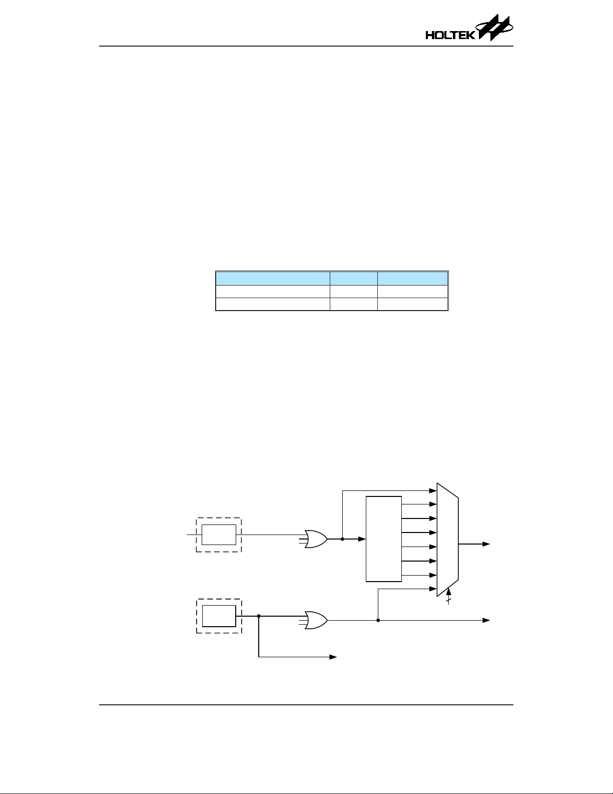
HT45F6530
AC Voltage Regulator Flash MCU
Oscillators
Various oscillator options offer the user a wide range of functions according to their various
application requirements. The flexible features of the oscillator functions ensure that the best
optimisation can be achieved in terms of speed and power saving. Oscillator selections and operation
are selected through registers.
Oscillator Overview
In addition to being the source of the main system clock the oscillators also provide clock sources
for the Watchdog Timer and Time Base Interrupts. Two fully integrated internal oscillators, requiring
no external components, are provided to form a wide range of both fast and slow system oscillators.
The high frequency oscillator provides higher performance but carries with it the disadvantage of
higher power requirements, while the opposite is of course true for the lower frequency oscillator.
With the capability of dynamically switching between fast and slow system clock, the device has the
exibility to optimise the performance/power ratio, a feature especially important in power sensitive
portable applications.
Type Name Frequency
Internal High Speed RC HIRC 8MHz
Internal Low Speed RC LIRC 32kHz
Oscillator Types
System Clock Congurations
There are two methods of generating the system clock, one high speed oscillator and one low speed
oscillator. The high speed oscillator is the internal 8MHz RC oscillator, known as the HIRC. The
low speed oscillator is the internal 32kHz RC oscillator, known as the LIRC. Selecting whether the
low or high speed oscillator is used as the system oscillator is implemented using the CKS2~CKS0
bits in the SCC register and as the system clock can be dynamically selected.
The frequency of the slow speed or high speed system clock is also determined using CKS2~CKS0
bits in the SCC register. Note that two oscillator selections must be made namely one high speed and
one low speed system oscillators. It is not possible to choose a no-oscillator selection for either the
high or low speed oscillator.
High Speed
Oscillator
HIRCHIRCEN
Low Speed
Oscillator
LIRC
f
LIRC
IDLE0
SLEEP
IDLE2
SLEEP
f
H
/2
f
H
/4
f
H
f
/8
H
Prescaler
f
SUB
/16
f
H
/32
f
H
f
/64
H
CKS2~CKS0
f
SYS
f
SUB
f
LIRC
System Clock Congurations
Page 38

Internal High Speed RC Oscillator – HIRC
The internal RC oscillator is a fully integrated system oscillator requiring no external components.
The internal RC oscillator has a fixed frequency of 8MHz. Device trimming during the
manufacturing process and the inclusion of internal frequency compensation circuits are used to
ensure that the inuence of the power supply voltage, temperature and process variations on the
oscillation frequency are also minimised.
Internal 32kHz Oscillator – LIRC
The Internal 32kHz System Oscillator is the low frequency oscillator. It is a fully integrated
RC oscillator with a typical frequency of 32kHz, requiring no external components for its
implementation. Device trimming during the manufacturing process and the inclusion of internal
frequency compensation circuits are used to ensure that the inuence of the power supply voltage,
temperature and process variations on the oscillation frequency are minimised.
Operating Modes and System Clocks
Present day applications require that their microcontrollers have high performance but often still
demand that they consume as little power as possible, conicting requirements that are especially
true in battery powered portable applications. The fast clocks required for high performance will
by their nature increase current consumption and of course vice-versa, lower speed clocks reduce
current consumption. As Holtek has provided this device with both high and low speed clock
sources and the means to switch between them dynamically, the user can optimise the operation of
their microcontroller to achieve the best performance/power ratio.
HT45F6530
AC Voltage Regulator Flash MCU
System Clocks
The device has many different clock sources for both the CPU and peripheral function operation. By
providing the user with a wide range of clock options using register programming, a clock system
can be congured to obtain maximum application performance.
The main system clock, can come from either a high frequency fH or low frequency f
and is selected using the CKS2~CKS0 bits in the SCC register. The high speed system clock can
be sourced from the HIRC oscillator. The low speed system clock source can be sourced from the
LIRC oscillator. The other choice, which is a divided version of the high speed system oscillator has
a range of fH/2~fH/64.
source,
SUB
Rev. 1.00 38 August 29, 2018 Rev. 1.00 39 August 29, 2018
Page 39

HT45F6530
AC Voltage Regulator Flash MCU
High Speed
Oscillator
HIRCHIRCEN
Low Speed
Oscillator
LIRC
f
LIRC
IDLE0
SLEEP
IDLE2
SLEEP
f
LIRC
f
SUB
Prescaler
WDT
f
SYS
f
f
f
f
f
SYS
/4
f
SUB
H
/2
H
/4
H
/8
H
f
/16
H
/32
f
H
f
/64
H
CLKSEL[1:0]
CKS2~CKS0
f
PSC
f
SYS
f
SUB
Prescaler
TB0[2:0]TB1[2:0]
Time Base 0
Time Base 1
Device Clock Congurations
Note: When the system clock source f
is switched to f
SYS
from fH, the high speed oscillator can be stopped to
SUB
conserve the power or continue to oscillate to provide the clock source, fH~fH/64, for peripheral circuit to
use, which is determined by conguring the corresponding high speed oscillator enable control bit.
System Operation Modes
There are six different modes of operation for the microcontroller, each one with its own
special characteristics and which can be chosen according to the specific performance and
power requirements of the application. There are two modes allowing normal operation of the
microcontroller, the FAST Mode and SLOW Mode. The remaining four modes, the SLEEP, IDLE0,
IDLE1 and IDLE2 Mode are used when the microcontroller CPU is switched off to conserve power.
Operation
Mode
CPU
FHIDEN FSIDEN CKS2~CKS0
FAST On x x 000~110 fH~fH/64 On On On
SLOW On x x 111 f
IDLE0 Off 0 1
IDLE1 Off 1 1 xxx On On On On
IDLE2 Off 1 0
SLEEP Off 0 0 xxx Off Off Off On/Off
Note: 1. The fH clock will be switched on or off by configuring the corresponding oscillator enable bit in the
SLOW mode.
2. The f
clock can be switched on or off which is controlled by the WDT function being enabled or
LIRC
disabled in the SLEEP mode.
Register Setting
f
SYS
SUB
000~110 Off
111 On
000~110 On
111 Off
f
H
On/Off
(1)
f
SUB
On On
Off On On
On Off On
“x”: Don’t care
f
LIRC
(2)
Page 40

HT45F6530
AC Voltage Regulator Flash MCU
FAST Mode
As the name suggests this is one of the main operating modes where the microcontroller has all of
its functions operational and where the system clock is provided by the high speed oscillator. This
mode operates allowing the microcontroller to operate normally with a clock source will come from
the high speed oscillator HIRC. The high speed oscillator will however rst be divided by a ratio
ranging from 1 to 64, the actual ratio being selected by the CKS2~CKS0 bits in the SCC register.
Although a high speed oscillator is used, running the microcontroller at a divided clock ratio reduces
the operating current.
SLOW Mode
This is also a mode where the microcontroller operates normally although now with a slower speed
clock source. The clock source used will be from f
oscillator. Running the microcontroller in this mode allows it to run with much lower operating
currents.
SLEEP Mode
The SLEEP Mode is entered when an HALT instruction is executed and when the FHIDEN and
FSIDEN bit are low. In the SLEEP mode the CPU will be stopped. However the f
still continue to operate if the WDT function is enabled, the f
Watchdog Timer function is disabled.
SUB
. The f
clock is derived from the LIRC
SUB
LIRC
clock will be stopped too, if the
LIRC
clock can
IDLE0 Mode
The IDLE0 Mode is entered when an HALT instruction is executed and when the FHIDEN bit in
the SCC register is low and the FSIDEN bit in the SCC register is high. In the IDLE0 Mode the
CPU will be switched off but the low speed oscillator will be turned on to drive some peripheral
functions.
IDLE1 Mode
The IDLE1 Mode is entered when an HALT instruction is executed and when the FHIDEN bit in the
SCC register is high and the FSIDEN bit in the SCC register is high. In the IDLE1 Mode the CPU
will be switched off but both the high and low speed oscillators will be turned on to provide a clock
source to keep some peripheral functions operational.
IDLE2 Mode
The IDLE2 Mode is entered when an HALT instruction is executed and when the FHIDEN bit in the
SCC register is high and the FSIDEN bit in the SCC register is low. In the IDLE2 Mode the CPU
will be switched off but the high speed oscillator will be turned on to provide a clock source to keep
some peripheral functions operational.
Control Register
The registers, SCC and HIRCC, are used to control the system clock and the corresponding
oscillator congurations.
Register
Name
SCC CKS2 CKS1 CKS0 — — — FHIDEN FSIDEN
HIRCC — — — — — — HIRCF HIRCEN
Bit
7 6 5 4 3 2 1 0
Rev. 1.00 40 August 29, 2018 Rev. 1.00 41 August 29, 2018
Page 41

HT45F6530
AC Voltage Regulator Flash MCU
• SCC Register
Bit 7 6 5 4 3 2 1 0
Name CKS2 CKS1 CKS0 — — — FHIDEN FSIDEN
R/W R/W R/W R/W — — — R/W R/W
POR 0 0 0 — — — 0 0
Bit 7~5 CKS2~CKS0: System clock selection
000: f
H
001: fH/2
010: fH/4
011: fH/8
100: fH/16
101: fH/32
110: fH/64
111: f
SUB
These three bits are used to select which clock is used as the system clock source. In
addition to the system clock source directly derived from fH or f
of the high speed system oscillator can also be chosen as the system clock source.
Bit 4~2 Unimplemented, read as “0”
Bit 1 FHIDEN: High frequency oscillator control when CPU is switched off
0: Disable
1: Enable
This bit is used to control whether the high speed oscillator is activated or stopped
when the CPU is switched off by executing an “HALT” instruction.
Bit 0 FSIDEN: Low frequency oscillator control when CPU is switched off
0: Disable
1: Enable
This bit is used to control whether the low speed oscillator is activated or stopped
when the CPU is switched off by executing an “HALT” instruction.
, a divided version
SUB
• HIRCC Register
Bit 7 6 5 4 3 2 1 0
Name — — — — — — HIRCF HIRCEN
R/W — — — — — — R R/W
POR — — — — — — 0 1
Bit 7~2 Unimplemented, read as “0”
Bit 1 HIRCF: HIRC oscillator stable ag
0: HIRC unstable
1: HIRC stable
This bit is used to indicate whether the HIRC oscillator is stable or not. When the
HIRCEN bit is set to 1 to enable the HIRC oscillator, the HIRCF bit will first be
cleared to 0 and then set to 1 after the HIRC oscillator is stable.
Bit 0 HIRCEN: HIRC oscillator enable control
0: Disable
1: Enable
Page 42

Operating Mode Switching
The device can switch between operating modes dynamically allowing the user to select the best
performance/power ratio for the present task in hand. In this way microcontroller operations that
do not require high performance can be executed using slower clocks thus requiring less operating
current and prolonging battery life in portable applications.
In simple terms, Mode Switching between the FAST Mode and SLOW Mode is executed using the
CKS2~CKS0 bits in the SCC register while Mode Switching from the FAST/SLOW Modes to the
SLEEP/IDLE Modes is executed via the HALT instruction. When a HALT instruction is executed,
whether the device enters the IDLE Mode or the SLEEP Mode is determined by the condition of the
FHIDEN and FSIDEN bits in the SCC register.
HT45F6530
AC Voltage Regulator Flash MCU
SLEEP
HALT instruction executed
CPU stop
FHIDEN=0
FSIDEN=0
off
f
H
off
f
SUB
FAST
f
SYS=fH~fH
fHon
/64
CPU run
f
on
SYS
f
on
SUB
HALT instruction executed
IDLE2
CPU stop
FHIDEN=1
FSIDEN=0
on
f
H
off
f
SUB
SLOW
f
SYS=fSUB
f
on
SUB
CPU run
f
on
SYS
fHon/off
HALT instruction executed
IDLE1
CPU stop
FHIDEN=1
FSIDEN=1
on
f
H
on
f
SUB
HALT instruction executed
IDLE0
CPU stop
FHIDEN=0
FSIDEN=1
off
f
H
on
f
SUB
FAST Mode to SLOW Mode Switching
When running in the FAST Mode, which uses the high speed system oscillator, and therefore
consumes more power, the system clock can switch to run in the SLOW Mode by set the
CKS2~CKS0 bits to “111” in the SCC register. This will then use the low speed system oscillator
which will consume less power. Users may decide to do this for certain operations which do not
require high performance and can subsequently reduce power consumption.
The SLOW Mode is sourced from the LIRC oscillator and therefore requires this oscillator to be
stable before full mode switching occurs.
Rev. 1.00 42 August 29, 2018 Rev. 1.00 43 August 29, 2018
Page 43

HT45F6530
AC Voltage Regulator Flash MCU
FHIDEN=1, FSIDEN=1
HALT instruction is executed
FHIDEN=1, FSIDEN=0
HALT instruction is executed
IDLE2 Mode
FAST Mode
CKS2~CKS0 = 111
SLOW Mode
FHIDEN=0, FSIDEN=0
HALT instruction is executed
SLEEP Mode
FHIDEN=0, FSIDEN=1
HALT instruction is executed
IDLE0 Mode
IDLE1 Mode
SLOW Mode to FAST Mode Switching
In SLOW mode the system clock is derived from f
FAST mode from f
, the CKS2~CKS0 bits should be set to “000”~“110” and then the system
SUB
. When system clock is switched back to the
SUB
clock will respectively be switched to fH~fH/64.
However, if fH is not used in SLOW mode and thus switched off, it will take some time to re-
oscillate and stabilise when switching to the FAST mode from the SLOW Mode. This is monitored
using the HIRCF bit in the HIRCC register. The time duration required for the high speed system
oscillator stabilization is specied in the System Start Up Time Characteristics.
SLOW Mode
CKS2~CKS0 = 000~110
FAST Mode
FHIDEN=0, FSIDEN=0
HALT instruction is executed
SLEEP Mode
FHIDEN=0, FSIDEN=1
HALT instruction is executed
IDLE0 Mode
FHIDEN=1, FSIDEN=1
HALT instruction is executed
IDLE1 Mode
FHIDEN=1, FSIDEN=0
HALT instruction is executed
IDLE2 Mode
Page 44

HT45F6530
AC Voltage Regulator Flash MCU
Entering the SLEEP Mode
There is only one way for the device to enter the SLEEP Mode and that is to execute the “HALT”
instruction in the application program with both the FHIDEN and FSIDEN bit in SCC register equal
to “0”. In this mode all the clocks and functions will be switched off except the WDT function.
When this instruction is executed under the conditions described above, the following will occur:
• The system clock will be stopped and the application program will stop at the “HALT” instruction.
• The Data Memory contents and registers will maintain their present condition.
• The I/O ports will maintain their present conditions.
• In the status register, the Power Down ag PDF will be set, and WDT timeout ag TO will be cleared.
• The WDT will be cleared and resume counting if the WDT function is enabled. If the WDT
function is disabled, the WDT will be cleared and stopped.
Entering the IDLE0 Mode
There is only one way for the device to enter the IDLE0 Mode and that is to execute the “HALT”
instruction in the application program with the FHIDEN bit in SCC register equal to “0” and the
FSIDEN bit in SCC register equal to “1”. When this instruction is executed under the conditions
described above, the following will occur:
• The fH clock will be stopped and the application program will stop at the “HALT” instruction, but
the f
clock will be on.
SUB
• The Data Memory contents and registers will maintain their present condition.
• The I/O ports will maintain their present conditions.
• In the status register, the Power Down ag PDF will be set, and WDT timeout ag TO will be
cleared.
• The WDT will be cleared and resume counting if the WDT function is enabled. If the WDT
function is disabled, the WDT will be cleared and stopped.
Entering the IDLE1 Mode
There is only one way for the device to enter the IDLE0 Mode and that is to execute the “HALT”
instruction in the application program with both the FHIDEN and FSIDEN bits in the SCC register
equal to “1”. When this instruction is executed under the conditions described above, the following
will occur:
• The fH and f
clocks will be on and the application program will stop at the “HALT” instruction.
SUB
• The Data Memory contents and registers will maintain their present condition.
• The I/O ports will maintain their present conditions.
• In the status register, the Power Down ag PDF will be set, and WDT timeout ag TO will be
cleared.
• The WDT will be cleared and resume counting if the WDT function is enabled. If the WDT
function is disabled, the WDT will be cleared and stopped.
Entering the IDLE2 Mode
There is only one way for the device to enter the IDLE2 Mode and that is to execute the “HALT”
instruction in the application program with the FHIDEN bit in the SCC register equal to “1” and the
FSIDEN bit in the SCC register equal to “0”. When this instruction is executed under the conditions
described above, the following will occur:
• The fH clock will be on but the f
clock will be off and the application program will stop at the
SUB
“HALT” instruction.
Rev. 1.00 44 August 29, 2018 Rev. 1.00 45 August 29, 2018
Page 45

HT45F6530
AC Voltage Regulator Flash MCU
• The Data Memory contents and registers will maintain their present condition.
• The I/O ports will maintain their present conditions.
• In the status register, the Power Down ag PDF will be set, and WDT timeout ag TO will be
cleared.
• The WDT will be cleared and resume counting if the WDT function is enabled. If the WDT
function is disabled, the WDT will be cleared and stopped.
Standby Current Considerations
As the main reason for entering the SLEEP or IDLE Mode is to keep the current consumption of the
device to as low a value as possible, perhaps only in the order of several micro-amps except in the
IDLE1 and IDLE2 Mode, there are other considerations which must also be taken into account by
the circuit designer if the power consumption is to be minimised. Special attention must be made
to the I/O pins on the device. All high-impedance input pins must be connected to either a xed
high or low level as any oating input pins could create internal oscillations and result in increased
current consumption. This also applies to the device which has different package types, as there may
be unbonded pins. These must either be setup as outputs or if setup as inputs must have pull-high
resistors connected.
Care must also be taken with the loads, which are connected to I/O pins, which are setup as outputs.
These should be placed in a condition in which minimum current is drawn or connected only to
external circuits that do not draw current, such as other CMOS inputs. Also note that additional
standby current will also be required if the LIRC oscillator has enabled.
In the IDLE1 and IDLE2 Mode the high speed oscillator is on, if the peripheral function clock
source is derived from the high speed oscillator, the additional standby current will also be perhaps
in the order of several hundred micro-amps.
Wake-up
To minimise power consumption the device can enter the SLEEP or any IDLE Mode, where the
CPU will be switched off. However, when the device is woken up again, it will take a considerable
time for the original system oscillator to restart, stabilise and allow normal operation to resume.
After the system enters the SLEEP or IDLE Mode, it can be woken up from one of various sources
listed as follows:
• An external falling edge on Port A
• A system interrupt
• A WDT overow
When the device executes the “HALT” instruction, the PDF ag will be set to 1. The PDF ag will
be cleared to 0 if the device experiences a system power-up or executes the clear Watchdog Timer
instruction. If the system is woken up by a WDT overow, a Watchdog Timer reset will be initiated
and the TO ag will be set to 1. The TO ag is set if a WDT time-out occurs and causes a wake-up
that only resets the Program Counter and Stack Pointer, other ags remain in their original status.
Each pin on Port A can be setup using the PAWU register to permit a negative transition on the
pin to wake-up the system. When a pin wake-up occurs, the program will resume execution at the
instruction following the “HALT” instruction. If the system is woken up by an interrupt, then two
possible situations may occur. The first is where the related interrupt is disabled or the interrupt
is enabled but the stack is full, in which case the program will resume execution at the instruction
following the “HALT” instruction. In this situation, the interrupt which woke-up the device will not
be immediately serviced, but will rather be serviced later when the related interrupt is nally enabled
Page 46

or when a stack level becomes free. The other situation is where the related interrupt is enabled and
the stack is not full, in which case the regular interrupt response takes place. If an interrupt request
flag is set high before entering the SLEEP or IDLE Mode, the wake-up function of the related
interrupt will be disabled.
Watchdog Timer
The Watchdog Timer is provided to prevent program malfunctions or sequences from jumping to
unknown locations, due to certain uncontrollable external events such as electrical noise.
Watchdog Timer Clock Source
The Watchdog Timer clock source is provided by the internal clock, f
the LIRC oscillator. The LIRC internal oscillator has an approximate frequency of 32kHz and this
specied internal clock period can vary with VDD, temperature and process variations. The Watchdog
Timer source clock is then subdivided by a ratio of 28 to 215 to give longer timeouts, the actual value
being chosen using the WS2~WS0 bits in the WDTC register.
Watchdog Timer Control Register
A single register, WDTC, controls the required time-out period as well as the enable/disable and
reset MCU operation.
HT45F6530
AC Voltage Regulator Flash MCU
which is sourced from
LIRC
• WDTC Register
Bit 7 6 5 4 3 2 1 0
Name WE4 WE3 WE2 WE1 WE0 WS2 WS1 WS0
R/W R/W R/W R/W R/W R/W R/W R/W R/W
POR 0 1 0 1 0 0 1 1
Bit 7~3 WE4~WE0: WDT function control
10101: Disable
01010: Enable
Other values: Reset MCU
When these bits are changed to any other values due to environmental noise the
microcontroller will be reset; this reset operation will be activated after a delay time,
t
, and the WRF bit in the RSTFC register will be set high.
SRESET
Bit 2~0 WS2~WS0: WDT time-out period selection
000: 28/f
001: 29/f
010: 210/f
011: 211/f
100: 212/f
101: 213/f
110: 214/f
111: 215/f
LIRC
LIRC
LIRC
LIRC
LIRC
LIRC
LIRC
LIRC
These three bits determine the division ratio of the Watchdog Timer source clock,
which in turn determines the time-out period.
Rev. 1.00 46 August 29, 2018 Rev. 1.00 47 August 29, 2018
Page 47

HT45F6530
AC Voltage Regulator Flash MCU
• RSTFC Register
Bit 7 6 5 4 3 2 1 0
Name — — — — — LVRF — WRF
R/W — — — — — R/W — R/W
POR — — — — — x — 0
Bit 7~3 Unimplemented, read as “0”
Bit 2 LVRF: LVR function reset ag
Described elsewhere
Bit 1 Unimplemented, read as “0”
Bit 0 WRF: WDTC register software reset ag
0: Not occurred
1: Occurred
This bit is set high by the WDTC register software reset and cleared by the application
program. Note that this bit can only be cleared to 0 by the application program.
Watchdog Timer Operation
The Watchdog Timer operates by providing a device reset when its timer overows. This means
that in the application program and during normal operation the user has to strategically clear the
Watchdog Timer before it overows to prevent the Watchdog Timer from executing a reset. This is
done using the clear watchdog instruction. If the program malfunctions for whatever reason, jumps
to an unknown location, or enters an endless loop, the clear instruction will not be executed in the
correct manner, in which case the Watchdog Timer will overow and reset the device. There are ve
bits, WE4~WE0, in the WDTC register to offer the enable/disable control and reset control of the
Watchdog Timer. The WDT function will be disabled when the WE4~WE0 bits are set to a value of
10101B while the WDT function will be enabled if the WE4~WE0 bits are equal to 01010B. If the
WE4~WE0 bits are set to any other values, other than 01010B and 10101B, it will reset the device
after a delay time, t
. After power on these bits will have a value of 01010B.
SRESET
WE4~WE0 Bits WDT Function
10101B Disable
01010B Enable
Any other value Reset MCU
Watchdog Timer Enable/Disable Control
“x”: unknown
Under normal program operation, a Watchdog Timer time-out will initialise a device reset and set
the status bit TO. However, if the system is in the SLEEP or IDLE Mode, when a Watchdog Timer
time-out occurs, the TO bit in the STATUS register will be set and only the Program Counter and
Stack Pointer will be reset. Three methods can be adopted to clear the contents of the Watchdog
Timer. The rst is a WDTC register software reset, which means a certain value except 01010B and
10101B written into the WE4~WE0 bits, the second is using the Watchdog Timer software clear
instruction and the third is via a HALT instruction.
There is only one method of using software instruction to clear the Watchdog Timer. That is to use
the single “CLR WDT” instruction to clear the WDT.
The maximum time-out period is when the 215 division ratio is selected. As an example, with a
32kHz LIRC oscillator as its source clock, this will give a maximum watchdog period of around 1
second for the 215 division ratio, and a minimum timeout of 8ms for the 28 division ration.
Page 48
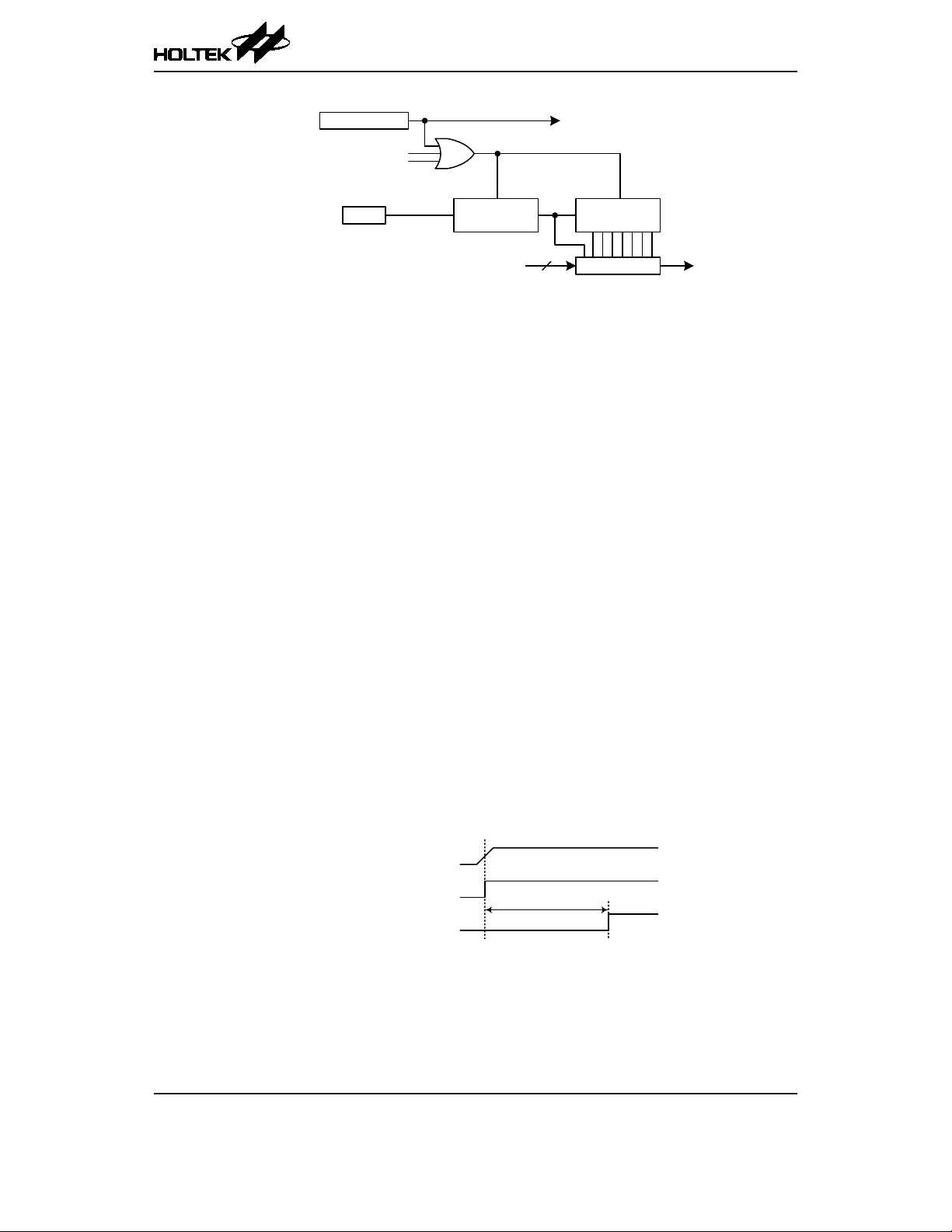
AC Voltage Regulator Flash MCU
WE4~WE0 bitsWDTC Register Reset MCU
HT45F6530
“CLR WDT” Instruction
“HALT” Instruction
Reset and Initialisation
A reset function is a fundamental part of any microcontroller ensuring that the device can be set
to some predetermined condition irrespective of outside parameters. The most important reset
condition is after power is rst applied to the microcontroller. In this case, internal circuitry will
ensure that the microcontroller, after a short delay, will be in a well-defined state and ready to
execute the rst program instruction. After this power-on reset, certain important internal registers
will be set to dened states before the program commences. One of these registers is the Program
Counter, which will be reset to zero forcing the microcontroller to begin program execution from the
lowest Program Memory address.
In addition to the power-on reset, another reset exists in the form of a Low Voltage Reset, LVR,
where a full reset is implemented in situations where the power supply voltage falls below a
certain threshold. Another type of reset is when the Watchdog Timer overflows and resets the
microcontroller. All types of reset operations result in different register conditions being setup.
CLR
f
LIRC 8-stage Divider WDT Prescaler
LIRC
f
LIRC
8
/2
8-to-1 MUXWS2~WS0
Watchdog Timer
WDT Time-out
8
/f
~215/f
(2
LIRC
LIRC
)
Reset Functions
There are several ways in which a microcontroller reset can occur, through events occurring
internally:
Power-on Reset
The most fundamental and unavoidable reset is the one that occurs after power is rst applied to
the microcontroller. As well as ensuring that the Program Memory begins execution from the rst
memory address, a power-on reset also ensures that certain other registers are preset to known
conditions. All the I/O port and port control registers will power up in a high condition ensuring that
all pins will be rst set to inputs.
Power-on Reset
SST Time-out
Note: t
RSTD
Power-on Reset Timing Chart
V
DD
t
RSTD
is power-on delay, typical time=50ms.
Rev. 1.00 48 August 29, 2018 Rev. 1.00 49 August 29, 2018
Page 49
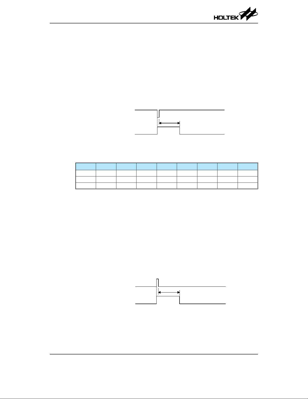
HT45F6530
AC Voltage Regulator Flash MCU
Low Voltage Reset – LVR
The microcontroller contains a low voltage reset circuit in order to monitor the supply voltage of the
device. The LVR function is always enabled during normal operation with a specic LVR voltage
V
. The actual V
LVR
range of 0.9V~V
the LVR will automatically reset the device internally and the LVRF bit in the RSTFC register will
also be set to 1. For a valid LVR signal, a low supply voltage, i.e., a voltage in the range between
0.9V~V
must exist for a time greater than that specified by t
LVR
Characteristics. If the low supply voltage state does not exceed this value, the LVR will ignore
the low supply voltage and will not perform a reset function. Note that the LVR function will be
automatically disabled when the device enters the SLEEP or IDLE mode.
value is xed at 2.1V. If the supply voltage of the device drops to within a
LVR
such as might occur when changing the battery in battery powered applications,
LVR
LVR
Internal Reset
t
RSTD
in the LVR/LVD Electrical
LVR
+ t
SST
Note: t
is power-on delay, typical time=50ms.
RSTD
Low Voltage Reset Timing Chart
• RSTFC Register
Bit 7 6 5 4 3 2 1 0
Name — — — — — LVRF — WRF
R/W — — — — — R/W — R/W
POR — — — — — x — 0
“x”: unknown
Bit 7~3 Unimplemented, read as “0”
Bit 2 LVRF: LVR function reset ag
0: Not occur
1: Occurred
This bit is set to 1 when a specic Low Voltage Reset situation condition occurs. This
bit can only be cleared to 0 by the application program.
Bit 1 Unimplemented, read as “0”
Bit 0 WRF: WDTC register software reset ag
Described elsewhere
Watchdog Time-out Reset during Normal Operation
The Watchdog time-out Reset during normal operations in the FAST or SLOW mode is the same as
the hardware low voltage reset except that the Watchdog time-out ag TO will be set to “1”.
WDT Time-out
t
+ t
RSTD
SST
Internal Reset
Note: t
WDT Time-out Reset during Normal Operation Timing Chart
is power-on delay, typical time=16.7ms.
RSTD
Page 50
AC Voltage Regulator Flash MCU
Watchdog Time-out Reset during SLEEP or IDLE Mode
The Watchdog time-out Reset during SLEEP or IDLE Mode is a little different from other kinds
of reset. Most of the conditions remain unchanged except that the Program Counter and the Stack
Pointer will be cleared to “0” and the TO ag will be set to “1”. Refer to the System Start Up Time
Characteristics for t
Reset Initial Conditions
The different types of reset described affect the reset ags in different ways. These ags, known
as PDF and TO are located in the status register and are controlled by various microcontroller
operations, such as the SLEEP or IDLE Mode function or Watchdog Timer. The reset flags are
shown in the table:
TO PDF Reset Conditions
0 0 Power-on reset
u u LVR reset during FAST or SLOW Mode operation
1 u WDT time-out reset during FAST or SLOW Mode operation
1 1 WDT time-out reset during IDLE or SLEEP Mode operation
The following table indicates the way in which the various components of the microcontroller are
affected after a power-on reset occurs.
Program Counter Reset to zero
Interrupts All interrupts will be disabled
WDT, Time Bases Clear after reset, WDT begins counting
Timer Modules Timer Modules will be turned off
Input/Output Ports I/O ports will be setup as inputs
Stack Pointer Stack Pointer will point to the top of the stack
details.
SST
WDT Time-out
Internal Reset
WDT Time-out Reset during SLEEP or IDLE Timing Chart
Item Condition after Reset
HT45F6530
t
SST
“u”: stands for unchanged
The different kinds of resets all affect the internal registers of the microcontroller in different ways.
To ensure reliable continuation of normal program execution after a reset occurs, it is important to
know what condition the microcontroller is in after a particular reset occurs. The following table
describes how each type of reset affects each of the microcontroller internal registers. Note that as
more than one package type exists the table reects the situation for the larger package type.
Register Power On Reset
IAR0 xxxx xxxx uuuu uuuu uuuu uuuu uuuu uuuu
MP0 xxxx xxxx uuuu uuuu uuuu uuuu uuuu uuuu
IAR1 xxxx xxxx uuuu uuuu uuuu uuuu uuuu uuuu
MP1 xxxx xxxx uuuu uuuu uuuu uuuu uuuu uuuu
BP ---- ---0 ---- ---0 ---- ---0 ---- ---u
ACC xxxx xxxx uuuu uuuu uuuu uuuu uuuu uuuu
PCL 0000 0000 0000 0000 0000 0000 0000 0000
TBLP xxxx xxxx uuuu uuuu uuuu uuuu uuuu uuuu
TBLH -xxx xxxx -uuu uuuu -uuu uuuu -uuu uuuu
Rev. 1.00 50 August 29, 2018 Rev. 1.00 51 August 29, 2018
LVR Reset
(Normal Operation)
WDT Time-out
(Normal Operation)
WDT Time-out
(IDLE/SLEEP)
Page 51

HT45F6530
AC Voltage Regulator Flash MCU
Register Power On Reset
STATUS --00 xxxx --uu uuuu --1u uuuu --11 uuuu
RSTFC ---- -x-0 ---- -1-u ---- -u-u ---- -u-u
HIRCC ---- --01 ---- --01 ---- --01 ---- --uu
SCC 000- --00 000- --00 000- --00 uuu- --uu
PA 1111 1111 1111 1111 1111 1111 uuuu uuuu
PAC 1111 1111 1111 1111 1111 1111 uuuu uuuu
PAPU 0000 0000 0000 0000 0000 0000 uuuu uuuu
PAWU 0000 0000 0000 0000 0000 0000 uuuu uuuu
WDTC 0101 0011 0101 0011 0101 0011 uuuu uuuu
EEA ---0 0000 ---0 0000 ---0 0000 ---u uuuu
EED 0000 0000 0000 0000 0000 0000 uuuu uuuu
SADOL xxxx ---- xxxx ---- xxxx ----
SADOH xxxx xxxx xxxx xxxx xxxx xxxx
SADC0 0000 0000 0000 0000 0000 0000 uuuu uuuu
SADC1 0000 -000 0000 -000 0000 -000 uuuu -uuu
SADC2 0--0 0000 0--0 0000 0--0 0000 u--u uuuu
PAS0 0000 0000 0000 0000 0000 0000 uuuu uuuu
PAS1 0000 0000 0000 0000 0000 0000 uuuu uuuu
CTM0C0 0000 0000 0000 0000 0000 0000 uuuu uuuu
CTM0C1 0000 0000 0000 0000 0000 0000 uuuu uuuu
CTM0DL 0000 0000 0000 0000 0000 0000 uuuu uuuu
CTM0DH ---- --00 ---- --00 ---- --00 ---- --uu
CTM0AL 0000 0000 0000 0000 0000 0000 uuuu uuuu
CTM0AH ---- --00 ---- --00 ---- --00 ---- --uu
CTM1C0 0000 0000 0000 0000 0000 0000 uuuu uuuu
CTM1C1 0000 0000 0000 0000 0000 0000 uuuu uuuu
CTM1DL 0000 0000 0000 0000 0000 0000 uuuu uuuu
CTM1DH ---- --00 ---- --00 ---- --00 ---- --uu
CTM1AL 0000 0000 0000 0000 0000 0000 uuuu uuuu
CTM1AH ---- --00 ---- --00 ---- --00 ---- --uu
PBS0 0000 0000 0000 0000 0000 0000 uuuu uuuu
PBS1 0000 0000 0000 0000 0000 0000 uuuu uuuu
PCS0 0000 0000 0000 0000 0000 0000 uuuu uuuu
PCS1 ---- 0000 ---- 0000 ---- 0000 ---- uuuu
PB 1111 1111 1111 1111 1111 1111 uuuu uuuu
PBC 1111 1111 1111 1111 1111 1111 uuuu uuuu
PBPU 0000 0000 0000 0000 0000 0000 uuuu uuuu
PC -- 11 1111 -- 11 1111 -- 11 1111 --uu uuuu
PCC --11 1111 - -11 1111 --11 1111 --uu uuuu
PCPU --00 0000 --00 0000 --00 0000 --uu uuuu
EEC ---- 0000 ---- 0000 ---- 0000 ---- uuuu
INTEG ---- 0000 ---- 0000 ---- 0000 ---- uuuu
LVR Reset
(Normal Operation)
WDT Time-out
(Normal Operation)
WDT Time-out
(IDLE/SLEEP)
uuuu ---(ADRFS=0)
uuuu uuuu
(ADRFS=1)
uuuu uuuu
(ADRFS=0)
---- uuuu
(ADRFS=1)
Page 52

HT45F6530
AC Voltage Regulator Flash MCU
Register Power On Reset
INTC0 -000 0000 -000 0000 -000 0000 -uuu uuuu
INTC1 0000 0000 0000 0000 0000 0000 uuuu uuuu
INTC2 0000 0000 0000 0000 0000 0000 uuuu uuuu
MFI0 --00 --00 --00 --00 --00 --00 --uu --uu
MFI1 --00 --00 --00 --00 --00 --00 --uu --uu
DA0H ---- 0000 ---- 0000 ---- 0000 ---- uuuu
DA0L 0000 0000 0000 0000 0000 0000 uuuu uuuu
DAC0C 00-- --00 00-- --00 00-- --00 uu-- --uu
CMP0C -000 00-- -000 00-- -000 00-- -uuu uu--
CMP0VOS -001 0000 -001 0000 -001 0000 -uuu uuuu
OP0C 00-- --00 00-- --00 00-- --00 uu-- --uu
OP0VOS 0010 0000 0010 0000 0010 0000 uuuu uuuu
DA1H ---- 0000 ---- 0000 ---- 0000 ---- uuuu
DA1L 0000 0000 0000 0000 0000 0000 uuuu uuuu
DAC1C 00-- --00 00-- --00 00-- --00 uu-- --uu
CMP1C -000 00-- -000 00-- -000 00-- -uuu uu--
CMP1VOS -001 0000 -001 0000 -001 0000 -uuu uuuu
OP1C 00-- --00 00-- --00 00-- --00 uu-- --uu
OP1VOS 0010 0000 0010 0000 0010 0000 uuuu uuuu
TB0C 0--- -000 0--- -000 0--- -000 u--- -uuu
TB1C 0--- -000 0--- -000 0--- -000 u--- -uuu
PSCR ---- --00 ---- --00 ---- --00 ---- --uu
LVDC --00 0000 --00 0000 --00 0000 --uu uuuu
LVR Reset
(Normal Operation)
WDT Time-out
(Normal Operation)
WDT Time-out
(IDLE/SLEEP)
Note: “u” stands for unchanged
“x” stands for unknown
“-” stands for unimplemented
Rev. 1.00 52 August 29, 2018 Rev. 1.00 53 August 29, 2018
Page 53
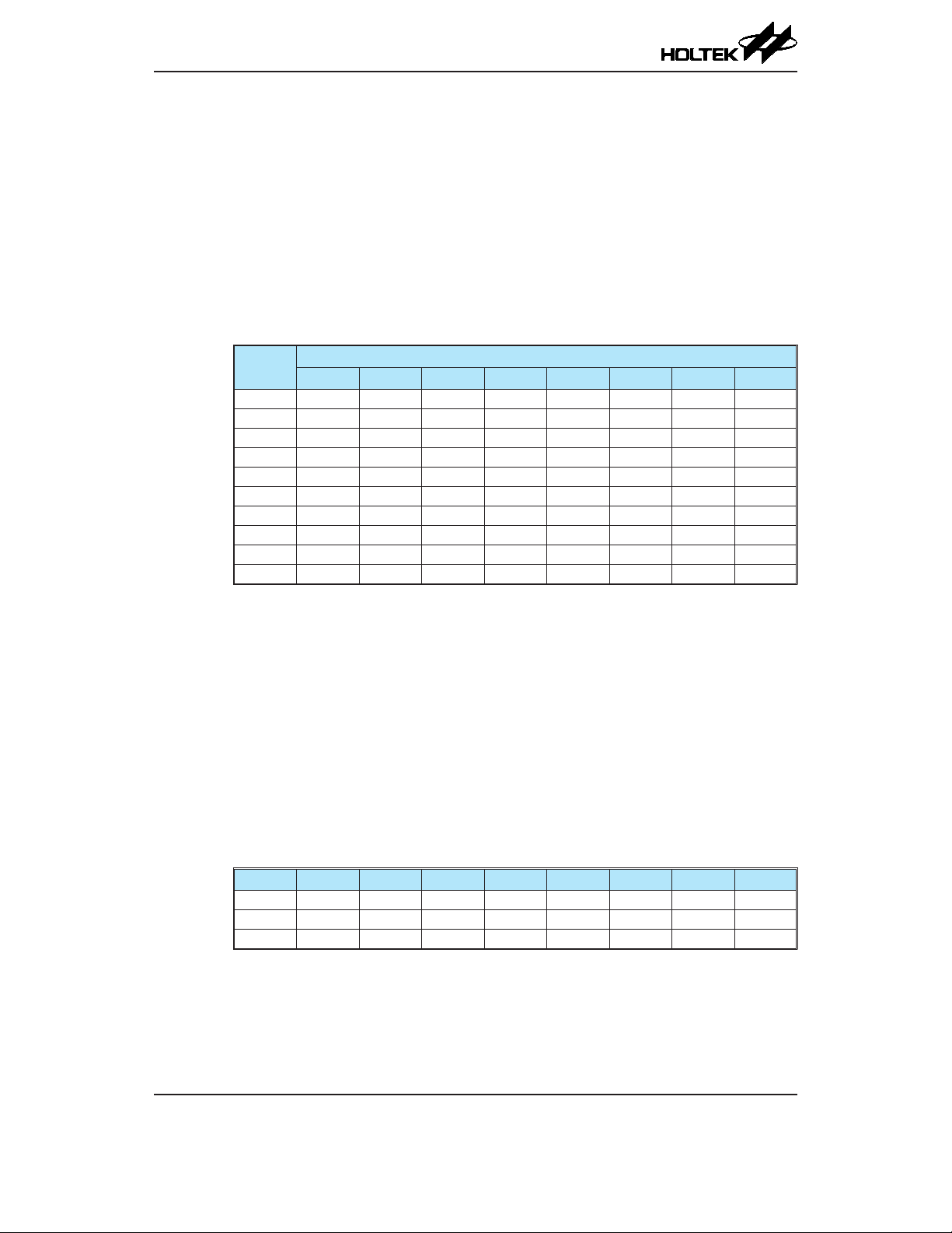
HT45F6530
AC Voltage Regulator Flash MCU
Input/Output Ports
Holtek microcontrollers offer considerable exibility on their I/O ports. With the input or output
designation of every pin fully under user program control, pull-high selections for all ports and
wake-up selections on certain pins, the user is provided with an I/O structure to meet the needs of a
wide range of application possibilities.
The device provides bidirectional input/output lines labeled with port names PA~PC. These I/O
ports are mapped to the RAM Data Memory with specic addresses as shown in the Special Purpose
Data Memory table. All of these I/O ports can be used for input and output operations. For input
operation, these ports are non-latching, which means the inputs must be ready at the T2 rising edge
of instruction “MOV A, [m]”, where m denotes the port address. For output operation, all the data is
latched and remains unchanged until the output latch is rewritten.
Register
Name
PA PA 7 PA6 PA5 PA4 PA 3 PA2 PA1 PA0
PAC PAC7 PAC6 PAC5 PAC4 PAC3 PAC2 PAC1 PAC0
PAPU PAPU7 PAPU6 PAPU5 PAPU4 PAPU3 PAPU2 PAPU1 PAPU0
PAWU PAWU7 PAWU6 PAWU5 PAWU4 PAWU3 PAWU2 PAWU1 PAWU0
PB PB7 PB6 PB5 PB4 PB3 PB2 PB1 PB0
PBC PBC7 PBC6 PBC5 PBC4 PBC3 PBC2 PBC1 PBC0
PBPU PBPU7 PBPU6 PBPU5 PBPU4 PBPU3 PBPU2 PBPU1 PBPU0
PC — — PC5 PC4 PC3 PC2 PC1 PC0
PCC — — PCC5 PCC4 PCC3 PCC2 PCC1 PCC0
PCPU — — PCPU5 PCPU4 PCPU3 PCPU2 PCPU1 PCPU0
7 6 5 4 3 2 1 0
I/O Logic Function Register List
Bit
“—”: Unimplemented, read as “0”
Pull-high Resistors
Many product applications require pull-high resistors for their switch inputs usually requiring the
use of an external resistor. To eliminate the need for these external resistors, all I/O pins, when
congured as a digital input have the capability of being connected to an internal pull-high resistor.
These pull-high resistors are selected using registers, namely PAPU~PCPU, and are implemented
using weak PMOS transistors.
Note that the pull-high resistor can be controlled by the relevant pull-high control register only when
the pin-shared functional pin is selected as a digital input or NMOS output. Otherwise, the pull-high
resistors cannot be enabled.
• PxPU Register
Bit 7 6 5 4 3 2 1 0
Name PxPU7 PxPU6 PxPU5 PxPU4 PxPU3 PxPU2 PxPU1 PxPU0
R/W R/W R/W R/W R/W R/W R/W R/W R/W
POR 0 0 0 0 0 0 0 0
PxPUn: I/O Port x Pin pull-high function control
0: Disable
1: Enable
The PxPUn bit is used to control the pin pull-high function. Here the “x” can be A, B or C.
However, the actual available bits for each I/O Port may be different.
Page 54

Port A Wake-up
The HALT instruction forces the microcontroller into the SLEEP or IDLE Mode which preserves
power, a feature that is important for battery and other low-power applications. Various methods
exist to wake-up the microcontroller, one of which is to change the logic condition on one of the Port
A pins from high to low. This function is especially suitable for applications that can be woken up
via external switches. Each pin on Port A can be selected individually to have this wake-up feature
using the PAWU register.
Note that the wake-up function can be controlled by the wake-up control registers only when the
pin-shared functional pin is selected as a general purpose input and the MCU enters the IDLE or
SLEEP mode.
• PAWU Register
Bit 7 6 5 4 3 2 1 0
Name PAWU7 PAWU6 PAWU5 PAWU4 PAWU3 PAWU2 PAWU1 PAWU0
R/W R/W R/W R/W R/W R/W R/W R/W R/W
POR 0 0 0 0 0 0 0 0
Bit 7~0 PAWU7~PAWU0: PA7~PA0 wake-up function control
HT45F6530
AC Voltage Regulator Flash MCU
0: Disable
1: Enable
I/O Port Control Registers
Each I/O port has its own control register known as PAC~PCC, to control the input/output
configuration. With this control register, each CMOS output or input can be reconfigured
dynamically under software control. Each pin of the I/O ports is directly mapped to a bit in its
associated port control register. For the I/O pin to function as an input, the corresponding bit of the
control register must be written as a “1”. This will then allow the logic state of the input pin to be
directly read by instructions. When the corresponding bit of the control register is written as a “0”,
the I/O pin will be setup as a CMOS output. If the pin is currently setup as an output, instructions
can still be used to read the output register. However, it should be noted that the program will in fact
only read the status of the output data latch and not the actual logic status of the output pin.
• PxC Register
Bit 7 6 5 4 3 2 1 0
Name PxC7 PxC6 PxC5 PxC4 PxC3 PxC2 PxC1 PxC0
R/W R/W R/W R/W R/W R/W R/W R/W R/W
POR 1 1 1 1 1 1 1 1
PxCn: I/O Port x Pin type selection
0: Output
1: Input
The PxCn bit is used to control the pin type selection. Here the “x” can be A, B or C.
However, the actual available bits for each I/O Port may be different.
Pin-shared Functions
The exibility of the microcontroller range is greatly enhanced by the use of pins that have more
than one function. Limited numbers of pins can force serious design constraints on designers but by
supplying pins with multi-functions, many of these difculties can be overcome. For these pins, the
desired function of the multi-function I/O pins is selected by a series of registers via the application
program control.
Rev. 1.00 54 August 29, 2018 Rev. 1.00 55 August 29, 2018
Page 55
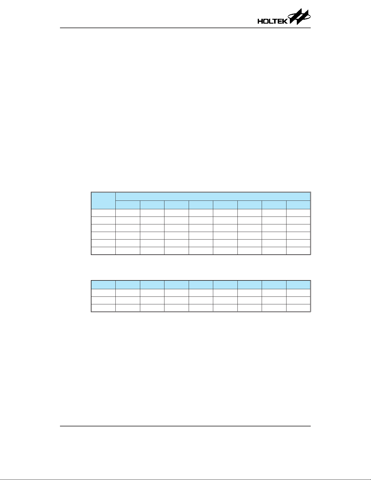
HT45F6530
AC Voltage Regulator Flash MCU
Pin-shared Function Selection Registers
The limited number of supplied pins in a package can impose restrictions on the amount of functions
a certain device can contain. However by allowing the same pins to share several different functions
and providing a means of function selection, a wide range of different functions can be incorporated
into even relatively small package sizes. The device includes Port “x” Output Function Selection
register “n”, labeled as PxSn, which can select the desired functions of the multi-function pin-shared
pins.
The most important point to note is to make sure that the desired pin-shared function is properly
selected and also deselected. For most pin-shared functions, to select the desired pin-shared function,
the pin-shared function should rst be correctly selected using the corresponding pin-shared control
register. After that the corresponding peripheral functional setting should be congured and then
the peripheral function can be enabled. However, a special point must be noted for some digital
input pins, such as INTn, xTCK, etc., which share the same pin-shared control conguration with
their corresponding general purpose I/O functions when setting the relevant pin-shared control bit
elds. To select these pin functions, in addition to the necessary pin-shared control and peripheral
functional setup aforementioned, they must also be setup as an input by setting the corresponding bit
in the I/O port control register. To correctly deselect the pin-shared function, the peripheral function
should first be disabled and then the corresponding pin-shared function control register can be
modied to select other pin-shared functions.
Register
Name
PAS0 PAS07 PAS06 PAS05 PAS04 PAS03 PAS02 PAS01 PAS00
PAS1 PAS17 PAS16 PAS15 PAS14 PAS13 PAS12 PAS 11 PAS10
PBS0 PBS07 PBS06 PBS05 PBS04 PBS03 PBS02 PBS01 PBS00
PBS1 PBS17 PBS16 PBS15 PBS14 PBS13 PBS12 PBS11 PBS10
PCS0 PCS07 PCS06 PCS05 PCS04 PCS03 PCS02 PCS01 PCS00
PCS1 — — — — PCS13 PCS12 PCS11 PCS10
7 6 5 4 3 2 1 0
Pin-shared Function Selection Register List
Bit
• PAS0 Register
Bit 7 6 5 4 3 2 1 0
Name PAS07 PAS06 PAS05 PAS04 PAS03 PAS02 PAS01 PAS00
R/W R/W R/W R/W R/W R/W R/W R/W R/W
POR 0 0 0 0 0 0 0 0
Bit 7~6 PAS07~PAS06: PA3 Pin-Shared function selection
00: PA3
01: PA3
10: VREFI
11: AN4
Bit 5~4 PAS05~PAS04: PA2 Pin-Shared function selection
00: PA2
01: CTP1
10: PA2
11: VR0EXT
Bit 3~2 PAS03~PAS02: PA1 Pin-Shared function selection
00: PA1
01: PA1
10: VREF
11: AN5
Page 56
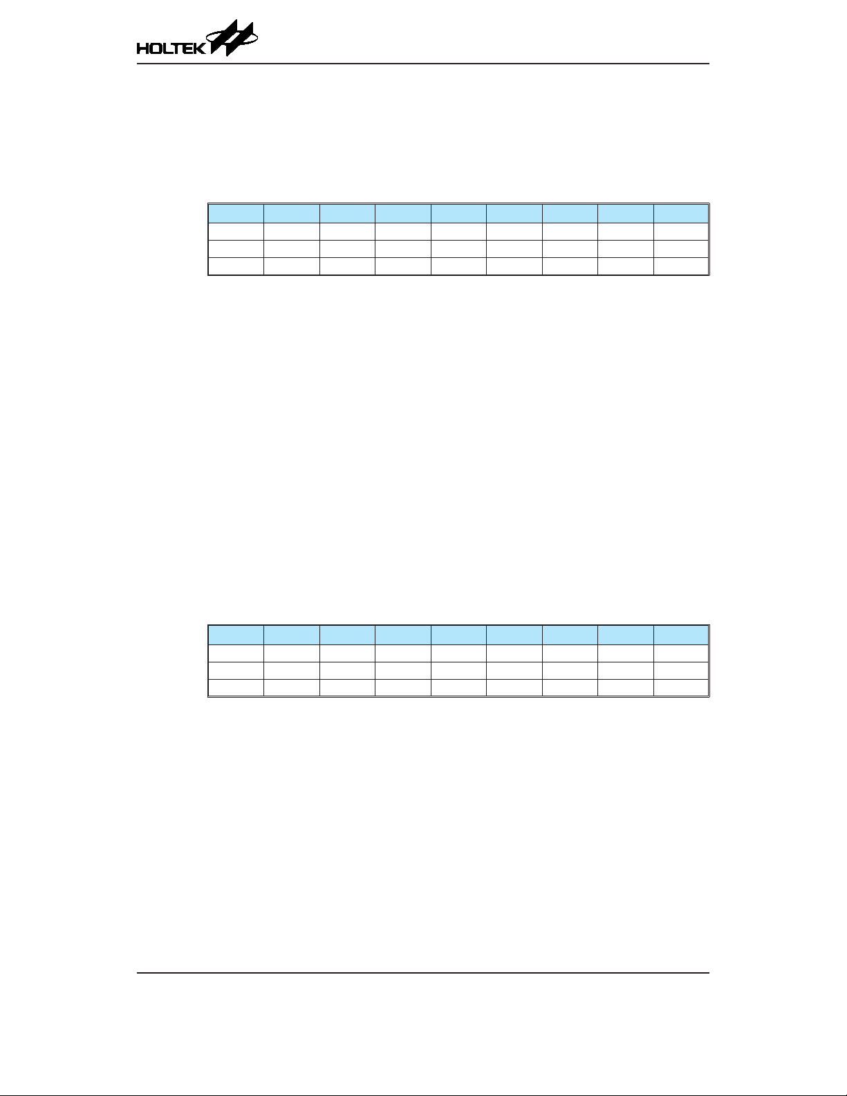
HT45F6530
AC Voltage Regulator Flash MCU
Bit 1~0 PAS01~PAS00: PA0 Pin-Shared function selection
00: PA0/INT0
01: CTP0
10: PA0/INT0
11: VR1EXT
• PAS1 Register
Bit 7 6 5 4 3 2 1 0
Name PAS17 PAS16 PAS15 PAS14 PAS13 PAS12 PAS 11 PAS10
R/W R/W R/W R/W R/W R/W R/W R/W R/W
POR 0 0 0 0 0 0 0 0
Bit 7~6 PAS17~PAS16: PA7 Pin-Shared function selection
00: PA7
01: PA7
10: PA7
11: AN0
Bit 5~4 PAS15~PAS14: PA6 Pin-Shared function selection
00: PA6
01: PA6
10: PA6
11: AN1
Bit 3~2 PAS13~PAS12: PA5 Pin-Shared function selection
00: PA5
01: PA5
10: PA5
11: AN2
Bit 1~0 PAS11~PAS10: PA4 Pin-Shared function selection
00: PA4/INT1
01: PA4/INT1
10: PA4/INT1
11: AN3
• PBS0 Register
Bit 7 6 5 4 3 2 1 0
Name PBS07 PBS06 PBS05 PBS04 PBS03 PBS02 PBS01 PBS00
R/W R/W R/W R/W R/W R/W R/W R/W R/W
POR 0 0 0 0 0 0 0 0
Bit 7~6 PBS07~PBS06: PB3 Pin-Shared function selection
00: PB3
01: PB3
10: PB3
11: CMP0P
Bit 5~4 PBS05~PBS04: PB2 Pin-Shared function selection
00: PB2
01: PB2
10: PB2
11: OPA0O
Bit 3~2 PBS03~PBS02: PB1 Pin-Shared function selection
00: PB1
01: PB1
10: PB1
11: OPA1O
Rev. 1.00 56 August 29, 2018 Rev. 1.00 57 August 29, 2018
Page 57
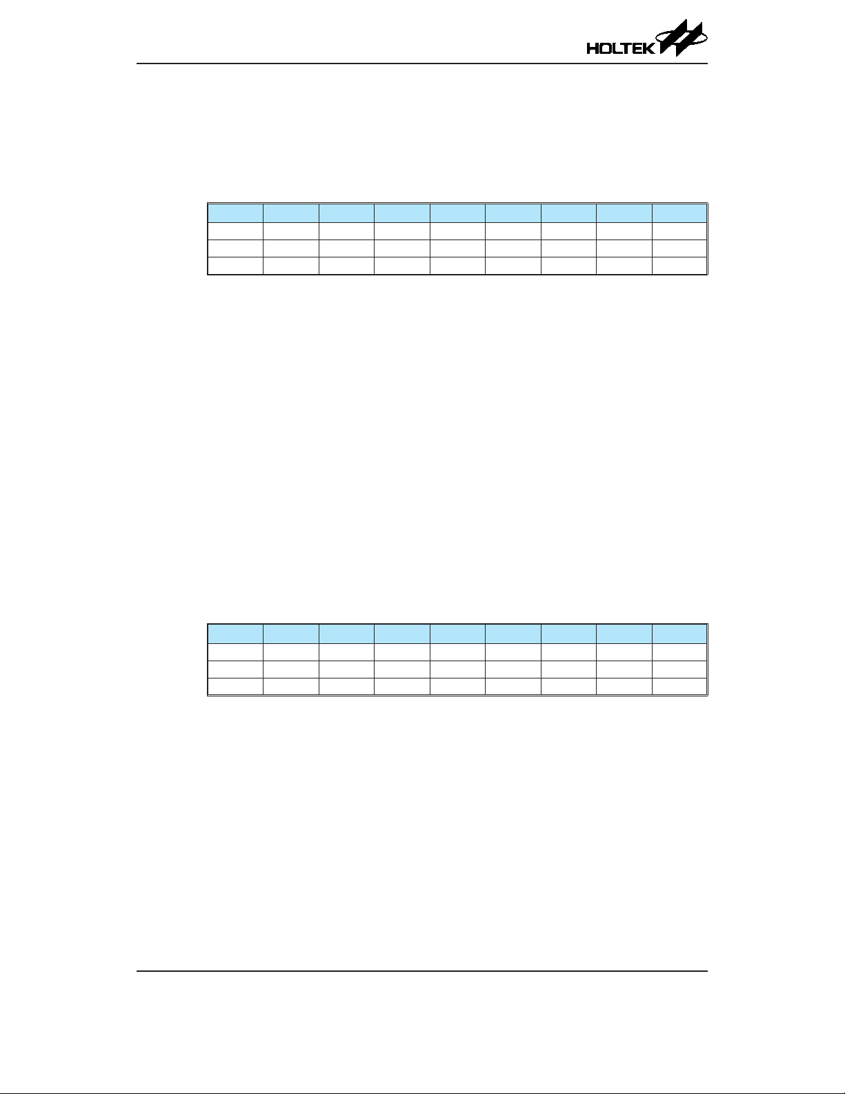
HT45F6530
AC Voltage Regulator Flash MCU
Bit 1~0 PBS01~PBS00: PB0 Pin-Shared function selection
00: PB0
01: PB0
10: PB0
11: BUF_OUT1
• PBS1 Register
Bit 7 6 5 4 3 2 1 0
Name PBS17 PBS16 PBS15 PBS14 PBS13 PBS12 PBS11 PBS10
R/W R/W R/W R/W R/W R/W R/W R/W R/W
POR 0 0 0 0 0 0 0 0
Bit 7~6 PBS17~PBS16: PB7 Pin-Shared function selection
00: PB7/CTCK1
01: PB7/CTCK1
10: PB7/CTCK1
11: CMP1O
Bit 5~4 PBS15~PBS14: PB6 Pin-Shared function selection
00: PB6
01: PB6
10: PB6
11: CMP1P
Bit 3~2 PBS13~PBS12: PB5 Pin-Shared function selection
00: PB5
01: CTP1B
10: PB5
11: CMP1N
Bit 1~0 PBS11~PBS10: PB4 Pin-Shared function selection
00: PB4
01: CTP0B
10: PB4
11: CMP0N
• PCS0 Register
Bit 7 6 5 4 3 2 1 0
Name PCS07 PCS06 PCS05 PCS04 PCS03 PCS02 PCS01 PCS00
R/W R/W R/W R/W R/W R/W R/W R/W R/W
POR 0 0 0 0 0 0 0 0
Bit 7~6 PCS07~PCS06: PC3 Pin-Shared function selection
00: PC3
01: PC3
10: PC3
11: OPA1N
Bit 5~4 PCS05~PCS04: PC2 Pin-Shared function selection
00: PC2
01: PC2
10: PC2
11: OPA1P
Bit 3~2 PCS03~PCS02: PC1 Pin-Shared function selection
00: PC1
01: PC1
10: PC1
11: BUF_OUT0
Page 58

HT45F6530
AC Voltage Regulator Flash MCU
Bit 1~0 PCS01~PCS00: PC0 Pin-Shared function selection
00: PC0/CTCK0
01: PC0/CTCK0
10: PC0/CTCK0
11: CMP0O
• PCS1 Register
Bit 7 6 5 4 3 2 1 0
Name — — — — PCS13 PCS12 PCS11 PCS10
R/W — — — — R/W R/W R/W R/W
POR — — — — 0 0 0 0
Bit 7~4 Unimplemented, read as “0”
Bit 3~2 PCS13~PCS12: PC5 Pin-Shared function selection
00: PC5
01: PC5
10: PC5
11: OPA0N
Bit 1~0 PCS11~PCS10: PC4 Pin-Shared function selection
00: PC4
01: PC4
10: PC4
11: OPA0P
I/O Pin Structures
The accompanying diagram illustrates the internal structure of the I/O logic function. As the exact
logical construction of the I/O pin will differ from this drawing, it is supplied as a guide only to
assist with the functional understanding of the I/O logic function. The wide range of pin-shared
structures does not permit all types to be shown.
Data Bus
Write Control Register
Chip Reset
Read Control Register
Write Data Register
Read Data Register
System Wake-up
Logic Function Input/Output Structure
Control Bit
D
Q
CK
Q
S
Data Bit
Q
D
Q
CK
S
Pull-high
Register
Select
M
U
X
wake-up Select
V
DD
PA only
Weak
Pull-up
I/O pin
Rev. 1.00 58 August 29, 2018 Rev. 1.00 59 August 29, 2018
Page 59

HT45F6530
AC Voltage Regulator Flash MCU
Programming Considerations
Within the user program, one of the rst things to consider is port initialisation. After a reset, all
of the I/O data and port control registers will be set high. This means that all I/O pins will default
to an input state, the level of which depends on the other connected circuitry and whether pullhigh selections have been chosen. If the port control registers are then programmed to setup some
pins as outputs, these output pins will have an initial high output value unless the associated port
data registers are rst programmed. Selecting which pins are inputs and which are outputs can be
achieved byte-wide by loading the correct values into the appropriate port control register or by
programming individual bits in the port control register using the “SET [m].i” and “CLR [m].i”
instructions. Note that when using these bit control instructions, a read-modify-write operation takes
place. The microcontroller must rst read in the data on the entire port, modify it to the required new
bit values and then rewrite this data back to the output ports.
Port A has the additional capability of providing wake-up function. When the device is in the SLEEP
or IDLE Mode, various methods are available to wake the device up. One of these is a high to
low transition of any of the Port A pins. Single or multiple pins on Port A can be setup to have this
function.
Timer Module – TM
One of the most fundamental functions in any microcontroller device is the ability to control and
measure time. To implement time related functions the device includes several Timer Modules,
abbreviated to the name TM. The TMs are multi-purpose timing units and serve to provide
operations such as Timer/Counter, Compare Match Output as well as being the functional unit for
the generation of PWM signals. Each of the TMs has two individual interrupts. The addition of
input and output pins for each TM ensures that users are provided with timing units with a wide and
exible range of features.
The general features of the Compact type TM are described here with more detailed information
provided in the individual Compact type TM section.
Introduction
The device contains two Compact type TM. The main features of the CTM are summarised in the
accompanying table.
TM Operation
The Compact type TM offers a diverse range of functions, from simple timing operations to
PWM signal generation. The key to understanding how the TM operates is to see it in terms of
a free running counter whose value is then compared with the value of pre-programmed internal
comparators. When the free running counter has the same value as the pre-programmed comparator,
known as a compare match situation, a TM interrupt signal will be generated which can clear the
counter and perhaps also change the condition of the TM output pin. The internal TM counter is
driven by a user selectable clock source, which can be an internal clock or an external pin.
Function CTM
Timer/Counter √
Compare Match Output √
PWM Output √
PWM Alignment Edge
PWM Adjustment Period & Duty Duty or Period
CTM Function Summary
Page 60

TM Clock Source
The clock source which drives the main counter in each TM can originate from various sources.
The selection of the required clock source is implemented using the CTnCK2~CTnCK0 bits in the
CTMn control registers, where n stands for the TM serial number. The clock source can be a ratio of
the system clock f
The CTCKn pin clock source is used to allow an external signal to drive the TM as an external clock
source or for event counting.
TM Interrupts
Each Compact type TM has two internal interrupts, the internal comparator A or comparator P,
which generate a TM interrupt when a compare match condition occurs. When a TM interrupt is
generated, it can be used to clear the counter and also to change the state of the TM output pin.
TM External Pins
Each Compact type TM has one TM input pin, with the label CTCKn. The CTMn input pin,
CTCKn, is essentially a clock source for the CTMn and is selected using the CTnCK2~CTnCK0
bits in the CTMnC0 register. This external TM input pin allows an external clock source to drive the
internal TM. The CTCKn input pin can be chosen to have either a rising or falling active edge.
The TMs each have two output pins with the label CTPn and CTPnB. When the TM is in the
Compare Match Output Mode, these pins can be controlled by the TM to switch to a high or low
level or to toggle when a compare match situation occurs. The external CTPn and CTPnB output
pins are also the pins where the TM generates the PWM output waveform.
As the TM input and output pins are pin-shared with other functions, the TM input and output
function must rst be setup using relevant pin-shared function selection register described in the
Pin-shared Function section.
HT45F6530
AC Voltage Regulator Flash MCU
or the internal high clock fH, the f
SYS
CTM0 CTM1
Input Output Input Output
CTCK0 CTP0, CTP0B CTCK1 CTP1, CTP1B
CTM External Pins
clock source or the external CTCKn pin.
SUB
Clock input
CTMn
CCR output
CTM Function Pin Block Diagram (n=0~1)
CTCKn
CTPn
CTPnB
Programming Considerations
The TM Counter Registers and the Capture/Compare CCRA registers, all have a low and high byte
structure. The high bytes can be directly accessed, but as the low bytes can only be accessed via an
internal 8-bit buffer, reading or writing to these register pairs must be carried out in a specic way.
The important point to note is that data transfer to and from the 8-bit buffer and its related low byte
only takes place when a write or read operation to its corresponding high byte is executed.
As the CCRA registers are implemented in the way shown in the following diagram and accessing
Rev. 1.00 60 August 29, 2018 Rev. 1.00 61 August 29, 2018
Page 61

HT45F6530
AC Voltage Regulator Flash MCU
this register pair is carried out in a specific way described above, it is recommended to use the
“MOV” instruction to access the CCRA low byte register, named CTMnAL, in the following access
procedures. Accessing the CCRA low byte register without following these access procedures will
result in unpredictable values.
CTMn Counter Register (Read only)
The following steps show the read and write procedures:
• Writing Data to CCRA
♦
Step 1. Write data to Low Byte CTMnAL
– Note that here data is only written to the 8-bit buffer.
♦
Step 2. Write data to High Byte CTMnAH
– Here data is written directly to the high byte registers and simultaneously data is latched
from the 8-bit buffer to the Low Byte registers.
• Reading Data from the Counter Registers and CCRA
♦
Step 1. Read data from the High Byte CTMnDH, CTMnAH
– Here data is read directly from the High Byte registers and simultaneously data is latched
from the Low Byte register into the 8-bit buffer.
♦
Step 2. Read data from the Low Byte CTMnDL, CTMnAL
– This step reads data from the 8-bit buffer.
CTMnDHCTMnDL
8-bit Buffer
CTMnAHCTMnAL
CTMn CCRA Register (Read/Write)
Data Bus
Page 62

Compact Type TM – CTM
The Compact Type TM contains three operating modes, which are Compare Match Output, Timer/
Event Counter and PWM Output modes. The Compact TM can also be controlled with an external
input pin and can drive two external output pins.
HT45F6530
AC Voltage Regulator Flash MCU
CCRP
CTCKn
f
/4
SYS
fH/16
fH/64
000
f
001
SYS
010
011
f
100
SUB
f
101
SUB
110
111
CTnCK2~CTnCK0
CTnON
CTnPAU
3-bit Comparator P
b7~b9
10-bit Count-up Counter
b0~b9
10-bit Comparator A
CCRA
Comparator P Match
Counter Clear 0
CTnCCLR
Comparator A Match
1
CTnM1, CTnM0
CTnIO1, CTnIO0
CTMnPF Interrupt
CTnOC
Output
Control
CTMnAF Interrupt
Polarity
Control
CTnPOL
CTPn
CTPnB
Note: The CTMn external pins are pin-shared with other functions, so before using the CTMn function, the pin-
shared function registers must be set properly.
Compact Type TM Block Diagram (n=0~1)
Compact Type TM Operation
The size of Compact TM is 10-bit wide and its core is a 10-bit count-up counter which is driven by
a user selectable internal or external clock source. There are also two internal comparators with the
names, Comparator A and Comparator P. These comparators will compare the value in the counter
with CCRP and CCRA registers. The CCRP comparator is 3-bit wide whose value is compared with
the highest 3 bits in the counter while the CCRA is the 10 bits and therefore compares all counter
bits.
The only way of changing the value of the 10-bit counter using the application program, is to
clear the counter by changing the CTnON bit from low to high. The counter will also be cleared
automatically by a counter overow or a compare match with one of its associated comparators.
When these conditions occur, a CTMn interrupt signal will also usually be generated. The Compact
Type TM can operate in a number of different operational modes, can be driven by different clock
sources including an input pin and can also control two output pins. All operating setup conditions
are selected using relevant internal registers.
Compact Type TM Register Description
Overall operation of the Compact TM is controlled using a series of registers. A read only register
pair exists to store the internal counter 10-bit value, while a read/write register pair exists to store
the internal 10-bit CCRA value. The remaining two registers are control registers which setup the
different operating and control modes as well as the three CCRP bits.
Rev. 1.00 62 August 29, 2018 Rev. 1.00 63 August 29, 2018
Page 63

HT45F6530
AC Voltage Regulator Flash MCU
Register
Name
CTMnC0 CTnPAU CTnCK2 CTnCK1 CTnCK0 CTnON CTnRP2 CTnRP1 CTnRP0
CTMnC1 CTnM1 CTnM0 CTnIO1 CTnIO0 CTnOC CTnPOL CTnDPX CTnCCLR
CTMnDL D7 D6 D5 D4 D3 D2 D1 D0
CTMnDH — — — — — — D9 D8
CTMnAL D7 D6 D5 D4 D3 D2 D1 D0
CTMnAH — — — — — — D9 D8
7 6 5 4 3 2 1 0
10-bit Compact Type TM Register List (n=0~1)
Bit
• CTMnC0 Register
Bit 7 6 5 4 3 2 1 0
Name CTnPAU CTnCK2 CTnCK1 CTnCK0 CTnON CTnRP2 CTnRP1 CTnRP0
R/W R/W R/W R/W R/W R/W R/W R/W R/W
POR 0 0 0 0 0 0 0 0
Bit 7 CTnPAU: CTMn Counter Pause control
0: Run
1: Pause
The counter can be paused by setting this bit high. Clearing the bit to zero restores
normal counter operation. When in a Pause condition the CTMn will remain powered
up and continue to consume power. The counter will retain its residual value when
this bit changes from low to high and resume counting from this value when the bit
changes to a low value again.
Bit 6~4 CTnCK2~CTnCK0: Select CTMn Counter clock
000: f
001: f
SYS
SYS
/4
010: fH/16
011: fH/64
100: f
SUB
101: f
SUB
110: CTCKn rising edge clock
111: CTCKn falling edge clock
These three bits are used to select the clock source for the CTMn. The external pin
clock source can be chosen to be active on the rising or falling edge. The clock source
f
is the system clock, while fH and f
SYS
are other internal clocks, the details of which
SUB
can be found in the oscillator section.
Bit 3 CTnON: CTMn Counter On/Off control
0: Off
1: On
This bit controls the overall on/off function of the CTMn. Setting the bit high enables
the counter to run while clearing the bit disables the CTMn. Clearing this bit to zero
will stop the counter from counting and turn off the CTMn which will reduce its power
consumption. When the bit changes state from low to high the internal counter value
will be reset to zero, however when the bit changes from high to low, the internal
counter will retain its residual value until the bit returns high again. If the CTMn is in
the Compare Match Output Mode or the PWM Output Mode then the CTMn output
pin will be reset to its initial condition, as specified by the CTnOC bit, when the
CTnON bit changes from low to high.
Page 64

HT45F6530
AC Voltage Regulator Flash MCU
Bit 2~0 CTnRP2~CTnRP0: CTMn CCRP 3-bit register, compared with the CTMn counter
bit 9~bit 7
Comparator P match period=
0: 1024 CTMn clocks
1~7: (1~7)×128 CTMn clocks
These three bits are used to setup the value on the internal CCRP 3-bit register, which
are then compared with the internal counter’s highest three bits. The result of this
comparison can be selected to clear the internal counter if the CTnCCLR bit is set to
zero. Setting the CTnCCLR bit to zero ensures that a compare match with the CCRP
values will reset the internal counter. As the CCRP bits are only compared with the
highest three counter bits, the compare values exist in 128 clock cycle multiples.
Clearing all three bits to zero is in effect allowing the counter to overflow at its
maximum value.
• CTMnC1 Register
Bit 7 6 5 4 3 2 1 0
Name CTnM1 CTnM0 CTnIO1 CTnIO0 CTnOC CTnPOL CTnDPX CTnCCLR
R/W R/W R/W R/W R/W R/W R/W R/W R/W
POR 0 0 0 0 0 0 0 0
Bit 7~6 CTnM1~CTnM0: Select CTMn Operating Mode
00: Compare Match Output Mode
01: Undened
10: PWM Output Mode
11: Timer/Counter Mode
These bits setup the required operating mode for the CTMn. To ensure reliable
operation the CTMn should be switched off before any changes are made to the
CTnM1 and CTnM0 bits. In the Timer/Counter Mode, the CTMn output pin state is
undened.
Bit 5~4 CTnIO1~CTnIO0: Select CTMn external pin CTPn function
Compare Match Output Mode
00: No change
01: Output low
10: Output high
11: Toggle output
PWM Output Mode
00: PWM output inactive state
01: PWM output active state
10: PWM output
11: Undened
Timer/Counter Mode
Unused
These two bits are used to determine how the CTMn external pin changes state when a
certain condition is reached. The function that these bits select depends upon in which
mode the CTMn is running.
In the Compare Match Output Mode, the CTnIO1 and CTnIO0 bits determine how the
CTMn output pin changes state when a compare match occurs from the Comparator A.
The CTMn output pin can be setup to switch high, switch low or to toggle its present
state when a compare match occurs from the Comparator A. When the bits are both
zero, then no change will take place on the output. The initial value of the CTMn
output pin should be setup using the CTnOC bit in the CTMnC1 register. Note that
the output level requested by the CTnIO1 and CTnIO0 bits must be different from the
initial value setup using the CTnOC bit otherwise no change will occur on the CTMn
output pin when a compare match occurs. After the CTMn output pin changes state,
it can be reset to its initial level by changing the level of the CTnON bit from low to
high.
Rev. 1.00 64 August 29, 2018 Rev. 1.00 65 August 29, 2018
Page 65

HT45F6530
AC Voltage Regulator Flash MCU
In the PWM Output Mode, the CTnIO1 and CTnIO0 bits determine how the CTMn
output pin changes state when a certain compare match condition occurs. The PWM
output function is modied by changing these two bits. It is necessary to only change
the values of the CTnIO1 and CTnIO0 bits only after the CTMn has been switched off.
Unpredictable PWM outputs will occur if the CTnIO1 and CTnIO0 bits are changed
when the CTMn is running.
Bit 3 CTnOC: CTMn CTPn Output control
Compare Match Output Mode
0: Initial low
1: Initial high
PWM Output Mode/Single Pulse Output Mode
0: Active low
1: Active high
This is the output control bit for the CTMn output pin. Its operation depends upon
whether CTMn is being used in the Compare Match Output Mode or in the PWM
Output Mode. It has no effect if the CTMn is in the Timer/Counter Mode. In the
Compare Match Output Mode it determines the logic level of the CTMn output pin
before a compare match occurs. In the PWM Output Mode it determines if the PWM
signal is active high or active low.
Bit 2 CTnPOL: CTMn CTPn Output polarity control
0: Non-invert
1: Invert
This bit controls the polarity of the CTPn output pin. When the bit is set high the
CTMn output pin will be inverted and not inverted when the bit is zero. It has no effect
if the CTMn is in the Timer/Counter Mode.
Bit 1 CTnDPX: CTMn PWM duty/period control
0: CCRP – period; CCRA – duty
1: CCRP – duty; CCRA – period
This bit determines which of the CCRA and CCRP registers are used for period and
duty control of the PWM waveform.
Bit 0 CTCCLR: CTMn Counter Clear condition selection
0: Comparator P match
1: Comparator A match
This bit is used to select the method which clears the counter. Remember that the
CTMn contains two comparators, Comparator A and Comparator P, either of which
can be selected to clear the internal counter. With the CTnCCLR bit set high, the
counter will be cleared when a compare match occurs from the Comparator A. When
the bit is low, the counter will be cleared when a compare match occurs from the
Comparator P or with a counter overflow. A counter overflow clearing method can
only be implemented if the CCRP bits are all cleared to zero. The CTnCCLR bit is not
used in the PWM Output mode.
• CTMnDL Register
Bit 7 6 5 4 3 2 1 0
Name D7 D6 D5 D4 D3 D2 D1 D0
R/W R R R R R R R R
POR 0 0 0 0 0 0 0 0
Bit 7~0 D7~D0: CTMn Counter Low Byte Register bit 7~bit 0
CTMn 10-bit Counter bit 7~bit 0
Page 66
HT45F6530
AC Voltage Regulator Flash MCU
• CTMnDH Register
Bit 7 6 5 4 3 2 1 0
Name — — — — — — D9 D8
R/W — — — — — — R R
POR — — — — — — 0 0
Bit 7~2 Unimplemented, read as “0”
Bit 1~0 D9~D8: CTMn Counter High Byte Register bit 1~bit 0
CTMn 10-bit Counter bit 9~bit 8
• CTMnAL Register
Bit 7 6 5 4 3 2 1 0
Name D7 D6 D5 D4 D3 D2 D1 D0
R/W R/W R/W R/W R/W R/W R/W R/W R/W
POR 0 0 0 0 0 0 0 0
Bit 7~0 D7~D0: CTMn CCRA Low Byte Register bit 7~bit 0
CTMn 10-bit CCRA bit 7~bit 0
• CTMnAH Register
Bit 7 6 5 4 3 2 1 0
Name — — — — — — D9 D8
R/W — — — — — — R/W R/W
POR — — — — — — 0 0
Bit 7~2 Unimplemented, read as “0”
Bit 1~0 D9~D8: CTMn CCRA High Byte Register bit 7~bit 0
CTMn 10-bit CCRA bit 9~bit 8
Compact Type TM Operation Modes
The Compact Type TM can operate in one of three operating modes, Compare Match Output Mode,
PWM Output Mode or Timer/Counter Mode. The operating mode is selected using the CTnM1 and
CTnM0 bits in the CTMnC1 register.
Compare Match Output Mode
To select this mode, bits CTnM1 and CTnM0 in the CTMnC1 register, should be set to 00
respectively. In this mode once the counter is enabled and running it can be cleared by three
methods. These are a counter overow, a compare match from Comparator A and a compare match
from Comparator P. When the CTnCCLR bit is low, there are two ways in which the counter can be
cleared. One is when a compare match from Comparator P, the other is when the CCRP bits are all
zero which allows the counter to overow. Here both CTMnAF and CTMnPF interrupt request ags
for Comparator A and Comparator P respectively, will both be generated.
If the CTnCCLR bit in the CTMnC1 register is high then the counter will be cleared when a compare
match occurs from Comparator A. However, here only the CTMnAF interrupt request ag will be
generated even if the value of the CCRP bits is less than that of the CCRA registers. Therefore when
CTnCCLR is high no CTMnPF interrupt request ag will be generated. If the CCRA bits are all
zero, the counter will overow when it reaches its maximum 10-bit, 3FF Hex, value. However, here
the CTMnAF interrupt request ag will not be generated.
As the name of the mode suggests, after a comparison is made, the CTMn output pin, will change
state. The CTMn output pin condition however only changes state when a CTMnAF interrupt
request ag is generated after a compare match occurs from Comparator A. The CTMnPF interrupt
Rev. 1.00 66 August 29, 2018 Rev. 1.00 67 August 29, 2018
Page 67
HT45F6530
AC Voltage Regulator Flash MCU
request ag, generated from a compare match occurs from Comparator P, will have no effect on
the CTMn output pin. The way in which the CTMn output pin changes state are determined by
the condition of the CTnIO1 and CTnIO0 bits in the CTMnC1 register. The CTMn output pin can
be selected using the CTnIO1 and CTnIO0 bits to go high, to go low or to toggle from its present
condition when a compare match occurs from Comparator A. The initial condition of the CTMn
output pin, which is setup after the CTnON bit changes from low to high, is setup using the CTnOC
bit. Note that if the CTnIO1 and CTnIO0 bits are zero then no pin change will take place.
Counter Value
0x3FF
CCRP
CCRA
CTnON
CTnPAU
CTnPOL
CCRP Int. flag
CTMnPF
CCRA Int. flag
CTMnAF
CCRP=0
Counter overflow
CCRP > 0
CCRP > 0
Counter cleared by CCRP value
Resume
Pause
CTnCCLR = 0; CTnM [1:0] = 00
Counter
Restart
Stop
Time
CTMn O/P Pin
Output not affected by
Output pin set to
initial Level Low if
CTnOC=0
Output Toggle with
CTMnAF flag
Here CTnIO [1:0] = 11
Toggle Output select
Note CTnIO [1:0] = 10
Active High Output select
CTMnAF flag. Remains High
until reset by CTnON bit
Compare Match Output Mode – CTnCCLR=0 (n=0~1)
Note: 1. With CTnCCLR=0 a Comparator P match will clear the counter
2. The CTMn output pin is controlled only by the CTMnAF ag
3. The output pin is reset to its initial state by a CTnON bit rising edge
Output Inverts
when CTnPOL is high
Output Pin
Output controlled by other
pin-shared function
Reset to Initial value
Page 68
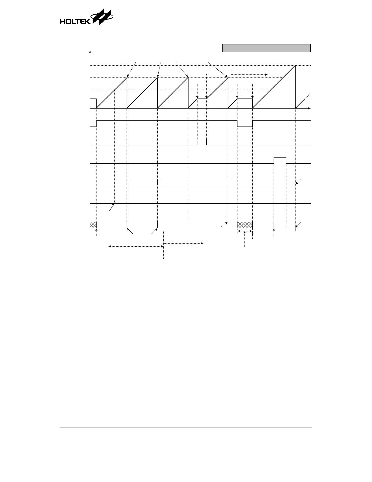
HT45F6530
AC Voltage Regulator Flash MCU
Counter Value
0x3FF
CCRA
CCRP
CTnON
CTnPAU
CTnPOL
CCRA Int. flag
CTMnAF
CCRP Int. flag
CTMnPF
CTMn O/P Pin
Output pin set to
initial Level Low if
CTnOC=0
CTMnPF not
generated
Here CTnIO [1:0] = 11
Toggle Output select
CTnCCLR = 1; CTnM [1:0] = 00
CCRA > 0 Counter cleared by CCRA value
CCRA=0
Stop
Output controlled by other
pin-shared function
Output Toggle with
CTMnAF flag
Resume
Pause
Output not affected by
CTMnAF flag. Remains High
until reset by CTnON bit
Note CTnIO [1:0] = 10
Active High Output select
Compare Match Output Mode – CTnCCLR=1 (n=0~1)
CCRA = 0
Counter overflow
Counter Restart
Output Inverts
Output Pin
Reset to Initial value
when CTnPOL is high
Time
No CTMnAF flag
generated on
CCRA overflow
Output does
not change
Note: 1. With CTnCCLR=1 a Comparator A match will clear the counter
2. The CTMn output pin is controlled only by the CTMnAF ag
3. The output pin is reset to its initial state by a CTnON bit rising edge
4. A CTMnPF ag is not generated when CTnCCLR=1
Rev. 1.00 68 August 29, 2018 Rev. 1.00 69 August 29, 2018
Page 69

HT45F6530
AC Voltage Regulator Flash MCU
Timer/Counter Mode
To select this mode, bits CTnM1 and CTnM0 in the CTMnC1 register should be set to 11
respectively. The Timer/Counter Mode operates in an identical way to the Compare Match Output
Mode generating the same interrupt flags. The exception is that in the Timer/Counter Mode the
CTMn output pin is not used. Therefore the above description and Timing Diagrams for the
Compare Match Output Mode can be used to understand its function. As the CTMn output pin is not
used in this mode, the pin can be used as a normal I/O pin or other pin-shared function.
PWM Output Mode
To select this mode, bits CTnM1 and CTnM0 in the CTMnC1 register should be set to 10
respectively. The PWM function within the CTMn is useful for applications which require functions
such as motor control, heating control, illumination control, etc. By providing a signal of fixed
frequency but of varying duty cycle on the CTMn output pin, a square wave AC waveform can be
generated with varying equivalent DC RMS values.
As both the period and duty cycle of the PWM waveform can be controlled, the choice of generated
waveform is extremely exible. In the PWM Output Mode, the CTnCCLR bit has no effect as the
PWM period. Both of the CCRA and CCRP registers are used to generate the PWM waveform, one
register is used to clear the internal counter and thus control the PWM waveform frequency, while
the other one is used to control the duty cycle. Which register is used to control either frequency
or duty cycle is determined using the CTnDPX bit in the CTMnC1 register. The PWM waveform
frequency and duty cycle can therefore be controlled by the values in the CCRA and CCRP registers.
An interrupt ag, one for each of the CCRA and CCRP, will be generated when a compare match
occurs from either Comparator A or Comparator P. The CTnOC bit in the CTMnC1 register is used
to select the required polarity of the PWM waveform while the two CTnIO1 and CTnIO0 bits are
used to enable the PWM output or to force the CTMn output pin to a xed high or low level. The
CTnPOL bit is used to reverse the polarity of the PWM output waveform.
• 10-bit CTMn, PWM Output Mode, Edge-aligned Mode, CTnDPX=0
CCRP 1~7 0
Period CCRP×128 1024
Duty CCRA
If f
=8MHz, CTMn clock source is f
SYS
The CTMn PWM output frequency=(f
/4, CCRP=4 and CCRA=128,
SYS
/4)/(4×128)=f
SYS
/2048=4kHz, duty=128/(4×128)=25%.
SYS
If the Duty value dened by the CCRA register is equal to or greater than the Period value, then the
PWM output duty is 100%.
• 10-bit CTMn, PWM Output Mode, Edge-aligned Mode, CTnDPX=1
CCRP 1~7 0
Period CCRA
Duty CCRP×128 1024
The PWM output period is determined by the CCRA register value together with the CTMn clock
while the PWM duty cycle is dened by the CCRP register value.
Page 70
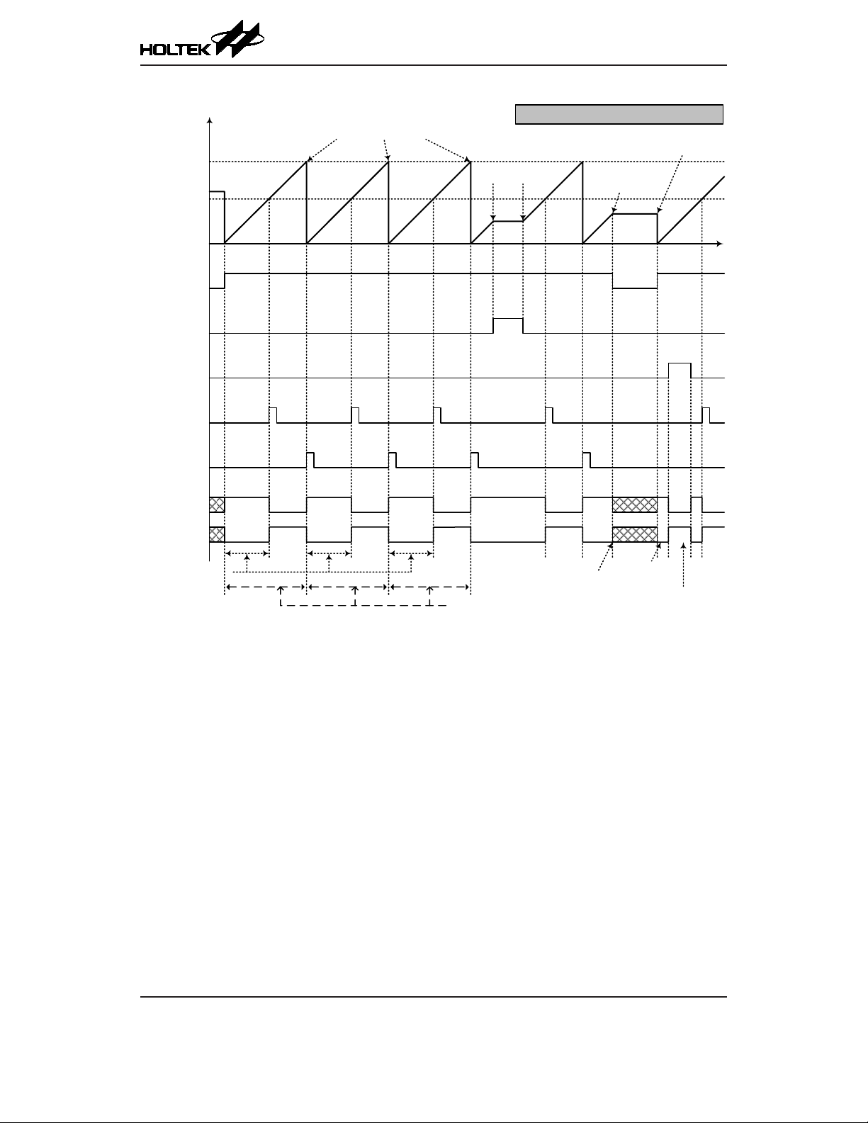
HT45F6530
AC Voltage Regulator Flash MCU
Counter Value
CCRP
CCRA
CTnON
CTnPAU
CTnPOL
CCRA Int. flag
CTMnAF
CCRP Int. flag
CTMnPF
CTMn O/P Pin
(CTnOC=1)
CTMn O/P Pin
(CTnOC=0)
Counter cleared by
CCRP
Pause
CTnDPX = 0; CTnM [1:0] = 10
Counter Reset when
CTnON returns high
Resume
Counter Stop if
CTnON bit low
Time
PWM Duty Cycle
set by CCRA
PWM Period set by CCRP
PWM Output Mode – CTnDPX=0 (n=0~1)
Note: 1. Here CTnDPX=0 – Counter cleared by CCRP
2. A counter clear sets the PWM Period
3. The internal PWM function continues running even when CTnIO[1:0]=00 or 01
4. The CTnCCLR bit has no inuence on PWM operation
Output controlled by
other pin-shared function
PWM resumes
operation
Output Inverts
when CTnPOL = 1
Rev. 1.00 70 August 29, 2018 Rev. 1.00 71 August 29, 2018
Page 71
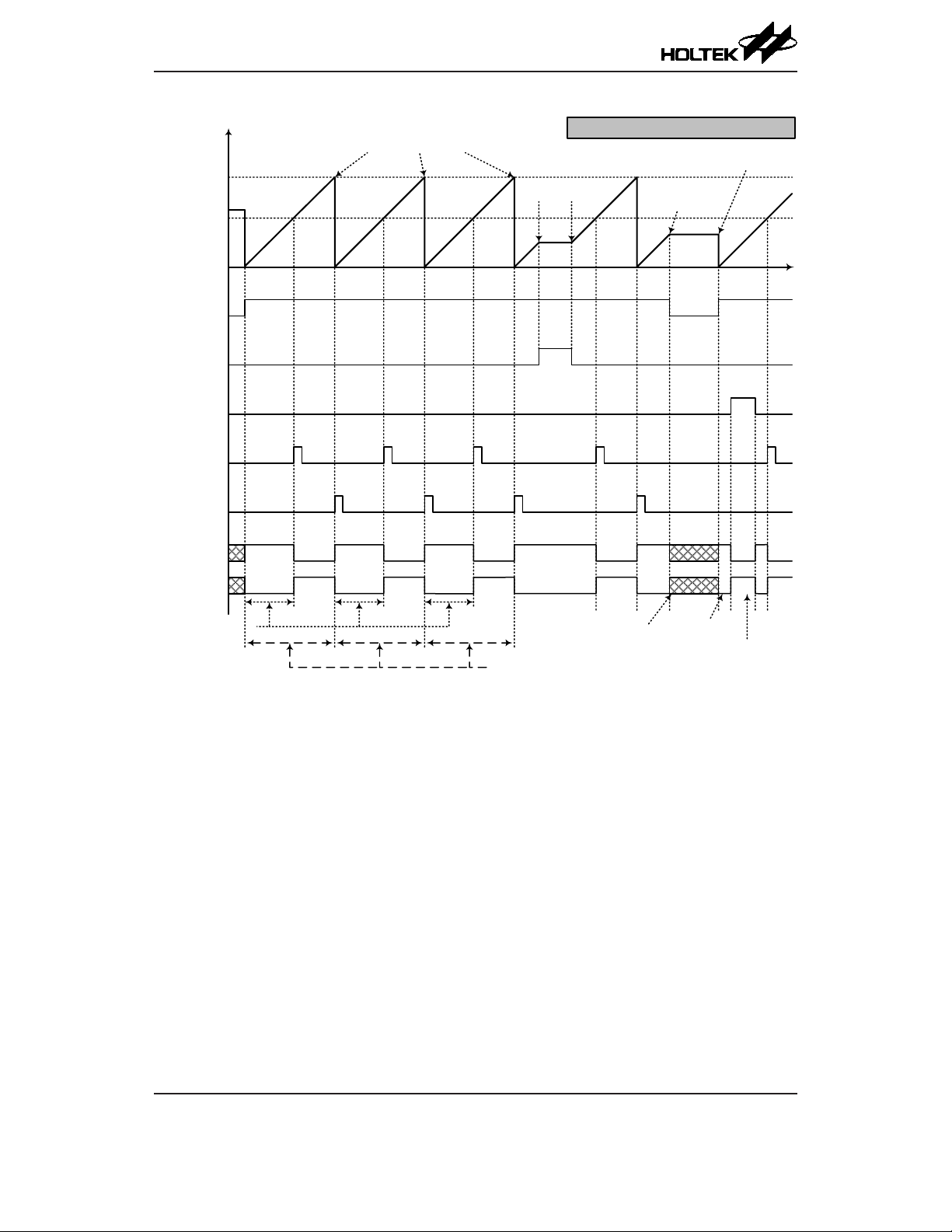
HT45F6530
AC Voltage Regulator Flash MCU
Counter Value
CCRA
CCRP
CTnON
CTnPAU
CTnPOL
CCRP Int. flag
CTMnPF
CCRA Int. flag
CTMnAF
CTMn O/P Pin
(CTnOC=1)
CTMn O/P Pin
(CTnOC=0)
Counter cleared by
CCRA
Pause
CTnDPX = 1; CTnM [1:0] = 10
Resume
Counter Stop if
CTnON bit low
Counter Reset when
CTnON returns high
Time
PWM Duty Cycle
set by CCRP
PWM Period set by CCRA
PWM Output Mode – CTnDPX=1 (n=0~1)
Note: 1. Here CTnDPX=1 – Counter cleared by CCRA
2. A counter clear sets the PWM Period
3. The internal PWM function continues even when CTnIO[1:0]=00 or 01
4. The CTnCCLR bit has no inuence on PWM operation
Output controlled by
other pin-shared function
PWM resumes
operation
Output Inverts
when CTnPOL = 1
Page 72
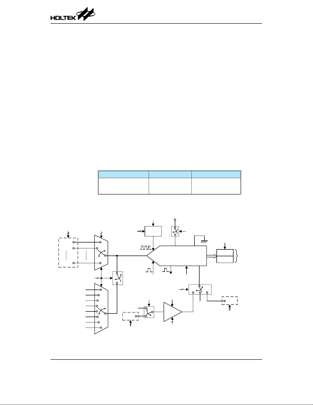
Analog to Digital Converter
The need to interface to real world analog signals is a common requirement for many electronic
systems. However, to properly process these signals by a microcontroller, they must first be
converted into digital signals by A/D converters. By integrating the A/D conversion electronic
circuitry into the microcontroller, the need for external components is reduced signicantly with the
corresponding follow-on benets of lower costs and reduced component space requirements.
A/D Converter Overview
This device contains a multi-channel analog to digital converter which can directly interface to
external analog signals, such as that from sensors or other control signals and convert these signals
directly into a 12-bit digital value. It also can convert the internal signals, such as the PGA output
divided voltage, the A/D power divided voltage and the OPA output voltage, into a 12-bit digital
value. The external or internal analog signal to be converted is determined by the SAINS3~SAINS0
bits together with the SACS3~SACS0 bits. When the external analog signal is to be converted,
the corresponding pin-shared control bits should first be properly configured and then desired
external channel input should be selected using the SAINS3~SAINS0 and SACS3~SACS0 bits.
Note that when the internal analog signal is to be converted, the external channel input signal will
automatically be disconnected regardless of the SACS bit eld value. More detailed information about
the A/D input signal is described in the “A/D Converter Control Registers” and “A/D Converter
Input Signals” sections respectively.
External Input Channels Internal Signals A/D Channel Select Bits
6: AN0~AN5
The accompanying block diagram shows the overall internal structure of the A/D converter, together
with its associated registers.
HT45F6530
AC Voltage Regulator Flash MCU
8: VDD, VDD/2, VDD/4,
VR, VR/2, VR/4,
V
, V
OPA0O
OPA1O
SAINS3~SAINS0,
SACS3~SACS0
Pin-shared
Selection
AN0
AN1
AN5
SAINS3~SAINS0
V
VDD/2
V
DD
V
VR/2
V
R
V
OPA0O
V
OPA1O
SACS3~SACS0
DD
/4
R
/4
f
SACKS2~
SACKS0
A/D Clock
V
BG
VREFI
Pin-shared
Selection
÷2
(N=0~7)
START ADBZ ADCEN
SAVRS1~SAVRS0
PGAIS
A/D Converter Structure
SYS
N
V
A/D Converter
ADPGAEN
V
RI
PGA
PGAGS1~PGAGS0
(Gain=1/2/3/4)
DD
ADCEN
V
SS
ADRFS
A/D Reference Voltage
V
DD
V
R
SADOL
SADOH
Pin-shared
Selection
A/D Data
Registers
VREF
Rev. 1.00 72 August 29, 2018 Rev. 1.00 73 August 29, 2018
Page 73
HT45F6530
AC Voltage Regulator Flash MCU
A/D Converter Register Description
Overall operation of the A/D converter is controlled using several registers. A read only register pair
exists to store the A/D converter data 12-bit value. The remaining three registers are control registers
which setup the operating and control function of the A/D converter.
Register Name
SADOL (ADRFS=0) D3 D2 D1 D0 — — — —
SADOL (ADRFS=1) D7 D6 D5 D4 D3 D2 D1 D0
SADOH (ADRFS=0) D11 D10 D9 D8 D7 D6 D5 D4
SADOH (ADRFS=1) — — — — D 11 D10 D9 D8
SADC0 START ADBZ ADCEN ADRFS SACS3 SACS2 SACS1 SACS0
SADC1 SAINS3 SAINS2 SAINS1 SAINS0 — SACKS2 SACKS1 SACKS0
SADC2 ADPGAEN — — PGAIS SAVRS1 SAVRS0 PGAGS1 PGAGS0
7 6 5 4 3 2 1 0
A/D Converter Register List
A/D Converter Data Registers – SADOL, SADOH
As this device contains an internal 12-bit A/D converter, it requires two data registers to store the
converted value. These are a high byte register, known as SADOH, and a low byte register, known
as SADOL. After the conversion process takes place, these registers can be directly read by the
microcontroller to obtain the digitised conversion value. As only 12 bits of the 16-bit register space
is utilised, the format in which the data is stored is controlled by the ADRFS bit in the SADC0
register as shown in the accompanying table. D0~D11 are the A/D conversion result data bits. Any
unused bits will be read as zero. Note that A/D data registers contents will be unchanged if the A/D
converter is disabled.
ADRFS
7 6 5 4 3 2 1 0 7 6 5 4 3 2 1 0
0 D11 D10 D9 D8 D7 D6 D5 D4 D3 D2 D1 D0 0 0 0 0
1 0 0 0 0 D11 D10 D9 D8 D7 D6 D5 D4 D3 D2 D1 D0
SADOH SADOL
A/D Converter Data Registers
Bit
A/D Converter Control Registers – SADC0, SADC1, SADC2
To control the function and operation of the A/D converter, three control registers known as
SADC0~SADC2 are provided. These 8-bit registers dene functions such as the selection of which
analog signal is connected to the internal A/D converter, the digitised data format, the A/D clock
source as well as controlling the start function and monitoring the A/D converter busy status. As the
device contains only one actual analog to digital converter hardware circuit, each of the external
or internal analog signal inputs must be routed to the converter. The SACS3~SACS0 bits in the
SADC0 register are used to determine which external channel input is selected to be converted.
The SAINS3~SAINS0 bits in the SADC1 register are used to determine that the analog signal to be
converted comes from the internal analog signal or external analog channel input. The A/D converter
also contains a programmable gain amplier, PGA, to generate the A/D converter internal reference
voltage. The overall operation of the PGA is controlled using the SADC2 register.
The relevant pin-shared function selection bits determine which pins on I/O Ports are used as analog
inputs for the A/D converter input and which pins are not to be used as the A/D converter input.
When the pin is selected to be an A/D input, its original function whether it is an I/O or other pin-
shared function will be removed. In addition, any internal pull-high resistor connected to the pin will
be automatically removed if the pin is selected to be an A/D converter input.
Page 74

HT45F6530
AC Voltage Regulator Flash MCU
• SADC0 Register
Bit 7 6 5 4 3 2 1 0
Name START ADBZ ADCEN ADRFS SACS3 SACS2 SACS1 SACS0
R/W R/W R R/W R/W R/W R/W R/W R/W
POR 0 0 0 0 0 0 0 0
Bit 7 START: Start the A/D conversion
0→1→0: Start
This bit is used to initiate an A/D conversion process. The bit is normally low but if set
high and then cleared low again, the A/D converter will initiate a conversion process.
Bit 6 ADBZ: A/D converter busy ag
0: No A/D conversion is in progress
1: A/D conversion is in progress
This read only ag is used to indicate whether the A/D conversion is in progress or
not. When the START bit is set from low to high and then to low again, the ADBZ ag
will be set to 1 to indicate that the A/D conversion is initiated. The ADBZ ag will be
cleared to 0 after the A/D conversion is complete.
Bit 5 ADCEN: A/D converter function enable control
0: Disable
1: Enable
This bit controls the A/D internal function. This bit should be set to one to enable
the A/D converter. If the bit is set low, then the A/D converter will be switched off
reducing the device power consumption. When the A/D converter function is disabled,
the contents of the A/D data register pair known as SADOH and SADOL will be
unchanged.
Bit 4 ADRFS: A/D converter data format select
0: A/D converter data format → SADOH=D[11:4]; SADOL=D[3:0]
1: A/D converter data format → SADOH=D[11:8]; SADOL=D[7:0]
This bit controls the format of the 12-bit converted A/D value in the two A/D data
registers. Details are provided in the A/D data register section.
Bit 3~0 SACS3~SACS0: A/D converter external analog channel input select
0000: AN0
0001: AN1
0010: AN2
0011: AN3
0100: AN4
0101: AN5
0110~1111: undened, input oating if selected
These bits are used to select which external analog input channel is to be converted.
When the external analog input channel is selected, the SAINS bit eld must be set to
“0000”, “0100” or “11xx”. Details are summarised in the “A/D Converter Input Signal
Selection” table.
Rev. 1.00 74 August 29, 2018 Rev. 1.00 75 August 29, 2018
Page 75

HT45F6530
AC Voltage Regulator Flash MCU
• SADC1 Register
Bit 7 6 5 4 3 2 1 0
Name SAINS3 SAINS2 SAINS1 SAINS0 — SACKS2 SACKS1 SACKS0
R/W R/W R/W R/W R/W — R/W R/W R/W
POR 0 0 0 0 — 0 0 0
Bit 7~4 SAINS3~SAINS0: A/D converter input signal select
0000: External source – External analog channel input, ANn
0001: Internal source – Internal A/D converter power supply voltage V
0010: Internal source – Internal A/D converter power supply voltage VDD/2
0011: Internal source – Internal A/D converter power supply voltage VDD/4
0100: External source – External analog channel input, ANn
0101: Internal source – Internal A/D converter PGA output voltage V
0110: Internal source – Internal A/D converter PGA output voltage VR/2
0111: Internal source – Internal A/D converter PGA output voltage VR/4
1000: Internal source – Internal Operational Amplier 0 output voltage, V
1001: Internal source – Internal Operational Amplier 1 output voltage, V
1010~1011: Reserved, connected to ground
1100~1111: External input – External analog channel input, ANn
When the internal analog signal is selected to be converted, the external channel signal
input will automatically be switched off regardless of the SACS eld value.
Bit 3 Unimplemented, read as “0”
Bit 2~0 SACKS2~SACKS0: A/D conversion clock source select
000: f
SYS
001: f
010: f
011: f
100: f
101: f
110: f
111: f
These three bits are used to select the clock source for the A/D converter.
SYS
SYS
SYS
SYS
SYS
SYS
SYS
/2
/4
/8
/16
/32
/64
/128
DD
R
OPA0O
OPA1O
• SADC2 Register
Bit 7 6 5 4 3 2 1 0
Name ADPGAEN — — PGAIS SAVRS1 SAVRS0 PGAGS1 PGAGS0
R/W R/W — — R/W R/W R/W R/W R/W
POR 0 — — 0 0 0 0 0
Bit 7 ADPGAEN: PGA enable/disable control
0: Disable
1: Enable
When the PGA output VR is selected as A/D converter input or A/D converter
reference voltage, the PGA must to be enabled by setting this bit high. Otherwise the
PGA should to be disabled by clearing this bit to zero to conserve the power.
Bit 6~5 Unimplemented, read as “0”
Bit 4 PGAIS: PGA input (VRI) select
0: External VREFI pin
1: Internal independent reference voltage, V
BG
This bit is used to select the PGA input source. When the internal voltage independent
reference VBG is selected, the external voltage on VREFI pin will automatically be
switched off.
Page 76

Bit 3~2 SAVRS1~SAVRS0: A/D converter reference voltage select
00: Internal A/D converter power, V
01: External VREF pin
1x: Internal PGA output voltage, V
These bits are used to select the A/D converter reference voltage source. When the
internal reference voltage source is selected, the reference voltage derived from the
external VREF pin will automatically be switched off.
Bit 1~0 PGAGS1~PGAGS0: PGA gain select
00: Gain=1
01: Gain=2
10: Gain=3
11: Gain=4
A/D Converter Reference Voltage
The actual reference voltage supply to the A/D converter can be supplied from the positive power
supply pin, VDD, or from an external reference source supplied on pin VREF, or from the internal
PGA output voltage, VR. The desired selection is made using the SAVRS1 and SAVRS0 bits in the
SADC2 register. When the SAVRS bit eld is set to “00”, the A/D converter reference voltage will
come from the VDD pin. If the SAVRS bit eld is set to “01”, the A/D converter reference voltage
will come from the VREF pin. Otherwise, the A/D converter reference voltage will come from the
PGA output, VR. As the VREF pin is pin-shared with other functions, when the VREF pin is selected
as the reference voltage supply pin, the VREF pin-shared function control bits should be properly
congured to disable other pin functions. However, if the internal reference signal, VDD or VR, is
selected as the A/D converter reference source, the external reference input from the VREF pin
will automatically be switched off by the hardware. The analog input values must not be allowed to
exceed the value of the selected reference voltage, V
In addition, the A/D converter also has a VREFI pin which is one of PGA inputs for A/D converter
reference. To select this PGA input signal, the PGAIS bit in the SADC2 register must be cleared to
zero and the relevant pin-shared control bits should be properly congured. However, the PGA input
can be also supplied from the internal independent reference voltage, VBG. If the internal voltage
VBG is selected as the PGA input source, the external voltage on the VREFI pin will automatically be
switched off by the hardware. The PGA input voltage can be amplied through a programmable gain
amplier, PGA, which is controlled by the ADPGAEN bit in the SADC2 register. The PGA gain can
be equal to 1, 2, 3 or 4.
SAVRS[1:0] Reference Description
00 V
01 VREF pin External A/D converter reference pin VREF
1x V
A/D Converter Reference Voltage Selection
AC Voltage Regulator Flash MCU
DD
R
.
REF
Internal A/D converter power supply voltage
DD
Internal A/D converter PGA output voltage
R
HT45F6530
A/D Converter Input Signals
All the external A/D analog channel input pins are pin-shared with the I/O pins as well as other
functions. The corresponding control bits for each A/D external input pin in the PxS1 and PxS0
registers determine whether the input pins are setup as A/D converter analog inputs or whether
they have other functions. If the pin is setup to be as an A/D analog channel input, the original pin
functions will be disabled. In this way, pins can be changed under program control to change their
function between A/D inputs and other functions. All pull high resistors, which are setup through
register programming, will be automatically disconnected if the pins are setup as A/D inputs. Note
that it is not necessary to rst setup the A/D pin as an input in the port control register to enable the
Rev. 1.00 76 August 29, 2018 Rev. 1.00 77 August 29, 2018
Page 77

HT45F6530
AC Voltage Regulator Flash MCU
A/D input as when the pin-shared function control bits enable an A/D input, the status of the port
control register will be overridden.
If the SAINS3~SAINS0 bits are set to “0000”, “0100”, or “1100~1111”, the external analog channel
input is selected to be converted and the SACS3~SACS0 bits can determine which actual external
channel is selected to be converted. If the SAINS3~SAINS0 bits are set to “0001~0011”, the VDD
voltage with a specic ratio of 1, 1/2 or 1/4 is selected to be converted. If the SAINS3~SAINS0 bits
are set to “0101~0111”, the PGA output voltage with a specic ratio of 1, 1/2 or 1/4 is selected to be
converted. If the SAINS3~SAINS0 bits are set to “1000~1001”, the OCP operational amplier 0 or
1 output voltage is selected to be converted. Note that when the internal analog signal is selected to
be converted, then the external channel signal input will automatically be switched off regardless of
the SACS eld value. It will prevent the external channel input from being connected together with
the internal analog signal.
SAINS[3:0] SACS[3:0] Input Signals Description
0000, 0100,
110 0~1111
0001 xxxx V
0010 xxxx VDD/2 Internal A/D converter power supply voltage/2
0011 xxxx VDD/4 Internal A/D converter power supply voltage/4
0101 xxxx V
0110 xxxx VR/2 Internal A/D converter PGA output voltage/2
0111 xxxx VR/4 Internal A/D converter PGA output voltage/4
1000 xxxx V
1001 xxxx V
1010~1011 xxxx GND Reserved, connected to ground.
0000~0101 AN0~AN5 External pin analog input
011 0~1111 — Floating, no external channel is selected
OPA0O
OPA1O
DD
R
Internal A/D converter power supply voltage
Internal A/D converter PGA output voltage
Internal OCP Operational Amplier 0 output voltage
Internal OCP Operational Amplier 1 output voltage
A/D Converter Operation
The START bit in the SADC0 register is used to start the AD conversion. When the microcontroller sets
this bit from low to high and then low again, an analog to digital conversion cycle will be initiated.
The ADBZ bit in the SADC0 register is used to indicate whether the analog to digital conversion
process is in progress or not. This bit will be automatically set to 1 by the microcontroller after an
A/D conversion is successfully initiated. When the A/D conversion is complete, the ADBZ will be
cleared to 0. In addition, the corresponding A/D interrupt request ag will be set in the interrupt
control register, and if the interrupts are enabled, an appropriate internal interrupt signal will be
generated. This A/D internal interrupt signal will direct the program flow to the associated A/D
internal interrupt address for processing. If the A/D internal interrupt is disabled, the microcontroller
can poll the ADBZ bit in the SADC0 register to check whether it has been cleared as an alternative
method of detecting the end of an A/D conversion cycle.
The clock source for the A/D converter, which originates from the system clock f
chosen to be either f
the SACKS2~SACKS0 bits in the SADC1 register. Although the A/D clock source is determined
by the system clock f
clock source speed range that can be selected. As the recommended range of permissible A/D clock
period, t
as the system clock operates at a frequency of 8MHz, the SACKS2~SACKS0 bits should not be set
to 000, 001 or 111. Doing so will give A/D clock periods that are less than the minimum or larger
, is from 0.5μs to 10μs, care must be taken for system clock frequencies. For example,
ADCK
"x": Don't care.
A/D Converter Input Signal Selection
SYS
or a subdivided version of f
SYS
and by bits SACKS2~SACKS0, there are some limitations on the A/D
SYS
. The division ratio value is determined by
SYS
, can be
Page 78

HT45F6530
AC Voltage Regulator Flash MCU
than the maximum A/D clock period which may result in inaccurate A/D conversion values. Refer to
the following table for examples, where values marked with an asterisk * show where special care
must be taken, as the values may be exceeding the specied A/D Clock Period range.
A/D Clock Period (t
SACKS[2:0]
f
SYS
1MHz 1μs 2μs 4μs 8μs 16μs * 32μs * 64μs * 128μs *
2MHz 500ns 1μs 2μs 4μs 8μs 16μs * 32μs * 64μs *
4MHz 250ns * 500ns 1μs 2μs 4μs 8μs 16μs * 32μs *
8MHz 125ns * 250ns * 500ns 1μs 2μs 4μs 8μs 16μs *
=000
(f
SYS
)
SACKS[2:0]
=001
(f
/2)
SYS
SACKS[2:0]
=010
(f
/4)
SYS
SACKS[2:0]
=011
(f
/8)
SYS
SACKS[2:0]
A/D Clock Period Examples
Controlling the power on/off function of the A/D converter circuitry is implemented using the
ADCEN bit in the SADC0 register. This bit must be set high to power on the A/D converter. When
the ADCEN bit is set high to power on the A/D converter internal circuitry a certain delay, as
indicated in the timing diagram, must be allowed before an A/D conversion is initiated. Even if
no pins are selected for use as A/D inputs, if the ADCEN bit is high, then some power will still be
consumed. In power conscious applications it is therefore recommended that the ADCEN is set low
to reduce power consumption when the A/D converter function is not being used.
(f
=100
SYS
ADCK
/16)
)
SACKS[2:0]
(f
=101
SYS
/32)
SACKS[2:0]
=110
(f
/64)
SYS
SACKS[2:0]
=111
(f
/128)
SYS
Conversion Rate and Timing Diagram
A complete A/D conversion contains two parts, data sampling and data conversion. The data
sampling which is dened as t
clock cycles. Therefore a total of 16 A/D clock cycles for an external input A/D conversion which is
ADCEN
START
ADBZ
SACS[3:0]
(SAINS[3:0]=0000)
dened as t
The accompanying diagram shows graphically the various stages involved in an external channel
input signal analog to digital conversion process and its associated timing. After an A/D conversion
process has been initiated by the application program, the microcontroller internal hardware will
begin to carry out the conversion, during which time the program can continue with other functions.
The time taken for the A/D conversion is 16 t
period.
off on off on
0011B 0010B 0000B 0001B
A/D channel
switch
ADC
t
ON2ST
are necessary.
Maximum single A/D conversion rate=A/D clock period/16
A/D sampling time
t
ADS
Start of A/D conversion Start of A/D conversion Start of A/D conversion
End of A/D
conversion
t
ADC
A/D conversion time
A/D Conversion Timing – External Channel Input
takes 4 A/D clock cycles and the data conversion takes 12 A/D
ADS
clock cycles where t
ADCK
A/D sampling time
t
ADS
End of A/D
conversion
t
ADC
A/D conversion time
is equal to the A/D clock
ADCK
t
ADC
A/D conversion time
Rev. 1.00 78 August 29, 2018 Rev. 1.00 79 August 29, 2018
Page 79

HT45F6530
AC Voltage Regulator Flash MCU
Summary of A/D Conversion Steps
The following summarises the individual steps that should be executed in order to implement an A/D
conversion process.
• Step 1
Select the required A/D conversion clock by correctly programming bits SACKS2~SACKS0 in
the SADC1 register.
• Step 2
Enable the A/D by setting the ADCEN bit in the SADC0 register to one.
• Step 3
Select which signal is to be connected to the internal A/D converter by correctly conguring the
SAINS3~SAINS0 bits in the SADC1 register.
Select the external channel input to be converted, go to Step 4.
Select the internal analog signal to be converted, go to Step 5.
• Step 4
If the A/D input signal comes from the external channel input selected by conguring the SAINS
bit eld, the corresponding pins should be congured as A/D input function by conguring the
relevant pin-shared function control bits. The desired analog channel then should be selected by
conguring the SACS bit eld. After this step, go to Step 6.
• Step 5
If the A/D input signal comes from the internal analog signal, the SAINS bit field should be
properly configured and then the external channel input will automatically be disconnected
regardless of the SACS bit eld value. After this step, go to Step 6.
• Step 6
Select the reference voltage source by configuring the SAVRS1~SAVRS0 bits in the SADC2
register.
Select the PGA input signal and the desired PGA gain and enable the PGA if the PGA output
voltage, VR, is selected as the A/D converter reference voltage.
• Step 7
Select A/D converter output data format by setting the ADRFS bit in the SADC0 register.
• Step 8
If A/D conversion interrupt is used, the interrupt control registers must be correctly congured
to ensure the A/D interrupt function is active. The master interrupt control bit, EMI, and the A/D
conversion interrupt control bit, ADE, must both be set high in advance.
• Step 9
The A/D conversion procedure can now be initialized by setting the START bit from low to high
and then low again.
• Step 10
If A/D conversion is in progress, the ADBZ flag will be set high. After the A/D conversion
process is complete, the ADBZ flag will go low and then the output data can be read from
SADOH and SADOL registers.
Note: When checking for the end of the conversion process, if the method of polling the ADBZ bit
in the SADC0 register is used, the interrupt enable step above can be omitted.
Page 80
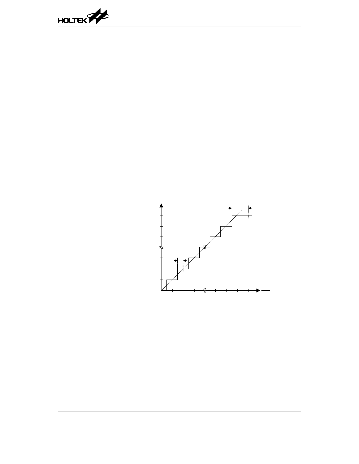
Programming Considerations
During microcontroller operations where the A/D converter is not being used, the A/D internal
circuitry can be switched off to reduce power consumption, by clearing bit ADCEN to 0 in the
SADC0 register. When this happens, the internal A/D converter circuits will not consume power
irrespective of what analog voltage is applied to their input lines. If the A/D converter input lines are
used as normal I/Os, then care must be taken as if the input voltage is not at a valid logic level, then
this may lead to some increase in power consumption.
A/D Conversion Function
As the device contains a 12-bit A/D converter, its full-scale converted digitised value is equal
to 0FFFH. Since the full-scale analog input value is equal to the actual A/D converter reference
voltage, V
The A/D Converter input voltage value can be calculated using the following equation:
The diagram shows the ideal transfer function between the analog input value and the digitised
output value for the A/D converter. Except for the digitised zero value, the subsequent digitised
values will change at a point 0.5 LSB below where they would change without the offset, and the
last full scale digitised value will change at a point 1.5 LSB below the V
V
voltage is the actual A/D converter reference voltage determined by the SAVRS eld.
REF
, this gives a single bit analog input value of V
REF
A/D input voltage=A/D output digital value×(V
HT45F6530
AC Voltage Regulator Flash MCU
divided by 4096.
REF
1 LSB=V
REF
÷4096
÷4096)
REF
level. Note that here the
REF
FFFH
FFEH
FFDH
A/D Conversion
Result
03H
02H
01H
0 1 2 3 4093 4094 4095 4096
0.5 LSB
Ideal A/D Transfer Function
A/D Conversion Programming Examples
The following two programming examples illustrate how to setup and implement an A/D conversion.
In the rst example, the method of polling the ADBZ bit in the SADC0 register is used to detect
when the conversion cycle is complete, whereas in the second example, the A/D interrupt is used to
determine when the conversion is complete.
Example: Using an ADBZ polling method to detect the end of conversion
clr ADE ; disable ADC interrupt
mo v a,03H ; se le ct f
movSADC1,a ;signalcomesfromexternalchannel
mova,00H ;selectVDD as the A/D reference voltage source
movSADC2,a
/8 as A/D clock and A/D input
SYS
Analog Input Voltage
1.5 LSB
V
REF
4096
Rev. 1.00 80 August 29, 2018 Rev. 1.00 81 August 29, 2018
Page 81

HT45F6530
AC Voltage Regulator Flash MCU
mova,0c0H ;setupPAS1tocongurepinAN0
movPAS1
mova,20h ;enableA/Dconverter,selectdefaultdataformatandconnectAN0
; channel to A/D converter
movSADC0,a
:
:
start_conversion:
clrSTART ;highpulseonstartbittoinitiateconversion
setSTART ;resetA/D
clrSTART ;startA/D
polling_EOC:
szADBZ ;polltheSADC0registerADBZbittodetectendofA/Dconversion
jmppolling_EOC ;continuepolling
mova,SADOL ;readlowbyteconversionresultvalue
movSADOL_buffer,a ;saveresulttouserdenedregister
mova,SADOH ;readhighbyteconversionresultvalue
movSADOH_buffer,a ;saveresulttouserdenedregister
:
:
jmpstart_conversion ;startnextA/Dconversion
Example: Using the interrupt method to detect the end of conversion
clr ADE ; disable ADC interrupt
mo v a,03H ; se le ct f
movSADC1,a ;signalcomesfromexternalchannel
mova,00H ;selectVDD as the A/D reference voltage source
movSADC2,a
mova,0c0H ;setupPAS1tocongurepinAN0
movPAS1
mova,20h ;enableA/Dconverter,selectdefaultdataformatandconnectAN0
; channel to A/D converter
movSADC0,a
:
:
start_conversion:
clrSTART ;highpulseonSTARTbittoinitiateconversion
setSTART ;resetA/D
clrSTART ;startA/D
clrADF ;clearADCinterruptrequestag
set ADE ; enable ADC interrupt
setEMI ;enableglobalinterrupt
:
:
; ADC interrupt service routine
ADC_ISR:
movacc_stack,a ;saveACCtouserdenedmemory
mova,STATUS
movstatus_stack,a ;saveSTATUStouserdenedmemory
:
:
mova,SADOL ;readlowbyteconversionresultvalue
movSADOL_buffer,a ;saveresulttouserdenedregister
mova,SADOH ;readhighbyteconversionresultvalue
movSADOH_buffer,a ;saveresulttouserdenedregister
:
:
EXIT_INT_ISR:
mova,status_stack
movSTATUS,a ;restoreSTATUSfromuserdenedmemory
mova,acc_stack ;restoreACCfromuserdenedmemory
reti
/8 as A/D clock and A/D input
SYS
Page 82

Over Current Protection – OCP
The device includes two over current protection functions which provide a protection mechanism
for applications. Each OCP function consists of one fully integrated Operational Amplier and one
Comparator as well as one 12-bit R2R D/A Converter with buffer. The Operational Amplier can be
used for signal amplication according to specic user requirements. The 12-bit D/A Converter can
provide an accurate reference voltage to the negative input of Comparator. The Comparator is used
to compare two analog voltages and provide an output based on their difference and generate an
interrupt to indicate a specic current condition has occurred if the corresponding interrupt control is
enabled.
Over Current Protection Operation
The over current protection circuit is used to prevent the input current from being in an unexpected
level range. The current on the OPAnP or OPAnN pin is converted to a voltage and then amplied
by the OCP Operational Amplier n with adjustable bandwidth. After the current is converted and
amplied to a specic voltage level, it will be compared with a reference voltage provided by the
12-bit OCP D/A Converter n.
The OCP Operational Amplifier n and the OCP Comparator n can be configured to operate in
the normal operating mode or input offset calibration mode determined by the OnOFM bit in the
OPnVOS register and the CnOFM bit in the CMPnVOS register respectively. The OCP Operational
Amplier n output signal can also be directly output on the OPAnO pin, or internally connected
to the A/D converter input. A buffer within the OCP D/A Converter n can enhance output driving
capability. Its reference voltage can be supplied by VDD or external VRnEXT pin, selected by
the DACnVRS bit in the DACnC register. The OCP Comparator n output bit, CMPnO, indicates
whether a user-dened current condition occurs or not.
If the CMPnO bit changes state from low to high, made by the specic voltages on OCP Comparator
n inputs and by the corresponding condition of the CnPOL bit, a one shot signal will be generated to
trigger an OCPn interrupt request. It is important to note that, only the rising edge of CMPnO bit can
trigger an OCPn interrupt request, so the CnPOL bit must be properly congured according to user’s
application requirements.
HT45F6530
AC Voltage Regulator Flash MCU
Rev. 1.00 82 August 29, 2018 Rev. 1.00 83 August 29, 2018
Page 83
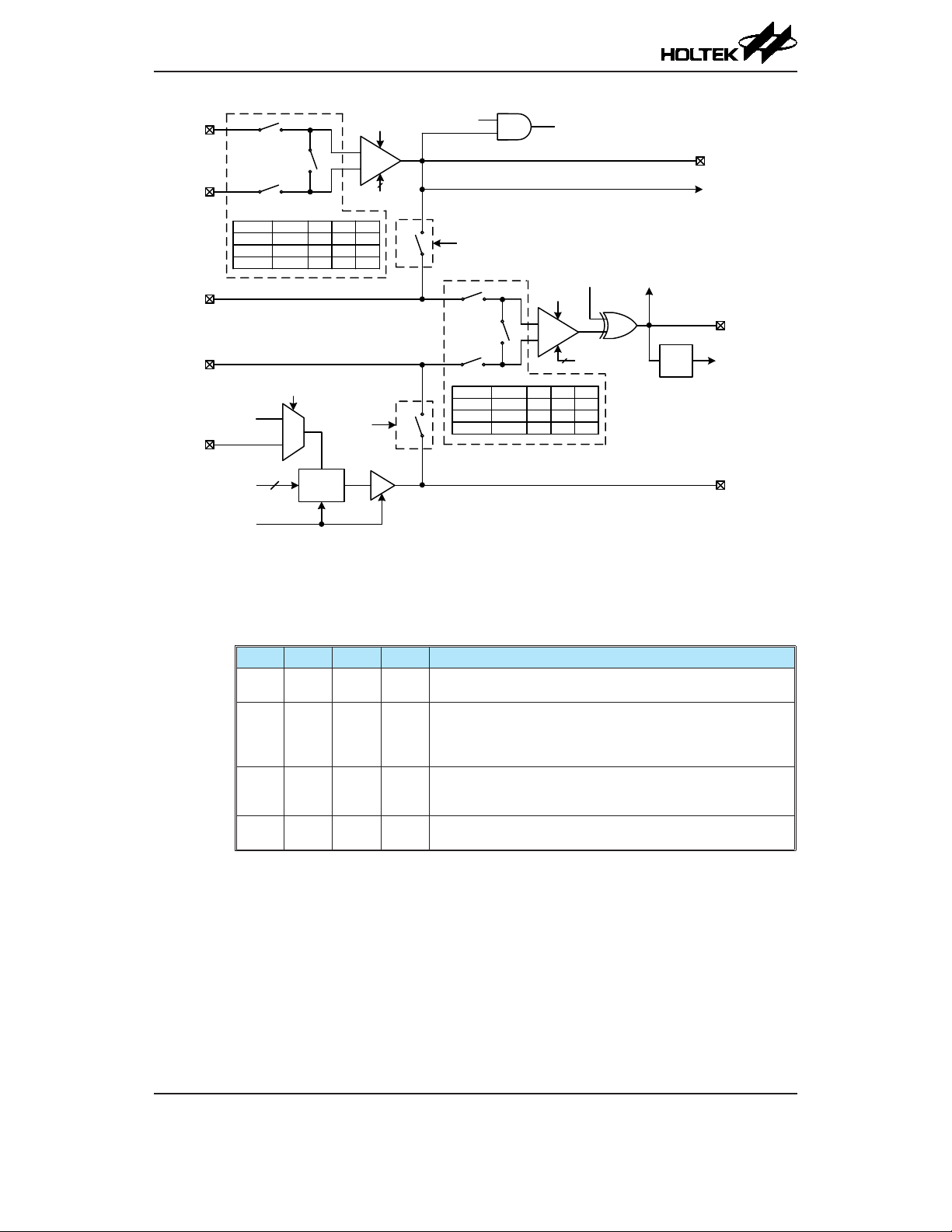
HT45F6530
AC Voltage Regulator Flash MCU
S7
S6
OnOFM
Sn7
S3
S4
CnOFM
0
1
1
x: Don't care
S5
CnRSP S3
x
0
1
OPnOUT
CMPnEN
+
CMP
-
S4 S5
ON
ON
OFF
ON
ON
OFF
CnPOL
CNVTn[1:0]
OFF
ON
ON
CMPnO
one
shot
OPAnO
To A/D converter
CMPnO
OCPn Interrupt
BUF_OUTn
OPAnP
OPAnN
CMPnP
CMPnN
VRnEXT
OnOFM
x: Don't care
V
D[11:0]
DACnEN
0
1
1
DD
S0
S2
S1
OnRSP S0
x
0
1
DACnVRS
ON
OFF
ON
R2R
D/A
OPnEN
OPnBW[1:0]
S1 S2
ON
OFF
ON
ON
OFF
ON
Sn6
+
OPA
-
Note: In applications, the BUF_OUTn function should be rst selected by properly conguring the corresponding
pin-shared function register before the DACnEN bit is set high.
Over Current Protection Block Diagram (n=0~1)
The above circuit can be combined to associative functions via switches S6 and S7 by controlling
the Sn6 and Sn7 bits. The following table illustrates all implemented functions.
Sn6 Sn7 S6 S7 Implemented Functions
0 0 OFF OFF
0 1 OFF ON
1 0 ON OFF
1 1 ON ON
Implemented Function Summary
Over Current Protection Registers
Overall operation of the over current protection is controlled using a series of registers. The DAnH
and DAnL registers are used to setup the OCP D/A Converter n output control code. The DACnC
register is used for OCP D/A Converter n enable or disable control and reference input selection as
well as switches on/off control. The OPnC and OPnVOS registers are used for overall control of the
OCP Operational Amplier n, including enable/disable control, operating mode selection, bandwidth
setup and so on. The CMPnC and CMPnVOS registers are related to overall control of the OCP
Comparator n, such as enable/disable control, input offset calibration related setup, response time
selection, etc.
Independent operational amplier; Independent comparator;
Independent D/A converter
Independent D/A converter;
Combine to a function of operational amplier and comparator:
the operational amplier amplies a signal and then the
comparator compares it with the external signals
Independent operational amplier
Combine to an over voltage protection function of D/A converter
and comparator
Combine to a complete over current protection function of
operational amplier, comparator and D/A converter
Page 84
HT45F6530
AC Voltage Regulator Flash MCU
Register
Name
DAnH — — — — D11 D10 D9 D8
DAnL D7 D6 D5 D4 D3 D2 D1 D0
DACnC DACnEN DACnVRS — — — — Sn7 Sn6
OPnC OPnOUT OPnEN — — — — OPnBW1 OPnBW0
OPnVOS OnOFM OnRSP OnOF5 OnOF4 OnOF3 OnOF2 OnOF1 OnOF0
CMPnC — CMPnEN CnPOL CMPnO CNVTn1 CNVTn0 — —
CMPnVOS — CnOFM CnRSP CnOF4 CnOF3 CnOF2 CnOF1 CnOF0
7 6 5 4 3 2 1 0
Over Current Protection Register List (n=0~1)
Bit
D/A Converter Registers – DAnH, DAnL, DACnC
• DAnH Register
Bit 7 6 5 4 3 2 1 0
Name — — — — D 11 D10 D9 D8
R/W — — — — R/W R/W R/W R/W
POR — — — — 0 0 0 0
Bit 7~4 Unimplemented, read as “0”
Bit 3~0 D11~D8: OCP D/A Converter n output control code high byte
• DAnL Register
Bit 7 6 5 4 3 2 1 0
Name D7 D6 D5 D4 D3 D2 D1 D0
R/W R/W R/W R/W R/W R/W R/W R/W R/W
POR 0 0 0 0 0 0 0 0
Bit 7~0 D7~D0: OCP D/A Converter n output control code low byte
Writing this register will only write the data to a shadow buffer and writing the DAnH
register will simultaneously copy the shadow buffer data to the DAnL register.
OCP D/A Converter n Output=(D/A Converter n reference voltage/212)×D[11:0]
• DACnC Register
Bit 7 6 5 4 3 2 1 0
Name DACnEN DACnVRS — — — — Sn7 Sn6
R/W R/W R/W — — — — R/W R/W
POR 0 0 — — — — 0 0
Bit 7 DACnEN: OCP D/A Converter n enable or disable control bit
0: Disable
1: Enable
Note that in applications the BUF_OUTn function should be rst selected by properly
conguring the corresponding pin-shared function register before the DACnEN bit is
set high.
Bit 6 DACnVRS: OCP D/A Converter n reference voltage selection
0: From V
DD
1: From VRnEXT pin
Bit 5~2 Unimplemented, read as “0”
Bit 1 Sn7: Switch S7 control
0: Off
1: On
Rev. 1.00 84 August 29, 2018 Rev. 1.00 85 August 29, 2018
Page 85
HT45F6530
AC Voltage Regulator Flash MCU
When the switch S7 is on by setting this bit high, the operational amplier n output
signal will be internally connected to the comparator n positive input. Therefore the
CMPnP pin function should be rst switched off by properly conguring the relevant
pin-shared control bits to avoid signal coniction.
Bit 0 Sn6: Switch S6 control
0: Off
1: On
When the switch S6 is on by setting this bit high, the D/A converter n output signal
will be internally connected to the comparator n negative input. Therefore the CMPnN
pin function should be first switched off by properly configuring the relevant pin-
shared control bits to avoid signal coniction.
Operational Amplier Registers – OPnC, OPnVOS
• OPnC Register
Bit 7 6 5 4 3 2 1 0
Name OPnOUT OPnEN — — — — OPnBW1 OPnBW0
R/W R R/W — — — — R/W R/W
POR 0 0 — — — — 0 0
Bit 7 OPnOUT: OCP Operational Amplier n digital output bit, positive logic (read only)
When the OCP Operational Amplier n is disabled, this bit will be cleared to zero.
When the OnOFM bit is set high, the OPnOUT bit is defined as OCP Operational
Amplier n output status, refer to the “Operational Amplier Input Offset Calibration”
section for the detailed offset calibration procedures.
Bit 6 OPnEN: OCP Operational Amplier n enable or disable control bit
0: Disable
1: Enable
Bit 5~2 Unimplemented, read as “0”
Bit 1~0 OPnBW1~OPnBW0: OCP Operational Amplier n bandwidth control bits
Refer to “Operational Amplier Electrical Characteristics” for details.
• OPnVOS Register
Bit 7 6 5 4 3 2 1 0
Name OnOFM OnRSP OnOF5 OnOF4 OnOF3 OnOF2 OnOF1 OnOF0
R/W R/W R/W R/W R/W R/W R/W R/W R/W
POR 0 0 1 0 0 0 0 0
Bit 7 OnOFM: OCP Operational Amplier n operating mode selection
0: Normal operating mode
1: Input offset calibration mode
This bit is used to select the OCP Operational Amplier n operating mode. If the bit
is zero the OCP Operational Amplier n will operate normally. The OCP Operational
Amplifier n will enter the offset calibration mode if this bit is set high. Refer to
the “Operational Amplifier Input Offset Calibration” section for the detailed offset
alibration procedures.
c
Bit 6 OnRSP: OCP Operational Amplier n input offset voltage calibration reference
selection
0: From OPAnN pin
1: From OPAnP pin
This bit is used to select the OCP Operational Amplifier n input offset calibration
reference. When the OCP Operational Amplier n is in the offset calibration mode,
the calibration reference input can come from the OCP Operational Amplier n inputs,
OPAnN or OPAnP, determined by this bit. This bit is only available when the OCP
Operational Amplier n operates in offset calibration mode.
Page 86
HT45F6530
AC Voltage Regulator Flash MCU
Bit 5~0 OnOF5~OnOF0: OCP Operational Amplier n input offset voltage calibration control
bits
These bits are used to calibrate the input offset according to the selected reference
input when the OCP Operational Amplifier n is in the offset calibration mode.
More detailed information is described in the “Operational Amplifier Input Offset
Calibration” section.
Comparator Registers – CMPnC, CMPnVOS
• CMPnC Register
Bit 7 6 5 4 3 2 1 0
Name — CMPnEN CnPOL CMPnO CNVTn1 CNVTn0 — —
R/W — R/W R/W R R/W R/W — —
POR — 0 0 0 0 0 — —
Bit 7 Unimplemented, read as “0”
Bit 6 CMPnEN: OCP Comparator n enable or disable control
0: Disable
1: Enable
This bit is used to control the OCP Comparator n on/off. The OCP Comparator n
output will be set low when this bit is cleared to zero. Therefore, CMPnO=0 when
CnPOL=0, or CMPnO=1 when CnPOL=1.
Bit 5 CnPOL: OCP Comparator n output polarity control
0: Non-invert
1: Invert
This bit is used to control the OCP Comparator n output polarity. If the bit is zero
then the OCP Comparator n output bit, CMPnO, will reect the non-inverted output
condition of the OCP Comparator n. If the bit is high the OCP Comparator n output bit
will be inverted.
Bit 4 CMPnO: OCP Comparator n output bit
If CnPOL=0,
0: CMPnP < CMPnN
1: CMPnP > CMPnN
If CnPOL=1,
0: CMPnP > CMPnN
1: CMPnP < CMPnN
This bit stores the OCP Comparator n output bit. The polarity of the bit is determined by
the voltages on the OCP Comparator n inputs and by the condition of the CnPOL bit.
Bit 3~2 CNVTn1~CNVTn0: OCP Comparator n response time selection
These bits are used to select the OCP Comparator n response time. The response time
is also determined by the overdriven voltage applied on the inputs except these bits.
Refer to “Comparator Electrical Characteristics” for details.
Bit 1~0 Unimplemented, read as “0”
• CMPnVOS Register
Bit 7 6 5 4 3 2 1 0
Name — CnOFM CnRSP CnOF4 CnOF3 CnOF2 CnOF1 CnOF0
R/W — R/W R/W R/W R/W R/W R/W R/W
POR — 0 0 1 0 0 0 0
Bit 7 Unimplemented, read as “0”
Bit 6 CnOFM: OCP Comparator n operating mode selection
0: Normal operating mode
1: Input offset calibration mode
Rev. 1.00 86 August 29, 2018 Rev. 1.00 87 August 29, 2018
Page 87

HT45F6530
AC Voltage Regulator Flash MCU
This bit is used to select the OCP Comparator n operating mode. If the bit is zero
the OCP Comparator n will operate normally. The OCP Comparator n will enter the
offset calibration mode if this bit is set high. Refer to the “Comparator Input Offset
Calibration” section for the detailed offset calibration procedures.
Bit 5 CnRSP: OCP Comparator n input offset calibration reference selection
0: From CMPnN pin
1: From CMPnP pin
This bit is used to select the OCP Comparator n input offset calibration reference.
When the OCP Comparator n is in the offset calibration mode, the calibration reference
input can come from the OCP Comparator n inputs, CMPnN or CMPnP, determined
by this bit. This bit is only available when the OCP Comparator n operates in offset
calibration mode.
Bit 4~0 CnOF4~CnOF0: OCP Comparator n input offset calibration control bits
These bits are used to calibrate the input offset according to the selected reference
input when the OCP Comparator n is in the offset calibration mode. More detailed
information is described in the “Comparator Input Offset Calibration” section.
Offset Calibration Procedure
To operate in the input offset calibration mode for the OCP Operational Amplifier n or the OCP
Comparator n, the OnOFM or CnOFM bit should rst be set to “1” followed by the reference input
selection by conguring the OnRSP or CnRSP bit. Note that as the OCP Operational Amplier n or
the OCP Comparator n inputs are pin-shared with I/O pins, they should be congured as the OCP
Operational Amplier n inputs or the OCP Comparator n inputs rst. The following procedures use
the positive input pins as reference input for example.
Operational Amplier Input Offset Calibration
Step 1. Set OnOFM=1 and OnRSP=1, the OCP Operational Amplier n will operate in the input
offset calibration mode, S0 and S2 on. To make sure VOS as minimize as possible after
calibration, the input reference voltage in calibration should be the same as input DC
operating voltage in normal operation.
Step 2. Set OnOF[5:0]=000000 and then read the OPnOUT bit.
Step 3. Increase the OnOF[5:0] value by 1 and then read the OPnOUT bit.
If the OPnOUT bit state has not changed, then repeat Step 3 until the OPnOUT bit state has
changed.
If the OPnOUT bit state has changed, record the OnOF[5:0] value as V
and then go to
OS1
Step 4.
Step 4. Set OnOF[5:0]=111111 and read the OPnOUT bit.
Step 5. Decrease the OnOF[5:0] value by 1 and then read the OPnOUT bit.
If the OPnOUT bit state has not changed, then repeat Step 5 until the OPnOUT bit state has
changed.
If the OPnOUT bit state has changed, record the OnOF[5:0] value as V
and then go to
OS2
Step 6.
Step 6. Restore the OCP Operational Amplifier n input offset calibration value VOS into the
OnOF[5:0] bit eld. The offset Calibration procedure is now nished.
Where VOS=(V
Residue VOS=V
OS1+VOS2
OUT
– V
)/2. If (V
IN
OS1+VOS2
)/2 is not integral, discard the decimal.
Page 88

HT45F6530
AC Voltage Regulator Flash MCU
Comparator Input Offset Calibration
Step 1. Set CnOFM=1 and CnRSP=1, the OCP Comparator n will now operate in the comparator
input offset calibration mode, S3 and S5 on. To make sure VOS as minimize as possible
after calibration, the input reference voltage in calibration should be the same as input DC
operating voltage in normal operation.
Step 2. Set CnOF[4:0]=00000 and read the CMPnO bit.
Step 3. Increase the CnOF[4:0] value by 1 and then read the CMPnO bit.
If the CMPnO bit state has not changed, then repeat Step 3 until the CMPnO bit state has
changed.
If the CMPnO bit state has changed, record the CnOF[4:0] value as V
Step 4. Set CnOF[4:0]=11111 and then read the CMPnO bit.
Step 5. Decrease the CnOF[4:0] value by 1 and then read the CMPnO bit.
If the CMPnO bit state has not changed, then repeat Step 5 until the CMPnO bit state has
changed.
If the CMPnO bit state has changed, record the CnOF[4:0] value as V
Step 6. Restore the OCP Comparator n input offset calibration value VOS into the CnOF[4:0] bit
eld. The offset Calibration procedure is now nished.
Where VOS=(V
Residue VOS=V
OS1+VOS2
OUT
– V
)/2. If (V
IN
OS1+VOS2
)/2 is not integral, discard the decimal.
and then go to Step 4.
OS1
and then go to Step 6.
OS2
Low Voltage Detector – LVD
The device has a Low Voltage Detector function, also known as LVD. This enabled the device to
monitor the power supply voltage, VDD, and provide a warning signal should it fall below a certain
level. This function may be especially useful in battery applications where the supply voltage will
gradually reduce as the battery ages, as it allows an early warning battery low signal to be generated.
The Low Voltage Detector also has the capability of generating an interrupt signal.
LVD Register
The Low Voltage Detector function is controlled using a single register with the name LVDC. Three
bits in this register, VLVD2~VLVD0, are used to select one of eight xed voltages below which
a low voltage condition will be determined. A low voltage condition is indicated when the LVDO
bit is set. If the LVDO bit is low, this indicates that the VDD voltage is above the preset low voltage
value. The LVDEN bit is used to control the overall on/off function of the low voltage detector.
Setting the bit high will enable the low voltage detector. Clearing the bit to zero will switch off the
internal low voltage detector circuits. As the low voltage detector will consume a certain amount of
power, it may be desirable to switch off the circuit when not in use, an important consideration in
power sensitive battery powered applications.
• LVDC Register
Bit 7 6 5 4 3 2 1 0
Name — — LVDO LVDEN VBGEN VLVD2 VLVD1 VLVD0
R/W — — R R/W R/W R/W R/W R/W
POR — — 0 0 0 0 0 0
Bit 7~6 Unimplemented, read as “0”
Rev. 1.00 88 August 29, 2018 Rev. 1.00 89 August 29, 2018
Page 89
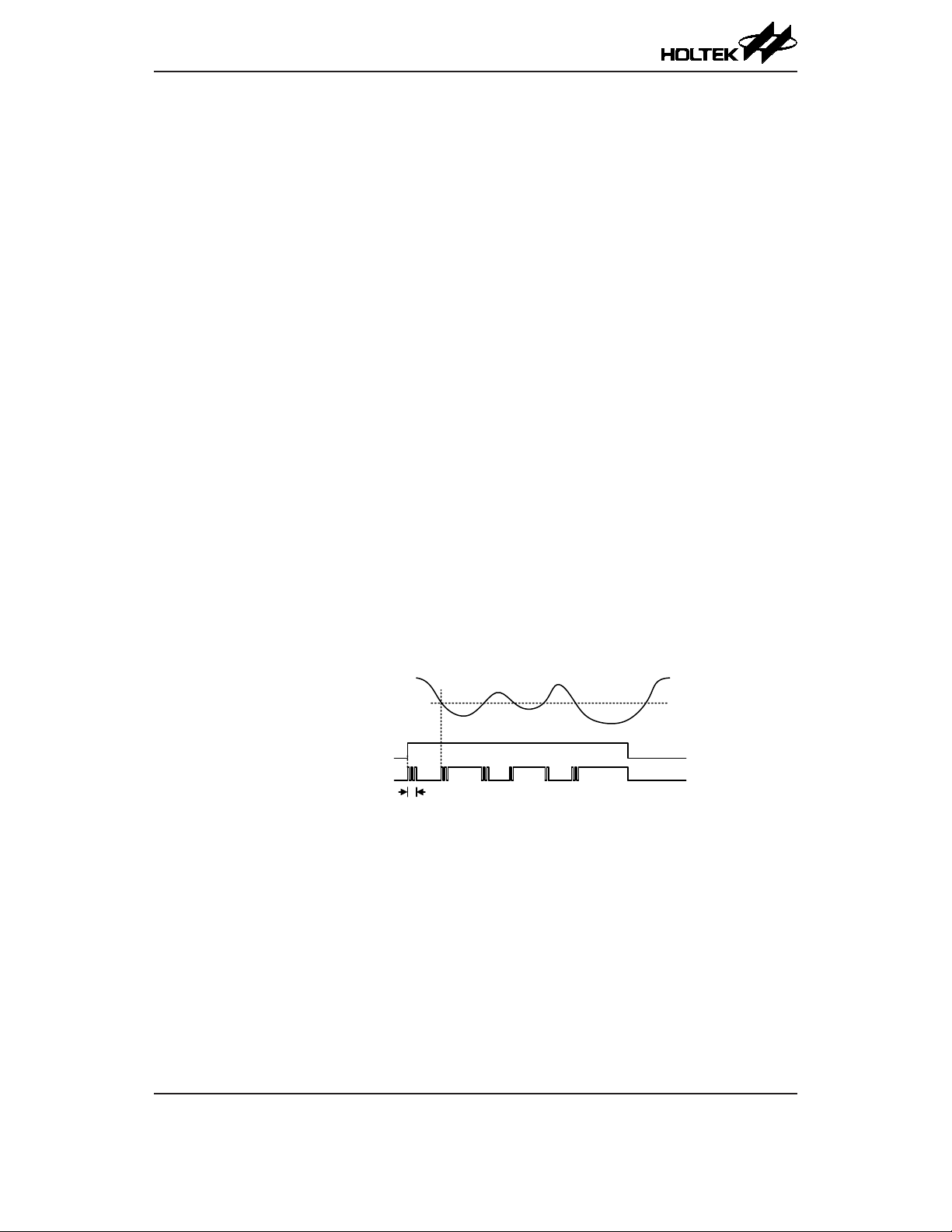
HT45F6530
AC Voltage Regulator Flash MCU
Bit 5 LVDO: LVD Output Flag
0: No Low Voltage Detect
1: Low Voltage Detect
Bit 4 LVDEN: Low Voltage Detector Control
0: Disable
1: Enable
Bit 3 VBGEN: Bandgap Buffer Control
0: Disable
1: Enable
Note that the Bandgap circuit is enabled when the LVD or LVR function is enabled or
when the VBGEN bit is set to 1.
Bit 2~0 VLVD2~VLVD0: Select LVD Voltage
000: 2.0V
001: 2.2V
010: 2.4V
011: 2.7V
100: 3.0V
101: 3.3V
110: 3.6V
111: 4.0V
LVD Operation
The Low Voltage Detector function operates by comparing the power supply voltage, VDD, with a
pre-specied voltage level stored in the LVDC register. This has a range of between 2.0V and 4.0V.
When the power supply voltage, VDD, falls below this pre-determined value, the LVDO bit will be
set high indicating a low power supply voltage condition. When the device is in the SLEEP mode,
the low voltage detector will be disabled even if the LVDEN bit is high. After enabling the Low
Voltage Detector, a time delay t
LVDO bit. Note also that as the VDD voltage may rise and fall rather slowly, at the voltage nears that
of V
, there may be multiple bit LVDO transitions.
LVD
should be allowed for the circuitry to stabilise before reading the
LVDS
V
DD
V
LVD
LVDEN
LVDO
t
LVDS
LVD Operation
The Low Voltage Detector also has its own interrupt, providing an alternative means of low voltage
detection, in addition to polling the LVDO bit. The interrupt will only be generated after a delay of
t
after the LVDO bit has been set high by a low voltage condition. In this case, the LVF interrupt
LVD
request flag will be set, causing an interrupt to be generated if VDD falls below the preset LVD
voltage. This will cause the device to wake-up from the IDLE Mode, however if the Low Voltage
Detector wake up function is not required then the LVF ag should be rst set high before the device
enter the IDLE Mode.
Page 90

Interrupts
Interrupts are an important part of any microcontroller system. When an external event or an
internal function such as a Timer Module or an A/D converter requires microcontroller attention,
their corresponding interrupt will enforce a temporary suspension of the main program allowing the
microcontroller to direct attention to their respective needs. The device contains several external
interrupt and internal interrupt functions. The external interrupts are generated by the action of the
external INT0~INT1 pins, while the internal interrupts are generated by various internal functions
such as the TMs, LVD and the A/D converter, etc.
Interrupt Registers
Overall interrupt control, which basically means the setting of request flags when certain
microcontroller conditions occur and the setting of interrupt enable bits by the application program,
is controlled by a series of registers, located in the Special Purpose Data Memory, as shown
in the accompanying table. The number of registers falls into three categories. The first is the
INTC0~INTC2 registers which setup the primary interrupts, the second is the MFI0~MFI1 registers
which setup the Multi-function interrupts. Finally there is an INTEG register to setup the external
interrupt trigger edge type.
Each register contains a number of enable bits to enable or disable individual registers as well as
interrupt flags to indicate the presence of an interrupt request. The naming convention of these
follows a specic pattern. First is listed an abbreviated interrupt type, then the (optional) number of
that interrupt followed by either an “E” for enable/disable bit or “F” for request ag.
AC Voltage Regulator Flash MCU
Function Enable Bit Request Flag Notes
Global EMI — —
Over Current
Protection
INTn Pin INTnE INTnF n=0~1
Multi-function MFnE MFnF n=0~1
Time Base TBnE TBnF n=0~1
A/D Converter ADE ADF —
EEPROM DEE DEF —
LVD LVE LVF —
TM
Interrupt Register Bit Naming Conventions
OCPnE OCPnF n=0~1
CTMnPE CTMnPF
CTMnAE CTMnAF
n=0~1
HT45F6530
Register
Name
INTEG — — — — INT1S1 INT1S0 INT0S1 INT0S0
INTC0 — INT0F OCP1F OCP0F INT0E OCP1E OCP0E EMI
INTC1 TB1F TB0F MF1F MF0F TB1E TB0E MF1E MF0E
INTC2 LVF INT1F DEF ADF LV E INT1E DEE ADE
MFI0 — — CTM0AF CTM0PF — — CTM0AE CTM0PE
MFI1 — — CTM1AF CTM1PF — — CTM1AE CTM1PE
Rev. 1.00 90 August 29, 2018 Rev. 1.00 91 August 29, 2018
7 6 5 4 3 2 1 0
Interrupt Register List
Bit
Page 91

HT45F6530
AC Voltage Regulator Flash MCU
• INTEG Register
Bit 7 6 5 4 3 2 1 0
Name — — — — INT1S1 INT1S0 INT0S1 INT0S0
R/W — — — — R/W R/W R/W R/W
POR — — — — 0 0 0 0
Bit 7~4 Unimplemented, read as “0”
Bit 3~2 INT1S1~INT1S0: Interrupt edge control for INT1 pin
00: Disable
01: Rising edge
10: Falling edge
11: Rising and falling edges
Bit 1~0 INT0S1~INT0S0: Interrupt edge control for INT0 pin
00: Disable
01: Rising edge
10: Falling edge
11: Rising and falling edges
• INTC0 Register
Bit 7 6 5 4 3 2 1 0
Name — INT0F OCP1F OCP0F INT0E OCP1E OCP0E EMI
R/W — R/W R/W R/W R/W R/W R/W R/W
POR — 0 0 0 0 0 0 0
Bit 7 Unimplemented, read as “0”
Bit 6 INT0F: INT0 interrupt request ag
0: No request
1: Interrupt request
Bit 5 OCP1F: Over Current Protection 1 interrupt request ag
0: No request
1: Interrupt request
Bit 4 OCP0F: Over Current Protection 0 interrupt request ag
0: No request
1: Interrupt request
Bit 3 INT0E: INT0 interrupt control
0: Disable
1: Enable
Bit 2 OCP1E: Over Current Protection 1 interrupt control
0: Disable
1: Enable
Bit 1 OCP0E: Over Current Protection 0 interrupt control
0: Disable
1: Enable
Bit 0 EMI: Global interrupt control
0: Disable
1: Enable
Page 92

HT45F6530
AC Voltage Regulator Flash MCU
• INTC1 Register
Bit 7 6 5 4 3 2 1 0
Name TB1F TB0F MF1F MF0F TB1E TB0E MF1E MF0E
R/W R/W R/W R/W R/W R/W R/W R/W R/W
POR 0 0 0 0 0 0 0 0
Bit 7 TB1F: Time Base 1 request ag
0: No request
1: Interrupt request
Bit 6 TB0F: Time Base 0 request ag
0: No request
1: Interrupt request
Bit 5 MF1F: Multi-function interrupt 1 request ag
0: No request
1: Interrupt request
Bit 4 MF0F: Multi-function interrupt 0 request ag
0: No request
1: Interrupt request
Bit 3 TB1E: Time Base 1 interrupt control
0: Disable
1: Enable
Bit 2 TB0E: Time Base 0 interrupt control
0: Disable
1: Enable
Bit 1 MF1E: Multi-function interrupt 1 control
0: Disable
1: Enable
Bit 0 MF0E: Multi-function interrupt 0 control
0: Disable
1: Enable
• INTC2 Register
Bit 7 6 5 4 3 2 1 0
Name LVF INT1F DEF ADF LVE INT1E DEE ADE
R/W R/W R/W R/W R/W R/W R/W R/W R/W
POR 0 0 0 0 0 0 0 0
Bit 7 LV F: LVD interrupt request ag
0: No request
1: Interrupt request
Bit 6 INT1F: INT1 interrupt request ag
0: No request
1: Interrupt request
Bit 5 DEF: Data EEPROM interrupt request ag
0: No request
1: Interrupt request
Bit 4 ADF: A/D Converter interrupt request ag
0: No request
1: Interrupt request
Bit 3 LV E: LVD interrupt control
0: Disable
1: Enable
Rev. 1.00 92 August 29, 2018 Rev. 1.00 93 August 29, 2018
Page 93

HT45F6530
AC Voltage Regulator Flash MCU
Bit 2 INT1E: INT1 interrupt control
0: Disable
1: Enable
Bit 1 DEE: Data EEPROM interrupt control
0: Disable
1: Enable
Bit 0 ADE: A/D Converter interrupt control
0: Disable
1: Enable
• MFI0 Register
Bit 7 6 5 4 3 2 1 0
Name — — CTM0AF CTM0PF — — CTM0AE CTM0PE
R/W — — R/W R/W — — R/W R/W
POR — — 0 0 — — 0 0
Bit 7~6 Unimplemented, read as “0”
Bit 5 CTM0AF: CTM0 Comparator A match interrupt request ag
0: No request
1: Interrupt request
Bit 4 CTM0PF: CTM0 Comparator P match interrupt request ag
0: No request
1: Interrupt request
Bit 3~2 Unimplemented, read as “0”
Bit 1 CTM0AE: CTM0 Comparator A match interrupt control
0: Disable
1: Enable
Bit 0 CTM0PE: CTM0 Comparator P match interrupt control
0: Disable
1: Enable
• MFI1 Register
Bit 7 6 5 4 3 2 1 0
Name — — CTM1AF CTM1PF — — CTM1AE CTM1PE
R/W — — R/W R/W — — R/W R/W
POR — — 0 0 — — 0 0
Bit 7~6 Unimplemented, read as “0”
Bit 5 CTM1AF: CTM1 Comparator A match interrupt request ag
0: No request
1: Interrupt request
Bit 4 CTM1PF: CTM1 Comparator P match interrupt request ag
0: No request
1: Interrupt request
Bit 3~2 Unimplemented, read as “0”
Bit 1 CTM1AE: CTM1 Comparator A match interrupt control
0: Disable
1: Enable
Bit 0 CTM1PE: CTM1 Comparator P match interrupt control
0: Disable
1: Enable
Page 94

Interrupt Operation
When the conditions for an interrupt event occur, such as a TM Comparator P or Comparator A
match or A/D conversion completion etc., the relevant interrupt request ag will be set. Whether
the request ag actually generates a program jump to the relevant interrupt vector is determined by
the condition of the interrupt enable bit. If the enable bit is set high then the program will jump to
its relevant vector; if the enable bit is zero then although the interrupt request ag is set an actual
interrupt will not be generated and the program will not jump to the relevant interrupt vector. The
global interrupt enable bit, if cleared to zero, will disable all interrupts.
When an interrupt is generated, the Program Counter, which stores the address of the next instruction
to be executed, will be transferred onto the stack. The Program Counter will then be loaded with a
new address which will be the value of the corresponding interrupt vector. The microcontroller will
then fetch its next instruction from this interrupt vector. The instruction at this vector will usually
be a “JMP” which will jump to another section of program which is known as the interrupt service
routine. Here is located the code to control the appropriate interrupt. The interrupt service routine
must be terminated with a “RETI”, which retrieves the original Program Counter address from
the stack and allows the microcontroller to continue with normal execution at the point where the
interrupt occurred.
The various interrupt enable bits, together with their associated request flags, are shown in the
accompanying diagrams with their order of priority. Some interrupt sources have their own
individual vector while others share the same multi-function interrupt vector. Once an interrupt
subroutine is serviced, all the other interrupts will be blocked, as the global interrupt enable bit,
EMI bit will be cleared automatically. This will prevent any further interrupt nesting from occurring.
However, if other interrupt requests occur during this interval, although the interrupt will not be
immediately serviced, the request ag will still be recorded.
If an interrupt requires immediate servicing while the program is already in another interrupt service
routine, the EMI bit should be set after entering the routine, to allow interrupt nesting. If the stack
is full, the interrupt request will not be acknowledged, even if the related interrupt is enabled, until
the Stack Pointer is decremented. If immediate service is desired, the stack must be prevented from
becoming full. In case of simultaneous requests, the accompanying diagram shows the priority that
is applied. All of the interrupt request ags when set will wake-up the device if it is in SLEEP or
IDLE Mode, however to prevent a wake-up from occurring the corresponding ag should be set
before the device is in SLEEP or IDLE Mode.
HT45F6530
AC Voltage Regulator Flash MCU
Rev. 1.00 94 August 29, 2018 Rev. 1.00 95 August 29, 2018
Page 95

HT45F6530
AC Voltage Regulator Flash MCU
Legend
xxF Request Flag, no auto reset in ISR
xxF Request Flag, auto reset in ISR
xxE Enable Bits
OCP0 Pin OCP0F OCP0E EMI
OCP1 Pin OCP1F OCP1E
Interrupt
Name
EMI auto disabled in ISR
Request
Flags
Enable
Bits
Master
Enable
EMI
Vector
04H
08H
Priority
High
Interrupt
Name
CTM0 Comp. P CTM0PF CTM0PE
CTM0 Comp. A CTM0AF CTM0AE
CTM1 Comp. P CTM1PF CTM1PE
CTM1 Comp. A CTM1AF CTM1AE
Request
Flags
Interrupts contained within
Multi-Function Interrupts
Enable
Bits
Over Current Protection Interrupts
An OCPn interrupt request will take place when the OCPn interrupt request flag, OCPnF, is set,
which occurs when the OCPn circuit detects a specic current condition. To allow the program to
branch to its respective interrupt vector address, the global interrupt enable bit, EMI, and OCPn
interrupt enable bit, OCPnE, must rst be set. When the interrupt is enabled, the stack is not full
and a user-dened current condition occurs, a subroutine call to the OCPn interrupt vector, will take
place. When the interrupt is serviced, the OCPn interrupt ag, OCPnF, will be automatically cleared.
The EMI bit will also be automatically cleared to disable other interrupts.
INT0 Pin INT0F INT0E
Multi-Function 0 MF0F MF0E
Multi-Function 1 MF1F MF1E
Time Base 0 TB0F TB0E
Time Base 1 TB1F TB1E
A/D Converter ADF ADE
EEPROM DEF DEE
INT1 INT1F INT1E
LVD LVF LVE
Interrupt Structure
EMI
EMI
EMI
EMI
EMI
EMI
EMI
EMI 28H
EMI
OCH
10H
14H
18H
1CH
20H
24H
2CH
Low
External Interrupts
The external interrupts are controlled by signal transitions on the pins INT0 and INT1. An external
interrupt request will take place when the external interrupt request ags, INT0F~INT1F, are set,
which will occur when a transition, whose type is chosen by the edge select bits, appears on the
external interrupt pins. To allow the program to branch to its respective interrupt vector address,
the global interrupt enable bit, EMI, and respective external interrupt enable bit, INT0E~INT1E,
must first be set. Additionally the correct interrupt edge type must be selected using the INTEG
register to enable the external interrupt function and to choose the trigger edge type. As the external
interrupt pins are pin-shared with I/O pins, they can only be congured as external interrupt pins if
their external interrupt enable bit in the corresponding interrupt register has been set and the external
interrupt pin is selected by the corresponding pin-shared function selection bits. The pin must also
be setup as an input by setting the corresponding bit in the port control register. When the interrupt
is enabled, the stack is not full and the correct transition type appears on the external interrupt pin,
a subroutine call to the external interrupt vector, will take place. When the interrupt is serviced, the
external interrupt request ags, INT0F~INT1F, will be automatically reset and the EMI bit will be
Page 96
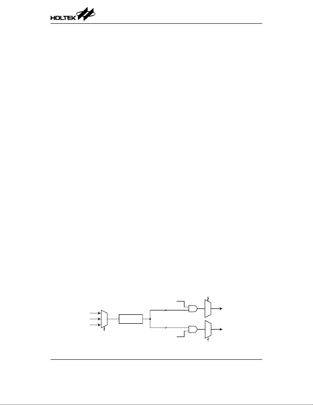
automatically cleared to disable other interrupts. Note that any pull-high resistor selections on the
external interrupt pins will remain valid even if the pin is used as an external interrupt input.
The INTEG register is used to select the type of active edge that will trigger the external interrupt.
A choice of either rising or falling or both edge types can be chosen to trigger an external interrupt.
Note that the INTEG register can also be used to disable the external interrupt function.
Multi-function Interrupts
Within the device there are up to two Multi-function interrupts. Unlike the other independent
interrupts, these interrupts have no independent source, but rather are formed from other existing
interrupt sources, namely the TM Interrupts.
A Multi-function interrupt request will take place when any of the Multi-function interrupt request
flags, MFnF are set. The Multi-function interrupt flags will be set when any of their included
functions generate an interrupt request ag. To allow the program to branch to its respective interrupt
vector address, the global interrupt enable bit, EMI, and the multi-function interrupt enable bit,
MFnE, must rst be set. When the Multi-function interrupt is enabled and the stack is not full, and
either one of the interrupts contained within each of Multi-function interrupt occurs, a subroutine
call to one of the Multi-function interrupt vectors will take place. When the interrupt is serviced, the
related Multi-function request ag will be automatically reset and the EMI bit will be automatically
cleared to disable other interrupts.
However, it must be noted that, although the Multi-function Interrupt ags will be automatically
reset when the interrupt is serviced, the request ags from the original source of the Multi-function
interrupts will not be automatically reset and must be manually reset by the application program.
HT45F6530
AC Voltage Regulator Flash MCU
Time Base Interrupts
The function of the Time Base Interrupts is to provide regular time signal in the form of an internal
interrupt. They are controlled by the overow signals from their respective timer functions. When
these happens their respective interrupt request flags, TB0F or TB1F will be set. To allow the
program to branch to their respective interrupt vector addresses, the global interrupt enable bit, EMI
and Time Base enable bits, TB0E or TB1E, must rst be set. When the interrupt is enabled, the stack
is not full and the Time Base overows, a subroutine call to their respective vector locations will
take place. When the interrupt is serviced, the respective interrupt request ag, TB0F or TB1F, will
be automatically reset and the EMI bit will be cleared to disable other interrupts.
The purpose of the Time Base Interrupt is to provide an interrupt signal at xed time periods. Its
clock source, f
through a divider, the division ratio of which is selected by programming the appropriate bits in the
TB0C and TB1C registers to obtain longer interrupt periods whose value ranges. The clock source
which in turn controls the Time Base interrupt period is selected using the CLKSEL1~CLKSEL0
bits in the PSCR register.
f
SYS
/4
f
SYS
f
SUB
PSC
M
U
X
CLKSEL[1:0]
, originates from the internal clock source f
TB0ON
f
/28~ f
PSC
f
PSC
Prescaler
f
/28~ f
PSC
Time Base Interrupts
PSC
PSC
TB1ON
15
/2
15
/2
SYS
, f
SYS
TB0[2:0]
M
U
X
M
U
X
TB1[2:0]
/4 or f
and then passes
SUB
Time Base 0 Interrupt
Time Base 1 Interrupt
Rev. 1.00 96 August 29, 2018 Rev. 1.00 97 August 29, 2018
Page 97
HT45F6530
AC Voltage Regulator Flash MCU
• PSCR Register
Bit 7 6 5 4 3 2 1 0
Name — — — — — — CLKSEL1 CLKSEL0
R/W — — — — — — R/W R/W
POR — — — — — — 0 0
Bit 7~2 Unimplemented, read as “0”
Bit 1~0 CLKSEL1~CLKSEL0: Prescaler clock source selection
00: f
SYS
01: f
/4
SYS
1x: f
SUB
• TB0C Register
Bit 7 6 5 4 3 2 1 0
Name TB0ON — — — — TB02 TB01 TB00
R/W R/W — — — — R/W R/W R/W
POR 0 — — — — 0 0 0
Bit 7 TB0ON: Time Base 0 Control
0: Disable
1: Enable
Bit 6~3 Unimplemented, read as “0”
Bit 2~0 TB02~TB00: Select Time Base 0 Time-out Period
000: 28/f
001: 29/f
010: 210/f
011: 211/f
100: 212/f
101: 213/f
110: 214/f
111: 215/f
PSC
PSC
PSC
PSC
PSC
PSC
PSC
PSC
• TB1C Register
Bit 7 6 5 4 3 2 1 0
Name TB1ON — — — — TB12 TB11 TB10
R/W R/W — — — — R/W R/W R/W
POR 0 — — — — 0 0 0
Bit 7 TB1ON: Time Base 1 Control
0: Disable
1: Enable
Bit 6~3 Unimplemented, read as “0”
Bit 2~0 TB12~TB10: Select Time Base 1 Time-out Period
000: 28/f
001: 29/f
010: 210/f
011: 211/f
100: 212/f
101: 213/f
110: 214/f
111: 215/f
PSC
PSC
PSC
PSC
PSC
PSC
PSC
PSC
Page 98

A/D Converter Interrupt
An A/D Converter Interrupt request will take place when the A/D Converter Interrupt request ag,
ADF, is set, which occurs when the A/D conversion process nishes. To allow the program to branch
to its respective interrupt vector address, the global interrupt enable bit, EMI, and A/D Interrupt
enable bit, ADE, must rst be set. When the interrupt is enabled, the stack is not full and the A/D
conversion process has ended, a subroutine call to the A/D Interrupt vector, will take place. When
the A/D Converter Interrupt is serviced, the A/D Interrupt ag, ADF, will be automatically cleared.
The EMI bit will also be automatically cleared to disable other interrupts.
EEPROM Interrupt
An EEPROM Interrupt request will take place when the EEPROM Interrupt request ag, DEF, is set,
which occurs when an EEPROM Write cycle ends. To allow the program to branch to its respective
interrupt vector address, the global interrupt enable bit, EMI, and EEPROM Interrupt enable bit,
DEE, must rst be set. When the interrupt is enabled, the stack is not full and an EEPROM Write
cycle ends, a subroutine call to the EEPROM Interrupt vector will take place. When the EEPROM
Interface Interrupt is serviced, the interrupt request ag, DEF, will be automatically reset and the
EMI bit will be cleared to disable other interrupts.
LVD Interrupt
An LVD Interrupt request will take place when the LVD Interrupt request ag, LVF, is set, which
occurs when the Low Voltage Detector function detects a low power supply voltage. To allow the
program to branch to its respective interrupt vector address, the global interrupt enable bit, EMI,
and Low Voltage Interrupt enable bit, LVE, must rst be set. When the interrupt is enabled, the stack
is not full and a low voltage condition occurs, a subroutine call to the LVD Interrupt vector, will
take place. When the LVD Interface Interrupt is serviced, the interrupt request ag, LVF, will be
automatically reset and the EMI bit will be cleared to disable other interrupts.
HT45F6530
AC Voltage Regulator Flash MCU
TM Interrupt
The Compact Type TM each have two interrupts, one comes from the comparator A match situation
and the other comes from the comparator P match situation. All of the TM interrupts are contained
within the Multi-function Interrupts. There are two interrupt request ags and two enable control
bits for each TM. A TM interrupt request will take place when any of the TM request ags are set, a
situation which occurs when a TM comparator P or A match situation happens.
To allow the program to branch to its respective interrupt vector address, the global interrupt enable
bit, EMI, respective TM Interrupt enable bit, and relevant Multi-function Interrupt enable bit, MFnE,
must rst be set. When the interrupt is enabled, the stack is not full and a TM comparator match
situation occurs, a subroutine call to the relevant Multi-function Interrupt vector locations, will take
place. When the TM interrupt is serviced, the EMI bit will be automatically cleared to disable other
interrupts, however only the related MFnF ag will be automatically cleared. As the TM interrupt
request ags will not be automatically cleared, they have to be cleared by the application program.
Rev. 1.00 98 August 29, 2018 Rev. 1.00 99 August 29, 2018
Page 99

HT45F6530
AC Voltage Regulator Flash MCU
Interrupt Wake-up Function
Each of the interrupt functions has the capability of waking up the microcontroller when in the
SLEEP or IDLE Mode. A wake-up is generated when an interrupt request ag changes from low
to high and is independent of whether the interrupt is enabled or not. Therefore, even though the
device is in the SLEEP or IDLE Mode and its system oscillator stopped, situations such as external
edge transitions on the external interrupt pins, a low power supply voltage or comparator output
bit change may cause their respective interrupt flag to be set high and consequently generate an
interrupt. Care must therefore be taken if spurious wake-up situations are to be avoided. If an
interrupt wake-up function is to be disabled then the corresponding interrupt request ag should be
set high before the device enters the SLEEP or IDLE Mode. The interrupt enable bits have no effect
on the interrupt wake-up function.
Programming Considerations
By disabling the relevant interrupt enable bits, a requested interrupt can be prevented from being
serviced, however, once an interrupt request flag is set, it will remain in this condition in the
interrupt register until the corresponding interrupt is serviced or until the request ag is cleared by
the application program.
Where a certain interrupt is contained within a Multi-function interrupt, then when the interrupt
service routine is executed, as only the Multi-function interrupt request flag, MFnF, will be
automatically cleared, the individual request flag for the function needs to be cleared by the
application program.
It is recommended that programs do not use the “CALL” instruction within the interrupt service
subroutine. Interrupts often occur in an unpredictable manner or need to be serviced immediately.
If only one stack is left and the interrupt is not well controlled, the original control sequence will be
damaged once a CALL subroutine is executed in the interrupt subroutine.
Every interrupt has the capability of waking up the microcontroller when it is in the SLEEP or IDLE
Mode, the wake up being generated when the interrupt request ag changes from low to high. If it is
required to prevent a certain interrupt from waking up the microcontroller then its respective request
ag should be rst set high before enter SLEEP or IDLE Mode.
As only the Program Counter is pushed onto the stack, then when the interrupt is serviced, if the
contents of the accumulator, status register or other registers are altered by the interrupt service
program, their contents should be saved to the memory at the beginning of the interrupt service
routine.
To return from an interrupt subroutine, either a RET or RETI instruction may be executed. The RETI
instruction in addition to executing a return to the main program also automatically sets the EMI
bit high to allow further interrupts. The RET instruction however only executes a return to the main
program leaving the EMI bit in its present zero state and therefore disabling the execution of further
interrupts.
Page 100

Application Description
Introduction
The main function of AVR products is to measure the input voltage, detect the AC zero-crossing
signal and then control a relay to switch the output voltage. Additional features include those for
protection against over-voltage, under-voltage and temperature. By including these functions, when
the AC input voltage is unstable, the relay will be switched to the internal multi-tap autotransformer
output voltage to continuously provide the backend loads with a stable voltage thus avoiding load
damage or shorter service life. Because there could be contact arcing during the internal relay
switching, it is necessary to control the relay timing to ensure it only switches during AC zero
crossing points to avoid relay damage. This Holtek AVR dedicated MCU provides full control
signals for all of the above functions, the details of which are described in the following sections.
Functional Description
AVR Input/Output Voltage Measurement Operating Principle
The D/A converter outputs a 2.5V bias voltage and the operational amplier together with external
resistors form an amplier circuit. By using these functions the AC waveform will be converted to a
sine wave with a 2.5V zero point. The peak-to-peak values can be obtained through continuous A/D
conversion during an AC cycle to convert the input/output voltage.
HT45F6530
AC Voltage Regulator Flash MCU
AVR Zero Crossing Detection Operating Principle
The AC input waveform conversion circuit is internally connected to a comparator where it is
compared with the D/A converter 2.5V output voltage. When this value is greater than 2.5V it will
output a high level. When it is lower than 2.5V a low level will be output and an interrupt generated.
AVR Relay Delay Measurement Operating Principle
The AC output waveform conversion circuit is internally connected to a comparator where it is
compared with the D/A converter output voltage. The relay will be turned on at the point where an
AC zero crossing and a rising edge both occur, therefore measure when the output voltage changes
and the time interval is the relay turn-on delay time. About 2~3ms before the AC zero crossing and
rising edge the relay is turned off, therefore measure when the output voltage changes from low to
high then low again, the time interval is the relay turn-off delay time.
Rev. 1.00 100 August 29, 2018 Rev. 1.00 101 August 29, 2018
 Loading...