

Page 1

A/D NFC Flash MCU
HT45F4050
Revision: V1.00 Date: September 11, 2018
Page 2

HT45F4050
A/D NFC Flash MCU
Table of Contents
Features ............................................................................................................ 7
CPU Features ......................................................................................................................... 7
Peripheral Features ................................................................................................................. 7
General Description ......................................................................................... 8
Block Diagram .................................................................................................. 9
Pin Assignment .............................................................................................. 10
Pin Description .............................................................................................. 10
Absolute Maximum Ratings .......................................................................... 15
D.C. Characteristics ....................................................................................... 15
A.C. Characteristics ....................................................................................... 18
Memory Characteristics ................................................................................ 20
A/D Converter Electrical Characteristics ..................................................... 21
Internal Reference Voltage Electrical Characteristics ................................ 22
LVD & LVR Electrical Characteristics .......................................................... 23
Comparator Electrical Characteristics ........................................................ 24
Software Controlled LCD Driver Electrical Characteristics ....................... 25
Power on Reset Characteristics ................................................................... 25
System Architecture ...................................................................................... 25
Clocking and Pipelining ......................................................................................................... 26
Program Counter ................................................................................................................... 26
Stack ..................................................................................................................................... 27
Arithmetic and Logic Unit – ALU ........................................................................................... 27
Flash Program Memory ................................................................................. 28
Structure ................................................................................................................................ 28
Special Vectors ..................................................................................................................... 28
Look-up Table ........................................................................................................................ 29
Table Program Example ........................................................................................................ 29
In Circuit Programming – ICP ............................................................................................... 30
On-Chip Debug Support – OCDS ......................................................................................... 31
Data Memory .................................................................................................. 31
Structure ................................................................................................................................ 32
Data Memory Addressing ...................................................................................................... 32
General Purpose Data Memory ............................................................................................ 32
Special Purpose Data Memory ............................................................................................. 33
Special Function Register Description ........................................................ 34
Indirect Addressing Registers – IAR0, IAR1, IAR2 ............................................................... 34
Memory Pointers – MP0, MP1L/MP1H, MP2L/MP2H ........................................................... 34
Accumulator – ACC ............................................................................................................... 36
Program Counter Low Register – PCL .................................................................................. 36
Rev. 1.00 2 September 11, 2018 Rev. 1.00 3 September 11, 2018
Page 3

HT45F4050
A/D NFC Flash MCU
Look-up Table Registers – TBLP, TBHP, TBLH ..................................................................... 36
Status Register – STATUS .................................................................................................... 36
EEPROM Data Memory .................................................................................. 38
EEPROM Data Memory Structure ........................................................................................ 38
EEPROM Registers .............................................................................................................. 38
Reading Data from the EEPROM ........................................................................................ 39
Writing Data to the EEPROM ................................................................................................ 40
Write Protection ..................................................................................................................... 40
EEPROM Interrupt ................................................................................................................ 40
Programming Considerations ................................................................................................ 41
Oscillators ...................................................................................................... 42
Oscillator Overview ............................................................................................................... 42
System Clock Congurations ............................................................................................... 42
External Crystal/Ceramic Oscillator – HXT ........................................................................... 43
Internal RC Oscillator – HIRC ............................................................................................... 44
External 32.768kHz Crystal Oscillator – LXT ........................................................................ 44
Internal 32kHz Oscillator – LIRC .......................................................................................... 45
Operating Modes and System Clocks ......................................................... 45
System Clocks ...................................................................................................................... 45
System Operation Modes ...................................................................................................... 46
Control Register .................................................................................................................... 47
Operating Mode Switching ................................................................................................... 50
Standby Current Considerations .......................................................................................... 54
Wake-up ................................................................................................................................ 54
Watchdog Timer ............................................................................................. 55
Watchdog Timer Clock Source .............................................................................................. 55
Watchdog Timer Control Register ......................................................................................... 55
Watchdog Timer Operation ................................................................................................... 56
Reset and Initialisation .................................................................................. 57
Reset Functions .................................................................................................................... 57
Reset Initial Conditions ........................................................................................................ 61
Input/Output Ports ........................................................................................ 65
Pull-high Resistors ................................................................................................................ 66
Port A Wake-up ..................................................................................................................... 66
I/O Port Control Registers ..................................................................................................... 67
I/O Port Source Current Control ............................................................................................ 67
I/O Port Power Source Control .............................................................................................. 69
Pin-shared Functions ............................................................................................................ 70
I/O Pin Structures .................................................................................................................. 77
Programming Considerations ............................................................................................... 77
Timer Modules – TM ...................................................................................... 78
Introduction ........................................................................................................................... 78
TM Operation ........................................................................................................................ 78
TM Clock Source ................................................................................................................... 78
Page 4

HT45F4050
A/D NFC Flash MCU
TM Interrupts ......................................................................................................................... 78
TM External Pins .................................................................................................................. 79
Programming Considerations ................................................................................................ 80
Compact Type TM – CTM .............................................................................. 81
Compact Type TM Operation ................................................................................................ 81
Compact Type TM Register Description................................................................................ 81
Compact Type TM Operating Modes .................................................................................... 85
Standard Type TM – STM .............................................................................. 91
Standard Type TM Operation ................................................................................................ 91
Standard Type TM Register Description ............................................................................... 91
Standard Type TM Operation Modes .................................................................................... 95
Periodic Type TM – PTM .............................................................................. 105
Periodic Type TM Operation................................................................................................ 105
Periodic Type TM Register Description ............................................................................... 105
Periodic Type TM Operation Modes .................................................................................... 109
Analog to Digital Converter – ADC ..............................................................118
A/D Converter Overview ......................................................................................................118
A/D Converter Register Description .....................................................................................119
A/D Converter Reference Voltage ....................................................................................... 122
A/D Converter Input Signals ................................................................................................ 123
A/D Converter Operation ..................................................................................................... 124
A/D Conversion Rate and Timing Diagram ......................................................................... 125
Summary of A/D Conversion Steps ..................................................................................... 126
Programming Considerations .............................................................................................. 127
A/D Conversion Function .................................................................................................... 127
A/D Converter Programming Examples .............................................................................. 128
Comparator .................................................................................................. 130
Comparator Operation ........................................................................................................ 130
Comparator Registers ......................................................................................................... 130
Input Offset Calibration ...................................................................................................... 132
Serial Interface Module – SIM ..................................................................... 133
SPI Interface ....................................................................................................................... 133
I2C Interface ........................................................................................................................ 142
UART Interface ............................................................................................. 152
UART External Pins ............................................................................................................ 153
UART Data Transfer Scheme.............................................................................................. 153
UART Status and Control Registers.................................................................................... 153
Baud Rate Generator .......................................................................................................... 159
UART Setup and Control..................................................................................................... 160
UART Transmitter................................................................................................................ 161
UART Receiver ................................................................................................................... 162
Managing Receiver Errors .................................................................................................. 164
UART Interrupt Structure..................................................................................................... 165
UART Power Down and Wake-up ....................................................................................... 166
Rev. 1.00 4 September 11, 2018 Rev. 1.00 5 September 11, 2018
Page 5

HT45F4050
A/D NFC Flash MCU
Near Field Communication – NFC .............................................................. 167
NFC Power Management .................................................................................................... 167
NFC Memory ....................................................................................................................... 168
NFC Control Registers ....................................................................................................... 171
Collisions between the MCU and NFC RF Interface ........................................................... 178
NFC State Diagram and Logical Status Descriptions ......................................................... 179
NFC Command Set ............................................................................................................. 181
SCOM Controlled LCD Driver ..................................................................... 189
LCD Operation .................................................................................................................... 189
LCD Bias Current Control ................................................................................................... 190
Interrupts ...................................................................................................... 191
Interrupt Registers ............................................................................................................... 191
Interrupt Operation .............................................................................................................. 196
External Interrupts ............................................................................................................... 197
Comparator Interrupt ........................................................................................................... 198
Multi-function Interrupts ....................................................................................................... 198
A/D Converter Interrupt ....................................................................................................... 198
Time Base Interrupts ........................................................................................................... 198
Serial Interface Module Interrupt ......................................................................................... 200
UART Transfer Interrupt ...................................................................................................... 200
NFC Interrupt ...................................................................................................................... 201
EEPROM Write Interrupt ..................................................................................................... 201
LVD Interrupt ....................................................................................................................... 201
TM Interrupts ...................................................................................................................... 201
Interrupt Wake-up Function ................................................................................................. 202
Programming Considerations .............................................................................................. 202
Low Voltage Detector – LVD ....................................................................... 203
LVD Register ....................................................................................................................... 203
LVD Operation ..................................................................................................................... 204
Conguration Options ................................................................................. 205
Application Descriptions ............................................................................ 206
NFC Operating Principle ..................................................................................................... 206
Hardware Block Diagram .................................................................................................... 206
Hardware Circuit ................................................................................................................. 208
Instruction Set .............................................................................................. 209
Introduction ......................................................................................................................... 209
Instruction Timing ................................................................................................................ 209
Moving and Transferring Data ............................................................................................. 209
Arithmetic Operations .......................................................................................................... 209
Logical and Rotate Operation ............................................................................................. 210
Branches and Control Transfer ........................................................................................... 210
Bit Operations ..................................................................................................................... 210
Table Read Operations ....................................................................................................... 210
Other Operations ................................................................................................................. 210
Page 6

HT45F4050
A/D NFC Flash MCU
Instruction Set Summary .............................................................................211
Table Conventions ................................................................................................................211
Extended Instruction Set ..................................................................................................... 213
Instruction Denition ................................................................................... 215
Extended Instruction Denition ........................................................................................... 224
Package Information ................................................................................... 231
48-pin LQFP (7mm × 7mm) Outline Dimensions ................................................................ 232
Rev. 1.00 6 September 11, 2018 Rev. 1.00 7 September 11, 2018
Page 7

HT45F4050
A/D NFC Flash MCU
Features
CPU Features
• Operating Voltage
♦
f
=4MHz: 1.8V~5.5V
SYS
♦
f
=8MHz: 2.0V~5.5V
SYS
♦
f
=12MHz: 2.7V~5.5V
SYS
♦
f
=16MHz: 3.3V~5.5V
SYS
• Up to 0.25μs instruction cycle with 16MHz system clock at VDD=5V
• Power down and wake-up functions to reduce power consumption
• Oscillator types
♦
External High Speed Crystal – HXT
♦
Internal High Speed RC – HIRC
♦
External Low Speed 32.768kHz Crystal – LXT
♦
Internal Low Speed 32kHz RC – LIRC
• Multi-mode operation: NORMAL, SLOW, IDLE and SLEEP
• Fully integrated internal oscillators require no external components
• All instructions executed in one to three instruction cycles
• Table read instructions
• 115 powerful instructions
• 8-level subroutine nesting
• Bit manipulation instruction
Peripheral Features
• Flash Program Memory: 8K×16
• RAM Data Memory: 256×8
• True EEPROM Memory: 64×8
• Watchdog Timer function
• 41 bidirectional I/O lines
• I/O source current programmable
• Software controlled 4-SCOM lines LCD driver with 1/2 bias
• Two external interrupt lines shared with I/O pins
• Multiple Timer Modules for time measure, input capture, compare match output, PWM output or
single pulse output functions
• Serial Interfaces Module – SIM for SPI or I2C
• Single Fully-duplex Universal Asynchronous Receiver and Transmitter Interface – UART
• Dual Time-Base functions for generation of xed time interrupt signals
• One comparator function
• 13 external channels 12-bit resolution A/D converter
Page 8

• NFC AFE (can only be tuned under VDD=2.2V~5.5V)
♦
Standards: NFC Forum Type 2 and ISO14443 Type A
♦
Demodulation: 100% ASK
♦
RF data rate: 106 kbit/s
♦
LDO supply power (1.8V) for 100% ASK demodulator and NFC clock recovery
♦
NFC EEPROM: 256 bytes
♦
NFC SRAM: 64 bytes
• Low Voltage Reset function
• Low Voltage Detect function
• Package type: 48-pin LQFP
General Description
The device is an Flash Memory type 8-bit high performance RISC architecture microcontroller
especially designed fro Near Field Communication, NFC, applications. Offering users the
convenience of Flash Memory multi-programming features, the device also includes a wide range of
functions and features. Other memory includes an area of RAM Data Memory as well as an area of
true EEPROM memory for storage of non-volatile data such as serial numbers, calibration data etc,
however the unique feature of this device is its fully integrated NFC circuitry.
Analog features include a multi-channel 12-bit A/D converter and a comparator function. Multiple
and extremely flexible Timer Modules provide timing, pulse generation and PWM generation
functions. Communication with the outside world is catered for by including fully integrated SPI,
I2C and UART interface functions, popular interfaces which provide designers with a means of easy
communication with external peripheral hardware. Protective features such as an internal Watchdog
Timer, Low Voltage Reset and Low Voltage Detector coupled with excellent noise immunity and
ESD protection ensure that reliable operation is maintained in hostile electrical environments.
A full choice of external and internal, high speed and low speed oscillator functions are provided
including a fully integrated system oscillator which requires no external components for its
implementation. The ability to operate and switch dynamically between a range of operating modes
using different clock sources gives users the ability to optimise microcontroller operation and
minimize power consumption.
The device includes a new NFC Forum compliant Type 2 tag product based on NFC-A technology
for the 13.56MHz contactless IC card standards and for the ISO/IEC14443 Type A specications.
Being compliant with the ISO/IEC14443A Reader/Writer Passive communication mode, the device
can be accessed by other NFC devices with an extremely short connection time with the advantage
of extra-low power consumption.
The inclusion of flexible I/O programming features, timebase functions along with many other
features ensure that the device will nd excellent use in applications such as smart meters, smart
appliances, NFC data loggers in addition to many others.
HT45F4050
A/D NFC Flash MCU
Rev. 1.00 8 September 11, 2018 Rev. 1.00 9 September 11, 2018
Page 9

HT45F4050
A/D NFC Flash MCU
Block Diagram
Pin-Shared
With Port B
OSC1
OSC2
XT1
XT2
Pin-Shared
With Port B
Pin-Shared
With Port F
Reset
Circuit
Interrupt
Controller
Time Bases
Limiter
ASK 100%
Demodulator
Modulator
Clock Recovery
: SIM including SPI & I2C
INT0~INT1
VDDIO V
VDD
AVDD
VSS
AVSS
LA
LB
VSSN
: Pin-Shared Node
RES
Pin-Shared
With Port A
DDIO
V
DD
AV
DD
V
SS
AV
SS
ROM
8K × 16
EEPROM
64 × 8
Watchdog
Timer
SYSCLK
4/8/12MHz
NFC Peripheral
HT8 MCU Core
LIRC
32kHz
HIRC
HXT
LXT
Clock System
Field
Detector
NFC State Machine
NFC Memory
RAM
256 × 8
Stack
8-level
LVD/LVR
MUX
V
DD
Regulator
Bus
SIM
UART
Timers
SCOM
I/O
Digital Peripherals
PGA
AV
DD
12-bit
ADC
MUX
Analog to Digital Converter
Comparator
CMP
Analog Peripherals
Pin-Shared
Function
V
BGREF
Port A
Driver
Port B
Driver
Port C
Driver
Port D
Driver
Port E
Driver
Port F
Driver
Pin-Shared
With Port C
PA0~PA7
PB0~PB7
PC0~PC7
PD0~PD3
PE0~PE4
PF0~PF7
VREFI
AV
DD
AVDD/2
AVDD/4
V
R
VR/2
V
/4
R
+
-
Pin-Shared
With Port C/D/F
VREF
AN0~
AN12
C+
C-
Pin-Shared With Port F
CX
Pin-Shared With Port B
Page 10
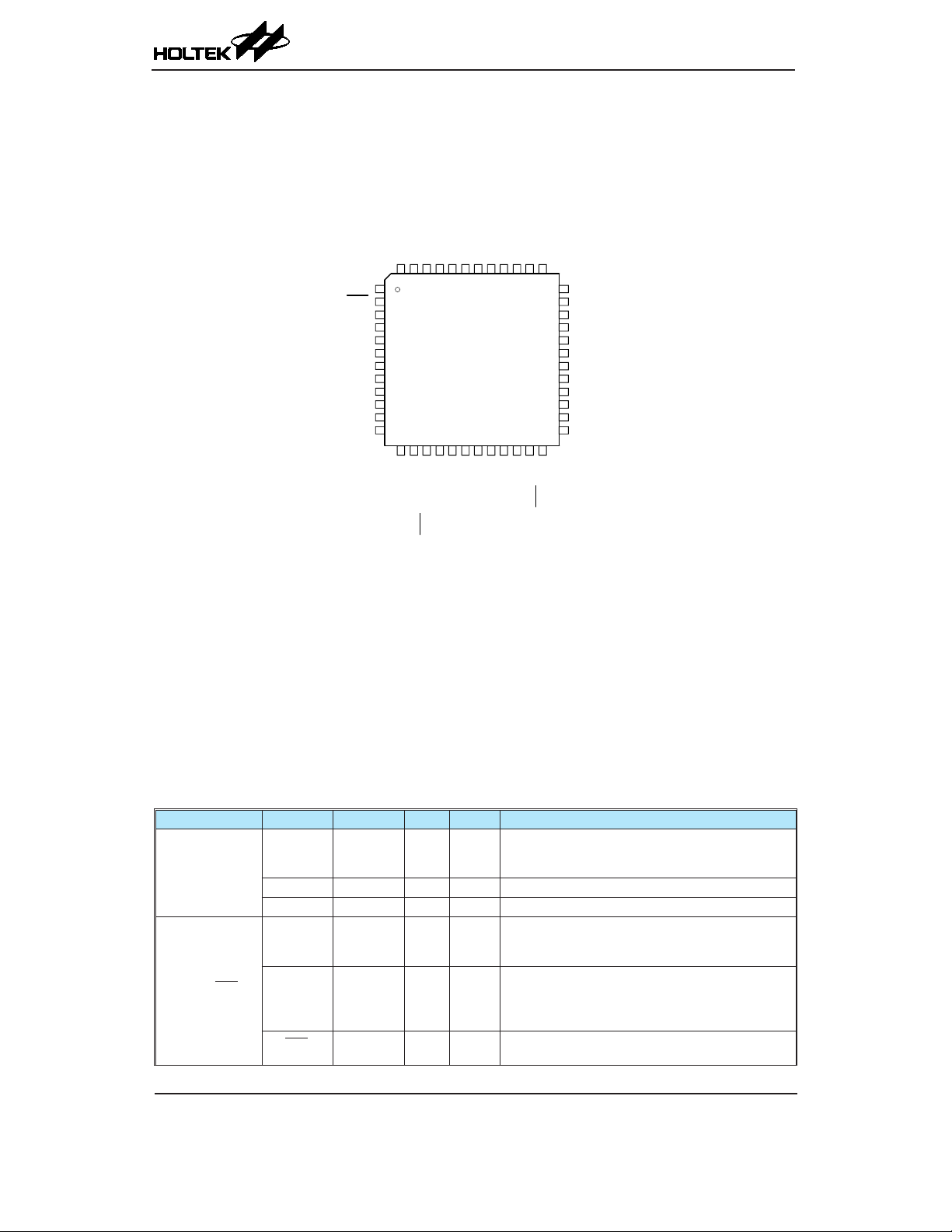
Pin Assignment
PA0/ICPDA/OCDSDA
PA2/ICPCK/OCDSCK
PB4/CTCK/CTPB
PB5/RES
VSSN
LB
LA
VSS
VDD
PB6/OSC1
PB7/OSC2
PE0/STCK/STPB
PB2/PTCK/PTPB
PB1/PTPI/PTP
PF6/AN12/C-
PD2/AN10
PD3/AN11
PD0/AN8
PA7/INT1/TX
PA6/INT0/RX
PE3/VDDIO/CTP
PD1/AN9
PE4
PE2/CTCK/CTPB
PB3/CTP
PB0/CX
PF7/C+
45
464748 3738394041424344
1
2
3
4
5
HT45F4050/HT45V4050
6
7
8
9
10
11
12
48 LQFP-A
13 14 15 16 17 18 19 20 21 22 23 24
PA3/INT1/SDO
PE1/STPI/STP
PA4/SDI/SDA
PA5/SCK/SCL
PA1/INT0/SCS
PC7/STCK/STPB/AN7
PC6/STPI/STP/AN6
PC5/AN5
36
35
PC4/AN4
PC3/PTCK/PTPB/AN3
34
PC2/PTPI/PTP/AN2
33
PC1/AN1/CX/VREF
32
31
PC0/AN0/VREFI
30
AVSS
29
PF5/XT1
28
PF4/XT2
27
AVDD
PF3/SCK/SCL/SCOM3
26
25
PF2/SDI/SDA/SCOM2
PF0/SCS/SCOM0
PF1/SDO/SCOM1
HT45F4050
A/D NFC Flash MCU
Notes: 1. If the pin-shared pin functions have multiple outputs simultaneously, the desired pin-shared function is
determined by the corresponding software control bits.
2. The actual device and its equivalent OCDS EV device share the same package type, however the OCDS
EV device part number is HT45V4050. Pins OCDSCK and OCDSDA which are pin-shared with PA2
and PA0 are only used for the OCDS EV device.
Pin Description
With the exception of the power pins, all pins on the device can be referenced by its Port name,
e.g. PA0, PA1 etc., which refer to the digital I/O function of the pins. However these Port pins are
also shared with other function such as the Analog to Digital Converter, Timer Module pins etc.
The function of each pin is listed in the following table, however the details behind how each pin is
congured is contained in other sections of the datasheet.
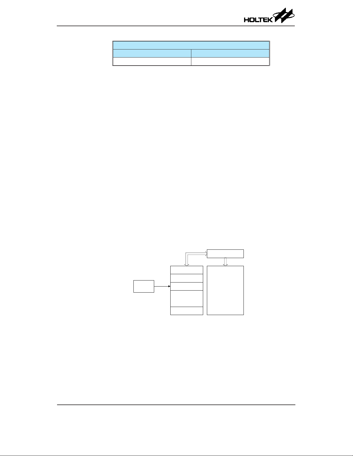
Pin Name Function OPT I/T O/T Description
PA0/ICPDA/
OCDSDA
PA1/INT0/SCS
PA0
PAWU
ST CMOS
PAS0
ICPDA — ST CMOS ICP Address/Data pin
OCDSDA — ST CMOS OCDS Address/Data pin, for EV chip only
PAPU
PAPU
PA1
PAWU
ST CMOS
PAS0
PAS0
INT0
INTEG
INTC0
ST — External Interrupt 0
IFS1
SCS
PAS0
IFS0
ST CMOS SPI slave select
General purpose I/O. Register enabled pull-high and
wake-up.
General purpose I/O. Register enabled pull-high and
wake-up.
Rev. 1.00 10 September 11, 2018 Rev. 1.00 11 September 11, 2018
Page 11
HT45F4050
A/D NFC Flash MCU
Pin Name Function OPT I/T O/T Description
PA2/ICPCK/
OCDSCK
PA3/INT1/SDO
PA4/SDI/SDA
PA5/SCK/SCL
PA6/INT0/RX
PA7/INT1/TX
PB0/CX
PB1/PTPI/PTP
PA2
ICPCK — ST — ICP Clock pin
OCDSCK — ST — OCDS Clock pin, for EV chip only
PA3
INT1
SDO PAS0 — CMOS SPI data output
PA4
SDI
SDA
PA5
SCK
SCL
PA6
INT0
RX PAS1 ST — UART RX serial data input
PA7
INT1
TX PAS1 — CMOS UART TX serial data output
PB0
CX PBS0 — CMOS Comparator output
PB1
PTPI
PTP PBS0 — CMOS PTM output
PAPU
PAWU
PAS0
PAPU
PAWU
PAS0
PAS0
INTEG
INTC2
IFS1
PAPU
PAWU
PAS1
PAS1
IFS0
PAS1
IFS0
PAPU
PAWU
PAS1
PAS1
IFS0
PAS1
IFS0
PAPU
PAWU
PAS1
PAS 1
INTEG
INTC0
IFS1
PAPU
PAWU
PAS1
PAS 1
INTEG
INTC2
IFS1
PBPU
PBS0
PBPU
PBS0
PBS0
IFS0
ST CMOS
ST CMOS
ST — External Interrupt 1
ST CMOS
ST — SPI data input
ST NMOS I2C data line
ST CMOS
ST CMOS SPI serial Clock
ST NMOS I2C clock line
ST CMOS
ST — External Interrupt 0
ST CMOS
ST — External Interrupt 1
ST CMOS General purpose I/O. Register enabled pull-high.
ST CMOS General purpose I/O. Register enabled pull-high.
ST — PTM capture input
General purpose I/O. Register enabled pull-high and
wake-up.
General purpose I/O. Register enabled pull-high and
wake-up.
General purpose I/O. Register enabled pull-high and
wake-up.
General purpose I/O. Register enabled pull-high and
wake-up.
General purpose I/O. Register enabled pull-high and
wake-up.
General purpose I/O. Register enabled pull-high and
wake-up.
Page 12

A/D NFC Flash MCU
Pin Name Function OPT I/T O/T Description
PBPU
PBS0
PBS0
IFS0
PBPU
PBS0
PBPU
PBS1
PBS1
IFS0
PBPU
PBS1
RSTC
PBS1
RSTC
PBPU
PBS1
PBPU
PBS1
PCPU
PCS0
PCPU
PCS0
PCPU
PCS0
PCS0
IFS0
PCPU
PCS0
PCS0
IFS0
PCPU
PCS1
PCPU
PCS1
ST CMOS General purpose I/O. Register enabled pull-high.
ST — PTM clock input
ST CMOS General purpose I/O. Register enabled pull-high.
ST CMOS General purpose I/O. Register enabled pull-high.
ST — CTM clock input
ST CMOS General purpose I/O. Register enabled pull-high.
ST — External reset input
ST CMOS General purpose I/O. Register enabled pull-high.
ST CMOS General purpose I/O. Register enabled pull-high.
ST CMOS General purpose I/O. Register enabled pull-high.
ST CMOS General purpose I/O. Register enabled pull-high.
ST CMOS General purpose I/O. Register enabled pull-high.
ST — PTM capture input
ST CMOS General purpose I/O. Register enabled pull-high.
ST — PTM clock input
ST CMOS General purpose I/O. Register enabled pull-high.
ST CMOS General purpose I/O. Register enabled pull-high.
PB2/PTCK/PTPB
PB3/CTP
PB4/CTCK/CTPB
PB5/RES
PB6/OSC1
PB7/OSC2
PC0/AN0/VREFI
PC1/AN1/CX/
VREF
PC2/PTPI/PTP/
AN2
PC3/PTCK/
PTPB/AN3
PC4/AN4
PC5/AN5
PB2
PTCK
PTPB PBS0 — CMOS PTM inverted output
PB3
CTP PBS0 — CMOS CTM output
PB4
CTCK
CTPB PBS1 — CMOS CTM inverted output
PB5
RES
PB6
OSC1 PBS1 HXT — HXT oscillator pin
PB7
OSC2 PBS1 — HXT HXT oscillator pin
PC0
AN0 PCS0 AN — A/D Converter analog input
VREFI PCS0 AN — A/D Converter PGA input
PC1
AN1 PCS0 AN — A/D Converter analog input
CX PCS0 — CMOS Comparator output
VREF PCS0 AN — A/D Converter reference voltage input
PC2
PTPI
PTP PCS0 — CMOS PTM output
AN2 PCS0 AN — A/D Converter analog input
PC3
PTCK
PTPB PCS0 — CMOS PTM inverted output
AN3 PCS0 AN — A/D Converter analog input
PC4
AN4 PCS1 AN — A/D Converter analog input
PC5
AN5 PCS1 AN — A/D Converter analog input
HT45F4050
Rev. 1.00 12 September 11, 2018 Rev. 1.00 13 September 11, 2018
Page 13

HT45F4050
A/D NFC Flash MCU
Pin Name Function OPT I/T O/T Description
PC6
PC6/STPI/STP/
AN6
PC7/STCK/
STPB/AN7
PD0/AN8
PD1/AN9
PD2/AN10
PD3/AN11
PE0/STCK/STPB
PE1/STPI/STP
PE2/CTCK/CTPB
PE3/VDDIO/CTP
PE4 PE4
PF0/SES/SCOM0
STPI
STP PCS1 — CMOS STM output
AN6 PCS1 AN — A/D Converter analog input
PC7
STCK
STPB PCS1 — CMOS STM inverted output
AN7 PCS1 AN — A/D Converter analog input
PD0
AN8 PDS0 AN — A/D Converter analog input
PD1
AN9 PDS0 AN — A/D Converter analog input
PD2
AN10 PDS0 AN — A/D Converter analog input
PD3
AN11 PDS0 AN — A/D Converter analog input
PE0
STCK
STPB PES0 — CMOS STM inverted output
PE1
STPI
STP PES0 — CMOS STM output
PE2
CTCK
CTPB PES0 — CMOS CTM inverted output
PE3
VDDIO PES0 PWR — SPI/I2C/UART pin power supply
CTP PES0 ST — CTM clock input
PF0
SES
SCOM0 PFS0 — SCOM Software controlled LCD COM output
PCPU
PCS1
PCS1
IFS0
PCPU
PCS1
PCS1
IFS0
PDPU
PDS0
PDPU
PDS0
PDPU
PDS0
PDPU
PDS0
PEPU
PES0
PES0
IFS0
PEPU
PES0
PES0
IFS0
PEPU
PES0
PES0
IFS0
PEPU
PES0
PEPU
PES1
PFPU
PFS0
PFS0
IFS0
ST CMOS General purpose I/O. Register enabled pull-high.
ST — STM capture input
ST CMOS General purpose I/O. Register enabled pull-high.
ST — STM clock input
ST CMOS General purpose I/O. Register enabled pull-high.
ST CMOS General purpose I/O. Register enabled pull-high.
ST CMOS General purpose I/O. Register enabled pull-high.
ST CMOS General purpose I/O. Register enabled pull-high.
ST CMOS General purpose I/O. Register enabled pull-high.
ST — STM clock input
ST CMOS General purpose I/O. Register enabled pull-high.
ST — STM capture input
ST CMOS General purpose I/O. Register enabled pull-high.
ST — CTM clock input
ST CMOS General purpose I/O. Register enabled pull-high.
ST CMOS General purpose I/O. Register enabled pull-high.
ST CMOS General purpose I/O. Register enabled pull-high.
ST CMOS SPI slave select
Page 14

A/D NFC Flash MCU
Pin Name Function OPT I/T O/T Description
PF1/SDO/
SCOM1
PF2/SDI/SDA/
SCOM2
PF3/SCK/SCL/
SCOM3
PF4/XT2
PF5/XT1
PF6/AN12/C-
PF7/C+
LA LA — AN AN Antenna connection LA
LB LB — AN AN Antenna connection LB
VDD VDD — PWR — Positive power supply
AVDD AVDD — PWR — Analog positive power supply
VSS VSS — PWR — Negative power supply, ground
AVSS AVSS — PWR — Analog negative power supply, ground
VSSN VSSN — PWR — NFC AFE negative power supply
PF1
SDO PFS0 — CMOS SPI data output
SCOM1 PFS0 — SCOM Software controlled LCD COM output
PF2
SDI
SDA
SCOM2 PFS0 — SCOM Software controlled LCD COM output
PF3
SCK
SCL
SCOM3 PFS0 — SCOM Software controlled LCD COM output
PF4
XT2 PFS1 — LXT LXT oscillator pin
PF5
XT1 PFS1 LXT — LXT oscillator pin
PF6
AN12 PFS1 AN — A/D Converter analog input
C- PFS1 AN — Comparator negative input
PF7
C+ PFS1 AN — Comparator positive input
Legend: I/T: Input type; O/T: Output type;
OPT: Optional by register option; PWR: Power
ST: Schmitt Trigger input; AN: Analog signal;
CMOS: CMOS output; NMOS: NMOS output;
SCOM: Software controlled LCD COM;
HXT: High frequency crystal oscillator;
LXT: Low frequency crystal oscillator.
PFPU
PFS0
PFPU
PFS0
PFS0
IFS0
PFS0
IFS0
PFPU
PFS0
PFS0
IFS0
PFS0
IFS0
PFPU
PFS1
PFPU
PFS1
PFPU
PFS1
PFPU
PFS1
ST CMOS General purpose I/O. Register enabled pull-high.
ST CMOS General purpose I/O. Register enabled pull-high.
ST — SPI data input
ST NMOS I2C data line
ST CMOS General purpose I/O. Register enabled pull-high.
ST CMOS SPI serial Clock
ST NMOS I2C clock line
ST CMOS General purpose I/O. Register enabled pull-high.
ST CMOS General purpose I/O. Register enabled pull-high.
ST CMOS General purpose I/O. Register enabled pull-high.
ST CMOS General purpose I/O. Register enabled pull-high.
HT45F4050
Rev. 1.00 14 September 11, 2018 Rev. 1.00 15 September 11, 2018
Page 15
HT45F4050
A/D NFC Flash MCU
Absolute Maximum Ratings
Supply Voltage ................................................................................................VSS−0.3V to VSS+6.0V
Input Voltage ..................................................................................................VSS−0.3V to VDD+0.3V
Storage Temperature ....................................................................................................-50˚C to 125˚C
Operating Temperature ..................................................................................................-40˚C to 85˚C
IOH Total .................................................................................................................................... -80mA
IOL Total ..................................................................................................................................... 80mA
Total Power Dissipation .........................................................................................................500mW
Note: These are stress ratings only. Stresses exceeding the range specified under "Absolute
Maximum Ratings" may cause substantial damage to the device. Functional operation of this
device at other conditions beyond those listed in the specication is not implied and prolonged
exposure to extreme conditions may affect device reliability.
D.C. Characteristics
Symbol Parameter
Operating Voltage (HXT) —
V
DD
Operating Voltage (HIRC) —
Operating Voltage (LXT) — f
Operating Voltage (LIRC) — f
V
DDIO
I
DD
VDDIO Pin Power Supply — — 1.8 — V
Operating Current (HXT)
V
3V
5V — 1.3 1.8
3V No load, all peripherals off,
5V — 2.3 3.2
3V
5V — 2.6 3.2
3V No load, all peripherals off,
5V — 3.3 4.7
3V
5V — 2.7 3.9
3V No load, all peripherals off,
5V — 4.7 6.7
5V
5V
Test Conditions
DD
f
SYS=fHXT
f
SYS=fHXT
f
SYS=fHXT
f
SYS=fHXT
f
SYS=fHIRC
SYS=fHIRC
f
SYS=fHIRC
SYS=fLXT
SYS=fLIRC
Conditions
=4MHz 1.8 — 5.5
=8MHz 2.0 — 5.5
=12MHz 2.7 — 5.5
=16MHz 3.3 — 5.5
=4MHz 1.8 — 5.5
=8MHz 2.0 — 5.5
=12MHz 2.7 — 5.5
=32.768kHz 1.8 — 5.5 V
=32kHz 1.8 — 5.5 V
No load, all peripherals off,
f
=4MHz
SYS=fHXT
f
=4MHz,
SYS=fHXT
NFC communication is in progress
No load, all peripherals off,
f
=8MHz
SYS=fHXT
f
=8MHz,
SYS=fHXT
NFC communication is in progress
No load, all peripherals off,
f
=12MHz
SYS=fHXT
f
=12MHz,
SYS=fHXT
NFC communication is in progress
No load, all peripherals off,
f
=16MHz
SYS=fHXT
No load, all peripherals off,
f
=16MHz,
SYS=fHXT
NFC communication is in progress
Ta=-40°C~85°C, unless otherwise specied
Min. Typ. Max. Unit
V
Vf
V
DD
— 0.8 1.1
— 1.2 1.7
— 1.1 1.5
— 1.7 2.3
— 1.5 2.1
mA
— 2.3 3.2
— 3.3 4.8
— 5.7 8.2
Page 16

HT45F4050
A/D NFC Flash MCU
Symbol Parameter
Operating Current (HIRC)
I
DD
Operating Current (LXT)
Operating Current (LIRC)
Operating Current,
fH=8MHz (HIRC)
Operating Current,
fH=12MHz (HXT)
Standby Current
(SLEEP mode)
Standby Current
(IDLE0 mode)
Standby Current
I
STB
(IDLE1 mode, HIRC)
Standby Current
(IDLE1 mode, HXT)
Test Conditions
V
DD
3V
No load, all peripherals off,
f
SYS=fHIRC
5V — 1.3 1.8
No load, all peripherals off,
3V
f
SYS=fHIRC
5V — 2.3 3.2
NFC communication is in progress
3V
No load, all peripherals off,
f
SYS=fHIRC
5V — 2.6 3.2
No load, all peripherals off,
3V
f
SYS=fHIRC
5V — 3.3 4.7
NFC communication is in progress
3V
No load, all peripherals off,
f
SYS=fHIRC
5V — 2.7 3.9
No load, all peripherals off,
3V
f
SYS=fHIRC
5V — 4.7 6.7
NFC communication is in progress
3V
No load, all peripherals off,
f
SYS=fLXT
5V — 30 50
3V
No load, all peripherals off,
f
SYS=fLIRC
5V — 30 50
3V
No load, all peripherals off, f
5V — 1.0 2.0
3V
No load, all peripherals off,
f
SYS=fH
5V — 0.5 1.0
3V
No load, all peripherals off, f
5V — 1.4 2.8
3V
No load, all peripherals off,
f
SYS=fH
5V — 0.7 1.4
3V
No load, all peripherals off,
WDT off
5V — 0.5 1.0
3V
No load, all peripherals off,
WDT on
5V — — 5
3V
No load, all peripherals off,
f
on
SUB
5V — 5 10
3V
No load, all peripherals off,
f
on, f
SUB
5V — 0.5 1.0
3V
No load, all peripherals off,
f
on, f
SUB
5V — 1.0 2.0
3V
No load, all peripherals off,
f
on, f
SUB
5V — 1.4 2.8
3V
No load, all peripherals off,
f
on, f
SUB
5V — 0.5 1.0
3V
No load, all peripherals off,
f
on, f
SUB
5V — 1.0 2.0
3V
No load, all peripherals off,
f
on, f
SUB
5V — 1.5 3.0
No load, all peripherals off,
5V
f
on, f
SUB
Conditions
=4MHz
=4MHz,
=8MHz
=8MHz,
=12MHz
=12MHz,
=32768Hz
=32kHz
/64
/64
SYS=fHIRC
SYS=fHIRC
SYS=fHIRC
SYS=fHXT
SYS=fHXT
SYS=fHXT
SYS=fHXT
SYS=fH
SYS=fH
=4MHz
=8MHz
=12MHz
=4MHz
=8MHz
=12MHz
=16MHz
Min. Typ. Max. Unit
— 0.8 1.1
— 1.2 1.7
— 1.1 1.5
— 1.7 2.3
— 1.5 2.1
— 2.3 3.2
— 10 20
— 10 20
— 0.5 1.0
/2
— 0.25 0.5
— 0.7 1.4
/2
— 0.35 0.7
— 0.2 0.8
— — 3
— 3 5
— 0.25 0.5
— 0.5 1.0
— 0.7 1.4
— 0.25 0.5
— 0.5 1.0
— 0.7 1.4
— 2.0 4.0
mA
μA
μA
mA
mA
μA
μA
mA
mA
Rev. 1.00 16 September 11, 2018 Rev. 1.00 17 September 11, 2018
Page 17

HT45F4050
A/D NFC Flash MCU
Symbol Parameter
Input Low Voltage for I/O
Ports
V
IL
Input Low Voltage for PA1,
PA3~PA7 Pins
Input Low Voltage for RES
Pin
Input High Voltage for I/O
Ports
V
IH
Input High Voltage for PA1,
PA3~PA7 Pins
Input High Voltage for RES
Pin
I
OL
I
OH
R
PH
Sink Current for I/O Ports
Source Current for I/O Ports
Pull-high Resistance for I/O
Ports
Test Conditions
V
DD
5V
— 0 — 0.2V
5V PMPS[1:0]=10B or 11B, V
Conditions
—
DDIO=VDD
Min. Typ. Max. Unit
0 — 1.5
0 — 1.5
— PMPS[1:0]=10B or 11B 0 — 0.2V
— — 0 — 0.4V
5V
— 0.8V
5V PMPS[1:0]=10B or 11B, V
—
DDIO=VDD
— PMPS[1:0]=10B or 11B 0.8V
— — 0.9V
1.8V
VOL=0.1V
3V 16 32 —
DD
3.5 — 5.0
— V
DD
3.5 — 5.0
— V
DDIO
— V
DD
7 14 —
5V 32 64 —
1.8V
VOL=0.1V
3V 16 32 —
DDIO
, V
DDIO=VDD
7 14 —
5V 32 64 —
3V
VOH=0.9VDD, SLEDCn[m+1, m]=00B
(n=0, 1 or 2, m=0, 2, 4 or 6)
5V -2.0 -4.0 —
3V VOH=0.9V
SLEDCn[m+1, m]=00B
5V -2.0 -4.0 —
(n=0, 1 or 2, m=0, 2, 4 or 6)
3V
VOH=0.9VDD, SLEDCn[m+1, m]=01B
(n=0, 1 or 2, m=0, 2 or, or 6)
5V -3.5 -7.0 —
3V VOH=0.9V
SLEDCn[m+1, m]=01B
5V -3.5 -7.0 —
(n=0, 1 or 2, m=0, 2, 4 or 6)
3V
VOH=0.9VDD, SLEDCn[m+1, m]=10B
(n=0, 1 or 2, m=0, 2, 4 or 6)
5V -5.0 -10 —
3V VOH=0.9V
SLEDCn[m+1, m]=10B
5V -5.0 -10 —
(n=0, 1 or 2, m=0, 2, 4 or 6)
3V
VOH=0.9VDD, SLEDCn[m+1, m]=11B
(n=0, 1 or 2, m=0, 2, 4 or 6)
5V -11 -22 —
3V VOH=0.9V
SLEDCn[m+1, m]=11B
5V -11 -22 —
(n=0, 1 or 2, m=0, 2, 4 or 6)
3V
LVPU=0
5V 10 30 50
3V
LVPU=0, V
5V 10 30 50
3V
LVPU=1
5V 3.5 7.5 12
3V
LVPU=1, V
5V 3.5 7.5 12
, V
DDIO
, V
DDIO
, V
DDIO
, V
DDIO
DDIO=VDD
DDIO=VDD
DDIO=VDD
DDIO=VDD
DDIO=VDD
DDIO=VDD
,
,
,
,
-1.0 -2.0 —
-1.0 -2.0 —
-1.75 -3.5 —
-1.75 -3.5 —
-2.5 -5.0 —
-2.5 -5.0 —
-5.5 -11 —
-5.5 -11 —
20 60 100
20 60 100
6.67 15 23
6.67 15 23
DD
V
DDIO
DD
DD
V
DDIO
DD
mA
mA
kΩ
Page 18
HT45F4050
A/D NFC Flash MCU
Symbol Parameter
NFC Function
V
LDO
I
OUT
I
Q
LDO Output Voltage
LDO Output Current
LDO Quiescent Current
A.C. Characteristics
Symbol Parameter
System Clock (HXT)
f
SYS
System Clock (HIRC)
System Clock (LXT) 1.8V~5.5V f
System Clock (LIRC) 1.8V~5.5V f
High Speed Internal RC Oscillator
(HIRC=4MHz,
trim 4MHz @ VDD=3V)
f
HIRC
High Speed Internal RC Oscillator
(HIRC=4MHz,
trim 4MHz @ VDD=5V )
Test Conditions
V
DD
Conditions
Min. Typ. Max. Unit
2.2V
I
=700μA, Ta=-40°C~85°C 1.71 1.80 1.89 V3V
LOAD
5V
2.2V
3V
ΔV
=-3%, Ta=-40°C~85°C 200 ─ ─ μA
LDO
5V
2.2V
No load, Ta=-40°C~85°C ─ ─ 20 μA3V
5V
Ta=-40°C~85°C, unless otherwise specied
Test Conditions
V
DD
1.8V~5.5V f
2.0V~5.5V f
2.7V~5.5V f
3.3V~5.5V f
1.8V~5.5V f
2.7V~5.5V f
Conditions
=4MHz — 4 —
SYS=fHXT
=8MHz — 8 —
SYS=fHXT
=12MHz — 12 —
SYS=fHXT
=16MHz — 16 —
SYS=fHXT
=4MHz — 4 —
SYS=fHIRC
=8MHz — 8 —
SYS=fHIRC
=12MHz — 12 —
SYS=fHIRC
=32.768kHz — 32.768 — kHz
SYS=fLXT
=32kHz — 32 — kHz
SYS=fLIRC
Min. Typ. Max. Unit
3.0V Ta=25°C -2% 4 +2%
2.2V~5.5V Ta=25°C -5% 4 +5%
3.0V Ta=0°C~70°C -5% 4 +5%
3.0V Ta=-40°C~85°C -5% 4 +5%
2.2V~5.5V Ta=0°C~70°C -7% 4 +7%
2.2V~5.5V Ta=-40°C~85°C -10% 4 +10%
3.0V Ta=25°C -20% 8 +20%
3.0V Ta=25°C -20% 12 +20%
5.0V Ta=25°C -2% 4 +2%
2.2V~5.5V Ta=25°C -5% 4 +5%
5.0V Ta=0°C~70°C -5% 4 +5%
5.0V Ta=-40°C~85°C -5% 4 +5%
2.2V~5.5V Ta=0°C~70°C -7% 4 +7%
2.2V~5.5V Ta=-40°C~85°C -10% 4 +10%
5.0V Ta=25°C -20% 8 +20%
5.0V Ta=25°C -20% 12 +20%
MHz
MHz2.0V~5.5V f
MHz
MHz
Rev. 1.00 18 September 11, 2018 Rev. 1.00 19 September 11, 2018
Page 19

HT45F4050
A/D NFC Flash MCU
Symbol Parameter
High Speed Internal RC Oscillator
(HIRC=8MHz,
trim 8MHz @ VDD=3V)
High Speed Internal RC Oscillator
f
HIRC
(HIRC=8MHz,
trim 8MHz @ VDD=5V)
High Speed Internal RC Oscillator
(HIRC=12MHz,
trim 12MHz @ VDD=5V)
f
LIRC
t
TCK
t
TPI
t
INT
t
SRESET
Low Speed Internal RC Oscillator
(LIRC)
CTCK, STCK and PTCK Pin
Minimum Pulse Width
STPI, PTPI Pin Minimum Pulse
Width
External Interrupt Minimum Pulse
Width
Minimum Software Reset Width
to Reset
System Reset Delay Time (Reset
source from Power-on reset or
LVR hardware reset)
t
RSTD
System Reset Delay Time (LVRC/
WDTC/RSTC software reset)
System Reset Delay Time (Reset
source from WDT overow or
RES pin reset)
Test Conditions
V
DD
Conditions
Min. Typ. Max. Unit
3.0V Ta=25°C -2% 8 +2%
3.0V~5.5V Ta=25°C -5% 8 +5%
3.0V Ta=0°C~70°C -5% 8 +5%
3.0V Ta=-40°C~85°C -5% 8 +5%
3.0V~5.5V Ta=0°C~70°C -7% 8 +7%
3.0V~5.5V Ta=-40°C~85°C -10% 8 +10%
3.0V Ta=25°C -20% 4 +20%
3.0V Ta=25°C -20% 12 +20%
5.0V Ta=25°C -2% 8 +2%
3.0V~5.5V Ta=25°C -5% 8 +5%
5.0V Ta=0°C~70°C -5% 8 +5%
5.0V Ta=-40°C~85°C -5% 8 +5%
3.0V~5.5V Ta=0°C~70°C -7% 8 +7%
3.0V~5.5V Ta=-40°C~85°C -10% 8 +10%
5.0V Ta=25°C -20% 4 +20%
5.0V Ta=25°C -20% 12 +20%
5.0V Ta=25°C -2% 12 +2%
4.0V~5.5V Ta=25°C -5% 12 +5%
5.0V Ta=0°C~70°C -5% 12 +5%
5.0V Ta=-40°C~85°C -5% 12 +5%
4.0V~5.5V Ta=0°C~70°C -7% 12 +7%
4.0V~5.5V Ta=-40°C~85°C -10% 12 +10%
5.0V Ta=25°C -20% 4 +20%
5.0V Ta=25°C -20% 8 +20%
2.2V~5.5V
Ta=25°C -5% 32 +5%
Ta=-40°C~85°C -10% 32 +10%
— — 0.3 — — μs
— — 0.3 — — μs
— — 10 — — μs
— — 45 90 120 μs
— RR
POR
=5V/ms
42 48 54 ms
— —
— — 14 16 18 ms
MHz
MHz
MHz
kHz
Page 20

HT45F4050
A/D NFC Flash MCU
Symbol Parameter
System Start-up Timer Period
(Wake-up from Power Down
Mode and f
SYS
Off)
System Start-up Timer Period
(Slow Mode ↔ Normal Mode, or
t
SST
fH=f
HIRC
↔ f
HXT
, or f
SUB=fLIRC
↔ f
System Start-up Timer Period
(Wake-up from Power Down
Mode and f
SYS
On)
System Start-up Timer Period
(WDT Time-out Hardware Cold
Reset)
NFC Function
f
PLL
t
SETUP
t
RCY
t
WCY
Note: t
NFC PLL Frequency 2.2V~5.5V Ta=-40°C~85°C -7% 13.56 +7% MHz
NFC PLL Setup Time 2.2V~5.5V Ta=-40°C~85°C — — 90 μs
NFC EEPROM Read Time 2.2V~5.5V Ta=-40°C~85°C — — 200 t
NFC EEPROM Write Time 2.2V~5.5V Ta=-40°C~85°C — 4 6 ms
=1/f
SYS
SYS
Memory Characteristics
Symbol Parameter
V
RW
Flash Program / Data EEPROM Memory
t
DEW
t
DER
I
DDPGM
E
P
t
RETD
RAM Data Memory
V
DR
VDD for Read / Write — — V
Erase / Write Time – Flash Program
Memory
Write Cycle Time – Data EEPROM
Memory
Read Time – Flash Program Memory /
Data EEPROM Memory
Programming / Erase current on V
Cell Endurance — — 100K — — E/W
ROM Data Retention time — Ta=25°C — 40 — Year
RAM Data Retention voltage — Device in SLEEP Mode 1.0 — — V
LXT
Test Conditions
V
DD
— f
— f
— f
— f
— f
— f
)
— f
—
— f
Conditions
SYS=fSUB=fLXT
~ fH/64, fH=f
SYS=fH
~ fH/64, fH=f
SYS=fH
SYS=fSUB=fLIRC
off → on (HXTF=1) — 1024 — t
HXT
off → on (HIRCF=1) — 16 — t
HIRC
off → on (LXTF=1) — 1024 — t
LXT
f
~ fH/64,
SYS=fH
f
or f
SYS=fHXT
or f
SYS=fLXT
HXT
HIRC
HIRC
LIRC
Min. Typ. Max. Unit
— 1024 — t
— 128 — t
— 16 — t
— 2 — t
— 2 — t
— 2 — t
— — — 0 — t
Ta=-40°C~85°C, unless otherwise specied
Test Conditions
V
DD
Conditions
Min. Typ. Max. Unit
DDmin
— — — 2 3 ms
— — — 4 6 ms
— — — — 4 t
— — — — 5.0 mA
DD
— V
DDmax
LXT
HXT
HIRC
LIRC
HXT
HIRC
LXT
H
SUB
H
SYS
V
SYS
Rev. 1.00 20 September 11, 2018 Rev. 1.00 21 September 11, 2018
Page 21

HT45F4050
A/D NFC Flash MCU
A/D Converter Electrical Characteristics
Symbol Parameter
AV
V
V
Operating Voltage — — 1.8 — 5.5 V
DD
Input Voltage — — 0 — V
ADI
Reference Voltage — — 1.8 — AV
REF
DNL Differential Nonlinearity
INL Integral Nonlinearity
I
ADC
t
ADCK
t
ON2ST
t
ADS
Additional Current for A/D
Converter Enable
Clock Period —
A/D Converter On-to-Start
Time
Sampling Time — — — 4 — t
Conversion Time
t
ADC
(Include A/D Sample and
Hold Time)
I
PGA
V
Additional Current for PGA
Enable
PGA Input Voltage Range
IR
V
DD
1.8V
2V
3V
5V
1.8V
3V
5V
1.8V
2V
3V
5V
1.8V
3V
5V
1.8V No load (t
5V No load (t
— — 4 — — μs
— — — 16 — t
2.2V
5V — 400 550
3V
5V VSS+0.1 — VDD-1.4
Test Conditions
Conditions
SAINS[3:0]=0000B, SAVRS[1:0]=01B,
V
REF=VDD
, t
ADCK
SAINS[3:0]=0000B, SAVRS[1:0]=01B,
V
REF=VDD
, t
ADCK
SAINS[3:0]=0000B, SAVRS[1:0]=01B,
V
REF=VDD
, t
ADCK
SAINS[3:0]=0000B, SAVRS[1:0]=01B,
V
REF=VDD
, t
ADCK
SAINS[3:0]=0000B, SAVRS[1:0]=01B,
V
REF=VDD
, t
ADCK
SAINS[3:0]=0000B, SAVRS[1:0]=01B,
V
REF=VDD
, t
ADCK
SAINS[3:0]=0000B, SAVRS[1:0]=01B,
V
REF=VDD
, t
ADCK
SAINS[3:0]=0000B, SAVRS[1:0]=01B,
V
REF=VDD
, t
ADCK
SAINS[3:0]=0000B, SAVRS[1:0]=01B,
V
REF=VDD
, t
ADCK
SAINS[3:0]=0000B, SAVRS[1:0]=01B,
V
REF=VDD
, t
ADCK
SAINS[3:0]=0000B, SAVRS[1:0]=01B,
V
REF=VDD
, t
ADCK
SAINS[3:0]=0000B, SAVRS[1:0]=01B,
V
REF=VDD
, t
ADCK
SAINS[3:0]=0000B, SAVRS[1:0]=01B,
V
REF=VDD
, t
ADCK
SAINS[3:0]=0000B, SAVRS[1:0]=01B,
V
1.8V ≤ V
2.0V ≤ V
REF=VDD
, t
ADCK
ADCK
ADCK
ADCK
< 2.0V 2.0 — 10
DD
≤ 5.5V 0.5 — 10
DD
No load
Gain=1, PGAIS=0, Relative gain,
Gain error < ±5%
VDD=AVDD, Ta=-40°C~85°C, unless otherwise specied
Min. Typ. Max. Unit
V
REF
V
DD
=2.0μs
=0.5μs
=0.5μs
=0.5μs
-3 — +3 LSB
=10μs
=10μs
=10μs
=2.0μs
=0.5μs
=0.5μs
=0.5μs
-4 — +4 LSB
=10μs
=10μs
=10μs
=2.0μs) — 0.5 1.0
=0.5μs) — 1.0 2.0
mA3V No load (t
=0.5μs) — 1.5 3.0
μs
ADCK
ADCK
— 250 400
μA3V — 300 450
VSS+0.1 — VDD-1.4
V
Page 22

HT45F4050
A/D NFC Flash MCU
Symbol Parameter
V
PGA Maximum Output
OR
Voltage Range
V
DD
2.2V
Test Conditions
Conditions
—
Min. Typ. Max. Unit
VSS+0.1 — VDD-0.1
5V VSS+0.1 — VDD-0.1
2.2V~
Ta=-40°C~85°C,
5.5V
VRI=V
3.2V~
V
Fix Voltage Output of PGA
VR
5.5V
4.2V~
5.5V
Ta=-40°C~85°C,
VRI=V
Ta=-40°C~85°C,
VRI=V
(PGAIS=1)
BGREF
(PGAIS=1)
BGREF
(PGAIS=1)
BGREF
-1% 2 +1%
-1% 3 +1%
-1% 4 +1%
Internal Reference Voltage Electrical Characteristics
Ta=-40°C~85°C, unless otherwise specied
Symbol Parameter
V
V
I
BGREF
Operating Voltage — — 2.2 — 5.5 V
DD
Bandgap Reference Voltage — Ta= -40°C~85°C -2% 1.2 +2% V
BGREF
Operating Current 5.5V Ta=-40°C~85°C — 25 40 μA
PSRR Power Supply Rejection Ratio —
En Output Noise —
I
SD
t
START
Shutdown Current — VBGREN=0 — — 0.1 μA
Startup Time 2.2V~5.5V — — — 400 μs
Note: 1. All the above parameters are measured under conditions of no load condition unless otherwise decribed.
2. A 0.1μF ceramic capacitor should be connected between VDD and GND.
3. The V
voltage is used as the A/D converter PGA input.
BGREF
V
DD
Test Conditions
Conditions
V
=1V
RIPPLE
f
RIPPLE
P-P
=100Hz
,
no load current,
f=0.1Hz ~ 10Hz
Min. Typ. Max. Unit
75 — — dB
— 300 — μV
V3V VSS+0.1 — VDD-0.1
V
RMS
Rev. 1.00 22 September 11, 2018 Rev. 1.00 23 September 11, 2018
Page 23

HT45F4050
A/D NFC Flash MCU
LVD & LVR Electrical Characteristics
Symbol Parameter
V
LVR
V
LVD
I
LVRLVDBG
t
LVDS
t
LVR
t
LVD
I
LVR
I
LVD
Low Voltage Reset Voltage
Low Voltage Detection
Voltage
Operating Current
LVDO Stable Time
Minimum Low Voltage Width
to Reset
Minimum Low Voltage Width
to Interrupt
Additional Current for LVR
Enable
Additional Current for LVD
Enable
V
DD
— LVR enable, voltage select 1.65V -5% 1.7 +5%
— LVR enable, voltage select 1.9V -5% 1.9 +5%
— LVR enable, voltage select 2.55V -3% 2.55 +3%
— LVR enable, voltage select 3.15V -3% 3.15 +3%
— LVR enable, voltage select 3.8V -3% 3.8 +3%
— LVD enable, voltage select 1.8V -5% 1.8 +5%
— LVD enable, voltage select 2.0V -5% 2.0 +5%
— LVD enable, voltage select 2.4V -5% 2.4 +5%
— LVD enable, voltage select 2.7V -5% 2.7 +5%
— LVD enable, voltage select 3.0V -5% 3.0 +5%
— LVD enable, voltage select 3.3V -5% 3.3 +5%
— LVD enable, voltage select 3.6V -5% 3.6 +5%
— LVD enable, voltage select 4.0V -5% 4.0 +5%
3V
5V — 8 15
— For LVR enable, LVD off → on — — 15
— For LVR disable, LVD off → on — — 150
— — 120 240 480 μs
— — 60 120 240 μs
5V LVD disable — — 8 μA
5V LVR disable — — 8 μA
Test Conditions
LVD enable, LVR enable,
V
=1.9V, V
LVR
Conditions
=2V
LVD
Ta=-40°C~85°C, unless otherwise specied
Min. Typ. Max. Unit
V
V
— — 10
μA
μs
Page 24

HT45F4050
A/D NFC Flash MCU
Comparator Electrical Characteristics
Ta=-40°C~85°C, unless otherwise specied
Symbol Parameter
V
DD
Operating Voltage — — 1.8 — 5.5 V
V
1.8V
3V — 1 5
5V — 1 5
1.8V
3V — 14 30
I
CMP
Additional Current for Comparator
Enable
5V — 14 30
1.8V
3V — 36 65
5V — 36 65
1.8V
3V — 58 110
5V — 58 110
1.8V
3V -10 — 10
V
OS
Input Offset Voltage
5V -10 — 10
1.8V
3V -4 — 4
5V -4 — 4
1.8V
V
CM
Common Mode Voltage Range
5V V
1.8V
A
OL
Open Loop Gain
5V 60 80 —
1.8V
V
HYS
Hysteresis
5V 10 24 30
1.8V
3V — — 40 μs
5V — — 40 μs
1.8V
3V — — 3 μs
t
RP
Response Time
(2)
5V — — 3 μs
1.8V
3V — — 1.5 μs
5V — — 1.5 μs
1.8V
3V — — 1 μs
5V — — 1 μs
Note: 1. The input offset voltage should rst be calibrated when the comparator operates with the compared threshold
voltage level lower than 250mV. Otherwise, the input offset voltage will be out of specication.
2. Load condition: C
LOAD
=50pF
3. All measurement is under C+ input voltage=(VDD-1.4)/2 and remain constant.
Test Conditions
DD
Conditions
CNVT[1:0]=00B
CNVT[1:0]=01B
CNVT[1:0]=10B
CNVT[1:0]=11B
Without calibration
(COF[4:0]=10000B),
CNVT[1:0]=00B
With calibration,
CNVT[1:0]=00B
CNVT[1:0]=00B
CNVT[1:0]=00B
With 100mV overdrive,
C
=50pF, CNVT[1:0]=00B
LOAD
With 100mV overdrive,
C
=50pF, CNVT[1:0]=01B
LOAD
With 100mV overdrive,
C
=50pF, CNVT[1:0]=10B
LOAD
With 100mV overdrive,
C
=50pF, CNVT[1:0]=11B
LOAD
Min. Typ. Max. Unit
— 1 5
— 14 30
— 36 65
μA
— 58 110
-10 — 10
-4 — 4
(1)
V
0.3 — VDD-1.0
SS+
—
SS
SS
— VDD-1.0
— VDD-1.0
mV
V3V V
60 — —
dB3V 60 — —
10 — 30
mV3V 10 — 30
— — 40 μs
— — 3 μs
— — 1.5 μs
— — 1 μs
Rev. 1.00 24 September 11, 2018 Rev. 1.00 25 September 11, 2018
Page 25

HT45F4050
A/D NFC Flash MCU
Software Controlled LCD Driver Electrical Characteristics
Ta=-40°C~85°C, unless otherwise specied
Symbol Parameter
I
V
BIAS
SCOM
VDD/2 Bias Current for LCD
VDD/2 Voltage for LCD COM Port 2.2V~5.5V No load 0.475VDD0.5VDD0.525VDDV
Test Conditions
V
DD
3V
5V 17.5 25 32.5
3V
5V 35 50 65
3V
5V 70 100 130
3V
5V 140 200 260
Conditions
ISEL[1:0]=00B
ISEL[1:0]=01B
ISEL[1:0]=10B
ISEL[1:0]=11B
Min. Typ. Max. Unit
10.5 15 19.5
21 30 39
42 60 78
82.6 118 153.4
Power on Reset Characteristics
Ta=-40°C~85°C, unless otherwise specied
Symbol Parameter
V
RR
t
POR
POR
POR
VDD Start Voltage to Ensure Power-on Reset — — — — 100 mV
VDD Rising Rate to Ensure Power-on Reset — — 0.035 — — V/ms
Minimum Time for VDD Stays at V
Power-on Reset
to Ensure
POR
Test Conditions
V
DD
Conditions
Min. Typ. Max. Unit
— — 1 — — ms
μA
System Architecture
A key factor in the high-performance features of the Holtek range of microcontrollers is attributed to
their internal system architecture. The range of the device take advantage of the usual features found
within RISC microcontrollers providing increased speed of operation and enhanced performance.
The pipelining scheme is implemented in such a way that instruction fetching and instruction
execution are overlapped, hence instructions are effectively executed in one or two cycles for most
of the standard or extended instructions respectively. The exceptions to this are branch or call
instructions which need one more cycle. An 8-bit wide ALU is used in practically all instruction set
operations, which carries out arithmetic operations, logic operations, rotation, increment, decrement,
branch decisions, etc. The internal data path is simplied by moving data through the Accumulator
and the ALU. Certain internal registers are implemented in the Data Memory and can be directly
or indirectly addressed. The simple addressing methods of these registers along with additional
architectural features ensure that a minimum of external components is required to provide a
functional I/O and A/D control system with maximum reliability and flexibility. This makes the
device suitable for low-cost, high-volume production for controller applications.
V
DD
t
POR
RR
POR
V
POR
Time
Page 26
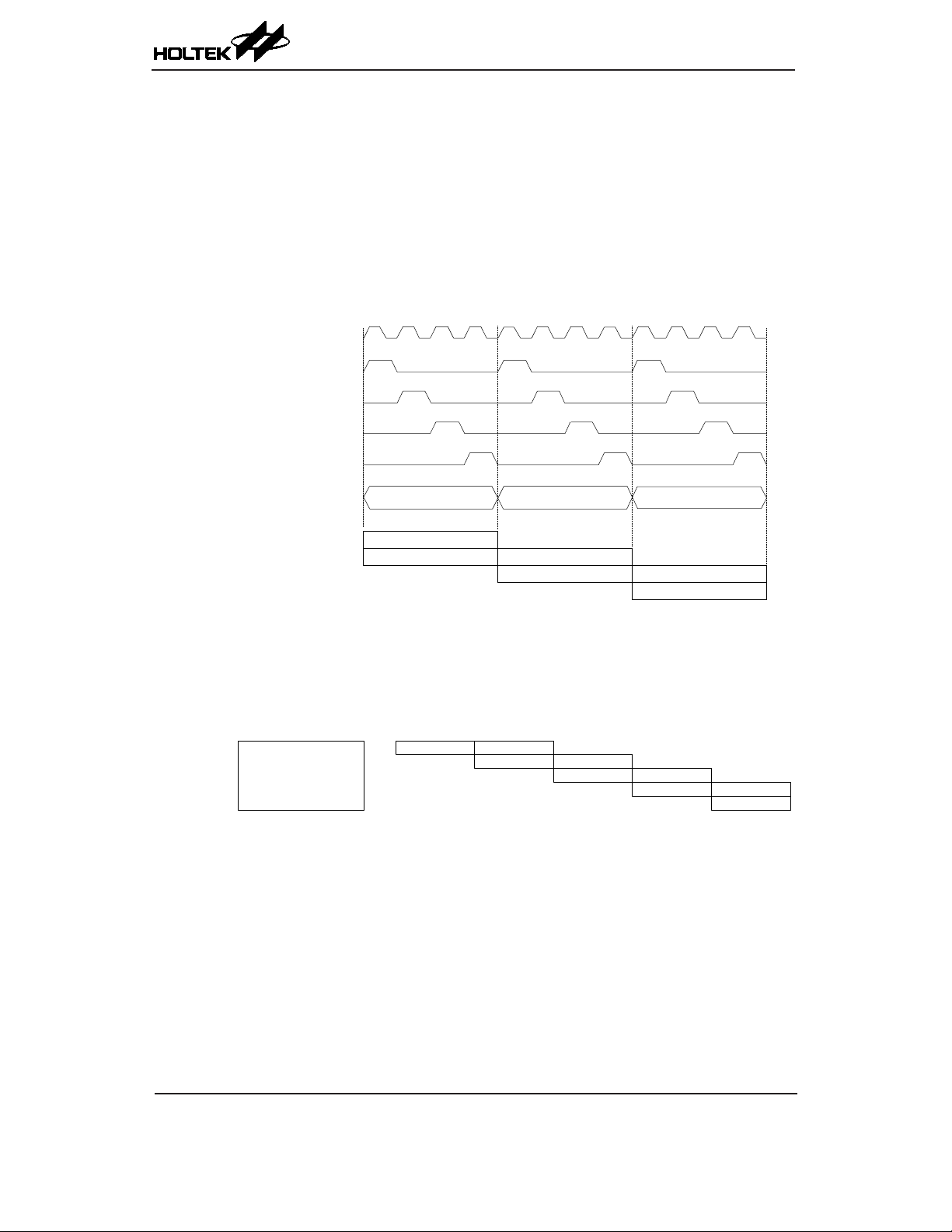
Clocking and Pipelining
Execute Inst. 1
Fetch Inst. 2
1 MOV A, [12H]
2 CALL DELAY
3 CPL [12H]
4:
5:
6 DELAY: NOP
Fetch Inst. 1
Execute Inst. 2
Fetch Inst. 3 Flush Pipeline
Fetch Inst. 6 Execute Inst. 6
Fetch Inst. 7
The main system clock, derived from either a HXT, LXT, HIRC or LIRC oscillator is subdivided
into four internally generated non-overlapping clocks, T1~T4. The Program Counter is incremented
at the beginning of the T1 clock during which time a new instruction is fetched. The remaining
T2~T4 clocks carry out the decoding and execution functions. In this way, one T1~T4 clock
cycle forms one instruction cycle. Although the fetching and execution of instructions takes place
in consecutive instruction cycles, the pipelining structure of the microcontroller ensures that
instructions are effectively executed in one instruction cycle. The exception to this are instructions
where the contents of the Program Counter are changed, such as subroutine calls or jumps, in which
case the instruction will take one more instruction cycle to execute.
Oscillator Clock
(System Clock)
Phase Clock T1
Phase Clock T2
Phase Clock T3
Phase Clock T4
HT45F4050
A/D NFC Flash MCU
Program Counter
For instructions involving branches, such as jump or call instructions, two machine cycles are
required to complete instruction execution. An extra cycle is required as the program takes one
cycle to rst obtain the actual jump or call address and then another cycle to actually execute the
branch. The requirement for this extra cycle should be taken into account by programmers in timing
sensitive applications.
Program Counter
During program execution, the Program Counter is used to keep track of the address of the
next instruction to be executed. It is automatically incremented by one each time an instruction
is executed except for instructions, such as "JMP" or "CALL" that demands a jump to a non-
consecutive Program Memory address. Only the lower 8 bits, known as the Program Counter Low
Register, are directly addressable by the application program.
When executing instructions requiring jumps to non-consecutive addresses such as a jump instruction,
a subroutine call, interrupt or reset, etc., the microcontroller manages program control by loading
the required address into the Program Counter. For conditional skip instructions, once the condition
has been met, the next instruction, which has already been fetched during the present instruction
execution, is discarded and a dummy cycle takes its place while the correct instruction is obtained.
Pipelining
PC
Fetch Inst. (PC)
Execute Inst. (PC-1)
System Clocking and Pipelining
Instruction Fetching
PC+1
Fetch Inst. (PC+1)
Execute Inst. (PC)
PC+2
Fetch Inst. (PC+2)
Execute Inst. (PC+1)
Rev. 1.00 26 September 11, 2018 Rev. 1.00 27 September 11, 2018
Page 27
HT45F4050
A/D NFC Flash MCU
The lower byte of the Program Counter, known as the Program Counter Low register or PCL, is
available for program control and is a readable and writeable register. By transferring data directly
into this register, a short program jump can be executed directly. However, as only this low byte
is available for manipulation, the jumps are limited to the present page of memory that is 256
locations. When such program jumps are executed it should also be noted that a dummy cycle
will be inserted. Manipulating the PCL register may cause program branching, so an extra cycle is
needed to pre-fetch.
Stack
This is a special part of the memory which is used to save the contents of the Program Counter only.
The stack is organized into multiple levels and neither part of the data nor part of the program space,
and is neither readable nor writeable. The activated level is indexed by the Stack Pointer, and is
neither readable nor writeable. At a subroutine call or interrupt acknowledge signal, the contents of
the Program Counter are pushed onto the stack. At the end of a subroutine or an interrupt routine,
signaled by a return instruction, RET or RETI, the Program Counter is restored to its previous value
from the stack. After a device reset, the Stack Pointer will point to the top of the stack.
If the stack is full and an enabled interrupt takes place, the interrupt request ag will be recorded but
the acknowledge signal will be inhibited. When the Stack Pointer is decremented, by RET or RETI,
the interrupt will be serviced. This feature prevents stack overow allowing the programmer to use
the structure more easily. However, when the stack is full, a CALL subroutine instruction can still
be executed which will result in a stack overow. Precautions should be taken to avoid such cases
which might cause unpredictable program branching.
If the stack is overow, the rst Program Counter save in the stack will be lost.
Program Counter
High Byte Low Byte (PCL)
PC12~PC8 PCL7~PCL0
Program Counter
Top of Stack
Stack
Pointer
Bottom of Stack
Arithmetic and Logic Unit – ALU
The arithmetic-logic unit or ALU is a critical area of the microcontroller that carries out arithmetic
and logic operations of the instruction set. Connected to the main microcontroller data bus, the ALU
receives related instruction codes and performs the required arithmetic or logical operations after
which the result will be placed in the specied register. As these ALU calculation or operations may
result in carry, borrow or other status changes, the status register will be correspondingly updated to
reect these changes. The ALU supports the following functions:
• Arithmetic operations:
ADD, ADDM, ADC, ADCM, SUB, SUBM, SBC, SBCM, DAA,
LADD, LADDM, LADC, LADCM, LSUB, LSUBM, LSBC, LSBCM, LDAA
Stack Level 1
Stack Level 2
Stack Level 3
:
:
:
Stack Level 8
Program Counter
Program Memory
Page 28

• Logic operations:
AND, OR, XOR, ANDM, ORM, XORM, CPL, CPLA,
LAND, LANDM, LOR, LORM, LXOR, LXORM, LCPL, LCPLA
• Rotation:
RRA, RR, RRCA, RRC, RLA, RL, RLCA, RLC,
LRR, LRRA, LRRCA, LRRC, LRLA, LRL, LRLCA, LRLC
• Increment and Decrement:
INCA, INC, DECA, DEC,
LINCA, LINC, LDECA, LDEC
• Branch decision:
JMP, SZ, SZA, SNZ, SIZ, SDZ, SIZA, SDZA, CALL, RET, RETI,
LSNZ, LSZ, LSZA, LSIZ, LSIZA, LSDZ, LSDZA
Flash Program Memory
The Program Memory is the location where the user code or program is stored. For this device the
Program Memory is Flash type, which means it can be programmed and re-programmed a large
number of times, allowing the user the convenience of code modication on the same device. By using
the appropriate programming tools, the Flash device offer users the exibility to conveniently debug
and develop their applications while also offering a means of eld programming and updating.
HT45F4050
A/D NFC Flash MCU
Structure
The Program Memory has a capacity of 8K×16 bits. The Program Memory is addressed by the
Program Counter and also contains data, table information and interrupt entries. Table data, which can
be setup in any location within the Program Memory, is addressed by a separate table pointer register.
Special Vectors
Within the Program Memory, certain locations are reserved for the reset and interrupts. The location
000H is reserved for use by the device reset for program initialisation. After a device reset is
initiated, the program will jump to this location and begin execution.
000H
004H
030H
n00H
nFFH
1FFFH
Program Memory Structure
Initialisation Vector
Interrupt Vectors
Look-up Table
16 bits
Rev. 1.00 28 September 11, 2018 Rev. 1.00 29 September 11, 2018
Page 29
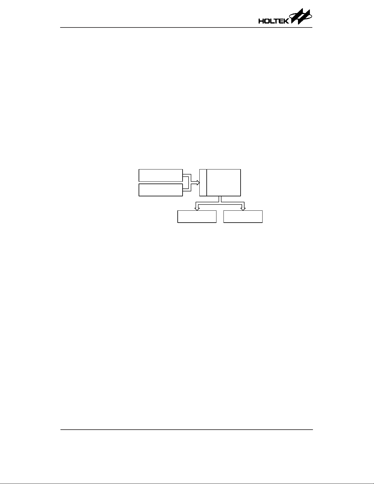
HT45F4050
A/D NFC Flash MCU
Look-up Table
Any location within the Program Memory can be dened as a look-up table where programmers can
store xed data. To use the look-up table, the table pointer must rst be setup by placing the address
of the look up data to be retrieved in the table pointer register, TBLP and TBHP. These registers
dene the total address of the look-up table.
After setting up the table pointer pair, the table data can be retrieved from the Program Memory
using the corresponding table read instruction such as "TABRD [m]" or "TABRDL [m]" respectively
when the memory [m] is located in sector 0. If the memory [m] is located in other sectors, the data
can be retrieved from the program memory using the corresponding extended table read instruction
such as "LTABRD [m]" or "LTABRDL [m]" respectively. When the instruction is executed, the
lower order table byte from the Program Memory will be transferred to the user defined Data
Memory register [m] as specified in the instruction. The higher order table data byte from the
Program Memory will be transferred to the TBLH special register.
The accompanying diagram illustrates the addressing data ow of the look-up table.
Last Page or
TBHP Register
TBLP Register
Program Memory
Address
Data
16 bits
Table Program Example
The following example shows how the table pointer and table data is dened and retrieved from the
microcontroller. This example uses raw table data located in the Program Memory which is stored
there using the ORG statement. The value at this ORG statement is "1F00H" which refers to the
start address of the last page within the 8K words Program Memory. The table pointer low byte
register is setup here to have an initial value of "06H". This will ensure that the rst data read from
the data table will be at the Program Memory address "1F06H" or 6 locations after the start of the
last page. Note that the value for the table pointer is referenced to the specic address pointed by
the TBLP and TBHP registers if the "TABRD [m]" or "LTABRD [m]" instruction is being used. The
high byte of the table data which in this case is equal to zero will be transferred to the TBLH register
automatically when the "TABRD [m]" or "LTABRD [m]" instruction is executed.
Because the TBLH register is a read/write register and can be restored, care should be taken
to ensure its protection if both the main routine and Interrupt Service Routine use table read
instructions. If using the table read instructions, the Interrupt Service Routines may change the
value of the TBLH and subsequently cause errors if used again by the main routine. As a rule it is
recommended that simultaneous use of the table read instructions should be avoided. However, in
situations where simultaneous use cannot be avoided, the interrupts should be disabled prior to the
execution of any main routine table-read instructions. Note that all table related instructions require
two instruction cycles to complete their operation.
Register TBLH
High Byte Low Byte
User Selected
Register
Page 30
Table Read Program Example
tempreg1 db ? ; temporary register #1
tempreg2 db ? ; temporary register #2
:
mov a,06h ; initialise low table pointer - note that this address is referenced
mov tblp,a ; to the last page or the page that tbhp pointed
mo v a,1Fh ; initialise high table pointer
mov tbhp,a ; it is not necessary to set tbhp if executing tabrdl or ltabrdl
:
tabrd tempreg1 ; transfers value in table referenced by table pointer,
dec tblp ; reduce value of table pointer by one
tabrd tempreg2 ; transfers value in table referenced by table pointer,
; register tempreg2
; the value "00H" will be transferred to the high byte register TBLH
:
org 1F00h ; sets initial address of program memory
dc 00Ah, 00Bh, 00Ch, 00Dh, 00Eh, 00Fh, 01Ah, 01Bh
:
; data at program memory address "1F06H" transferred to tempreg1 and TBLH
; data at program memory address "1F05H" transferred to tempreg2 and TBLH
; in this example the data "1AH" is transferred to tempreg1 and data "0FH" to
In Circuit Programming – ICP
The provision of Flash type Program Memory provides the user with a means of convenient and
easy upgrades and modications to their programs on the same device.
As an additional convenience, Holtek has provided a means of programming the microcontroller in-
circuit using a 4-pin interface. This provides manufacturers with the possibility of manufacturing
their circuit boards complete with a programmed or un-programmed microcontroller, and then
programming or upgrading the program at a later stage. This enables product manufacturers to easily
keep their manufactured products supplied with the latest program releases without removal and re-
insertion of the device.
Holtek Writer Pins MCU Programming Pins Pin Description
ICPDA PA0 Programming Serial Data/Address
ICPCK PA2 Programming Clock
VDD VDD&AVDD Power Supply
VSS VSS&AVSS&VSSN Ground
HT45F4050
A/D NFC Flash MCU
The Program Memory and EEPROM data Memory can both be programmed serially in-circuit using
this 4-wire interface. Data is downloaded and uploaded serially on a single pin with an additional
line for the clock. Two additional lines are required for the power supply. The technical details
regarding the in-circuit programming of the device are beyond the scope of this document and will
be supplied in supplementary literature.
During the programming process, the user must take control of the ICPDA and ICPCK pins for data
and clock programming purposes to ensure that no other outputs are connected to these two pins.
Rev. 1.00 30 September 11, 2018 Rev. 1.00 31 September 11, 2018
Page 31
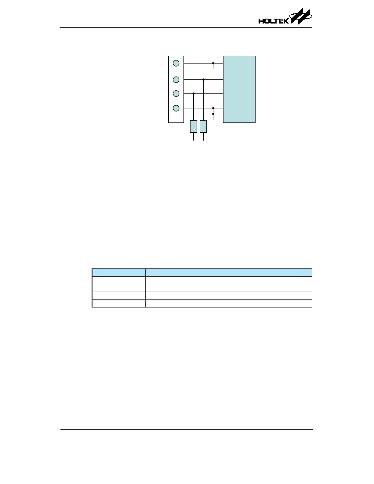
HT45F4050
A/D NFC Flash MCU
Writer Connector
Writer_VDD
ICPDA
ICPCK
Writer_VSS
Note: * may be resistor or capacitor. The resistance of * must be greater than 1kΩ or the capacitance
of * must be less than 1nF.
On-Chip Debug Support – OCDS
There is an EV chip named HT45V4050, which is used to emulate HT45F4050 device. The EV
chip device also provides an "On-Chip Debug" function to debug the real MCU device during the
development process. The EV chip and the actual MCU device are almost functionally compatible
except for the "On-Chip Debug" function. Users can use the EV chip device to emulate the real chip
device behavior by connecting the OCDSDA and OCDSCK pins to the Holtek HT-IDE development
tools. The OCDSDA pin is the OCDS Data/Address input/output pin while the OCDSCK pin is the
OCDS clock input pin. When users use the EV chip for debugging, other functions which are shared
with the OCDSDA and OCDSCK pins in the actual MCU device will have no effect in the EV chip.
However, the two OCDS pins which are pin-shared with the ICP programming pins are still used as
the Flash Memory programming pins for ICP. For a more detailed OCDS description, refer to the
corresponding document named "Holtek e-Link for 8-bit MCU OCDS User’s Guide".
Holtek e-Link Pins EV Chip Pins Pin Description
OCDSDA OCDSDA On-chip Debug Support Data/Address input/output
OCDSCK OCDSCK On-chip Debug Support Clock input
VDD VDD&AVDD Power Supply
VSS VSS&AVSS&VSSN Ground
Signals
*
*
To other Circuit
MCU Programming
Pins
VDD
AVDD
PA0
PA2
VSS
AVSS
VSSN
Data Memory
The Data Memory is a volatile area of 8-bit wide RAM internal memory and is the location where
temporary information is stored.
Divided into two types, the rst of Data Memory is an area of RAM where special function registers
are located. These registers have fixed locations and are necessary for correct operation of the
device. Many of these registers can be read from and written to directly under program control,
however, some remain protected from user manipulation. The second area of Data Memory is
reserved for general purpose use. All locations within this area are read and write accessible under
program control.
Switching between the different Data Memory sectors is achieved by properly setting the Memory
Pointers to correct value if using indirect addressing method.
Page 32

Structure
The Data Memory is subdivided into several sectors, all of which are implemented in 8-bit wide
Memory. Each of the Data Memory Sectors is categorized into two types, the special Purpose Data
Memory and the General Purpose Data Memory.
The address range of the Special Purpose Data Memory for the devices is from 00H to 7FH while
the General Purpose Data Memory address range is from 80H to FFH.
A/D NFC Flash MCU
Special Purpose Data Memory General Purpose Data Memory
Located Sectors Capacity Sector: Address
0, 1 256×8
Data Memory Summary
00H
Special Purpose
Data Memory
(Sector 0 ~ Sector 1)
7FH
80H
0: 80H~FFH
1: 80H~FFH
EEC in Sector 1
40H
HT45F4050
General Purpose Data Memory
(Sector 0 ~ Sector 1)
Data Memory Addressing
For this device that supports the extended instructions, there is no Bank Pointer for Data Memory.
For Data Memory the desired Sector is pointed by the MP1H or MP2H register and the certain
Data Memory address in the selected sector is specied by the MP1L or MP2L register when using
indirect addressing access.
Direct Addressing can be used in all sectors using the corresponding instruction which can address
all available data memory space. For the accessed data memory which is located in any data memory
sectors except sector 0, the extended instructions can be used to access the data memory instead
of using the indirect addressing access. The main difference between standard instructions and
extended instructions is that the data memory address "m" in the extended instructions has 9 valid
bits, the high byte indicates a sector and the low byte indicates a specic address.
General Purpose Data Memory
All microcontroller programs require an area of read/write memory where temporary data can be
stored and retrieved for use later. It is this area of RAM memory that is known as General Purpose
Data Memory. This area of Data Memory is fully accessible by the user programing for both reading
and writing operations. By using the bit operation instructions individual bits can be set or reset
under program control giving the user a large range of exibility for bit manipulation in the Data
Memory.
FFH
Data Memory Structure
Sector 0
Sector 1
Rev. 1.00 32 September 11, 2018 Rev. 1.00 33 September 11, 2018
Page 33

HT45F4050
: unused, read as 00H
A/D NFC Flash MCU
Special Purpose Data Memory
This area of Data Memory is where registers, necessary for the correct operation of the
microcontroller, are stored. Most of the registers are both readable and writeable but some are
protected and are readable only, the details of which are located under the relevant Special Function
Register section. Note that for locations that are unused, any read instruction to these addresses will
return the value "00H".
00H
01H
02H
03H
04H
05H
06H
07H
08H
09H
0AH
0BH
0CH
0DH
0EH
0FH
10H
11H
12H
13H
14H
15H
16H
17H
18H
19H
1AH
1BH
1CH
1DH
1EH
1FH
20H
21H
22H
23H
24H
28H
29H
2AH
2BH
2CH
2DH
2EH
2FH
30H
31H
32H
33H
34H
35H
36H
37H
38H
39H
3AH
3BH
3CH
3DH
3EH
3FH
Sector 0 Sector 1
IAR0
MP0
IAR1
MP1L
MP1H
ACC
PCL
TBLP
TBLH
TBHP
STATUS
IAR2
MP2L
MP2H
RSTFC
INTC0
INTC1
INTC2
INTC3
PA
PAC
PAPU
PAWU
PB
PBC
PBPU
PC
PCC
PCPU
PD
PDC
PDPU
PE
PEC
PEPU
PF
PFC25H
PFPU26H
RSTC27H
VBGRC
MFI0
MFI1
MFI2
INTEG
PMPS
SCC
HIRCC
HXTC
LXTC
WDTC
LVRC
LVDC
LVPUC
CMPC
CMPVOS
CTMC0
CTMC1
CTMDL
CTMDH
CTMAL
CTMAH
CTMRP
NFC_INTE
NFC_INTF
NFC_STATUS
NFCCTRL
NFCEEC
NFCEEA
NFCEED0
NFCEED1
NFCEED2
NFCEED3
NFCWRA
40H
41H
42H
43H
44H
45H
46H
47H
48H
49H
4AH
4BH
4CH
4DH
4EH
4FH
50H
51H
52H
53H
54H
55H
56H
57H
58H
59H
5AH
5BH
5CH
5DH
5EH
5FH
60H
61H
62H
63H
64H
68H
69H
6AH
6BH
6CH
6DH
6EH
6FH
70H
71H
72H
73H
74H
75H
76H
77H
78H
79H
7AH
7BH
7CH
7FH
Sector 0 Sector 1
EEA
EED
PTMC0
PTMC1
PTMDL
PTMDH
PTMAL
PTMAH
PTMRPL
PTMRPH
STMC0
STMC1
STMDL
STMDH
STMAL
STMAH
STMRP
SLEDC0
SLEDC1
SLEDC2
TB0C
TB1C
PSC0R
PSC1R
SADOL
SADOH
SADC0
SADC1
SADC2
SIMC0
SIMC1
SIMD
SIMC2/SIMA
SIMTOC
SCOMC65H
USR66H
UCR167H
UCR2
TXR_RXR
BRG
IFS0
IFS1
PAS0
PAS1
PBS0
PBS1
PCS0
PCS1
PDS0
PES0
PES1
PFS0
PFS1
EEC
Special Purpose Data Memory
Page 34

Special Function Register Description
Most of the Special Function Register details will be described in the relevant functional section,
however several registers require a separate description in this section.
Indirect Addressing Registers – IAR0, IAR1, IAR2
The Indirect Addressing Registers, IAR0, IAR1 and IAR2, although having their locations in normal
RAM register space, do not actually physically exist as normal registers. The method of indirect
addressing for RAM data manipulation uses these Indirect Addressing Registers and Memory
Pointers, in contrast to direct memory addressing, where the actual memory address is specied.
Actions on the IAR0, IAR1 and IAR2 registers will result in no actual read or write operation to
these registers but rather to the memory location specied by their corresponding Memory Pointers,
MP0, MP1L/MP1H or MP2L/MP2H. Acting as a pair, IAR0 and MP0 can together access data
from Sector 0 while the IAR1 register together with MP1L/MP1H register pair and IAR2 register
together with MP2L/MP2H register pair can access data from any sector. As the Indirect Addressing
Registers are not physically implemented, reading the Indirect Addressing Registers directly will
return a result of "00H" and writing to the registers directly will result in no operation.
Memory Pointers – MP0, MP1L/MP1H, MP2L/MP2H
Five Memory Pointers, known as MP0, MP1L, MP1H, MP2L and MP2H are provided. These
Memory Pointers are physically implemented in the Data Memory and can be manipulated in the
same way as normal registers providing a convenient way with which to address and track data.
When any operation to the relevant Indirect Addressing Registers is carried out, the actual address
that the microcontroller is directed to is the address specied by the related Memory Pointer. MP0,
together with Indirect Addressing Register, IAR0, are used to access data from Sector 0, while MP1L/
MP1H together with IAR1 and MP2L/MP2H together with IAR2 are used to access data from all
sectors according to the corresponding MP1H or MP2H register. Direct Addressing can be used in all
sectors using the correspongding instruction which can address all available data memory space.
The following example shows how to clear a section of four Data Memory locations already dened
as locations adres1 to adres4.
HT45F4050
A/D NFC Flash MCU
Indirect Addressing Program Example
Example 1
data .section ´data´
adres1 db ?
adres2 db ?
adres3 db ?
adres4 db ?
block db ?
code .section at 0 ´code´
org 00h
start:
mov a,04h ; setup size of block
mo v block,a
mova,offsetadres1 ;AccumulatorloadedwithrstRAMaddress
movmp0,a ;setupmemorypointerwithrstRAMaddress
loo p:
clrIAR0 ;clearthedataataddressdenedbymp0
inc mp0 ; increment memory pointer
sdz block ; check if last memory location has been cleared
jm p loop
continue:
Rev. 1.00 34 September 11, 2018 Rev. 1.00 35 September 11, 2018
Page 35

HT45F4050
A/D NFC Flash MCU
Example 2
data .section ‘data’
adres1 db ?
adres2 db ?
adres3 db ?
adres4 db ?
block db ?
code .section at 0 ‘code’
org 00h
start:
mov a,04h ; setup size of block
mo v block,a
mov a,01h ; setup the memory sector
mo v mp1h,a
mov a,offset adres1 ;AccumulatorloadedwithrstRAMaddress
movmp1l,a ;setupmemorypointerwithrstRAMaddress
loo p:
clrIAR1;clearthedataataddressdenedbyMP1L
incmp1l ;incrementmemorypointerMP1L
sdz block ; check if last memory location has been cleared
jmp loop
continue:
:
The important point to note here is that in the example shown above, no reference is made to specic
Data Memory addresses.
Direct Addressing Program Example using extended instructions
data .section ‘data’
temp db ?
code .section at 0 code
org 00h
start:
lmov a,[m] ; move [m] data to acc
lsub a, [m+1] ; compare [m] and [m+1] data
snz c ; [m]>[m+1]?
jmp continue ; no
lmov a,[m] ; yes, exchange [m] and [m+1] data
mo v te m p,a
lmov a,[m+1]
lmov [m],a
mo v a,tem p
lmov [m+1],a
continue:
:
Note: here "m" is a data memory address located in any data memory sectors. For example,
m=1F0H, it indicates address 0F0H in Sector 1.
Page 36

Accumulator – ACC
The Accumulator is central to the operation of any microcontroller and is closely related with
operations carried out by the ALU. The Accumulator is the place where all intermediate results
from the ALU are stored. Without the Accumulator it would be necessary to write the result of
each calculation or logical operation such as addition, subtraction, shift, etc., to the Data Memory
resulting in higher programming and timing overheads. Data transfer operations usually involve
the temporary storage function of the Accumulator; for example, when transferring data between
one user-defined register and another, it is necessary to do this by passing the data through the
Accumulator as no direct transfer between two registers is permitted.
Program Counter Low Register – PCL
To provide additional program control functions, the low byte of the Program Counter is made
accessible to programmers by locating it within the Special Purpose area of the Data Memory. By
manipulating this register, direct jumps to other program locations are easily implemented. Loading
a value directly into this PCL register will cause a jump to the specied Program Memory location,
however, as the register is only 8-bit wide, only jumps within the current Program Memory page are
permitted. When such operations are used, note that a dummy cycle will be inserted.
Look-up Table Registers – TBLP, TBHP, TBLH
These three special function registers are used to control operation of the look-up table which is
stored in the Program Memory. TBLP and TBHP are the table pointers and indicate the location
where the table data is located. Their value must be setup before any table read commands are
executed. Their value can be changed, for example using the "INC" or "DEC" instructions, allowing
for easy table data pointing and reading. TBLH is the location where the high order byte of the table
data is stored after a table read data instruction has been executed. Note that the lower order table
data byte is transferred to a user dened location.
HT45F4050
A/D NFC Flash MCU
Status Register – STATUS
This 8-bit register contains the zero ag (Z), carry ag (C), auxiliary carry ag (AC), overow ag
(OV), SC ag, CZ ag, power down ag (PDF), and watchdog time-out ag (TO). These arithmetic/
logical operation and system management ags are used to record the status and operation of the
microcontroller.
With the exception of the TO and PDF ags, bits in the status register can be altered by instructions
like most other registers. Any data written into the status register will not change the TO or PDF
flag. In addition, operations related to the status register may give different results due to the
different instruction operations. The TO ag can be affected only by a system power-up, a WDT
time-out or by executing the "CLR WDT" or "HALT" instruction. The PDF ag is affected only by
executing the "HALT" or "CLR WDT" instruction or during a system power-up.
The Z, OV, AC, C SC and CZ ags generally reect the status of the latest operations.
• C is set if an operation results in a carry during an addition operation or if a borrow does not take
place during a subtraction operation; otherwise C is cleared. C is also affected by a rotate through
carry instruction.
• AC is set if an operation results in a carry out of the low nibbles in addition, or no borrow from
the high nibble into the low nibble in subtraction; otherwise AC is cleared.
• Z is set if the result of an arithmetic or logical operation is zero; otherwise Z is cleared.
• OV is set if an operation results in a carry into the highest-order bit but not a carry out of the
highest-order bit, or vice versa; otherwise OV is cleared.
Rev. 1.00 36 September 11, 2018 Rev. 1.00 37 September 11, 2018
Page 37

HT45F4050
A/D NFC Flash MCU
• PDF is cleared by a system power-up or executing the "CLR WDT" instruction. PDF is set by
executing the "HALT" instruction.
• TO is cleared by a system power-up or executing the "CLR WDT" or "HALT" instruction. TO is
set by a WDT time-out.
• CZ is the operational result of different ags for different instructions. Refer to register
denitions for more details.
• SC is the result of the "XOR" operation which is performed by the OV ag and the MSB of the
current instruction operation result.
In addition, on entering an interrupt sequence or executing a subroutine call, the status register will
not be pushed onto the stack automatically. If the contents of the status registers are important and if
the subroutine can corrupt the status register, precautions must be taken to correctly save it.
• STATUS Register
Bit 7 6 5 4 3 2 1 0
Name SC CZ TO PDF OV Z AC C
R/W R/W R/W R R R/W R/W R/W R/W
POR x x 0 0 x x x x
Bit 7 SC: The result of the "XOR" operation which is performed by the OV ag and the
MSB of the instruction operation result.
Bit 6 CZ: The the operational result of different ags for different instuctions.
For SUB/SUBM/LSUB/LSUBM instructions, the CZ ag is equal to the Z ag.
For SBC/SBCM/LSBC/LSBCM instructions, the CZ flag is the "AND" operation
result which is performed by the previous operation CZ ag and current operation zero
ag.
For other instructions, the CZ ag willl not be affected.
Bit 5 TO: Watchdog Time-Out ag
Bit 4 PDF: Power down ag
Bit 3 OV: Overow ag
Bit 2 Z: Zero ag
Bit 1 AC: Auxiliary ag
Bit 0 C: Carry ag
The C ag is also affected by a rotate through carry instruction.
"x": unknown
0: After power up or executing the "CLR WDT" or "HALT" instruction
1: A watchdog time-out occurred.
0: After power up or executing the "CLR WDT" instruction
1: By executing the "HALT" instruction
0: no overow
1: an operation results in a carry into the highest-order bit but not a carry out of the
highest-order bit or vice versa.
0: The result of an arithmetic or logical operation is not zero
1: The result of an arithmetic or logical operation is zero
0: no auxiliary carry
1: an operation results in a carry out of the low nibbles in addition, or no borrow
from the high nibble into the low nibble in subtraction
0: no carry-out
1: an operation results in a carry during an addition operation or if a borrow does not
take place during a subtraction operation
Page 38

EEPROM Data Memory
The device contains an area of internal EEPROM Data Memory. EEPROM is by its nature a
non-volatile form of memory, with data retention even when its power supply is removed. By
incorporating this kind of data memory, a whole new host of application possibilities are made
available to the designer. The availability of EEPROM storage allows information such as product
identification numbers, calibration values, specific user data, system setup data or other product
information to be stored directly within the product microcontroller. The process of reading and
writing data to the EEPROM memory has been reduced to a very trivial affair.
EEPROM Data Memory Structure
The EEPROM Data Memory capacity is 64×8 bits. Unlike the Program Memory and RAM Data
Memory, the EEPROM Data Memory is not directly mapped and is therefore not directly accessible
in the same way as the other types of memory. Read and Write operations to the EEPROM are
carried out in single byte operations using an address and data register in Sector 0 and a single
control register in Sector 1.
EEPROM Registers
Three registers control the overall operation of the internal EEPROM Data Memory. These are the
address register, EEA, the data register, EED and a single control register, EEC. As both the EEA
and EED registers are located in Sector 0, they can be directly accessed in the same way as any other
Special Function Register. The EEC register however, being located in Sector 1, can be addressed
directly using the corresponding extended instructions or can be read from or written to indirectly
using the MP1H/MP1L or MP2H/MP2L Memory Pointer pairs and Indirect Addressing Register,
IAR1 or IAR2. Because the EEC control register is located at address 40H in Sector 1, the Memory
Pointer low byte register, MP1L or MP2L, must rst be set to the value 40H and the Memory Pointer
high byte register, MP1H or MP2H, set to the value, 01H, before any operations on the EEC register
are executed.
Register
Name
EEA — — EEA5 EEA4 EEA3 EEA2 EEA1 EEA0
EED D7 D6 D5 D4 D3 D2 D1 D0
EEC — — — — WREN WR RDEN RD
7 6 5 4 3 2 1 0
HT45F4050
A/D NFC Flash MCU
Bit
EEPROM Control Registers List
• EEA Register
Bit 7 6 5 4 3 2 1 0
Name — — EEA5 EEA4 EEA3 EEA2 EEA1 EEA0
R/W — — R/W R/W R/W R/W R/W R/W
POR — — 0 0 0 0 0 0
Bit 7 ~ 6 Unimplemented, read as "0"
Bit 5 ~ 0 EEA5~EEA0: Data EEPROM address bit 5 ~ bit 0
Rev. 1.00 38 September 11, 2018 Rev. 1.00 39 September 11, 2018
Page 39

HT45F4050
A/D NFC Flash MCU
• EED Register
Bit 7 6 5 4 3 2 1 0
Name D7 D6 D5 D4 D3 D2 D1 D0
R/W R/W R/W R/W R/W R/W R/W R/W R/W
POR 0 0 0 0 0 0 0 0
Bit 7 ~ 0 D7~D0: Data EEPROM data bit 7 ~ bit 0
• EEC Register
Bit 7 6 5 4 3 2 1 0
Name — — — — WREN WR RDEN RD
R/W — — — — R/W R/W R/W R/W
POR — — — — 0 0 0 0
Bit 7 ~ 4 Unimplemented, read as "0"
Bit 3 WREN: Data EEPROM Write Enable
This is the Data EEPROM Write Enable Bit which must be set high before Data
EEPROM write operations are carried out. Clearing this bit to zero will inhibit Data
EEPROM write operations.
Bit 2 WR: EEPROM Write Control
This is the Data EEPROM Write Control Bit and when set high by the application
program will activate a write cycle. This bit will be automatically reset to zero by the
hardware after the write cycle has nished. Setting this bit high will have no effect if
the WREN has not rst been set high.
Bit 1 RDEN: Data EEPROM Read Enable
This is the Data EEPROM Read Enable Bit which must be set high before Data
EEPROM read operations are carried out. Clearing this bit to zero will inhibit Data
EEPROM read operations.
Bit 0 RD: EEPROM Read Control
This is the Data EEPROM Read Control Bit and when set high by the application
program will activate a read cycle. This bit will be automatically reset to zero by the
hardware after the read cycle has nished. Setting this bit high will have no effect if
the RDEN has not rst been set high.
Note that the WREN, WR, RDEN and RD bits can not be set to "1" at the same time
in one instruction. The WR and RD can not be set to "1" at the same time.
0: Disable
1: Enable
0: Write cycle has nished
1: Activate a write cycle
0: Disable
1: Enable
0: Read cycle has nished
1: Activate a read cycle
Reading Data from the EEPROM
To read data from the EEPROM, The EEPROM address of the data to be read must then be placed
in the EEA register. Then the read enable bit, RDEN, in the EEC register must first be set high
to enable the read function. If the RD bit in the EEC register is now set high, a read cycle will be
initiated. Setting the RD bit high will not initiate a read operation if the RDEN bit has not been set.
When the read cycle terminates, the RD bit will be automatically cleared to zero, after which the
data can be read from the EED register. The data will remain in the EED register until another read
or write operation is executed. The application program can poll the RD bit to determine when the
data is valid for reading.
Page 40

Writing Data to the EEPROM
To write data to the EEPROM, the EEPROM address of the data to be written must rst be placed
in the EEA register and the data placed in the EED register. Then the write enable bit, WREN,
in the EEC register must first be set high to enable the write function. After this, the WR bit in
the EEC register must be immediately set high to initial a write cycle. These two instructions
must be executed consecutively. The global interrupt bit EMI should also first be cleared before
implementing any write operations, and then set again after the write cycle has started. Note that
setting the WR bit high will not initiate a write cycle if the WREN bit has not been set. As the
EEPROM write cycle is controlled using an internal timer whose operation is asynchronous to
microcontroller system clock, a certain time will elapse before the data will have been written into
the EEPROM. Detecting when the write cycle has nished can be implemented either by polling the
WR bit in the EEC register or by using the EEPROM interrupt. When the write cycle terminates,
the WR bit will be automatically cleared to zero by the microcontroller, informing the user that the
data has been written to the EEPROM. The application program can therefore poll the WR bit to
determine when the write cycle has ended.
Write Protection
Protection against inadvertent write operation is provided in several ways. After the device is
powered on the Write Enable bit in the control register will be cleared preventing any write
operations. Also at power-on the Memory Pointer high byte register, MP1H or MP2H, will be reset
to zero, which means that Data Memory Sector 0 will be selected. As the EEPROM control register
is located in Sector 1, this adds a further measure of protection against spurious write operations.
During normal program operation, ensuring that the Write Enable bit in the control register is
cleared will safeguard against incorrect write operations.
HT45F4050
A/D NFC Flash MCU
EEPROM Interrupt
The EEPROM write interrupt is generated when an EEPROM write cycle has ended. The EEPROM
interrupt must rst be enabled by setting the DEE bit in the relevant interrupt register. However, as
the EEPROM is contained within a Multi-function Interrupt, the associated multi-function interrupt
enable bit must also be set. When an EEPROM write cycle ends, the DEF request flag and its
associated multi-function interrupt request ag will both be set. If the global, EEPROM and Multi-
function interrupts are enabled and the stack is not full, a jump to the associated Multi-function
Interrupt vector will take place. When the interrupt is serviced only the Multi-function interrupt ag
will be automatically reset, the EEPROM interrupt ag must be manually reset by the application
program.
Rev. 1.00 40 September 11, 2018 Rev. 1.00 41 September 11, 2018
Page 41

HT45F4050
A/D NFC Flash MCU
Programming Considerations
Care must be taken that data is not inadvertently written to the EEPROM. Protection can be
enhanced by ensuring that the Write Enable bit is normally cleared to zero when not writing. Also the
Memory Pointer high byte register could be normally cleared to zero as this would inhibit access to
Sector 1 where the EEPROM control register exist. Although certainly not necessary, consideration
might be given in the application program to the checking of the validity of new write data by a
simple read back process. When writing data the WR bit must be set high immediately after the
WREN bit has been set high, to ensure the write cycle executes correctly. The global interrupt bit
EMI should also be cleared before a write cycle is executed and then re-enabled after the write cycle
starts. Note that the device should not enter the IDLE or SLEEP mode until the EEPROM read or
write operation is totally completed. Otherwise, the EEPROM read or write operation will fail.
Programming Examples
Reading data from the EEPROM – polling method
MOVA,EEPROM_ADRES ;userdenedaddress
MOVEEA,A
MOVA,040H ;setupmemorypointerlowbyteMP1L
MOVMP1L,A ;MP1LpointstoEECregister
MOVA,01H ;setupMemoryPointerhighbyteMP1H
MOVMP1H,A
SETIAR1.1 ;setRDENbit,enablereadoperations
SETIAR1.0 ;startReadCycle-setRDbit
BACK:
SZIAR1.0 ;checkforreadcycleend
JMPBACK
CLRIAR1 ;disableEEPROMread/write
CLRMP1H
MOVA,EED ;movereaddatatoregister
MOVREAD_DATA,A
Writing Data to the EEPROM – polling method
MOVA,EEPROM_ADRES ;userdenedaddress
MOVEEA,A
MOVA,EEPROM_DATA ;userdeneddata
MOVEED,A
MOVA,40H ;setupmemorypointerlowbyteMP1L
MOVMP1L,A ;MP1LpointstoEECregister
MOVA,01H ;setupMemoryPointerhighbyteMP1H
MOVMP1H,A
CLREMI
SETIAR1.3 ;setWRENbit,enablewriteoperations
SETIAR1.2 ;startWriteCycle-setWRbit–executedimmediately
; aftersetWRENbit
SETEMI
BACK:
SZIAR1.2 ;checkforwritecycleend
JMPBACK
CLRIAR1 ;disableEEPROMread/write
CLRMP1H
Page 42
Oscillators
Various oscillator options offer the user a wide range of functions according to their various
application requirements. The flexible features of the oscillator functions ensure that the best
optimisation can be achieved in terms of speed and power saving. Oscillator selections and operation
are selected through a combination of conguration options and relevant control registers.
Oscillator Overview
In addition to being the source of the main system clock the oscillators also provide clock sources
for the Watchdog Timer and Time Base Interrupts. External oscillators requiring some external
components as well as fully integrated internal oscillators, requiring no external components,
are provided to form a wide range of both fast and slow system oscillators. All oscillator options
are selected through the register programming. The higher frequency oscillators provide higher
performance but carry with it the disadvantage of higher power requirements, while the opposite
is of course true for the lower frequency oscillators. With the capability of dynamically switching
between fast and slow system clock, the device has the flexibility to optimize the performance/
power ratio, a feature especially important in power sensitive portable applications.
External High Speed Crystal HXT 400kHz~16MHz OSC1/OSC2
Internal High Speed RC HIRC 4, 8, 12MHz —
External Low Speed Crystal LXT 32.768kHz XT1/XT2
Internal Low Speed RC LIRC 32kHz —
HT45F4050
A/D NFC Flash MCU
Type Name Freq. Pins
Oscillator Types
System Clock Congurations
There are four methods of generating the system clock, two high speed oscillators and two low
speed oscillators. The high speed oscillators are the external crystal/ceramic oscillator – HXT and
the internal 4MHz, 8MHz, 12MHz RC oscillator – HIRC. The two low speed oscillators are the
internal 32kHz RC oscillator – LIRC and the external 32.768kHz crystal oscillator – LXT. Selecting
whether the low or high speed oscillator is used as the system oscillator is implemented using the
CKS2~CKS0 bits in the SCC register and as the system clock can be dynamically selected.
The actual source clock used for the low speed oscillators is chosen by the FSS bit in the SCC
register while for the high speed oscillator the source clock is selected by the FHS bit in the SCC
register. The frequency of the slow speed or high speed system clock is determined using the
CKS2~CKS0 bits in the SCC register. Note that two oscillator selections must be made namely one
high speed and one low speed system oscillators. It is not possible to choose a no-oscillator selection
for either the high or low speed oscillator.
Rev. 1.00 42 September 11, 2018 Rev. 1.00 43 September 11, 2018
Page 43
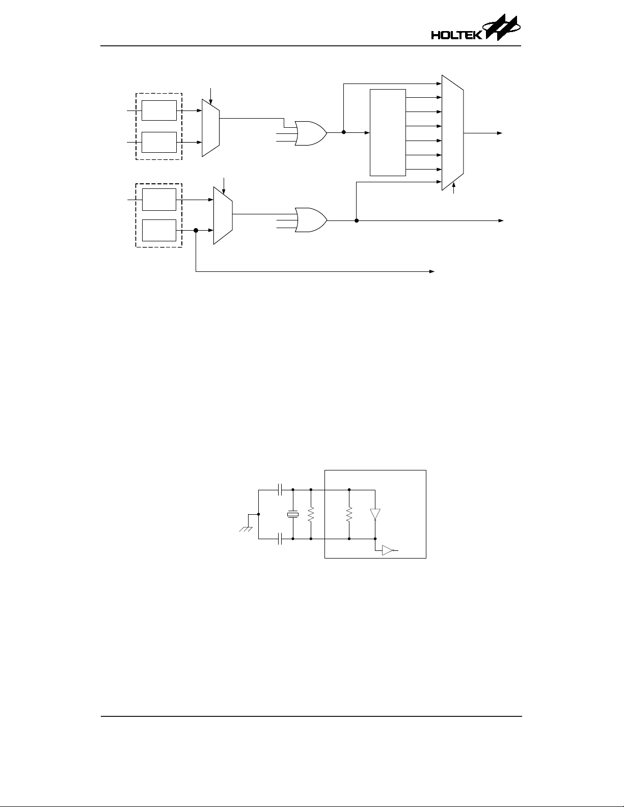
HT45F4050
A/D NFC Flash MCU
HIRCEN
HXTEN
High Speed
Oscillators
HIRC
HXT
FHS
f
H
fH/2
f
/4
H
/8
f
H
f
f
H
FSS
IDLE0
SLEEP
Prescaler
f
/16
H
f
/32
H
f
/64
H
SYS
LXTEN
LXT
LIRC
Low Speed
Oscillators
f
LIRC
IDLE2
SLEEP
System Clock Congurations
External Crystal/Ceramic Oscillator – HXT
The External Crystal/Ceramic System Oscillator is one of the high frequency oscillator choices,
which is selected via a software control bit, FHS. For most crystal oscillator configurations, the
simple connection of a crystal across OSC1 and OSC2 will create the necessary phase shift and
feedback for oscillation, without requiring external capacitors. However, for some crystal types
and frequencies, to ensure oscillation, it may be necessary to add two small value capacitors, C1
and C2. Using a ceramic resonator will usually require two small value capacitors, C1 and C2,
to be connected as shown for oscillation to occur. The values of C1 and C2 should be selected in
consultation with the crystal or resonator manufacturer's specication.
For oscillator stability and to minimise the effects of noise and crosstalk, it is important to ensure
that the crystal and any associated resistors and capacitors along with interconnecting lines are all
located as close to the MCU as possible.
C1
OSC1
f
SUB
f
LIRC
Internal
Oscillator
Circuit
CKS2~CKS0
f
SUB
OSC2
R
F
To internal
circuits
R
P
C2
Note: 1. RPis normally not required. C1 and C2 are required.
2. Although not shown OSC1/OSC2 pins have a parasitic
capacitance of around 7pF.
Crystal/Resonator Oscillator – HXT
Page 44

Crystal Oscillator C1 and C2 Values
Crystal Frequency C1 C2
16MHz 0pF 0pF
12MHz 0pF 0pF
8MHz 0pF 0pF
4MHz 0pF 0pF
1MHz 100pF 100pF
Note: C1 and C2 values are for guidance only.
Crystal Recommended Capacitor Values
Internal RC Oscillator – HIRC
The internal RC oscillator is a fully integrated system oscillator requiring no external components.
The internal RC oscillator has three fixed frequencies of 4MHz, 8MHz, and 12MHz. Device
trimming during the manufacturing process and the inclusion of internal frequency compensation
circuits are used to ensure that the inuence of the power supply voltage, temperature and process
variations on the oscillation frequency are minimised. Note that if this internal system clock option
is selected, it requires no external pins for its operation.
External 32.768kHz Crystal Oscillator – LXT
The External 32.768kHz Crystal System Oscillator is one of the low frequency oscillator choices,
which is selected via a software control bit, FSS. This clock source has a fixed frequency of
32.768kHz and requires a 32.768kHz crystal to be connected between pins XT1 and XT2. The
external resistor and capacitor components connected to the 32.768kHz crystal are necessary to
provide oscillation. For applications where precise frequencies are essential, these components may
be required to provide frequency compensation due to different crystal manufacturing tolerances.
After the LXT oscillator is enabled by setting the LXTEN bit to 1, there is a time delay associated
with the LXT oscillator waiting for it to start-up.
When the microcontroller enters the SLEEP or IDLE Mode, the system clock is switched off to stop
microcontroller activity and to conserve power. However, in many microcontroller applications
it may be necessary to keep the internal timers operational even when the microcontroller is in
the SLEEP or IDLE Mode. To do this, another clock, independent of the system clock, must be
provided.
However, for some crystals, to ensure oscillation and accurate frequency generation, it is necessary
to add two small value external capacitors, C1 and C2. The exact values of C1 and C2 should
be selected in consultation with the crystal or resonator manufacturer specification. The external
parallel feedback resistor, RP, is required.
The pin-shared software control bits determine if the XT1/XT2 pins are used for the LXT oscillator
or as logic I/O or other pin-shared functional pins.
• If the LXT oscillator is not used for any clock source, the XT1/XT2 pins can be used as normal I/O
or other pin-shared functional pins.
• If the LXT oscillator is used for any clock source, the 32.768kHz crystal should be connected to
the XT1/XT2 pins.
For oscillator stability and to minimise the effects of noise and crosstalk, it is important to ensure
that the crystal and any associated resistors and capacitors along with interconnecting lines are all
located as close to the MCU as possible.
HT45F4050
A/D NFC Flash MCU
Rev. 1.00 44 September 11, 2018 Rev. 1.00 45 September 11, 2018
Page 45

HT45F4050
A/D NFC Flash MCU
32.768
Note: 1. RP, C1 and C2 are required.
2. Although not shown XT1/XT2 pins have a parasitic
Crystal Frequency C1 C2
32.768kHz 10pF 10pF
Note: 1. C1 and C2 values are for guidance only.
2. RP=5M~10MΩ is recommended.
32.768kHz Crystal Recommended Capacitor Values
Internal 32kHz Oscillator – LIRC
The Internal 32 kHz System Oscillator is one of the low frequency oscillator choices, which is
selected via a software control bit, FSS. It is a fully integrated RC oscillator with a typical frequency
of 32kHz at full voltage range, requiring no external components for its implementation. Device
trimming during the manufacturing process and the inclusion of internal frequency compensation
circuits are used to ensure that the inuence of the power supply voltage, temperature and process
variations on the oscillation frequency are minimised.
C1
kHz
C2
capacitance of around 7pF.
External LXT Oscillator
LXT Oscillator C1 and C2 Values
XT1
R
P
XT2
Internal
Oscillator
Circuit
Internal RC
Oscillator
To internal
circuits
Operating Modes and System Clocks
Present day applications require that their microcontrollers have high performance but often still
demand that they consume as little power as possible, conicting requirements that are especially
true in battery powered portable applications. The fast clocks required for high performance will
by their nature increase current consumption and of course vice-versa, lower speed clocks reduce
current consumption. As Holtek has provided the device with both high and low speed clock sources
and the means to switch between them dynamically, the user can optimise the operation of their
microcontroller to achieve the best performance/power ratio.
System Clocks
The device has different clock sources for both the CPU and peripheral function operation. By
providing the user with a wide range of clock selections using register programming, a clock system
can be congured to obtain maximum application performance.
The main system clock, can come from either a high frequency, fH, or low frequency, f
selected using the CKS2~CKS0 bits in the SCC register. The high speed system clock is sourced from an
HXT or HIRC oscillator, selected via conguring the FHS bit in the SCC register. The low speed system
clock source can be sourced from the internal clock f
either the LXT or LIRC oscillators, selected via conguring the FSS bit in the SCC register. The other
choice, which is a divided version of the high speed system oscillator has a range of fH/2~fH/64.
SUB
SUB
. If f
is selected then it can be sourced by
SUB
, source, and is
Page 46
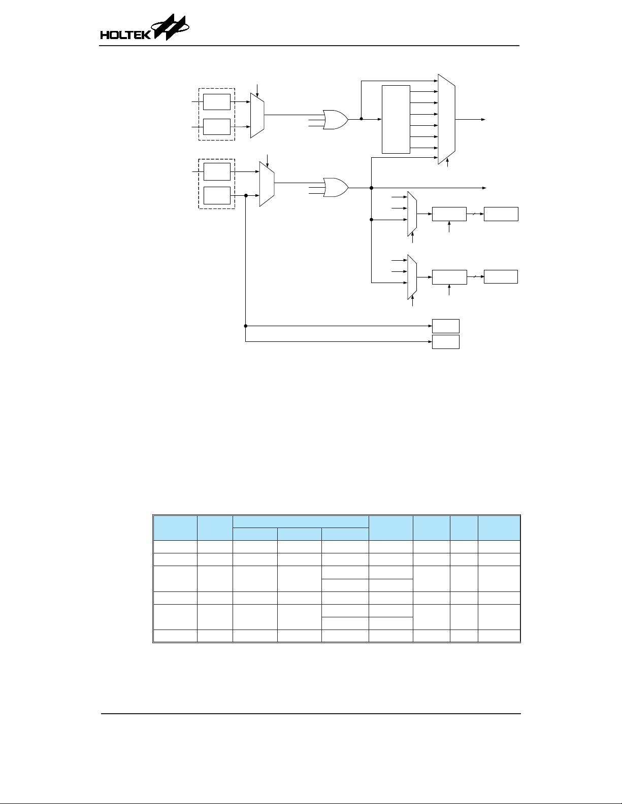
HIRCEN
HXTEN
High Speed
Oscillators
HIRC
HXT
FHS
HT45F4050
A/D NFC Flash MCU
f
H
fH/2
/4
f
H
f
/8
H
/16
f
H
f
/32
H
f
/64
H
FSS
IDLE0
SLEEP
f
H
Prescaler
f
SYS
LXTEN
LXT
LIRC
Low Speed
Oscillators
Note: When the system clock source f
can be stopped to conserve the power or continue to oscillate to provide the clock source,
fH~fH/64, for peripheral circuit to use, which is determined by conguring the corresponding
high speed oscillator enable control bit.
System Operation Modes
There are six different modes of operation for the microcontroller, each one with its own special
characteristics and which can be chosen according to the specic performance and power requirements
of the application. There are two modes allowing normal operation of the microcontroller, the
NORMAL Mode and SLOW Mode. The remaining four modes, the SLEEP, IDLE0, IDLE1 and
IDLE2 Mode are used when the microcontroller CPU is switched off to conserve power.
Operation
Mode
NORMAL On x x 000~110 fH~fH/64 On On On
Slow On x x 111 f
IDLE0 Off 0 1
IDLE1 Off 1 1 xxx On On On On
IDLE 2 Off 1 0
SLEEP Off 0 0 xxx Off Off Off On/Off
Note: 1. The fH clock will be switched on or off by conguring the corresponding oscillator enable
2. The f
CPU
bit in the SLOW mode.
clock can be switched on or off which is controlled by the WDT function being
LIRC
enabled or disabled in the SLEEP mode.
f
LIRC
IDLE2
SLEEP
Device Clock Congurations
is switched to f
SYS
Related Register
FHIDEN FSIDEN CKS[2:0]
000~110 Off
111 On
000~110 On
111 Off
CKS2~CKS0
f
SUB
f
SYS
f
/4
SYS
f
SUB
f
SYS
f
/4
SYS
f
SUB
from fH, the high speed oscillation
SUB
f
SYS
SUB
fPSC0
CLKSEL0[1:0]
fPSC1
CLKSEL1[1:0]
f
LIRC
f
LIRC
On/Off
Prescaler 0
TB0 [2:0]
Prescaler 1
TB1 [2:0]
WDT
f
H
(1)
LVR
f
SUB
On On
f
Time Base 0
Time Base 1
f
Off On On
On Off On
"x ": Don’t care
SUB
LIRC
(2)
Rev. 1.00 46 September 11, 2018 Rev. 1.00 47 September 11, 2018
Page 47
HT45F4050
A/D NFC Flash MCU
NORMAL Mode
As the name suggests this is one of the main operating modes where the microcontroller has all of
its functions operational and where the system clock is provided by one of the high speed oscillators.
This mode operates allowing the microcontroller to operate normally with a clock source will come
from one of the high speed oscillators, either the HXT or HIRC oscillator. The high speed oscillator
will however first be divided by a ratio ranging from 1 to 64, the actual ratio being selected by
the CKS2~CKS0 bits in the SCC register. Although a high speed oscillator is used, running the
microcontroller at a divided clock ratio reduces the operating current.
SLOW Mode
This is also a mode where the microcontroller operates normally although now with a slower speed
clock source. The clock source used will be from f
LIRC or LXT oscillator.
SLEEP Mode
The SLEEP Mode is entered when an HALT instruction is executed and when the FHIDEN and
FSIDEN bit are low. In the SLEEP mode the CPU will be stopped and the f
peripheral functions will be stopped too. However the f
WDT function is enabled by the WDTC register.
SUB
. The f
LIRC
clock is derived from either the
SUB
clock provided to
SUB
clock can still continue to operate if the
IDLE0 Mode
The IDLE0 Mode is entered when an HALT instruction is executed and when the FHIDEN bit in the
SCC register is low and the FSIDEN bit in the SCC register is high. In the IDLE0 Mode the CPU will
be switched off but the low speed oscillator will be turned on to drive some peripheral functions.
IDLE1 Mode
The IDLE1 Mode is entered when an HALT instruction is executed and when the FHIDEN bit in the
SCC register is high and the FSIDEN bit in the SCC register is high. In the IDLE1 Mode the CPU
will be switched off but both the high and low speed oscillators will be turned on to provide a clock
source to keep some peripheral functions operational.
IDLE2 Mode
The IDLE2 Mode is entered when an HALT instruction is executed and when the FHIDEN bit in the
SCC register is high and the FSIDEN bit in the SCC register is low. In the IDLE2 Mode the CPU
will be switched off but the high speed oscillator will be turned on to provide a clock source to keep
some peripheral functions operational.
Control Register
The registers, SCC, HIRCC, HXTC and LXTC, are used to control the system clock and the
corresponding oscillator congurations.
Register
Name
SCC CKS2 CKS1 CKS0 — FHS FSS FHIDEN FSIDEN
HIRCC — — — — HIRC1 HIRC0 HIRCF HIRCEN
HXTC — — — — — HXTM HXTF HXTEN
LXTC — — — — — — LXTF LXTEN
Bit
7 6 5 4 3 2 1 0
System Operating Mode Control Registers List
Page 48

HT45F4050
A/D NFC Flash MCU
• SCC Register
Bit 7 6 5 4 3 2 1 0
Name CKS2 CKS1 CKS0 — FHS FSS FHIDEN FSIDEN
R/W R/W R/W R/W — R/W R/W R/W R/W
POR 0 0 0 — 0 0 0 0
Bit 7~5 CKS2~CKS0: System clock selection
000: f
H
001: fH/2
010: fH/4
011: fH/8
100: fH/16
101: fH/32
110: fH/64
111: f
SUB
These three bits are used to select which clock is used as the system clock source. In
addition to the system clock source directly derived from fH or f
of the high speed system oscillator can also be chosen as the system clock source.
Bit 4 Unimplemented, read as "0"
Bit 3 FHS: High Frequency clock selection
0: HIRC
1: HXT
Bit 2 FSS: Low Frequency clock selection
0: LIRC
1: LXT
Bit 1 FHIDEN: High Frequency oscillator control when CPU is switched off
0: Disable
1: Enable
This bit is used to control whether the high speed oscillator is activated or stopped
when the CPU is switched off by executing an "HALT" instruction.
Bit 0 FSIDEN: Low Frequency oscillator control when CPU is switched off
0: Disable
1: Enable
This bit is used to control whether the low speed oscillator is activated or stopped
when the CPU is switched off by executing an "HALT" instruction.
, a divided version
SUB
• HIRCC Register
Bit 7 6 5 4 3 2 1 0
Name — — — — HIRC1 HIRC0 HIRCF HIRCEN
R/W — — — — R/W R/W R R/W
POR — — — — 0 0 0 1
Bit 7~4 Unimplemented, read as "0"
Bit 3~2 HIRC1~HIRC0: HIRC frequency selection
00: 4MHz
01: 8MHz
10: 12MHz
11: 4MHz
When the HIRC oscillator is enabled or the HIRC frequency selection is changed
by application program, the clock frequency will automatically be changed after the
HIRCF ag is set to 1. It is recommended that the HIRC frequency selected by these
bits is the same as the frequency determined by the conguration option to ensure a
higer HIRC frequency accuracy spedied in the A.C. chanracteristics.
Rev. 1.00 48 September 11, 2018 Rev. 1.00 49 September 11, 2018
Page 49

HT45F4050
A/D NFC Flash MCU
Bit 1 HIRCF: HIRC oscillator stable ag
This bit is used to indicate whether the HIRC oscillator is stable or not. When the
HIRCEN bit is set to 1 to enable the HIRC oscillator or the HIRC frequency selection
is changed by application program, the HIRCF bit will rst be cleared to 0 and then
set to 1 after the HIRC oscillator is stable.
Bit 0 HIRCEN: HIRC oscillator enable control
• HXTC Register
Bit 7 6 5 4 3 2 1 0
Name — — — — — HXTM HXTF HXTEN
R/W — — — — — R/W R R/W
POR — — — — — 0 0 0
Bit 7~3 Unimplemented, read as "0"
Bit 2 HXTM: HXT mode selection
This bit is used to select the HXT oscillator operating mode. Note that this bit must
be properly congured before the HXT is enabled. When the OSC1 and OSC2 pins
are enabled and the HXTEN bit is set to 1 to enable the HXT oscillator, it is invalid to
change the value of this bit. Otherwise, this bit value can be changed with no operation
on the HXT function.
Bit 1 HXTF: HXT oscillator stable ag
This bit is used to indicate whether the HXT oscillator is stable or not. When the
HXTEN bit is set to 1 to enable the HXT oscillator, the HXTF bit will rst be cleared
to 0 and then set to 1 after the HXT oscillator is stable.
Bit 0 HXTEN: HXT oscillator enable control
0: HIRC unstable
1: HIRC stable
0: Disable
1: Enable
0: HXT frequency ≤ 10 MHz
1: HXT frequency > 10 MHz
0: HXT unstable
1: HXT stable
0: Disable
1: Enable
• LXTC Register
Bit 7 6 5 4 3 2 1 0
Name — — — — — — LXTF LXTEN
R/W — — — — — — R R/W
POR — — — — — — 0 0
Bit 7~2 Unimplemented, read as "0"
Bit 1 LXTF: LXT oscillator stable ag
0: LXT unstable
1: LXT stable
This bit is used to indicate whether the LXT oscillator is stable or not. When the
LXTEN bit is set to 1 to enable the LXT oscillator, the LXTF bit will rst be cleared
to 0 and then set to 1 after the LXT oscillator is stable.
Bit 0 LXTEN: LXT oscillator enable control
0: Disable
1: Enable
Page 50

Operating Mode Switching
The device can switch between operating modes dynamically allowing the user to select the best
performance/power ratio for the present task in hand. In this way microcontroller operations that
do not require high performance can be executed using slower clocks thus requiring less operating
current and prolonging battery life in portable applications.
In simple terms, Mode Switching between the NORMAL Mode and SLOW Mode is executed using
the CKS2~CKS0 bits in the SCC register while Mode Switching from the NORMAL/SLOW Modes
to the SLEEP/IDLE Modes is executed via the HALT instruction. When an HALT instruction is
executed, whether the device enters the IDLE Mode or the SLEEP Mode is determined by the
condition of the FHIDEN and FSIDEN bits in the SCC register.
HT45F4050
A/D NFC Flash MCU
SLEEP
HALT instruction executed
CPU stop
FHIDEN=0
FSIDEN=0
off
f
H
off
f
SUB
NORMAL
f
SYS=fH~fH
fHon
/64
CPU run
f
on
SYS
f
on
SUB
HALT instruction executed
IDLE2
CPU stop
FHIDEN=1
FSIDEN=0
on
f
H
off
f
SUB
SLOW
f
SYS=fSUB
f
on
SUB
CPU run
f
on
SYS
fHon/off
HALT instruction executed
IDLE1
CPU stop
FHIDEN=1
FSIDEN=1
on
f
H
on
f
SUB
HALT instruction executed
IDLE0
CPU stop
FHIDEN=0
FSIDEN=1
off
f
H
on
f
SUB
Rev. 1.00 50 September 11, 2018 Rev. 1.00 51 September 11, 2018
Page 51

HT45F4050
A/D NFC Flash MCU
NORMAL Mode to SLOW Mode Switching
When running in the NORMAL Mode, which uses the high speed system oscillator, and therefore
consumes more power, the system clock can switch to run in the SLOW Mode by set the CKS2~CKS0
bits to "111" in the SCC register. This will then use the low speed system oscillator which will
consume less power. Users may decide to do this for certain operations which do not require high
performance and can subsequently reduce power consumption.
The SLOW Mode is sourced from the LXT or LIRC oscillator determined by the FSS bit in the SCC
register and therefore requires this oscillator to be stable before full mode switching occurs.
NORMAL Mode
CKS2~CKS0 = 111
SLOW Mode
FHIDEN=0, FSIDEN=0
HALT instruction is executed
SLEEP Mode
FHIDEN=0, FSIDEN=1
HALT instruction is executed
IDLE0 Mode
FHIDEN=1, FSIDEN=1
HALT instruction is executed
FHIDEN=1, FSIDEN=0
HALT instruction is executed
IDLE2 Mode
IDLE1 Mode
Page 52

HT45F4050
A/D NFC Flash MCU
SLOW Mode to NORMAL Mode Switching
In SLOW mode the system clock is derived from f
NORMAL mode from f
, the CKS2~CKS0 bits should be set to "000" ~"110" and then the system
SUB
clock will respectively be switched to fH~ fH/64.
However, if fH is not used in SLOW mode and thus switched off, it will take some time to re-
oscillate and stabilise when switching to the NORMAL mode from the SLOW Mode. This is
monitored using the HXTF bit in the HXTC register or the HIRCF bit in the HIRCC register. The
time duration required for the high speed system oscillator stabilization is specified in the A.C.
characteristics.
FHIDEN=0, FSIDEN=0
HALT instruction is executed
FHIDEN=0, FSIDEN=1
HALT instruction is executed
. When system clock is switched back to the
SUB
SLOW Mode
CKS2~CKS0 = 000~110
NORMAL Mode
SLEEP Mode
IDLE0 Mode
FHIDEN=1, FSIDEN=1
HALT instruction is executed
IDLE1 Mode
FHIDEN=1, FSIDEN=0
HALT instruction is executed
IDLE2 Mode
Entering the SLEEP Mode
There is only one way for the device to enter the SLEEP Mode and that is to execute the "HALT"
instruction in the application program with both the FHIDEN and FSIDEN bits in the SCC register
equal to "0". In this mode all the clocks and functions will be switched off except the WDT function.
When this instruction is executed under the conditions described above, the following will occur:
• The system clock will be stopped and the application program will stop at the "HALT" instruction.
• The Data Memory contents and registers will maintain their present condition.
• The I/O ports will maintain their present conditions.
• In the status register, the Power Down ag PDF will be set, and WDT timeout ag TO will be cleared.
• The WDT will be cleared and resume counting if the WDT is enabled. If the WDT is disabled
then WDT will be cleared and stopped.
Rev. 1.00 52 September 11, 2018 Rev. 1.00 53 September 11, 2018
Page 53

HT45F4050
A/D NFC Flash MCU
Entering the IDLE0 Mode
There is only one way for the device to enter the IDLE0 Mode and that is to execute the "HALT"
instruction in the application program with the FHIDEN bit in the SCC register equal to "0" and the
FSIDEN bit in the SCC register equal to "1". When this instruction is executed under the conditions
described above, the following will occur:
• The fH clock will be stopped and the application program will stop at the "HALT" instruction, but
the f
clock will be on.
SUB
• The Data Memory contents and registers will maintain their present condition.
• The I/O ports will maintain their present conditions.
• In the status register, the Power Down ag PDF will be set, and WDT timeout ag TO will be cleared.
• The WDT will be cleared and resume counting if the WDT is enabled. If the WDT is disabled
then WDT will be cleared and stopped.
Entering the IDLE1 Mode
There is only one way for the device to enter the IDLE1 Mode and that is to execute the "HALT"
instruction in the application program with the FHIDEN bit in SCC register equal to "1" and the
FSIDEN bit in the SCC register equal to "1". When this instruction is executed under the conditions
described above, the following will occur:
• The fH and f
• The Data Memory contents and registers will maintain their present condition.
• The I/O ports will maintain their present conditions.
• In the status register, the Power Down ag PDF will be set, and WDT timeout ag TO will be cleared.
• The WDT will be cleared and resume counting as the WDT is enabled. If the WDT is disabled
then WDT will be cleared and stopped.
clocks will be on but the application program will stop at the "HALT" instruction.
SUB
Entering the IDLE2 Mode
There is only one way for the device to enter the IDLE2 Mode and that is to execute the "HALT"
instruction in the application program with the FHIDEN bit in the SCC register equal to "1" and the
FSIDEN bit in SCC register equal to "0". When this instruction is executed under the conditions
described above, the following will occur:
• The fH clock will be on but the f
clock will be off and the application program will stop at the
SUB
"HALT" instruction.
• The Data Memory contents and registers will maintain their present condition.
• The I/O ports will maintain their present conditions.
• In the status register, the Power Down ag PDF will be set, and WDT timeout ag TO will be cleared.
• The WDT will be cleared and resume counting if the WDT is enabled. If the WDT is disabled
then WDT will be cleared and stopped.
Page 54

Standby Current Considerations
As the main reason for entering the SLEEP or IDLE Mode is to keep the current consumption of the
device to as low a value as possible, perhaps only in the order of several micro-amps except in the
IDLE1 and IDLE2 Mode, there are other considerations which must also be taken into account by
the circuit designer if the power consumption is to be minimised. Special attention must be made
to the I/O pins on the device. All high-impedance input pins must be connected to either a xed
high or low level as any oating input pins could create internal oscillations and result in increased
current consumption. These must either be setup as outputs or if setup as inputs must have pull-high
resistors connected.
Care must also be taken with the loads, which are connected to I/O pins, which are setup as outputs.
These should be placed in a condition in which minimum current is drawn or connected only to
external circuits that do not draw current, such as other CMOS inputs. Also note that additional
standby current will also be required if the LXT or LIRC oscillator has enabled.
In the IDLE1 and IDLE2 Mode the high speed oscillator is on, if the peripheral function clock
source is derived from the high speed oscillator, the additional standby current will also be perhaps
in the order of several hundred micro-amps.
Wake-up
To minimise power consumption the device can enter the SLEEP or any IDLE Mode, where the
CPU will be switched off. However, when the device is woken up again, it will take a considerable
time for the original system oscillator to restart, stablise and allow normal operation to resume.
After the system enters the SLEEP or IDLE Mode, it can be woken up from one of various sources
listed as follows:
• An external falling edge on Port A
• An external reset
• A system interrupt
• A WDT overow
If the system is woken up by an external reset, the device will experience a full system reset,
however, if the device is woken up by a WDT overow, a Watchdog Timer reset will be initiated.
Although both of these wake-up methods will initiate a reset operation, the actual source of the
wake-up can be determined by examining the TO and PDF flags. The PDF flag is cleared by a
system power-up or executing the clear Watchdog Timer instructions and is set when executing the
"HALT" instruction. The TO ag is set if a WDT time-out occurs and causes a wake-up that only
resets the Program Counter and Stack Pointer, other ags remain in their original status.
Each pin on Port A can be setup using the PAWU register to permit a negative transition on the pin
to wake up the system. When a Port A pin wake-up occurs, the program will resume execution at
the instruction following the "HALT" instruction. If the system is woken up by an interrupt, then
two possible situations may occur. The rst is where the related interrupt is disabled or the interrupt
is enabled but the stack is full, in which case the program will resume execution at the instruction
following the "HALT" instruction. In this situation, the interrupt which woke up the device will
not be immediately serviced, but wukk rather be serviced later when the related interrupt is nally
enabled or when a stack level becomes free. The other situation is where the related interrupt is
enabled and the stack is not full, in which case the regular interrupt response takes place. If an
interrupt request ag is set high before entering the SLEEP or IDLE Mode, the wake-up function of
the related interrupt will be disabled.
HT45F4050
A/D NFC Flash MCU
Rev. 1.00 54 September 11, 2018 Rev. 1.00 55 September 11, 2018
Page 55

HT45F4050
A/D NFC Flash MCU
Watchdog Timer
The Watchdog Timer is provided to prevent program malfunctions or sequences from jumping to
unknown locations, due to certain uncontrollable external events such as electrical noise.
Watchdog Timer Clock Source
The Watchdog Timer clock source is sourced from the LIRC oscillator. The LIRC internal oscillator
has an approximate frequency of 32kHz and this specied internal clock period can vary with VDD,
temperature and process variations. The Watchdog Timer source clock is then subdivided by a ratio
of 28 to 218 to give longer timeouts, the actual value being chosen using the WS2~WS0 bits in the
WDTC register.
Watchdog Timer Control Register
A single register, WDTC, controls the required timeout period as well as the enable/disable
operation. This register controls the overall operation of the Watchdog Timer.
• WDTC Register
Bit 7 6 5 4 3 2 1 0
Name WE4 WE3 WE2 WE1 WE0 WS2 WS1 WS0
R/W R/W R/W R/W R/W R/W R/W R/W R/W
POR 0 1 0 1 0 0 1 1
Bit 7~3 WE4~WE0: WDT function software control
10101: Disable
01010: Enable
Other values: Reset MCU
When these bits are changed by the environmental noise or software setting to reset
the microcontroller, the reset operation will be activated after a delay time, t
the WRF bit in the RSTFC register will be set to 1.
Bit 2~0 WS2~WS0: WDT time-out period selection
000: 28/f
001: 210/f
010: 212/f
011: 214/f
100: 215/f
101: 216/f
110: 217/f
111: 218/f
LIRC
LIRC
LIRC
LIRC
LIRC
LIRC
LIRC
LIRC
These three bits determine the division ratio of the Watchdog Timer source clock,
which in turn determines the timeout period.
• RSTFC Register
Bit 7 6 5 4 3 2 1 0
Name — — — — RSTF LVRF LRF WRF
R/W — — — — R/W R/W R/W R/W
POR — — — — 0 x 0 0
Bit 7~4 Unimplemented, read as "0"
Bit 3 RSTF: Reset control register software reset ag
Refer to the RES Pin Reset section.
Bit 2 LVRF: LVR function reset ag
Refer to the Low Voltage Reset section.
, and
SRESET
"x": unknown
Page 56

Bit 1 LRF: LVR control register software reset ag
Refer to the Low Voltage Reset section.
Bit 0 WRF: WDT control register software reset ag
0: Not occurred
1: Occurred
This bit is set to 1 by the WDT control register software reset and cleared by the application
program. Note that this bit can only be cleared to 0 by the application program.
Watchdog Timer Operation
The Watchdog Timer operates by providing a device reset when its timer overows. This means
that in the application program and during normal operation the user has to strategically clear the
Watchdog Timer before it overows to prevent the Watchdog Timer from executing a reset. This is
done using the clear watchdog instruction. If the program malfunctions for whatever reason, jumps
to an unknown location, or enters an endless loop, the clear instruction will not be executed in the
correct manner, in which case the Watchdog Timer will overow and reset the device. With regard to
the Watchdog Timer enable/disable function, there are ve bits, WE4~WE0, in the WDTC register
to offer additional enable/disable and reset control of the Watchdog Timer. The WDT function
will be disabled when the WE4~WE0 bits are set to a value of 10101B. The WDT function will be
enabled if the WE4~WE0 bits value is equal to 01010B. If the WE4~WE0 bits are set to any other
values other than 01010B and 10101B, it will reset the device after a delay time, t
on these bits will have the value of 01010B.
Under normal program operation, a Watchdog Timer time-out will initialise a device reset and set
the status bit TO. However, if the system is in the SLEEP or IDLE Mode, when a Watchdog Timer
time-out occurs, the TO bit in the status register will be set and only the Program Counter and Stack
Pointer will be reset. Four methods can be adopted to clear the contents of the Watchdog Timer. The
rst is a WDTC software reset, which means a certain value except 01010B and 10101B written into
the WE4~WE0 bits, the second is using the Watchdog Timer software clear instruction, the third
is via a HALT instruction. The last is an external hardware reset, which means a low level on the
external reset pin if the external reset pin function is selected by conguring the RSTC register.
There is only one method of using software instruction to clear the Watchdog Timer. That is to use
the single "CLR WDT" instruction to clear the WDT.
The maximum time out period is when the 218 division ratio is selected. As an example, with a
32kHz LIRC oscillator as its source clock, this will give a maximum watchdog period of around 8
seconds for the 218 division ratio, and a minimum timeout of 8ms for the 28 division ration.
A/D NFC Flash MCU
WE4~WE0 Bits WDT Function
10101B Disable
01010B Enable
Any other value Reset MCU
Watchdog Timer Enable/Disable Control
HT45F4050
. After power
SRESET
WDTC
Register
Rev. 1.00 56 September 11, 2018 Rev. 1.00 57 September 11, 2018
WE4~WE0 bits
“CLR WDT” Instruction
“HALT” Instruction
RES pin reset
LIRC
CLR
f
LIRC
8-stage Divider WDT Prescaler
Watchdog Timer
f
LIRC
Reset MCU
8
/2
8-to-1 MUXWS2~WS0
WDT Time-out
8
/f
~ 218/f
(2
LIRC
LIRC
)
Page 57

HT45F4050
A/D NFC Flash MCU
Reset and Initialisation
A reset function is a fundamental part of any microcontroller ensuring that the device can be set
to some predetermined condition irrespective of outside parameters. The most important reset
condition is after power is rst applied to the microcontroller. In this case, internal circuitry will
ensure that the microcontroller, after a short delay, will be in a well-defined state and ready to
execute the rst program instruction. After this power-on reset, certain important internal registers
will be set to dened states before the program commences. One of these registers is the Program
Counter, which will be reset to zero forcing the microcontroller to begin program execution from the
lowest Program Memory address.
In addition to the power-on reset, situations may arise where it is necessary to forcefully apply
a reset condition when the device is running. One example of this is where after power has been
applied and the device is already running, the RES line is forcefully pulled low. In such a case,
known as a normal operation reset, some of the registers remain unchanged allowing the device to
proceed with normal operation after the reset line is allowed to return high.
Another reset exists in the form of a Low Voltage Reset, LVR, where a full reset, similar to the RES
reset is implemented in situations where the power supply voltage falls below a certain threshold.
Another type of reset is when the Watchdog Timer overflows and resets the microcontroller. All
types of reset operations result in different register conditions being setup.
Reset Functions
There are several ways in which a microcontroller reset can occur, through events occurring both
internally and externally.
Power-on Reset
The most fundamental and unavoidable reset is the one that occurs after power is rst applied to
the microcontroller. As well as ensuring that the Program Memory begins execution from the rst
memory address, a power-on reset also ensures that certain other registers are preset to known
conditions. All the I/O port and port control registers will power up in a high condition ensuring that
all I/O ports will be rst set to inputs.
RES Pin Reset
Although the microcontroller has an internal RC reset function, if the VDD power supply rise time
is not fast enough or does not stabilise quickly at power-on, the internal reset function may be
incapable of providing proper reset operation. For this reason it is recommended that an external
RC network is connected to the RES pin, whose additional time delay will ensure that the RES pin
remains low for an extended period to allow the power supply to stabilise. During this time delay,
normal operation of the microcontroller will be inhibited. After the RES line reaches a certain
voltage value, the reset delay time t
microcontroller will begin normal operation. The abbreviation SST in the gures stands for System
Start-up Timer.
VDD
RES
Internal Reset
Power-On Reset Timing Chart
0.9V
DD
t
RSTD+tSST
is invoked to provide an extra delay time after which the
RSTD
Page 58
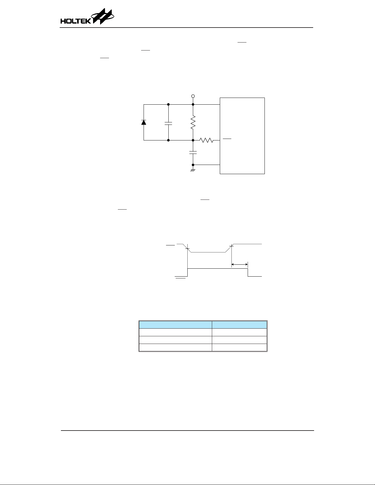
HT45F4050
A/D NFC Flash MCU
For most applications a resistor connected between VDD and the RES pin and a capacitor connected
between VSS and the RES pin will provide a suitable external reset circuit. Any wiring connected to
the RES pin should be kept as short as possible to minimise any stray noise interference.
For applications that operate within an environment where more noise is present the Enhanced Reset
Circuit shown is recommended.
V
DD
VDD
1N4148*
0.01µF**
0.1µF~1µF
10kΩ~
100kΩ
300Ω*
RES
VSS
Note: * It is recommended that this component is added for added ESD protection.
** It is recommended that this component is added in environments where power line noise is
signicant.
External RES Circuit
Pulling the RES Pin low using external hardware will also execute a device reset. In this case, as in
the case of other resets, the Program Counter will reset to zero and program execution initiated from
this point.
0.9V
DD
t
RSTD+tSST
RES
Internal Reset
0.4V
DD
RES Reset Timing Chart
There is an internal reset control register, RSTC, which is used to provide a reset when the device
operates abnormally due to the environmental noise interference. If the content of the RSTC register
is set to any value other than 01010101B or 10101010B, it will reset the device after a delay time,
t
. After power on the register will have a value of 01010101B.
SRESET
RSTC7 ~ RSTC0 Bits Reset Function
01010101B I/O
10101010B RES
Any other value Reset MCU
Internal Reset Function Control
Rev. 1.00 58 September 11, 2018 Rev. 1.00 59 September 11, 2018
Page 59
HT45F4050
A/D NFC Flash MCU
• RSTC Register
Bit 7 6 5 4 3 2 1 0
Name RSTC7 RSTC6 RSTC5 RSTC4 RSTC3 RSTC2 RSTC1 RSTC0
R/W R/W R/W R/W R/W R/W R/W R/W R/W
POR 0 1 0 1 0 1 0 1
Bit 7~0 RSTC7~RSTC0: Reset function control
If these bits are changed due to adverse environmental conditions, the microcontroller
will be reset. The reset operation will be activated after a delay time, t
RSTF bit in the RSTFC register will be set to 1.
All resets will reset this register to POR value except the WDT time out hardware
warm reset. Note that when if this register is set to 10101010B to select the RES pin
function, this conguration has higher priority than other related pin-shared controls.
• RSTFC Register
Bit 7 6 5 4 3 2 1 0
Name — — — — RSTF LVRF LRF WRF
R/W — — — — R/W R/W R/W R/W
POR — — — — 0 x 0 0
Bit 7~4 Unimplemented, read as "0"
Bit 3 RSTF: Reset control register software reset ag
This bit is set to 1 by the RSTC control register software reset and cleared by the
application program. Note that this bit can only be cleared to 0 by the application
program.
Bit 2 LVRF: LVR function reset ag
Refer to the Low Voltage Reset section.
Bit 1 LRF: LVR control register software reset ag
Refer to the Low Voltage Reset section.
Bit 0 WRF: WDT control register software reset ag
Refer to the Watchdog Timer Control Register section.
01010101: PB5
10101010: RES pin
Other values: Reset MCU
0: Not occurred
1: Occurred
, and the
SRESET
"x": unknown
Low Voltage Reset – LVR
The microcontroller contains a low voltage reset circuit in order to monitor the supply voltage of the
device. The LVR function is always enabled with a specic LVR voltage V
of the device drops to within a range of 0.9V~V
such as might occur when changing the battery,
LVR
. If the supply voltage
LVR
the LVR will automatically reset the device internally and the LVRF bit in the RSTFC register will
also be set to 1. For a valid LVR signal, a low supply voltage, i.e., a voltage in the range between
0.9V~V
must exist for a time greater than that specied by t
LVR
in the LVD & LVR Electrical
LVR
Characteristics. If the low supply voltage state does not exceed this value, the LVR will ignore the
low supply voltage and will not perform a reset function. The actual V
value can be selected by
LVR
the LVS bits in the LVRC register. If the LVS7~LVS0 bits are changed to some certain values by
the environmental noise or software setting, the LVR will reset the device after a delay time, t
When this happens, the LRF bit in the RSTFC register will be set to 1. After power on the register
will have the value of 01100110B. Note that the LVR function will be automatically disabled when
the device enters the IDLE or SLEEP mode.
SRESET
.
Page 60

HT45F4050
A/D NFC Flash MCU
LVR
t
+ t
RSTD
SST
Internal Reset
Low Voltage Reset Timing Chart
• LVRC Register
Bit 7 6 5 4 3 2 1 0
Name LVS7 LVS6 LVS5 LVS4 LVS3 LVS2 LVS1 LVS0
R/W R/W R/W R/W R/W R/W R/W R/W R/W
POR 0 1 1 0 0 1 1 0
Bit 7~0 LVS7~LVS0: LVR voltage select
01100110: 1.65V
01010101: 1.90V
00110011: 2.55V
10011001: 3.15V
10101010: 3.80V
11110000: LVR disable
Any other value: Generates a MCU reset – register is reset to POR value
When an actual low voltage condition occurs, as specied by one of the ve dened
LVR voltage values above, an MCU reset will be generated. The reset operation
will be activated after the low voltage condition keeps more than a t
situation the register contents will remain the same after such a reset occurs.
Any register value, other than the ve dened LVR values above, will also result in the
generation of an MCU reset. The reset operation will be activated after a delay time,
t
. However in this situation the register contents will be reset to the POR value.
SRESET
LVR
time. In this
• RSTFC Register
Bit 7 6 5 4 3 2 1 0
Name — — — — RSTF LVRF LRF WRF
R/W — — — — R/W R/W R/W R/W
POR — — — — 0 x 0 0
Bit 7~4 Unimplemented, read as "0"
Bit 3 RSTF: Reset control register software reset ag
Refer to the RES Pin Reset section.
Bit 2 LVRF: LVR function reset ag
0: Not occurred
1: Occurred
This bit is set to 1 when a specic low voltage reset condition occurs. Note that this bit
can only be cleared to 0 by the application program.
Bit 1 LRF: LVR control register software reset ag
0: Not occurred
1: Occurred
This bit is set to 1 by the LVRC control register contains any undened LVR voltage
register values. This in effect acts like a software-reset function. Note that this bit can
only be cleared to 0 by the application program.
Bit 0 WRF: WDT control register software reset ag
Refer to the Watchdog Timer Control Register section.
"x": unknown
Rev. 1.00 60 September 11, 2018 Rev. 1.00 61 September 11, 2018
Page 61
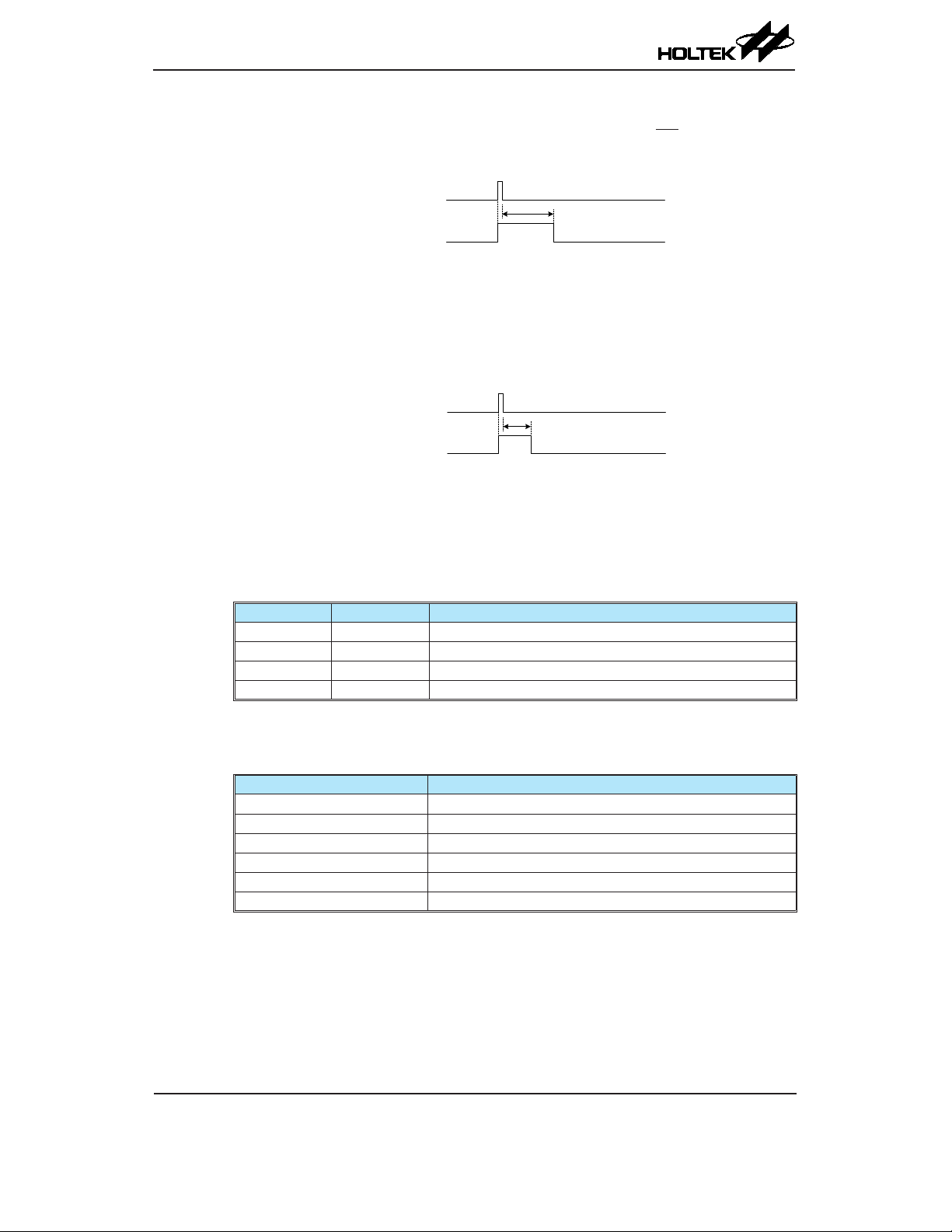
HT45F4050
A/D NFC Flash MCU
Watchdog Time-out Reset during Normal Operation
The Watchdog time-out Reset during normal operation is the same as the RES reset except that the
Watchdog time-out ag TO will be set to "1".
Watchdog Time-out Reset during SLEEP or IDLE Mode
The Watchdog time-out Reset during SLEEP or IDLE Mode is a little different from other kinds
of reset. Most of the conditions remain unchanged except that the Program Counter and the Stack
Pointer will be cleared to "0" and the TO ag will be set to "1". Refer to the A.C. Characteristics for
t
details.
SST
WDT Time-out
t
+ t
RSTD
SST
Internal Reset
WDT Time-out Reset during Normal Operation Timing Chart
WDT Time-out
t
SST
Internal Reset
WDT Time-out Reset during SLEEP or IDLE Timing Chart
Reset Initial Conditions
The different types of reset described affect the reset ags in different ways. These ags, known
as PDF and TO are located in the status register and are controlled by various microcontroller
operations, such as the SLEEP or IDLE Mode function or Watchdog Timer. The reset flags are
shown in the table:
TO PDF Reset Conditions
0 0 Power-on reset
u u RES or LVR reset during Normal or SLOW Mode operation
1 u WDT time-out reset during Normal or SLOW Mode operation
1 1 WDT time-out reset during IDLE or SLEEP Mode operation
Note: "u" stands for unchanged
The following table indicates the way in which the various components of the microcontroller are
affected after a power-on reset occurs.
Item Condition after Reset
Program Counter Reset to zero
Interrupts All interrupts will be disabled
WDT,Time Base Clear after reset, WDT begins counting
Timer Modules Timer Modules will be turned off
Input/Output Ports I/O ports will be setup as inputs
Stack Pointer Stack Pointer will point to the top of the stack
The different kinds of resets all affect the internal registers of the microcontroller in different ways.
To ensure reliable continuation of normal program execution after a reset occurs, it is important to
know what condition the microcontroller is in after a particular reset occurs. The following table
describes how each type of reset affects each of the microcontroller internal registers.
Page 62

HT45F4050
A/D NFC Flash MCU
Register Power On Reset
IAR0 0000 0000 0000 0000 0000 0000 0000 0000 uuuu uuuu
MP0 0000 0000 0000 0000 0000 0000 0000 0000 uuuu uuuu
IAR1 0000 0000 0000 0000 0000 0000 0000 0000 uuuu uuuu
MP1L 0000 0000 0000 0000 0000 0000 0000 0000 uuuu uuuu
MP1H 0000 0000 0000 0000 0000 0000 0000 0000 uuuu uuuu
ACC xxxx xxxx uuuu uuuu uuuu uuuu uuuu uuuu uuuu uuuu
PCL 0000 0000 0000 0000 0000 0000 0000 0000 0000 0000
TBLP xxxx xxxx uuuu uuuu uuuu uuuu uuuu uuuu uuuu uuuu
TBLH xxxx xxxx uuuu uuuu uuuu uuuu uuuu uuuu uuuu uuuu
TBHP ---x xxxx ---u uuuu ---u uuuu ---u uuuu ---u uuuu
STATUS xx00 xxxx uuuu uuuu uuuu uuuu xx1u uuuu uu11 uuuu
IAR2 0000 0000 0000 0000 0000 0000 0000 0000 uuuu uuuu
MP2L 0000 0000 0000 0000 0000 0000 0000 0000 uuuu uuuu
MP2H 0000 0000 0000 0000 0000 0000 0000 0000 uuuu uuuu
RSTFC ---- 0x00 ---- uuuu ---- u1 uu ---- uuuu ---- uuuu
INTC0 -000 0000 -000 0000 -000 0000 -000 0000 -uuu uuuu
INTC1 0000 0000 0000 0000 0000 0000 0000 0000 uuuu uuuu
INTC2 0000 0000 0000 0000 0000 0000 0000 0000 uuuu uuuu
INTC3 ---0 ---0 ---0 ---0 ---0 ---0 ---0 ---0 ---u ---u
PA 1111 1111 1111 1111 1111 1111 1111 1111 uuuu uuuu
PAC 1111 1111 1111 1111 1111 1111 1111 1111 uuuu uuuu
PAPU 0000 0000 0000 0000 0000 0000 0000 0000 uuuu uuuu
PAWU 0000 0000 0000 0000 0000 0000 0000 0000 uuuu uuuu
PB 1111 1111 1111 1111 1111 1111 1111 1111 uuuu uuuu
PBC 1111 1111 1111 1111 1111 1111 1111 1111 uuuu uuuu
PBPU 0000 0000 0000 0000 0000 0000 0000 0000 uuuu uuuu
PC 1111 1111 1111 1111 1111 1111 1111 1111 uuuu uuuu
PCC 1111 1111 1111 1111 1111 1111 1111 1111 uuuu uuuu
PCPU 0000 0000 0000 0000 0000 0000 0000 0000 uuuu uuuu
PD ---- 1111 ---- 1111 ---- 1111 ---- 1111 ---- uuuu
PDC ---- 1111 ---- 1111 ---- 1111 ---- 1111 ---- uuuu
PDPU ---- 0000 ---- 0000 ---- 0000 ---- 0000 ---- uuuu
PE ---1 1111 ---1 1111 ---1 1111 ---1 1111 ---u uuuu
PEC ---1 1111 ---1 1111 ---1 1111 ---1 1111 ---u uuuu
PEPU ---0 0000 ---0 0000 ---0 0000 ---0 0000 ---u uuuu
PF 1111 1111 1111 1111 1111 1111 1111 1111 uuuu uuuu
PFC 1111 1111 1111 1111 1111 1111 1111 1111 uuuu uuuu
PFPU 0000 0000 0000 0000 0000 0000 0000 0000 uuuu uuuu
RSTC 0101 0101 0101 0101 0101 0101 0101 0101 uuuu uuuu
VBGRC ---- ---0 ---- ---0 ---- ---0 ---- ---0 ---- ---u
MFI0 --00 --00 --00 --00 --00 --00 --00 --00 --uu --uu
MFI1 0000 0000 0000 0000 0000 0000 0000 0000 uuuu uuuu
MFI2 --00 --00 --00 --00 --00 --00 --00 --00 --uu --uu
INTEG ---- 0000 ---- 0000 ---- 0000 ---- 0000 ---- uuuu
PMPS ---- --00 ---- --00 ---- --00 ---- --00 ---- --uu
SCC 000- 0000 000- 0000 000- 0000 000- 0000 uuu- uuuu
HIRCC ---- 0001 ---- 0001 ---- 0001 ---- 0001 ---- uuuu
RES Reset
(Normal
Operation)
LVR Reset
(Normal
Operation)
WDT Time-out
(Normal
Operation)
WDT Time-out
(IDLE/SLEEP)
Rev. 1.00 62 September 11, 2018 Rev. 1.00 63 September 11, 2018
Page 63
HT45F4050
A/D NFC Flash MCU
Register Power On Reset
HXTC ---- -000 ---- -000 ---- -000 ---- -000 ---- -uuu
LXTC ---- --00 ---- --00 ---- --00 ---- --00 ---- --uu
WDTC 0101 0011 0101 0011 0101 0011 0101 0011 uuuu uuuu
LVRC 0110 0110 0110 0110 0110 0110 0110 0110 uuuu uuuu
LVDC --00 0000 --00 0000 --00 0000 --00 0000 --uu uuuu
LVPUC ---- ---0 ---- ---0 ---- ---0 ---- ---0 ---- ---u
CMPC -000 00-- -000 00-- -000 00-- -000 00-- -uuu uu--
CMPVOS -001 0000 -001 0000 -001 0000 -001 0000 -uuu uuuu
CTMC0 0000 0--- 0000 0--- 0000 0--- 0000 0--- uuuu u---
CTMC1 0000 0000 0000 0000 0000 0000 0000 0000 uuuu uuuu
CTMDL 0000 0000 0000 0000 0000 0000 0000 0000 uuuu uuuu
CTMDH 0000 0000 0000 0000 0000 0000 0000 0000 uuuu uuuu
CTMAL 0000 0000 0000 0000 0000 0000 0000 0000 uuuu uuuu
CTMAH 0000 0000 0000 0000 0000 0000 0000 0000 uuuu uuuu
CTMRP 0000 0000 0000 0000 0000 0000 0000 0000 uuuu uuuu
EEA --00 0000 --00 0000 --00 0000 --00 0000 --uu uuuu
EED 0000 0000 0000 0000 0000 0000 0000 0000 uuuu uuuu
PTMC0 0000 0--- 0000 0--- 0000 0--- 0000 0--- uuuu u---
PTMC1 0000 0000 0000 0000 0000 0000 0000 0000 uuuu uuuu
PTMDL 0000 0000 0000 0000 0000 0000 0000 0000 uuuu uuuu
PTMDH ---- --00 ---- --00 ---- --00 ---- --00 ---- --uu
PTMAL 0000 0000 0000 0000 0000 0000 0000 0000 uuuu uuuu
PTMAH ---- --00 ---- --00 ---- --00 ---- --00 ---- --uu
PTMRPL 0000 0000 0000 0000 0000 0000 0000 0000 uuuu uuuu
PTMRPH ---- --00 ---- --00 ---- --00 ---- --00 ---- --uu
STMC0 0000 0--- 0000 0--- 0000 0--- 0000 0--- uuuu u---
STMC1 0000 0000 0000 0000 0000 0000 0000 0000 uuuu uuuu
STMDL 0000 0000 0000 0000 0000 0000 0000 0000 uuuu uuuu
STMDH 0000 0000 0000 0000 0000 0000 0000 0000 uuuu uuuu
STMAL 0000 0000 0000 0000 0000 0000 0000 0000 uuuu uuuu
STMAH 0000 0000 0000 0000 0000 0000 0000 0000 uuuu uuuu
STMRP 0000 0000 0000 0000 0000 0000 0000 0000 uuuu uuuu
SLEDC0 0000 0000 0000 0000 0000 0000 0000 0000 uuuu uuuu
SLEDC1 --00 0000 --00 0000 --00 0000 --00 0000 --uu uuuu
SLEDC2 0000 0000 0000 0000 0000 0000 0000 0000 uuuu uuuu
TB0C 0--- -000 0--- -000 0--- -000 0--- -000 u--- -uuu
TB1C 0--- -000 0--- -000 0--- -000 0--- -000 u--- -uuu
PSC0R ---- --00 ---- --00 ---- --00 ---- --00 ---- --uu
PSC1R ---- --00 ---- --00 ---- --00 ---- --00 ---- --uu
SADOL xxxx ---- xxxx ---- xxxx ---- xxxx ----
SADOH xxxx xxxx xxxx xxxx xxxx xxxx xxxx xxxx
RES Reset
(Normal
Operation)
LVR Reset
(Normal
Operation)
WDT Time-out
(Normal
Operation)
WDT Time-out
(IDLE/SLEEP)
uuuu ----
(ADRFS=0)
uuuu uuuu
(ADRFS=1)
uuuu uuuu
(ADRFS=0)
---- uuuu
(ADRFS=1)
Page 64

HT45F4050
A/D NFC Flash MCU
Register Power On Reset
SADC0 0000 0000 0000 0000 0000 0000 0000 0000 uuuu uuuu
SADC1 0000 -000 0000 -000 0000 -000 0000 -000 uuuu -uuu
SADC2 0-00 0000 0-00 0000 0-00 0000 0-00 0000 u-uu uuuu
SIMC0 111- 0000 111- 0000 111- 0000 111- 0000 uuu- uuuu
SIMC1 1000 0001 1000 0001 1000 0001 1000 0001 uuuu uuuu
SIMD xxxx xxxx xxxx xxxx xxxx xxxx xxxx xxxx uuuu uuuu
SIMA/SIMC2 0000 0000 0000 0000 0000 0000 0000 0000 uuuu uuuu
SIMTOC 0000 0000 0000 0000 0000 0000 0000 0000 uuuu uuuu
SCOMC -000 ---- -000 ---- -000 ---- -000 ---- -uuu ----
USR 0000 1011 0000 1011 0000 1011 0000 1011 uuuu uuuu
UCR1 0000 00x0 0000 00x0 0000 00x0 0000 00x0 uuuu uuuu
UCR2 0000 0000 0000 0000 0000 0000 0000 0000 uuuu uuuu
TXR_RXR xxxx xxxx xxxx xxxx xxxx xxxx xxxx xxxx uuuu uuuu
BRG xxxx xxxx xxxx xxxx xxxx xxxx xxxx xxxx uuuu uuuu
IFS0 0000 0000 0000 0000 0000 0000 0000 0000 uuuu uuuu
IFS1 ---- --00 ---- --00 ---- --00 ---- --00 ---- --uu
PAS0 0000 0000 0000 0000 0000 0000 0000 0000 uuuu uuuu
PAS1 0000 0000 0000 0000 0000 0000 0000 0000 uuuu uuuu
PBS0 0000 0000 0000 0000 0000 0000 0000 0000 uuuu uuuu
PBS1 0000 0000 0000 0000 0000 0000 0000 0000 uuuu uuuu
PCS0 0000 0000 0000 0000 0000 0000 0000 0000 uuuu uuuu
PCS1 0000 0000 0000 0000 0000 0000 0000 0000 uuuu uuuu
PDS0 0000 0000 0000 0000 0000 0000 0000 0000 uuuu uuuu
PES0 0000 0000 0000 0000 0000 0000 0000 0000 uuuu uuuu
PES1 ---- --00 ---- --00 ---- --00 ---- --00 ---- --uu
PFS0 0000 0000 0000 0000 0000 0000 0000 0000 uuuu uuuu
PFS1 0000 0000 0000 0000 0000 0000 0000 0000 uuuu uuuu
NFCCTRL ---- 0000 ---- 0000 ---- 0000 ---- 0000 ---- uuuu
NFCEEC --00 0000 --00 0000 --00 0000 --00 0000 --uu uuuu
NFC_INTE 0000 0000 0000 0000 0000 0000 0000 0000 uuuu uuuu
NFC_INTF 0000 0000 0000 0000 0000 0000 0000 0000 uuuu uuuu
NFC_STATUS ---- 0000 ---- 0000 ---- 0000 ---- 0000 ---- uuuu
NFCEEA -000 0000 -000 0000 -000 0000 -000 0000 -uuu uuuu
NFCEED0 0000 0000 0000 0000 0000 0000 0000 0000 uuuu uuuu
NFCEED1 0000 0000 0000 0000 0000 0000 0000 0000 uuuu uuuu
NFCEED2 0000 0000 0000 0000 0000 0000 0000 0000 uuuu uuuu
NFCEED3 0000 0000 0000 0000 0000 0000 0000 0000 uuuu uuuu
NFCWRA -000 0000 -000 0000 -000 0000 -000 0000 -uuu uuuu
EEC ---- 0000 ---- 0000 ---- 0000 ---- 0000 ---- uuuu
RES Reset
(Normal
Operation)
LVR Reset
(Normal
Operation)
WDT Time-out
(Normal
Operation)
WDT Time-out
(IDLE/SLEEP)
Note: "u" stands for unchanged
"x" stands for unknown
"-" stands for Unimplemented
Rev. 1.00 64 September 11, 2018 Rev. 1.00 65 September 11, 2018
Page 65

HT45F4050
A/D NFC Flash MCU
Input/Output Ports
Holtek microcontrollers offer considerable exibility on their I/O ports. With the input or output
designation of every pin fully under user program control, pull-high selections for all ports and
wake-up selections on certain pins, the user is provided with an I/O structure to meet the needs of a
wide range of application possibilities.
The device provides bidirectional input/output lines labeled with port names PA~PF. These I/O ports
are mapped to the RAM Data Memory with specific addresses as shown in the Special Purpose
Data Memory table. All of these I/O ports can be used for input and output operations. For input
operation, these ports are non-latching, which means the inputs must be ready at the T2 rising edge
of instruction "MOV A, [m]", where m denotes the port address. For output operation, all the data is
latched and remains unchanged until the output latch is rewritten.
Register
Name
PA PA7 PA6 PA5 PA 4 PA 3 PA2 PA 1 PA 0
PAC PAC7 PAC6 PAC5 PAC4 PAC3 PAC2 PAC1 PAC0
PAPU PAPU7 PAPU6 PAPU5 PAPU4 PAPU3 PAPU2 PAPU1 PAPU0
PAWU PAWU7 PAWU6 PAWU5 PAWU4 PAWU3 PAWU2 PAWU1 PAWU0
PB PB7 PB6 PB5 PB4 PB3 PB2 PB1 PB0
PBC PBC7 PBC6 PBC5 PBC4 PBC3 PBC2 PBC1 PBC0
PBPU PBPU7 PBPU6 PBPU5 PBPU4 PBPU3 PBPU2 PBPU1 PBPU0
PC PC7 PC6 PC5 PC4 PC3 PC2 PC1 PC0
PCC PCC7 PCC6 PCC5 PCC4 PCC3 PCC2 PCC1 PCC0
PCPU PCPU7 PCPU6 PCPU5 PCPU4 PCPU3 PCPU2 PCPU1 PCPU0
PD — — — — PD3 PD2 PD1 PD0
PDC — — — — PDC3 PDC2 PDC1 PDC0
PDPU — — — — PDPU3 PDPU2 PDPU1 PDPU0
PE — — — PE4 PE3 PE2 PE1 PE0
PEC — — — PEC4 PEC3 PEC2 PEC1 PEC0
PEPU — — — PEPU4 PEPU3 PEPU2 PEPU1 PEPU0
PF PF7 PF6 PF5 PF4 PF3 PF2 PF1 PF0
PFC PFC7 PFC6 PFC5 PFC4 PFC3 PFC2 PFC1 PFC0
PFPU PFPU7 PFPU6 PFPU5 PFPU4 PFPU3 PFPU2 PFPU1 PFPU0
LVPUC — — — — — — — LVPU
Bit
7 6 5 4 3 2 1 0
"—": Unimplemented, read as "0"
I/O Logic Function Registers List
Page 66

Pull-high Resistors
Many product applications require pull-high resistors for their switch inputs usually requiring the
use of an external resistor. To eliminate the need for these external resistors, all I/O pins, when
congured as an input have the capability of being connected to an internal pull-high resistor. These
pull-high resistors are selected using the relevant pull-high control registers PAPU~PFPU and
LVPUC and are implemented using weak PMOS transistors. Note that the pull-high resistor can
be controlled by the relevant pull-high control registers only when the pin-shared functional pin is
selected as a logic input or NMOS output. Otherwise, the pull-high resistors can not be enabled.
• PxPU Register
Bit 7 6 5 4 3 2 1 0
Name PxPU7 PxPU6 PxPU5 PxPU4 PxPU3 PxPU2 PxPU1 PxPU0
R/W R/W R/W R/W R/W R/W R/W R/W R/W
POR 0 0 0 0 0 0 0 0
PxPUn: I/O Px.n Pin pull-high function control
0: Disable
1: Enable
The PxPUn bit is used to control the Px.n pin pull-high function. Here the "x" can be A, B, C, D, E
and F. However, the actual available bits for each I/O Port may be different.
HT45F4050
A/D NFC Flash MCU
• LV PUC Register
Bit 7 6 5 4 3 2 1 0
Name — — — — — — — LVPU
R/W — — — — — — — R/W
POR — — — — — — — 0
Bit 7~1 Unimplemented, read as "0"
Bit 0 LVPU: Low Voltage pull-high resistor control
Port A Wake-up
The HALT instruction forces the microcontroller into the SLEEP or IDLE Modes which preserves
power, a feature that is important for battery and other low-power applications. Various methods
exist to wake-up the microcontroller, one of which is to change the logic condition on one of the Port
A pins from high to low. This function is especially suitable for applications that can be woken up
via external switches. Each pin on Port A can be selected individually to have this wake-up feature
using the PAWU register. Note that the wake-up function can be controlled by the wake-up control
registers only when the pin-shared functional pin is selected as general purpose input/output and the
MCU enters the Power down mode.
0: All pin pull-high resistors are 30kΩ @ 5V
1: All pin pull-high resistors are 7.5kΩ @ 5V
Note that as the pull high resistors are formed using long PMOS transistors, lower
operating voltages will result in higher pull high resistor impedances. It is therefore
recommended that for lower voltage applications the lower pull high resistor value is
chosen.
Rev. 1.00 66 September 11, 2018 Rev. 1.00 67 September 11, 2018
Page 67

HT45F4050
A/D NFC Flash MCU
• PAWU Register
Bit 7 6 5 4 3 2 1 0
Name PAWU7 PAWU6 PAWU5 PAWU4 PAWU3 PAWU2 PAWU1 PAWU0
R/W R/W R/W R/W R/W R/W R/W R/W R/W
POR 0 0 0 0 0 0 0 0
Bit 7~0 PAWU7~PAWU0: PA7~PA0 wake-up function control
I/O Port Control Registers
Each I/O port has its own control register known as PAC~PFC, to control the input/output
configuration. With this control register, each CMOS output or input can be reconfigured
dynamically under software control. Each pin of the I/O ports is directly mapped to a bit in its
associated port control register. For the I/O pin to function as an input, the corresponding bit of the
control register must be written as a "1". This will then allow the logic state of the input pin to be
directly read by instructions. When the corresponding bit of the control register is written as a "0",
the I/O pin will be setup as a CMOS output. If the pin is currently setup as an output, instructions
can still be used to read the output register. However, it should be noted that the program will in fact
only read the status of the output data latch and not the actual logic status of the output pin.
0: Disable
1: Enable
• PxC Register
Bit 7 6 5 4 3 2 1 0
Name PxC7 PxC6 PxC5 PxC4 PxC3 PxC2 PxC1 PxC0
R/W R/W R/W R/W R/W R/W R/W R/W R/W
POR 1 1 1 1 1 1 1 1
PxCn: I/O Port x Pin type selection
0: Output
1: Input
The PxCn bit is used to control the pin type selection. Here the "x" can be A, B, C, D, E and F.
However, the actual available bits for each I/O Port may be different.
I/O Port Source Current Control
The device supports different source current driving capability for each I/O port. With the
corresponding selection registers, SLEDCn, specic I/O port can support four levels of the source
current driving capability. Users should refer to the D.C. characteristics section to select the desired
source current for different applications.
Register
Name
SLEDC0 SLEDC07 SLEDC06 SLEDC05 SLEDC04 SLEDC03 SLEDC02 SLEDC01 SLEDC00
SLEDC1 — — SLEDC15 SLEDC14 SLEDC13 SLEDC12 SLEDC11 SLEDC10
SLEDC2 SLEDC27 SLEDC26 SLEDC25 SLEDC24 SLEDC23 SLEDC22 SLEDC21 SLEDC20
7 6 5 4 3 2 1 0
I/O Port Source Current Control Registers List
Bit
Page 68

HT45F4050
A/D NFC Flash MCU
• SLEDC0 Register
Bit 7 6 5 4 3 2 1 0
Name SLEDC07 SLEDC06 SLEDC05 SLEDC04 SLEDC03 SLEDC02 SLEDC01 SLEDC00
R/W R/W R/W R/W R/W R/W R/W R/W R/W
POR 0 0 0 0 0 0 0 0
Bit 7~6 SLEDC07~SLEDC06: PB7~PB4 source current selection
00: Source current=Level 0 (min.)
01: Source current=Level 1
10: Source current=Level 2
11: Source current=Level 3 (max.)
Bit 5~4 SLEDC05~SLEDC04: PB3~PB0 source current selection
00: Source current=Level 0 (min.)
01: Source current=Level 1
10: Source current=Level 2
11: Source current=Level 3 (max.)
Bit 3~2 SLEDC03~SLEDC02: PA7~PA4 source current selection
00: Source current=Level 0 (min.)
01: Source current=Level 1
10: Source current=Level 2
11: Source current=Level 3 (max.)
Bit 1~0 SLEDC01~SLEDC00: PA3~PA0 source current selection
00: Source current=Level 0 (min.)
01: Source current=Level 1
10: Source current=Level 2
11: Source current=Level 3 (max.)
• SLEDC1 Register
Bit 7 6 5 4 3 2 1 0
Name — — SLEDC15 SLEDC14 SLEDC13 SLEDC12 SLEDC11 SLEDC10
R/W — — R/W R/W R/W R/W R/W R/W
POR — — 0 0 0 0 0 0
Bit 7~6 Unimplemented, read as "0"
Bit 5~4 SLEDC15~SLEDC14: PD3~PD0 source current selection
00: Source current=Level 0 (min.)
01: Source current=Level 1
10: Source current=Level 2
11: Source current=Level 3 (max.)
Bit 3~2 SLEDC13~SLEDC12: PC7~PC4 source current selection
00: Source current=Level 0 (min.)
01: Source current=Level 1
10: Source current=Level 2
11: Source current=Level 3 (max.)
Bit 1~0 SLEDC11~SLEDC10: PC3~PC0 source current selection
00: Source current=Level 0 (min.)
01: Source current=Level 1
10: Source current=Level 2
11: Source current=Level 3 (max.)
Rev. 1.00 68 September 11, 2018 Rev. 1.00 69 September 11, 2018
Page 69

HT45F4050
A/D NFC Flash MCU
• SLEDC2 Register
Bit 7 6 5 4 3 2 1 0
Name SLEDC27 SLEDC26 SLEDC25 SLEDC24 SLEDC23 SLEDC22 SLEDC21 SLEDC20
R/W R/W R/W R/W R/W R/W R/W R/W R/W
POR 0 0 0 0 0 0 0 0
Bit 7~6 SLEDC27~SLEDC26: PF7~PF4 source current selection
Bit 5~4 SLEDC25~SLEDC24: PF3~PF0 source current selection
Bit 3~2 SLEDC23~SLEDC22: PE4 source current selection
Bit 1~0 SLEDC21~SLEDC20: PE3~PE0 source current selection
00: Source current=Level 0 (min.)
01: Source current=Level 1
10: Source current=Level 2
11: Source current=Level 3 (max.)
00: Source current=Level 0 (min.)
01: Source current=Level 1
10: Source current=Level 2
11: Source current=Level 3 (max.)
00: Source current=Level 0 (min.)
01: Source current=Level 1
10: Source current=Level 2
11: Source current=Level 3 (max.)
00: Source current=Level 0 (min.)
01: Source current=Level 1
10: Source current=Level 2
11: Source current=Level 3 (max.)
I/O Port Power Source Control
This device supports different I/O port power source selections for PA1 and PA3~PA7. The
port power can come from either the power pin VDD or VDDIO which is determined using the
PMPS1~PMPS0 bits in the PMPS register. The VDDIO power pin function should rst be selected
using the corresponding pin-shared function selection bits if the port power is supposed to come
from the VDDIO pin. An important point to know is that the input power voltage on the VDDIO pin
should be equal to or less than the device supply power voltage when the VDDIO pin is selected as
the port power supply pin.
• PMPS Register
Bit 7 6 5 4 3 2 1 0
Name — — — — — — PMPS1 PMPS0
R/W — — — — — — R/W R/W
POR — — — — — — 0 0
Bit 7~2 Unimplemented, read as "0"
Bit 1~0 PMPS1~PMPS0: PA1, PA3~PA7 pin power source selection
0x: VDD
1x: VDDIO
Page 70

Pin-shared Functions
The exibility of the microcontroller range is greatly enhanced by the use of pins that have more
than one function. Limited numbers of pins can force serious design constraints on designers but by
supplying pins with multi-functions, many of these difculties can be overcome. For these pins, the
desired function of the multi-function I/O pins is selected by a series of registers via the application
program control.
Pin-shared Function Selection Registers
The limited number of supplied pins in a package can impose restrictions on the amount of functions
a certain device can contain. However by allowing the same pins to share several different functions
and providing a means of function selection, a wide range of different functions can be incorporated
into even relatively small package sizes. The device includes Port "x" Output Function Selection
register "n", labeled as PxSn, and Input Function Selection register "i", labeled as IFSi, which can
select the desired functions of the multi-function pin-shared pins.
When the pin-shared input function is selected to be used, the corresponding input and output
functions selection should be properly managed. For example, if the I2C SDA line is used, the
corresponding output pin-shared function should be configured as the SDI/SDA function by
conguring the PxSn register and the SDA signal intput should be properly selected using the IFSi
register. However, if the external interrupt function is selected to be used, the relevant output pin-
shared function should be selected as an I/O function and the interrupt input signal should be selected.
The most important point to note is to make sure that the desired pin-shared function is properly
selected and also deselected. For most pin-shared functions, to select the desired pin-shared function,
the pin-shared function should rst be correctly selected using the corresponding pin-shared control
register. After that the corresponding peripheral functional setting should be congured and then the
peripheral function can be enabled. However, a special point must be noted for some digital input
pins, such as INTn, xTCKn, xTPnI, etc, which share the same pin-shared control conguration with
their corresponding general purpose I/O functions when setting the relevant pin-shared control bit
elds. To select these pin functions, in addition to the necessary pin-shared control and peripheral
functional setup aforementioned, they must also be setup as an input by setting the corresponding bit
in the I/O port control register. To correctly deselect the pin-shared function, the peripheral function
should first be disabled and then the corresponding pin-shared function control register can be
modied to select other pin-shared functions.
Register
Name
PAS0 PAS07 PAS06 PAS05 PAS04 PAS03 PAS02 PAS01 PAS00
PAS1 PAS17 PAS16 PAS15 PAS14 PAS13 PAS12 PA S 11 PAS10
PBS0 PBS07 PBS06 PBS05 PBS04 PBS03 PBS02 PBS01 PBS00
PBS1 PBS17 PBS16 PBS15 PBS14 PBS13 PBS12 PBS11 PBS10
PCS0 PCS07 PCS06 PCS05 PCS04 PCS03 PCS02 PCS01 PCS00
PCS1 PCS17 PCS16 PCS15 PCS14 PCS13 PCS12 PCS11 PCS10
PDS0 PDS07 PDS06 PDS05 PDS04 PDS03 PDS02 PDS01 PDS00
PES0 PES07 PES06 PES05 PES04 PES03 PES02 PES01 PES00
PES1 — — — — — — PES11 PES10
PFS0 PFS07 PFS06 PFS05 PFS04 PFS03 PFS02 PFS01 PFS00
PFS1 PFS17 PFS16 PFS15 PFS14 PFS13 PFS12 PFS11 PFS10
IFS0 SCSBPS SDISDAPS SCKSCLPS STPIPS PTPIPS STCKPS CTCKPS PTCKPS
IFS1 — — — — — — INT1PS INT0PS
7 6 5 4 3 2 1 0
Pin-shared Function Selection Registers List
HT45F4050
A/D NFC Flash MCU
Bit
Rev. 1.00 70 September 11, 2018 Rev. 1.00 71 September 11, 2018
Page 71

HT45F4050
A/D NFC Flash MCU
• PAS0 Register
Bit 7 6 5 4 3 2 1 0
Name PAS07 PAS06 PAS05 PAS04 PAS03 PAS02 PAS01 PAS00
R/W R/W R/W R/W R/W R/W R/W R/W R/W
POR 0 0 0 0 0 0 0 0
Bit 7~6 PAS07~PAS06: PA3 pin-shared function selection
Bit 5~4 PAS05~PAS04: PA2 pin-shared function selection
Bit 3~2 PAS03~PAS02: PA1 pin-shared function selection
Bit 1~0 PAS01~PAS00: PA0 pin-shared function selection
00: PA3/INT1
01: PA3/INT1
10: PA3/INT1
11: SDO
00: PA2
01: PA2
10: PA2
11: PA2
00: PA1/INT0
01: PA1/INT0
10: PA1/INT0
11: SCS
00: PA0
01: PA0
10: PA0
11: PA0
• PAS1 Register
Bit 7 6 5 4 3 2 1 0
Name PAS17 PAS16 PAS15 PAS14 PAS13 PAS12 PA S11 PAS10
R/W R/W R/W R/W R/W R/W R/W R/W R/W
POR 0 0 0 0 0 0 0 0
Bit 7~6 PAS17~PAS16: PA7 pin-shared function selection
00: PA7/INT1
01: PA7/INT1
10: PA7/INT1
11: TX
Bit 5~4 PAS15~PAS14: PA6 pin-shared function selection
00: PA6/INT0
01: PA6/INT0
10: PA6/INT0
11: RX
Bit 3~2 PAS13~PAS12: PA5 pin-shared function selection
00: PA5
01: PA5
10: PA5
11: SCK/SCL
Bit 1~0 PAS11~PAS10: PA4 pin-shared function selection
00: PA4
01: PA4
10: PA4
11: SDI/SDA
Page 72

HT45F4050
A/D NFC Flash MCU
• PBS0 Register
Bit 7 6 5 4 3 2 1 0
Name PBS07 PBS06 PBS05 PBS04 PBS03 PBS02 PBS01 PBS00
R/W R/W R/W R/W R/W R/W R/W R/W R/W
POR 0 0 0 0 0 0 0 0
Bit 7~6 PBS07~PBS06: PB3 pin-shared function selection
00: PB3
01: PB3
10: PB3
11: CTP
Bit 5~4 PBS05~PBS04: PB2 pin-shared function selection
00: PB2/PTCK
01: PB2/PTCK
10: PB2/PTCK
11: PTPB
Bit 3~2 PBS03~PBS02: PB1 pin-shared function selection
00: PB1/PTPI
01: PB1/PTPI
10: PB1/PTPI
11: PTP
Bit 1~0 PBS01~PBS00: PB0 pin-shared function selection
00: PB0
01: PB0
10: PB0
11: CX
• PBS1 Register
Bit 7 6 5 4 3 2 1 0
Name PBS17 PBS16 PBS15 PBS14 PBS13 PBS12 PBS11 PBS10
R/W R/W R/W R/W R/W R/W R/W R/W R/W
POR 0 0 0 0 0 0 0 0
Bit 7~6 PBS17~PBS16: PB7 pin-shared function selection
00: PB7
01: PB7
10: PB7
11: OSC2
Bit 5~4 PBS15~PBS14: PB6 pin-shared function selection
00: PB6
01: PB6
10: PB6
11: OSC1
Bit 3~2 PBS13~PBS12: PB5 pin-shared function selection
00: PB5/RES
01: PB5/RES
10: PB5/RES
11: PB5/RES
Bit 1~0 PBS11~PBS10: PB4 pin-shared function selection
00: PB4/CTCK
01: PB4/CTCK
10: PB4/CTCK
11: CTPB
Rev. 1.00 72 September 11, 2018 Rev. 1.00 73 September 11, 2018
Page 73

HT45F4050
A/D NFC Flash MCU
• PCS0 Register
Bit 7 6 5 4 3 2 1 0
Name PCS07 PCS06 PCS05 PCS04 PCS03 PCS02 PCS01 PCS00
R/W R/W R/W R/W R/W R/W R/W R/W R/W
POR 0 0 0 0 0 0 0 0
Bit 7~6 PCS07~PCS06: PC3 pin-shared function selection
Bit 5~4 PCS05~PCS04: PC2 pin-shared function selection
Bit 3~2 PCS03~PCS02: PC1 pin-shared function selection
Bit 1~0 PCS01~PCS00: PC0 pin-shared function selection
00: PC3/PTCK
01: PC3/PTCK
10: PTPB
11: AN3
00: PC2/PTPI
01: PC2/PTPI
10: PTP
11: AN2
00: PC1
01: CX
10: VREF
11: AN1
00: PC0
01: PC0
10: VREFI
11: AN0
• PCS1 Register
Bit 7 6 5 4 3 2 1 0
Name PCS17 PCS16 PCS15 PCS14 PCS13 PCS12 PCS11 PCS10
R/W R/W R/W R/W R/W R/W R/W R/W R/W
POR 0 0 0 0 0 0 0 0
Bit 7~6 PCS17~PCS16: PC7 pin-shared function selection
00: PC7/STCK
01: PC7/STCK
10: STPB
11: AN7
Bit 5~4 PCS15~PCS14: PC6 pin-shared function selection
00: PC6/STPI
01: PC6/STPI
10: STP
11: AN6
Bit 3~2 PCS13~PCS12: PC5 pin-shared function selection
00: PC5
01: PC5
10: PC5
11: AN5
Bit 1~0 PCS11~PCS10: PC4 pin-shared function selection
00: PC4
01: PC4
10: PC4
11: AN4
Page 74
HT45F4050
A/D NFC Flash MCU
• PDS0 Register
Bit 7 6 5 4 3 2 1 0
Name PDS07 PDS06 PDS05 PDS04 PDS03 PDS02 PDS01 PDS00
R/W R/W R/W R/W R/W R/W R/W R/W R/W
POR 0 0 0 0 0 0 0 0
Bit 7~6 PDS07~PDS06: PD3 pin-shared function selection
00: PD3
01: PD3
10: PD3
11: AN11
Bit 5~4 PDS05~PDS04: PD2 pin-shared function selection
00: PD2
01: PD2
10: PD2
11: AN10
Bit 3~2 PDS03~PDS02: PD1 pin-shared function selection
00: PD1
01: PD1
10: PD1
11: AN9
Bit 1~0 PDS01~PDS00: PD0 pin-shared function selection
00: PD0
01: PD0
10: PD0
11: AN8
• PES0 Register
Bit 7 6 5 4 3 2 1 0
Name PES07 PES06 PES05 PES04 PES03 PES02 PES01 PES00
R/W R/W R/W R/W R/W R/W R/W R/W R/W
POR 0 0 0 0 0 0 0 0
Bit 7~6 PES07~PES06: PE3 pin-shared function selection
00: PE3
01: PE3
10: VDDIO
11: CTP
Bit 5~4 PES05~PES04: PE2 pin-shared function selection
00: PE2/CTCK
01: PE2/CTCK
10: PE2/CTCK
11: CTPB
Bit 3~2 PES03~PES02: PE1 pin-shared function selection
00: PE1/STPI
01: PE1/STPI
10: PE1/STPI
11: STP
Bit 1~0 PES01~PES00: PE0 pin-shared function selection
00: PE0/STCK
01: PE0/STCK
10: PE0/STCK
11: STPB
Rev. 1.00 74 September 11, 2018 Rev. 1.00 75 September 11, 2018
Page 75
HT45F4050
A/D NFC Flash MCU
• PES1 Register
Bit 7 6 5 4 3 2 1 0
Name — — — — — — PES11 PES10
R/W — — — — — — R/W R/W
POR — — — — — — 0 0
Bit 7~2 Unimplemented, read as "0"
Bit 1~0 PES11~PES10: PE4 pin-shared function selection
• PFS0 Register
Bit 7 6 5 4 3 2 1 0
Name PFS07 PFS06 PFS05 PFS04 PFS03 PFS02 PFS01 PFS00
R/W R/W R/W R/W R/W R/W R/W R/W R/W
POR 0 0 0 0 0 0 0 0
Bit 7~6 PFS07~PFS06: PF3 pin-shared function selection
Bit 5~4 PFS05~PFS04: PF2 pin-shared function selection
Bit 3~2 PFS03~PFS02: PF1 pin-shared function selection
Bit 1~0 PFS01~PFS00: PF0 pin-shared function selection
00: PE4
01: PE4
10: PE4
11: PE4
00: PF3
01: PF3
10: SCK/SCL
11: SCOM3
00: PF2
01: PF2
10: SDI/SDA
11: SCOM2
00: PF1
01: PF1
10: SDO
11: SCOM1
00: PF0
01: PF0
10: SCS
11: SCOM0
• PFS1 Register
Bit 7 6 5 4 3 2 1 0
Name PFS17 PFS16 PFS15 PFS14 PFS13 PFS12 PFS11 PFS10
R/W R/W R/W R/W R/W R/W R/W R/W R/W
POR 0 0 0 0 0 0 0 0
Bit 7~6 PFS17~PFS16: PF7 pin-shared function selection
00: PF7
01: PF7
10: PF7
11: C+
Bit 5~4 PFS15~PFS14: PF6 pin-shared function selection
00: PF6
01: PF6
10: C11: AN12
Page 76

HT45F4050
A/D NFC Flash MCU
Bit 3~2 PFS13~PFS12: PF5 pin-shared function selection
00: PF5
01: PF5
10: PF5
11: XT1
Bit 1~0 PFS11~PFS10: PF4 pin-shared function selection
00: PF4
01: PF4
10: PF4
11: XT2
• IFS0 Register
Bit 7 6 5 4 3 2 1 0
Name SCSBPS SDISDAPS SCKSCLPS STPIPS PTPIPS STCKPS CTCKPS PTCKPS
R/W R/W R/W R/W R/W R/W R/W R/W R/W
POR 0 0 0 0 0 0 0 0
Bit 7 SCSBPS: SCS input source pin selection
0: PA1
1: PF0
Bit 6 SDISDAPS: SDI/SDA input source pin selection
0: PA4
1: PF2
Bit 5 SCKSCLPS: SCK/SCL input source pin selection
0: PA5
1: PF3
Bit 4 STPIPS: STPI input source pin selection
0: PC6
1: PE1
Bit 3 PTPIPS: PTPI input source pin selection
0: PC2
1: PB1
Bit 2 STCKPS: STCK input source pin selection
0: PC7
1: PE0
Bit 1 CTCKPS: CTCK input source pin selection
0: PB4
1: PE2
Bit 0 PTCKPS: PTCK input source pin selection
0: PC3
1: PB2
• IFS1 Register
Bit 7 6 5 4 3 2 1 0
Name — — — — — — INT1PS INT0PS
R/W — — — — — — R/W R/W
POR — — — — — — 0 0
Bit 7~2 Unimplemented, read as "0"
Bit 1 INT1PS: INT1 input source pin selection
0: PA3
1: PA7
Bit 0 INT0PS: INT0 input source pin selection
0: PA1
1: PA6
Rev. 1.00 76 September 11, 2018 Rev. 1.00 77 September 11, 2018
Page 77
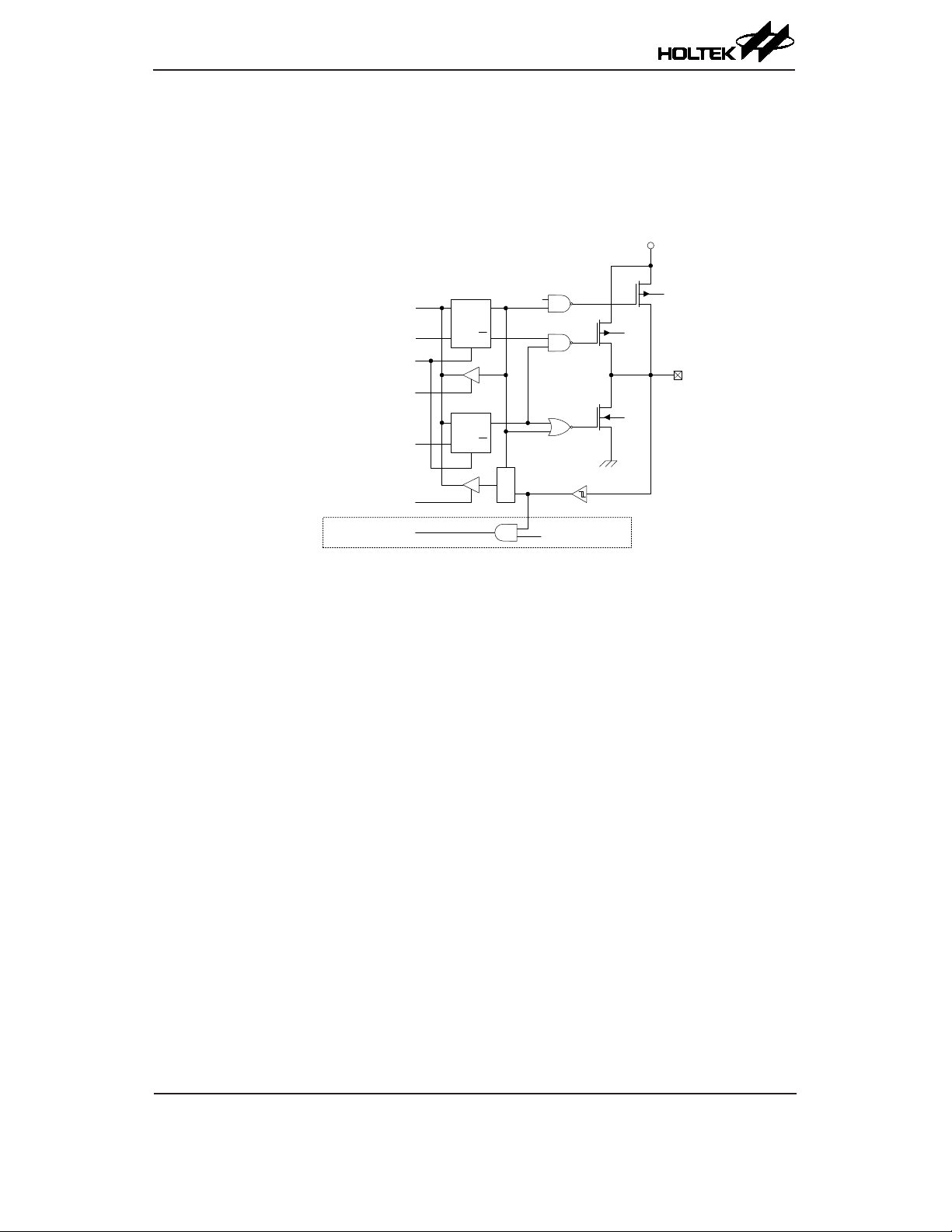
HT45F4050
A/D NFC Flash MCU
I/O Pin Structures
The accompanying diagram illustrates the internal structure of the I/O logic function. As the exact
logical construction of the I/O pin will differ from this diagram, it is supplied as a guide only to
assist with the functional understanding of the logc function I/O pins. The wide range of pin-shared
structures does not permit all types to be shown.
Data Bus
Control Bit
D
Q
Pull-high
Register
Select
VDD
Weak
Pull-up
Write Control Register
Chip Reset
Read Control Register
Write Data Register
Read Data Register
System Wake-up
Programming Considerations
Within the user program, one of the rst things to consider is port initialisation. After a reset, all of
the I/O data and port control registers will be set high. This means that all I/O pins will default to
an input state, the level of which depends on the other connected circuitry and whether pull-high
selections have been chosen. If the port control registers, PAC~PFC, are then programmed to setup
some pins as outputs, these output pins will have an initial high output value unless the associated
port data registers, PA~PF, are first programmed. Selecting which pins are inputs and which are
outputs can be achieved byte-wide by loading the correct values into the appropriate port control
register or by programming individual bits in the port control register using the "SET [m].i" and
"CLR [m].i" instructions. Note that when using these bit control instructions, a read-modify-write
operation takes place. The microcontroller must rst read in the data on the entire port, modify it to
the required new bit values and then rewrite this data back to the output ports.
Port A has the additional capability of providing wake-up functions. When the device is in the
SLEEP or IDLE Mode, various methods are available to wake the device up. One of these is a high
to low transition of any of the Port A pins. Single or multiple pins on Port A can be setup to have this
function.
CK
Q
S
Data Bit
Q
D
Q
CK
S
M
U
X
wake-up Select
Logic Function Input/Output Structure
I/O pin
PA only
Page 78
Timer Modules – TM
One of the most fundamental functions in any microcontroller devices is the ability to control and
measure time. To implement time related functions the device includes several Timer Modules,
generally abbreviated to the name TM. The TMs are multi-purpose timing units and serve to provide
operations such as Timer/Counter, Input Capture, Compare Match Output and Single Pulse Output
as well as being the functional unit for the generation of PWM signals. Each of the TMs has two
interrupts. The addition of input and output pins for each TM ensures that users are provided with
timing units with a wide and exible range of features.
The common features of the different TM types are described here with more detailed information
provided in the individual Compact, Standard and Periodic TM sections.
Introduction
The device contains three TMs and each individual TM can be categorised as a certain type, namely
Compact Type TM, Standard Type TM or Periodic Type TM. Although similar in nature, the
different TM types vary in their feature complexity. The common features to all of the Compact,
Standard and Periodic TMs will be described in this section and the detailed operation regarding
each of the TM types will be described in separate sections. The main features and differences
between the three types of TMs are summarised in the accompanying table.
TM Function CTM STM PTM
Timer/Counter √ √ √
Input Capture — √ √
Compare Match Output √ √ √
PWM Channels 1 1 1
Single Pulse Output — 1 1
PWM Alignment Edge Edge Edge
PWM Adjustment Period & Duty Duty or Period Duty or Period Duty or Period
HT45F4050
A/D NFC Flash MCU
TM Function Summary
TM Operation
The different types of TM offer a diverse range of functions, from simple timing operations to PWM
signal generation. The key to understanding how the TM operates is to see it in terms of a free
running count-up counter whose value is then compared with the value of pre-programmed internal
comparators. When the free running count-up counter has the same value as the pre-programmed
comparator, known as a compare match situation, a TM interrupt signal will be generated which
can clear the counter and perhaps also change the condition of the TM output pin. The internal TM
counter is driven by a user selectable clock source, which can be an internal clock or an external pin.
TM Clock Source
The clock source which drives the main counter in each TM can originate from various sources.
The selection of the required clock source is implemented using the xTCK2~xTCK0 bits in the
xTM control registers, where "x" stands for C, S or P type TM. The clock source can be a ratio of
the system clock, f
The xTCK pin clock source is used to allow an external signal to drive the TM as an external clock
source for event counting.
TM Interrupts
The Compact Type, Standard Type and Periodic Type TMs each have two internal interrupts, one for
each of the internal comparator A or comparator P, which generate a TM interrupt when a compare
match condition occurs. When a TM interrupt is generated it can be used to clear the counter and
also to change the state of the TM output pin.
, or the internal high clock, fH, the f
SYS
clock source or the external xTCK pin.
SUB
Rev. 1.00 78 September 11, 2018 Rev. 1.00 79 September 11, 2018
Page 79
HT45F4050
A/D NFC Flash MCU
TM External Pins
Each of the TMs, irrespective of what type, has one or two TM input pins, with the label xTCK
and xTPI respectively. The xTM input pin, xTCK, is essentially a clock source for the xTM and is
selected using the xTCK2~xTCK0 bits in the xTMC0 register. This external TM input pin allows
an external clock source to drive the internal TM. The xTCK input pin can be chosen to have either
a rising or falling active edge. The STCK and PTCK pins are also used as the external trigger input
pin in single pulse output mode for the STM and PTM respectively.
The other xTM input pin, STPI or PTPI, is the capture input whose active edge can be a rising edge,
a falling edge or both rising and falling edges and the active edge transition type is selected using
the STIO1~STIO0 or PTIO1~PTIO0 bits in the STMC1 or PTMC1 register respectively. There is
another capture input, PTCK, for PTM capture input mode, which can be used as the external trigger
input source except the PTPI pin.
The TMs each have two output pins, xTP and xTPB. The xTPB is the inverted signal of the xTP
output. When the TM is in the Compare Match Output Mode, these pins can be controlled by
the TM to switch to a high or low level or to toggle when a compare match situation occurs. The
external xTP or xTPB output pin is also the pin where the TM generates the PWM output waveform.
As the TM input and output pins are pin-shared with other functions, the TM output function must
first be setup using relevant pin-shared function selection register. The details of the pin-shared
function selection are described in the pin-shared function section.
CTM STM PTM
Input Output Input Output Input Output
CTCK CTP, CTPB STCK, STPI STP, STPB PTCK, PTPI PTP, PTPB
TM External Pins
CTCK
CTM
CCR output
CTM Function Pin Block Diagram
CCR capture input
CTP
CTPB
STCK
STPI
STM
CCR output
STM Function Pin Block Diagram
STP
STPB
Page 80

HT45F4050
A/D NFC Flash MCU
Programming Considerations
The TM Counter Registers and the Capture/Compare CCRA and CCRP registers, all have a low and
high byte structure. The high bytes can be directly accessed, but as the low bytes can only be accessed
via an internal 8-bit buffer, reading or writing to these register pairs must be carried out in a specic
way. The important point to note is that data transfer to and from the 8-bit buffer and its related low
byte only takes place when a write or read operation to its corresponding high byte is executed.
As the CCRA and CCRP registers are implemented in the way shown in the following diagram and
accessing these register pairs is carried out in a specic way as described above, it is recommended
to use the "MOV" instruction to access the CCRA and CCRP low byte registers, named xTMAL and
PTMRPL, using the following access procedures. Accessing the CCRA or CCRP low byte registers
without following these access procedures will result in unpredictable values.
CCR capture input
PTCK
PTPI
PTM
CCR output
PTM Function Pin Block Diagram
xTM Counter Register (Read only)
xTMDHxTMDL
8-bit Buffer
PTP
PTPB
xTMAL
xTM CCRA Register (Read/Write)
PTM CCRP Register (Read/Write)
xTMAH
PTMRPHPTMRPL
Data Bus
The following steps show the read and write procedures:
• Writing Data to CCRA or CCRP
♦
Step 1. Write data to Low Byte xTMAL or PTMRPL
– note that here data is only written to the 8-bit buffer.
♦
Step 2. Write data to High Byte xTMAH or PTMRPH
– here data is written directly to the high byte registers and simultaneously data is latched
from the 8-bit buffer to the Low Byte registers.
• Reading Data from the Counter Registers and CCRA or CCRP
♦
Step 1. Read data from the High Byte xTMDH, xTMAH or PTMRPH
– here data is read directly from the High Byte registers and simultaneously data is latched
from the Low Byte register into the 8-bit buffer.
♦
Step 2. Read data from the Low Byte xTMDL, xTMAL or PTMRPL
– this step reads data from the 8-bit buffer.
Rev. 1.00 80 September 11, 2018 Rev. 1.00 81 September 11, 2018
Page 81

HT45F4050
A/D NFC Flash MCU
Compact Type TM – CTM
Although the simplest form of the three TM types, the Compact TM type still contains three
operating modes, which are Compare Match Output, Timer/Event Counter and PWM Output modes.
The Compact TM can also be controlled with an external input pin and can drive two external output
pins.
CTM Core CTM Input Pin CTM Output Pin
16-bit CTM CTCK CTP, CTPB
CCRP
000
f
/4
SYS
001
f
SYS
010
fH/16
011
CTCK
Pin
Control
PxSn IFS0
fH/64
f
SUB
f
SUB
CTCK2~CTCK0
100
101
110
111
CTON
CTPAU
16-bit Count-up Counter
Compact Type TM Operation
At its core is a 16-bit count-up counter which is driven by a user selectable internal or external clock
source. There are also two internal comparators with the names, Comparator A and Comparator
P. These comparators will compare the value in the counter with CCRP and CCRA registers. The
CCRP is 8-bit wide whose value is compared with the highest eight bits in the counter while the
CCRA is 16-bit wide and therefore compares with all counter bits.
The only way of changing the value of the 16-bit counter using the application program, is to
clear the counter by changing the CTON bit from low to high. The counter will also be cleared
automatically by a counter overow or a compare match with one of its associated comparators.
When these conditions occur, a CTM interrupt signal will also usually be generated. The Compact
Type TM can operate in a number of different operational modes, can be driven by different clock
sources including an input pin and can also control two output pins. All operating setup conditions
are selected using relevant internal registers.
b8~b15
Comparator P Match
Counter Clear
CTCCLR
Comparator A Match
0
1
8-bit Comparator P
b0~b15
16-bit Comparator A
CCRA
Compact Type TM Block Diagram
CTMPF Interrupt
CTOC
Output
Control
CTM1, CTM0
CTIO1, CTIO0
CTMAF Interrupt
Polarity
Control
CTPOL PxSn
Pin
Control
CTP
CTPB
Compact Type TM Register Description
Overall operation of the Compact TM is controlled using a series of registers. A read only register
pair exists to store the internal counter 16-bit value, while a read/write register pair exists to store
the internal 16-bit CCRA value. The CTMRP register is used to store the 8-bit CCRP value. The
remaining two registers are control registers which setup the different operating and control modes.
Register
Name
CTMC0 CTPAU CTCK2 CTCK1 CTCK0 CTON — — —
CTMC1 CTM1 CTM0 CTIO1 CTIO0 CTOC CTPOL CTDPX CTCCLR
CTMDL D7 D6 D5 D4 D3 D2 D1 D0
CTMDH D15 D14 D13 D12 D 11 D10 D9 D8
CTMAL D7 D6 D5 D4 D3 D2 D1 D0
CTMAH D15 D14 D13 D12 D 11 D10 D9 D8
CTMRP CTRP7 CTRP6 CTRP5 CTRP4 CTRP3 CTRP2 CTRP1 CTRP0
7 6 5 4 3 2 1 0
16-bit Compact TM Registers List
Bit
Page 82

HT45F4050
A/D NFC Flash MCU
• CTMC0 Register
Bit 7 6 5 4 3 2 1 0
Name CTPAU CTCK2 CTCK1 CTCK0 CTON — — —
R/W R/W R/W R/W R/W R/W — — —
POR 0 0 0 0 0 — — —
Bit 7 CTPAU: CTM Counter Pause control
0: Run
1: Pause
The counter can be paused by setting this bit high. Clearing the bit to zero restores
normal counter operation. When in a Pause condition the CTM will remain powered
up and continue to consume power. The counter will retain its residual value when
this bit changes from low to high and resume counting from this value when the bit
changes to a low value again.
Bit 6~4 CTCK2~CTCK0: Select CTM Counter clock
000: f
001: f
010: fH/16
011: fH/64
100: f
101: f
110: CTCK rising edge clock
111: CTCK falling edge clock
These three bits are used to select the clock source for the CTM. The external pin
clock source can be chosen to be active on the rising or falling edge. The clock source
f
SYS
can be found in the oscillator section.
Bit 3 CTON: CTM Counter On/Off control
0: Off
1: On
This bit controls the overall on/off function of the CTM. Setting the bit high enables
the counter to run while clearing the bit disables the CTM. Clearing this bit to zero
will stop the counter from counting and turn off the CTM which will reduce its power
consumption. When the bit changes state from low to high the internal counter value
will be reset to zero, however when the bit changes from high to low, the internal
counter will retain its residual value until the bit returns high again. If the CTM is in
the Compare Match Output Mode or the PWM Output Mode then the CTM output pin
will be reset to its initial condition, as specied by the CTOC bit, when the CTON bit
changes from low to high.
Bit 2~0 Unimplemented, read as "0"
/4
SYS
SYS
SUB
SUB
is the system clock, while fH and f
are other internal clocks, the details of which
SUB
• CTMC1 Register
Bit 7 6 5 4 3 2 1 0
Name CTM1 CTM0 CTIO1 CTIO0 CTOC CTPOL CTDPX CTCCLR
R/W R/W R/W R/W R/W R/W R/W R/W R/W
POR 0 0 0 0 0 0 0 0
Bit 7~6 CTM1~CTM0: Select CTM Operating Mode
00: Compare Match Output Mode
01: Undened
10: PWM Output Mode
11: Timer/Counter Mode
These bits setup the required operating mode for the CTM. To ensure reliable
operation the CTM should be switched off before any changes are made to the CTM1
and CTM0 bits. In the Timer/Counter Mode, the CTM output pin state is undened.
Rev. 1.00 82 September 11, 2018 Rev. 1.00 83 September 11, 2018
Page 83

HT45F4050
A/D NFC Flash MCU
Bit 5~4 CTIO1~CTIO0: Select CTM function
Compare Match Output Mode
PWM Output Mode
Timer/Counter Mode
These two bits are used to determine how the CTM output pin changes state when a
certain condition is reached. The function that these bits select depends upon in which
mode the CTM is running.
In the Compare Match Output Mode, the CTIO1 and CTIO0 bits determine how the
CTM output pin changes state when a compare match occurs from the Comparator A.
The CTM output pin can be setup to switch high, switch low or to toggle its present
state when a compare match occurs from the Comparator A. When the bits are both
zero, then no change will take place on the output. The initial value of the CTM output
pin should be setup using the CTOC bit in the CTMC1 register. Note that the output
level requested by the CTIO1 and CTIO0 bits must be different from the initial value
setup using the CTOC bit otherwise no change will occur on the CTM output pin when
a compare match occurs. After the CTM output pin changes state, it can be reset to its
initial level by changing the level of the CTON bit from low to high.
In the PWM Output Mode, the CTIO1 and CTIO0 bits determine how the CTM
output pin changes state when a certain compare match condition occurs. The PWM
output function is modied by changing these two bits. It is necessary to only change
the values of the CTIO1 and CTIO0 bits only after the CTM has been switched off.
Unpredictable PWM outputs will occur if the CTIO1 and CTIO0 bits are changed
when the CTM is running.
Bit 3 CTOC: CTP Output control
Compare Match Output Mode
PWM Output Mode
This is the output control bit for the CTM output pin. Its operation depends upon
whether CTM is being used in the Compare Match Output Mode or in the PWM
Output Mode. It has no effect if the CTM is in the Timer/Counter Mode. In the
Compare Match Output Mode it determines the logic level of the CTM output pin
before a compare match occurs. In the PWM Output Mode it determines if the PWM
signal is active high or active low.
Bit 2 CTPOL: CTP Output polarity control
This bit controls the polarity of the CTP output pin. When the bit is set high the CTM
output pin will be inverted and not inverted when the bit is zero. It has no effect if the
TM is in the Timer/Counter Mode.
Bit 1 CTDPX: CTM PWM duty/period control
This bit determines which of the CCRA and CCRP registers are used for period and
duty control of the PWM waveform.
00: No change
01: Output low
10: Output high
11: Toggle output
00: PWM output inactive state
01: PWM output active state
10: PWM output
11: Undened
Unused
0: Initial low
1: Initial high
0: Active low
1: Active high
0: Non-invert
1: Invert
0: CCRP – period; CCRA – duty
1: CCRP – duty; CCRA – period
Page 84

HT45F4050
A/D NFC Flash MCU
Bit 0 CTCCLR: CTM Counter Clear condition selection
0: CTM Comparator P match
1: CTM Comparator A match
This bit is used to select the method which clears the counter. Remember that the
Compact TM contains two comparators, Comparator A and Comparator P, either of
which can be selected to clear the internal counter. With the CTCCLR bit set high,
the counter will be cleared when a compare match occurs from the Comparator A.
When the bit is low, the counter will be cleared when a compare match occurs from
the Comparator P or with a counter overow. A counter overow clearing method can
only be implemented if the CCRP bits are all cleared to zero. The CTCCLR bit is not
used in the PWM Output Mode.
• CTMDL Register
Bit 7 6 5 4 3 2 1 0
Name D7 D6 D5 D4 D3 D2 D1 D0
R/W R R R R R R R R
POR 0 0 0 0 0 0 0 0
Bit 7~0 CTM Counter Low Byte Register bit 7 ~ bit 0
CTM 16-bit Counter bit 7 ~ bit 0
• CTMDH Register
Bit 7 6 5 4 3 2 1 0
Name D15 D14 D13 D12 D11 D10 D9 D8
R/W R R R R R R R R
POR 0 0 0 0 0 0 0 0
Bit 7~0 CTM Counter High Byte Register bit 7 ~ bit 0
CTM 16-bit Counter bit 15 ~ bit 8
• CTMAL Register
Bit 7 6 5 4 3 2 1 0
Name D7 D6 D5 D4 D3 D2 D1 D0
R/W R/W R/W R/W R/W R/W R/W R/W R/W
POR 0 0 0 0 0 0 0 0
Bit 7~0 CTM CCRA Low Byte Register bit 7 ~ bit 0
CTM 16-bit CCRA bit 7 ~ bit 0
• CTMAH Register
Bit 7 6 5 4 3 2 1 0
Name D15 D14 D13 D12 D11 D10 D9 D8
R/W R/W R/W R/W R/W R/W R/W R/W R/W
POR 0 0 0 0 0 0 0 0
Bit 7~0 CTM CCRA High Byte Register bit 7 ~ bit 0
CTM 16-bit CCRA bit 15 ~ bit 8
Rev. 1.00 84 September 11, 2018 Rev. 1.00 85 September 11, 2018
Page 85

HT45F4050
A/D NFC Flash MCU
• CTMRP Register
Bit 7 6 5 4 3 2 1 0
Name CTRP7 CTRP6 CTRP5 CTRP4 CTRP3 CTRP2 CTRP1 CTRP0
R/W R/W R/W R/W R/W R/W R/W R/W R/W
POR 0 0 0 0 0 0 0 0
Bit 7~0
CTRP7~CTRP0: CTM CCRP 8-bit register, compared with the CTM Counter bit 15 ~ bit 8
Comparator P Match Period=
0: 65536 CTM clocks
1~255: 256 × (1~255) CTM clocks
These eight bits are used to setup the value on the internal CCRP 8-bit register, which
are then compared with the internal counter's highest eight bits. The result of this
comparison can be selected to clear the internal counter if the CTCCLR bit is set to
zero. Setting the CTCCLR bit to zero ensures that a compare match with the CCRP
values will reset the internal counter. As the CCRP bits are only compared with the
highest eight counter bits, the compare values exist in 256 clock cycle multiples.
Clearing all eight bits to zero is in effect allowing the counter to overflow at its
maximum value.
Compact Type TM Operating Modes
The Compact Type TM can operate in one of three operating modes, Compare Match Output Mode,
PWM Output Mode or Timer/Counter Mode. The operating mode is selected using the CTM1 and
CTM0 bits in the CTMC1 register.
Compare Match Output Mode
To select this mode, bits CTM1 and CTM0 in the CTMC1 register, should be set to "00"
respectively. In this mode once the counter is enabled and running it can be cleared by three
methods. These are a counter overow, a compare match from Comparator A and a compare match
from Comparator P. When the CTCCLR bit is low, there are two ways in which the counter can be
cleared. One is when a compare match occurs from Comparator P, the other is when the CCRP bits
are all zero which allows the counter to overow. Here both CTMAF and CTMPF interrupt request
ags for the Comparator A and Comparator P respectively, will both be generated.
If the CTCCLR bit in the CTMC1 register is high then the counter will be cleared when a compare
match occurs from Comparator A. However, here only the CTMAF interrupt request ag will be
generated even if the value of the CCRP bits is less than that of the CCRA registers. Therefore when
CTCCLR is high no CTMPF interrupt request ag will be generated. If the CCRA bits are all zero,
the counter will overow when its reaches its maximum 16-bit, FFFF Hex, value, however here the
CTMAF interrupt request ag will not be generated.
As the name of the mode suggests, after a comparison is made, the CTM output pin will change
state. The CTM output pin condition however only changes state when a CTMAF interrupt request
ag is generated after a compare match occurs from Comparator A. The CTMPF interrupt request
ag, generated from a compare match occurs from Comparator P, will have no effect on the CTM
output pin. The way in which the CTM output pin changes state are determined by the condition of
the CTIO1 and CTIO0 bits in the CTMC1 register. The CTM output pin can be selected using the
CTIO1 and CTIO0 bits to go high, to go low or to toggle from its present condition when a compare
match occurs from Comparator A. The initial condition of the CTM output pin, which is setup after
the CTON bit changes from low to high, is setup using the CTOC bit. Note that if the CTIO1 and
CTIO0 bits are zero then no pin change will take place.
Page 86

HT45F4050
A/D NFC Flash MCU
CCRP=0
Counter overflow
CCRP > 0
CCRP > 0
Counter cleared by CCRP value
Resume
Pause
Counter Value
0xFFFF
CCRP
CCRA
CTON
CTPAU
CTPOL
CCRP Int. flag
CTMPF
CCRA Int. flag
CTMAF
CTM O/P Pin
Output not affected by
Output pin set to
initial Level Low if
CTOC=0
Output Toggle
with CTMAF flag
Here CTIO [1:0] = 11
Toggle Output select
Note CTIO [1:0] = 10
Active High Output select
CTMAF flag. Remains High
until reset by CTON bit
Compare Match Output Mode – CTCCLR=0
Note: 1. With CTCCLR=0, a Comparator P match will clear the counter
2. The CTM output pin is controlled only by the CTMAF ag
3. The output pin is reset to its initial state by a CTON bit rising edge
CTCCLR = 0; CTM [1:0] = 00
Counter
Restart
Stop
Output Inverts
Output Pin
Output controlled by other
pin-shared function
Reset to Initial value
when CTPOL is high
Time
Rev. 1.00 86 September 11, 2018 Rev. 1.00 87 September 11, 2018
Page 87

HT45F4050
A/D NFC Flash MCU
Counter Value
CCRA > 0 Counter cleared by CCRA value
0xFFFF
CCRA
Resume
Pause
CCRP
CTON
CTPAU
CTPOL
CCRA Int. flag
CTMAF
CCRP Int. flag
CTMPF
CTMPF not
generated
CTM O/P Pin
Output not affected by
Output pin set to
initial Level Low if
CTOC=0
Output Toggle
with CTMAF flag
Here CTIO [1:0] = 11
Toggle Output select
Note CTIO [1:0] = 10
Active High Output select
CTMAF flag. Remains High
until reset by CTON bit
Compare Match Output Mode – CTCCLR=1
Note: 1. With CTCCLR=1, a Comparator A match will clear the counter
2. The CTM output pin is controlled only by the CTMAF ag
3. The output pin is reset to its initial state by a CTON bit rising edge
4. The CTMPF ag is not generated when CTCCLR=1
CTCCLR = 1; CTM [1:0] = 00
CCRA = 0
Counter overflow
CCRA=0
Stop
Counter Restart
No CTMAF flag
generated on
CCRA overflow
Output Inverts
Output Pin
Reset to Initial value
Output controlled by other
pin-shared function
when CTPOL is high
Time
Output does
not change
Page 88

HT45F4050
A/D NFC Flash MCU
Timer/Counter Mode
To select this mode, bits CTM1 and CTM0 in the CTMC1 register should be set to 11 respectively.
The Timer/Counter Mode operates in an identical way to the Compare Match Output Mode
generating the same interrupt flags. The exception is that in the Timer/Counter Mode the CTM
output pin is not used. Therefore the above description and Timing Diagrams for the Compare
Match Output Mode can be used to understand its function. As the CTM output pin is not used in
this mode, the pin can be used as a normal I/O pin or other pin-shared functions.
PWM Output Mode
To select this mode, bits CTM1 and CTM0 in the CTMC1 register should be set to 10 respectively.
The PWM function within the CTM is useful for applications which require functions such as motor
control, heating control, illumination control etc. By providing a signal of xed frequency but of
varying duty cycle on the CTM output pin, a square wave AC waveform can be generated with
varying equivalent DC RMS values.
As both the period and duty cycle of the PWM waveform can be controlled, the choice of generated
waveform is extremely exible. In the PWM Output Mode, the CTCCLR bit has no effect on the
PWM operation. Both of the CCRA and CCRP registers are used to generate the PWM waveform,
one register is used to clear the internal counter and thus control the PWM waveform frequency,
while the other one is used to control the duty cycle. Which register is used to control either
frequency or duty cycle is determined using the CTDPX bit in the CTMC1 register. The PWM
waveform frequency and duty cycle can therefore be controlled by the values in the CCRA and
CCRP registers.
An interrupt ag, one for each of the CCRA and CCRP, will be generated when a compare match
occurs from either Comparator A or Comparator P. The CTOC bit in the CTMC1 register is used to
select the required polarity of the PWM waveform while the two CTIO1 and CTIO0 bits are used to
enable the PWM output or to force the TM output pin to a xed high or low level. The CTPOL bit is
used to reverse the polarity of the PWM output waveform.
• 16-bit CTM, PWM Output Mode, Edge-aligned Mode, CTDPX=0
CCRP 1~255 0
Period CCRP×256 65536
Duty CCRA
If f
=16MHz, CTM clock source select f
SYS
The CTM PWM output frequency=(f
SYS
/4, CCRP=2 and CCRA=128,
SYS
/4)/(2×256)=f
/2048=7.8125kHz, duty=128/(2×256)=25%.
SYS
If the Duty value dened by the CCRA register is equal to or greater than the Period value, then the
PWM output duty is 100%.
• 16-bit CTM, PWM Output Mode, Edge-aligned Mode, CTDPX=1
CCRP 1~255 0
Period CCRA
Duty CCRP×256 65536
The PWM output period is determined by the CCRA register value together with the CTM clock
while the PWM duty cycle is dened by the CCRP register value except when the CCRP value is
equal to 0.
Rev. 1.00 88 September 11, 2018 Rev. 1.00 89 September 11, 2018
Page 89

HT45F4050
A/D NFC Flash MCU
Counter Value
CCRP
CCRA
CTON
CTPAU
CTPOL
CCRA Int.
flag CTMAF
CCRP Int.
flag CTMPF
CTM O/P Pin
(CTOC=1)
CTM O/P Pin
(CTOC=0)
Counter cleared by
CCRP
Pause
CTDPX = 0; CTM [1:0] = 10
Resume
Counter Stop if
CTON bit low
Counter Reset when
CTON returns high
Time
PWM Duty Cycle
set by CCRA
PWM Period set by CCRP
PWM Output Mode – CTDPX=0
Note: 1. Here CTDPX=0 – Counter cleared by CCRP
2. A counter clear sets the PWM Period
3. The internal PWM function continues even when CTIO [1:0]=00 or 01
4. The CTCCLR bit has no inuence on PWM operation
PWM resumes
Output controlled by other
pin-shared function
operation
Output Inverts
when CTPOL = 1
Page 90
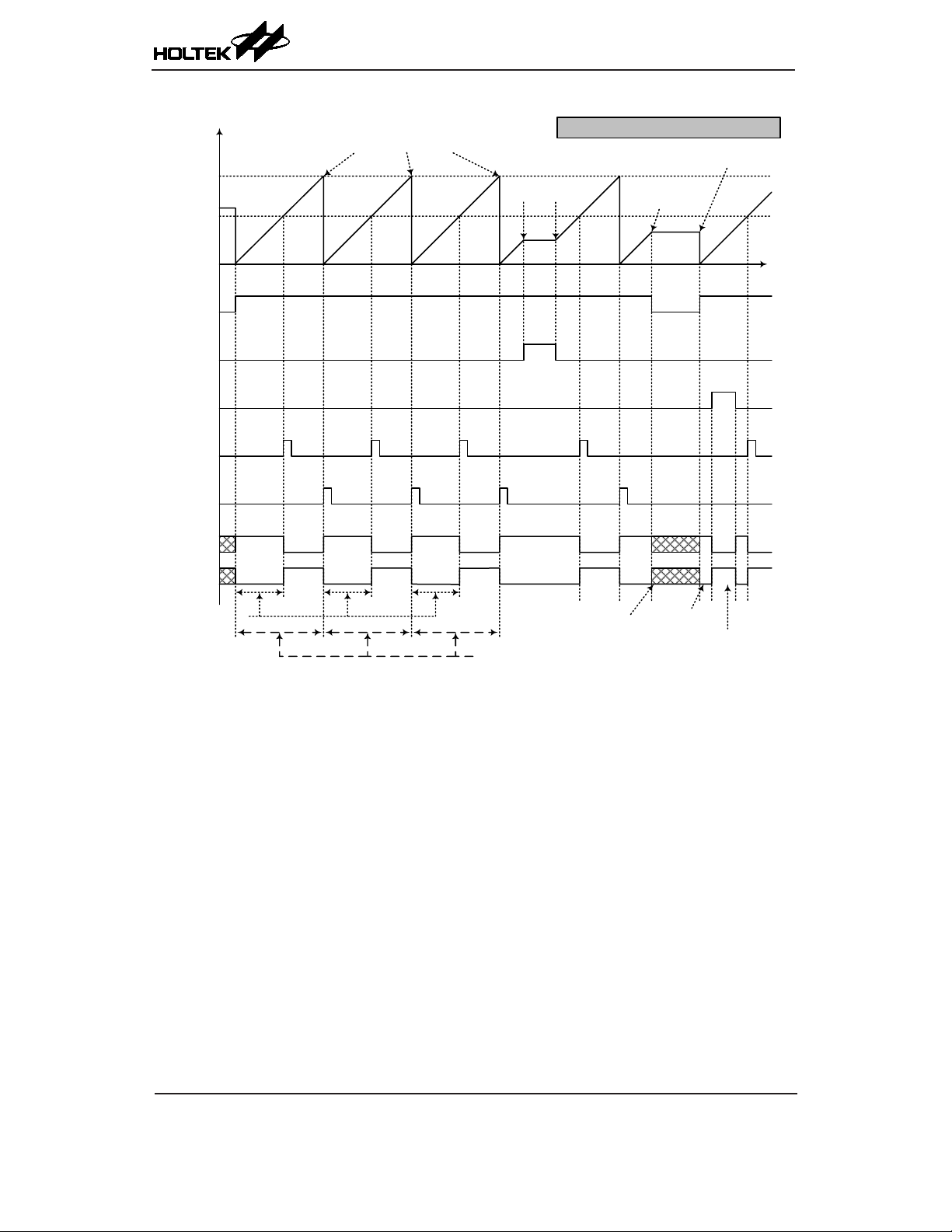
HT45F4050
A/D NFC Flash MCU
Counter Value
CCRA
CCRP
CTON
CTPAU
CTPOL
CCRP Int.
flag CTMPF
CCRA Int.
flag CTMAF
CTM O/P Pin
(CTOC=1)
CTM O/P Pin
(CTOC=0)
Counter cleared by
CCRA
Pause
CTDPX = 1; CTM [1:0] = 10
Resume
Counter Stop if
CTON bit low
Counter Reset when
CTON returns high
Time
PWM Duty Cycle
set by CCRP
PWM Period set by CCRA
PWM Output Mode – CTDPX=1
Note: 1. Here CTDPX=1 – Counter cleared by CCRA
2. A counter clear sets the PWM Period
3. The internal PWM function continues even when CTIO [1:0]=00 or 01
4. The CTCCLR bit has no inuence on PWM operation
Output controlled by
other pin-shared function
PWM resumes
operation
Output Inverts
when CTPOL = 1
Rev. 1.00 90 September 11, 2018 Rev. 1.00 91 September 11, 2018
Page 91

HT45F4050
A/D NFC Flash MCU
Standard Type TM – STM
The Standard Type TM contains ve operating modes, which are Compare Match Output, Timer/
Event Counter, Capture Input, Single Pulse Output and PWM Output modes. The Standard TM can
also be controlled with two external input pins and can drive two external output pins.
STM Core STM Input Pin STM Output Pin
16-bit STM STCK, STPI STP, STPB
CCRP
8-bit Comparator P
16-bit Count-up Counter
STON
STPAU
16-bit Comparator A
STCK
Pin
Control
PxSn IFS0
f
/4
SYS
f
SYS
fH/16
fH/64
f
SUB
f
SUB
STCK2~STCK0
000
001
010
011
100
101
110
111
Standard Type TM Block Diagram
Standard Type TM Operation
The size of Standard TM is 16-bit wide and its core is a 16-bit count-up counter which is driven by
a user selectable internal or external clock source. There are also two internal comparators with the
names, Comparator A and Comparator P. These comparators will compare the value in the counter with
CCRP and CCRA registers. The CCRP comparator is 8-bit wide whose value is compared the with
highest 8 bits in the counter while the CCRA is the sixteen bits and therefore compares all counter bits.
The only way of changing the value of the 16-bit counter using the application program, is to
clear the counter by changing the STON bit from low to high. The counter will also be cleared
automatically by a counter overow or a compare match with one of its associated comparators.
When these conditions occur, a STM interrupt signal will also usually be generated. The Standard
Type TM can operate in a number of different operational modes, can be driven by different clock
sources including an input pin and can also control two output pins. All operating setup conditions
are selected using relevant internal registers.
CCRA
b8~b15
b0~b15
Comparator P Match
Counter Clear
STCCLR
Comparator A Match
STIO1, STIO0
Edge
Detector
STMPF Interrupt
STOC
0
1
Output
Control
STM1, STM0
STIO1, STIO0
PxSn IFS0
Control
Polarity
Control
STMAF Interrupt
Pin
STPOL
STPI
Pin
Control
PxSn
STP
STPB
Standard Type TM Register Description
Overall operation of the Standard TM is controlled using a series of registers. A read only register
pair exists to store the internal counter 16-bit value, while a read/write register pair exists to store
the internal 16-bit CCRA value. The STMRP register is used to store the 8-bit CCRP value. The
remaining two registers are control registers which setup the different operating and control modes.
Register
Name
STMC0 STPAU STCK2 STCK1 STCK0 STON — — —
STMC1 STM1 STM0 STIO1 STIO0 STOC STPOL STDPX STCCLR
STMDL D7 D6 D5 D4 D3 D2 D1 D0
STMDH D15 D14 D13 D12 D11 D10 D9 D8
STMAL D7 D6 D5 D4 D3 D2 D1 D0
STMAH D15 D14 D13 D12 D 11 D10 D9 D8
STMRP STRP7 STRP6 STRP5 STRP4 STRP3 STRP2 STRP1 STRP0
7 6 5 4 3 2 1 0
16-bit Standard TM Registers List
Bit
Page 92

HT45F4050
A/D NFC Flash MCU
• STMC0 Register
Bit 7 6 5 4 3 2 1 0
Name STPAU STCK2 STCK1 STCK0 STON — — —
R/W R/W R/W R/W R/W R/W — — —
POR 0 0 0 0 0 — — —
Bit 7 STPAU: STM Counter Pause control
0: Run
1: Pause
The counter can be paused by setting this bit high. Clearing the bit to zero restores
normal counter operation. When in a Pause condition the STM will remain powered
up and continue to consume power. The counter will retain its residual value when
this bit changes from low to high and resume counting from this value when the bit
changes to a low value again.
Bit 6~4 STCK2~STCK0: Select STM Counter clock
000: f
001: f
010: fH/16
011: fH/64
100: f
101: f
110: STCK rising edge clock
111: STCK falling edge clock
These three bits are used to select the clock source for the STM. The external pin clock
source can be chosen to be active on the rising or falling edge. The clock source f
the system clock, while fH and f
be found in the oscillator section.
Bit 3 STON: STM Counter On/Off control
0: Off
1: On
This bit controls the overall on/off function of the STM. Setting the bit high enables
the counter to run while clearing the bit disables the STM. Clearing this bit to zero
will stop the counter from counting and turn off the STM which will reduce its power
consumption. When the bit changes state from low to high the internal counter value
will be reset to zero, however when the bit changes from high to low, the internal
counter will retain its residual value until the bit returns high again. If the STM is in
the Compare Match Output Mode or PWM output Mode or Single Pulse Output Mode,
then the STM output pin will be reset to its initial condition, as specied by the STOC
bit, when the STON bit changes from low to high.
Bit 2~0 Unimplemented, read as "0"
SYS
SYS
SUB
SUB
/4
are other internal clocks, the details of which can
SUB
SYS
is
• STMC1 Register
Bit 7 6 5 4 3 2 1 0
Name STM1 STM0 STIO1 STIO0 STOC STPOL STDPX STCCLR
R/W R/W R/W R/W R/W R/W R/W R/W R/W
POR 0 0 0 0 0 0 0 0
Bit 7~6 STM1~STM0: Select STM Operating Mode
00: Compare Match Output Mode
01: Capture Input Mode
10: PWM Output Mode or Single Pulse Output Mode
11: Timer/Counter Mode
These bits setup the required operating mode for the STM. To ensure reliable operation
the STM should be switched off before any changes are made to the STM1 and STM0
bits. In the Timer/Counter Mode, the STM output pin state is undened.
Rev. 1.00 92 September 11, 2018 Rev. 1.00 93 September 11, 2018
Page 93

HT45F4050
A/D NFC Flash MCU
Bit 5~4 STIO1~STIO0: Select STM external pin function
Compare Match Output Mode
PWM Output Mode/Single Pulse Output Mode
Capture Input Mode
Timer/Counter Mode
These two bits are used to determine how the STM output pin changes state when a
certain condition is reached. The function that these bits select depends upon in which
mode the STM is running.
In the Compare Match Output Mode, the STIO1 and STIO0 bits determine how the
STM output pin changes state when a compare match occurs from the Comparator
A. The TM output pin can be setup to switch high, switch low or to toggle its present
state when a compare match occurs from the Comparator A. When the bits are both
zero, then no change will take place on the output. The initial value of the STM output
pin should be setup using the STOC bit in the STMC1 register. Note that the output
level requested by the STIO1 and STIO0 bits must be different from the initial value
setup using the STOC bit otherwise no change will occur on the STM output pin when
a compare match occurs. After the STM output pin changes state, it can be reset to its
initial level by changing the level of the STON bit from low to high.
In the PWM Output Mode, the STIO1 and STIO0 bits determine how the STM
output pin changes state when a certain compare match condition occurs. The PWM
output function is modied by changing these two bits. It is necessary to only change
the values of the STIO1 and STIO0 bits only after the STM has been switched off.
Unpredictable PWM outputs will occur if the STIO1 and STIO0 bits are changed
when the STM is running.
Bit 3 STOC: STM STP Output control
Compare Match Output Mode
PWM Output Mode/Single Pulse Output Mode
This is the output control bit for the STM output pin. Its operation depends upon whether
STM is being used in the Compare Match Output Mode or in the PWM Output Mode/
Single Pulse Output Mode. It has no effect if the STM is in the Timer/Counter Mode. In
the Compare Match Output Mode it determines the logic level of the STM output pin
before a compare match occurs. In the PWM Output Mode it determines if the PWM
signal is active high or active low. In the Single Pulse Output Mode it determines the
logic level of the STM output pin when the STON bit changes from low to high.
Bit 2 STPOL: STM STP Output polarity control
This bit controls the polarity of the STP output pin. When the bit is set high the STM
output pin will be inverted and not inverted when the bit is zero. It has no effect if the
STM is in the Timer/Counter Mode.
00: No change
01: Output low
10: Output high
11: Toggle output
00: PWM output inactive state
01: PWM output active state
10: PWM output
11: Single Pulse Output
00: Input capture at rising edge of STPI
01: Input capture at falling edge of STPI
10: Input capture at rising/falling edge of STPI
11: Input capture disabled
Unused
0: Initial low
1: Initial high
0: Active low
1: Active high
0: Non-invert
1: Invert
Page 94
HT45F4050
A/D NFC Flash MCU
Bit 1 STDPX: STM PWM duty/period control
0: CCRP – period; CCRA – duty
1: CCRP – duty; CCRA – period
This bit determines which of the CCRA and CCRP registers are used for period and
duty control of the PWM waveform.
Bit 0 STCCLR: STM Counter Clear condition selection
0: Comparator P match
1: Comparator A match
This bit is used to select the method which clears the counter. Remember that the
Standard TM contains two comparators, Comparator A and Comparator P, either of
which can be selected to clear the internal counter. With the STCCLR bit set high,
the counter will be cleared when a compare match occurs from the Comparator A.
When the bit is low, the counter will be cleared when a compare match occurs from
the Comparator P or with a counter overow. A counter overow clearing method can
only be implemented if the CCRP bits are all cleared to zero. The STCCLR bit is not
used in the PWM Output Mode, Single Pulse Output Mode or Capture Input Mode.
• STMDL Register
Bit 7 6 5 4 3 2 1 0
Name D7 D6 D5 D4 D3 D2 D1 D0
R/W R R R R R R R R
POR 0 0 0 0 0 0 0 0
Bit 7~0 D7~D0: STM Counter Low Byte Register bit 7 ~ bit 0
STM 16-bit Counter bit 7 ~ bit 0
• STMDH Register
Bit 7 6 5 4 3 2 1 0
Name D15 D14 D13 D12 D11 D10 D9 D8
R/W R R R R R R R R
POR 0 0 0 0 0 0 0 0
Bit 7~0 D15~D8: STM Counter High Byte Register bit 7 ~ bit 0
STM 16-bit Counter bit 15 ~ bit 8
• STMAL Register
Bit 7 6 5 4 3 2 1
Name D7 D6 D5 D4 D3 D2 D1 D0
R/W
POR
R/W R/W R/W R/W R/W R/W R/W R/W
0 0 0 0 0 0 0
Bit 7~0 D7~D0: STM CCRA Low Byte Register bit 7 ~ bit 0
STM 16-bit CCRA bit 7 ~ bit 0
• STMAH Register
Bit 7 6 5 4 3 2 1 0
Name D15 D14 D13 D12 D11 D10 D9 D8
R/W R/W R/W R/W R/W R/W R/W R/W R/W
POR 0 0 0 0 0 0 0 0
0
0
Bit 7~0 D15~D8: STM CCRA High Byte Register bit 7 ~ bit 0
STM 16-bit CCRA bit 15 ~ bit 8
Rev. 1.00 94 September 11, 2018 Rev. 1.00 95 September 11, 2018
Page 95

HT45F4050
A/D NFC Flash MCU
• STMRP Register
Bit 7 6 5 4 3 2 1 0
Name STRP7 STRP6 STRP5 STRP4 STRP3 STRP2 STRP1 STRP0
R/W R/W R/W R/W R/W R/W R/W R/W R/W
POR 0 0 0 0 0 0 0 0
Bit 7~0
STRP7~STRP0: STM CCRP 8-bit register, compared with the STM counter bit 15~bit 8
Comparator P match period=
0: 65536 STM clocks
1~255: (1~255) × 256 STM clocks
These eight bits are used to setup the value on the internal CCRP 8-bit register, which
are then compared with the internal counter's highest eight bits. The result of this
comparison can be selected to clear the internal counter if the STCCLR bit is set to
zero. Setting the STCCLR bit to zero ensures that a compare match with the CCRP
values will reset the internal counter. As the CCRP bits are only compared with the
highest eight counter bits, the compare values exist in 256 clock cycle multiples.
Clearing all eight bits to zero is in effect allowing the counter to overflow at its
maximum value.
Standard Type TM Operation Modes
The Standard Type TM can operate in one of ve operating modes, Compare Match Output Mode,
PWM Output Mode, Single Pulse Output Mode, Capture Input Mode or Timer/Counter Mode. The
operating mode is selected using the STM1 and STM0 bits in the STMC1 register.
Compare Match Output Mode
To select this mode, bits STM1 and STM0 in the STMC1 register, should be set to 00 respectively.
In this mode once the counter is enabled and running it can be cleared by three methods. These are
a counter overow, a compare match from Comparator A and a compare match from Comparator P.
When the STCCLR bit is low, there are two ways in which the counter can be cleared. One is when
a compare match from Comparator P, the other is when the CCRP bits are all zero which allows the
counter to overow. Here both STMAF and STMPF interrupt request ags for Comparator A and
Comparator P respectively, will both be generated.
If the STCCLR bit in the STMC1 register is high then the counter will be cleared when a compare
match occurs from Comparator A. However, here only the STMAF interrupt request ag will be
generated even if the value of the CCRP bits is less than that of the CCRA registers. Therefore when
STCCLR is high no STMPF interrupt request ag will be generated. In the Compare Match Output
Mode, the CCRA can not be set to "0".
If the CCRA bits are all zero, the counter will overow when its reaches its maximum 16-bit, FFFF
Hex, value, however here the STMAF interrupt request ag will not be generated.
As the name of the mode suggests, after a comparison is made, the STM output pin, will change
state. The STM output pin condition however only changes state when a STMAF interrupt request
ag is generated after a compare match occurs from Comparator A. The STMPF interrupt request
ag, generated from a compare match occurs from Comparator P, will have no effect on the STM
output pin. The way in which the STM output pin changes state are determined by the condition of
the STIO1 and STIO0 bits in the STMC1 register. The STM output pin can be selected using the
STIO1 and STIO0 bits to go high, to go low or to toggle from its present condition when a compare
match occurs from Comparator A. The initial condition of the STM output pin, which is setup after
the STON bit changes from low to high, is setup using the STOC bit. Note that if the STIO1 and
STIO0 bits are zero then no pin change will take place.
Page 96

HT45F4050
A/D NFC Flash MCU
CCRP=0
Counter overflow
CCRP > 0
CCRP > 0
Counter cleared by CCRP value
Resume
Pause
Counter Value
0xFFFF
CCRP
CCRA
STON
STPAU
STPOL
CCRP Int. flag
STMPF
CCRA Int. flag
STMAF
STM O/P Pin
Output not affected by
Output pin set
to initial Level
Low if STOC=0
Output Toggle
with STMAF flag
Here STIO [1:0] = 11
Toggle Output select
Note STIO [1:0] = 10
Active High Output select
STMAF flag. Remains High
until reset by STON bit
Compare Match Output Mode – STCCLR=0
Note: 1. With STCCLR=0, a Comparator P match will clear the counter
2. The STM output pin is controlled only by the STMAF ag
3. The output pin is reset to its initial state by a STON bit rising edge
STCCLR = 0; STM [1:0] = 00
Counter
Restart
Stop
Output Inverts
Output Pin
Output controlled by
other pin-shared function
Reset to Initial value
when STPOL is high
Time
Rev. 1.00 96 September 11, 2018 Rev. 1.00 97 September 11, 2018
Page 97

HT45F4050
A/D NFC Flash MCU
Counter Value
CCRA > 0 Counter cleared by CCRA value
0xFFFF
CCRA
Resume
Pause
CCRP
STON
STPAU
STPOL
CCRA Int.
flag STMAF
CCRP Int.
flag STMPF
STMPF not
STM O/P Pin
generated
Output pin set
to initial Level
Low if STOC=0
Output Toggle
with STMAF flag
Here STIO [1:0] = 11
Toggle Output select
Output not affected by
STMAF flag. Remains High
until reset by STON bit
Note STIO [1:0] = 10
Active High Output select
Compare Match Output Mode – STCCLR=1
Note: 1. With STCCLR=1, a Comparator A match will clear the counter
2. The STM output pin is controlled only by the STMAF ag
3. The output pin is reset to its initial state by a STON bit rising edge
4. The STMPF ag is not generated when STCCLR=1
STCCLR = 1; STM [1:0] = 00
CCRA = 0
Counter overflow
CCRA=0
Stop
Counter Restart
Output Inverts
Output Pin
Reset to Initial value
Output controlled by
other pin-shared function
when STPOL is high
Time
No STMAF flag
generated on
CCRA overflow
Output
does not
change
Page 98

HT45F4050
A/D NFC Flash MCU
Timer/Counter Mode
To select this mode, bits STM1 and STM0 in the STMC1 register should be set to 11 respectively.
The Timer/Counter Mode operates in an identical way to the Compare Match Output Mode
generating the same interrupt flags. The exception is that in the Timer/Counter Mode the STM
output pin is not used. Therefore the above description and Timing Diagrams for the Compare
Match Output Mode can be used to understand its function. As the STM output pin is not used in
this mode, the pin can be used as a normal I/O pin or other pin-shared functions.
PWM Output Mode
To select this mode, bits STM1 and STM0 in the STMC1 register should be set to 10 respectively
and also the STIO1 and STIO0 bits should be set to 10 respectively. The PWM function within
the STM is useful for applications which require functions such as motor control, heating control,
illumination control etc. By providing a signal of xed frequency but of varying duty cycle on the
STM output pin, a square wave AC waveform can be generated with varying equivalent DC RMS
values.
As both the period and duty cycle of the PWM waveform can be controlled, the choice of generated
waveform is extremely exible. In the PWM Output Mode, the STCCLR bit has no effect as the
PWM period. Both of the CCRA and CCRP registers are used to generate the PWM waveform, one
register is used to clear the internal counter and thus control the PWM waveform frequency, while
the other one is used to control the duty cycle. Which register is used to control either frequency
or duty cycle is determined using the STDPX bit in the STMC1 register. The PWM waveform
frequency and duty cycle can therefore be controlled by the values in the CCRA and CCRP registers.
An interrupt ag, one for each of the CCRA and CCRP, will be generated when a compare match
occurs from either Comparator A or Comparator P. The STOC bit in the STMC1 register is used to
select the required polarity of the PWM waveform while the two STIO1 and STIO0 bits are used to
enable the PWM output or to force the STM output pin to a xed high or low level. The STPOL bit
is used to reverse the polarity of the PWM output waveform.
• 16-bit STM, PWM Output Mode, Edge-aligned Mode, STDPX=0
CCRP 1~255 0
Period CCRP×256 65536
Duty CCRA
If f
=16MHz, STM clock source is f
SYS
The STM PWM output frequency=(f
/4, CCRP=2 and CCRA=128,
SYS
/4)/(2×256)=f
SYS
/2048=7.8125 kHz, duty=128/(2×256)=25%.
SYS
If the Duty value dened by the CCRA register is equal to or greater than the Period value, then the
PWM output duty is 100%.
• 16-bit STM, PWM Output Mode, Edge-aligned Mode, STDPX=1
CCRP 1~255 0
Period CCRA
Duty CCRP×256 65536
The PWM output period is determined by the CCRA register value together with the TM clock
while the PWM duty cycle is dened by the CCRP register value except when the CCRP value is
equal to 0.
Rev. 1.00 98 September 11, 2018 Rev. 1.00 99 September 11, 2018
Page 99

HT45F4050
A/D NFC Flash MCU
Counter Value
CCRP
CCRA
STON
STPAU
STPOL
CCRA Int.
flag STMAF
CCRP Int.
flag STMPF
STM O/P Pin
(STOC=1)
STM O/P Pin
(STOC=0)
PWM Duty Cycle
set by CCRA
Counter cleared by
CCRP
PWM Period set by CCRP
PWM Output Mode – STDPX=0
Note: 1. Here STDPX=0 – Counter cleared by CCRP
2. A counter clear sets the PWM Period
3. The internal PWM function continues even when STIO [1:0]=00 or 01
4. The STCCLR bit has no inuence on PWM operation
Pause
STDPX = 0; STM [1:0] = 10
Resume
Output controlled by
other pin-shared function
Counter Stop if
STON bit low
Counter Reset when
STON returns high
PWM resumes
operation
Output Inverts
when STPOL = 1
Time
Page 100

HT45F4050
A/D NFC Flash MCU
Counter Value
CCRA
CCRP
STON
STPAU
STPOL
CCRP Int.
flag STMPF
CCRA Int.
flag STMAF
STM O/P Pin
(STOC=1)
STM O/P Pin
(STOC=0)
Counter cleared by
CCRA
Pause
STDPX = 1; STM [1:0] = 10
Resume
Counter Stop if
STON bit low
Counter Reset when
STON returns high
Time
PWM Duty Cycle
set by CCRP
PWM Period set by CCRA
PWM Output Mode – STDPX=1
Note: 1. Here STDPX=1 – Counter cleared by CCRA
2. A counter clear sets the PWM Period
3. The internal PWM function continues even when STIO [1:0]=00 or 01
4. The STCCLR bit has no inuence on PWM operation
Output controlled by
other pin-shared function
PWM resumes
operation
Output Inverts
when STPOL = 1
Rev. 1.00 100 September 11, 2018 Rev. 1.00 101 September 11, 2018
 Loading...