

查询HT36A3供应商
Features
·
Operating voltage: 2.4V~5.0V
·
Operating frequency: 3.58MHz~12MHz (typ. 8MHz)
·
20 bidirectional I/O lines
·
Two 8-bitprogrammable timer with 8 stage prescaler
·
Watchdog Timer
·
Built-in 8-bit MCU with 208´8 bits RAM
·
Built-in 32K´16-bit ROM for program/data shared
·
Mono output
·
High D/A converter resolution: 16 bits
·
Polyphonic up to 8 notes
·
Independent pan and volume mix can be assigned to
each sound component
General Description
The HT36A3 is an 8-bit high performance RISC-like
microcontroller specifically designed for music applica
tions. It provides an 8-bit MCU and a 8 channel
wavetable synthesizer. The program ROM is composed
of both program control codes and wavetable voice
codes, and can be easily programmed.
HT36A3
8-Bit Music Synthesizer MCU
·
Sampling rate of 25kHz as 6.4MHz for system
frequency
·
Eight-level subroutine nesting
·
HALT function and wake-up feature to reduce power
consumption
·
Bit manipulation instructions
·
16-bit table read instructions
·
63 powerful instructions
·
All instructions in 1 or 2 machine cycles
·
28-pin SOP, 48-pin SSOP package
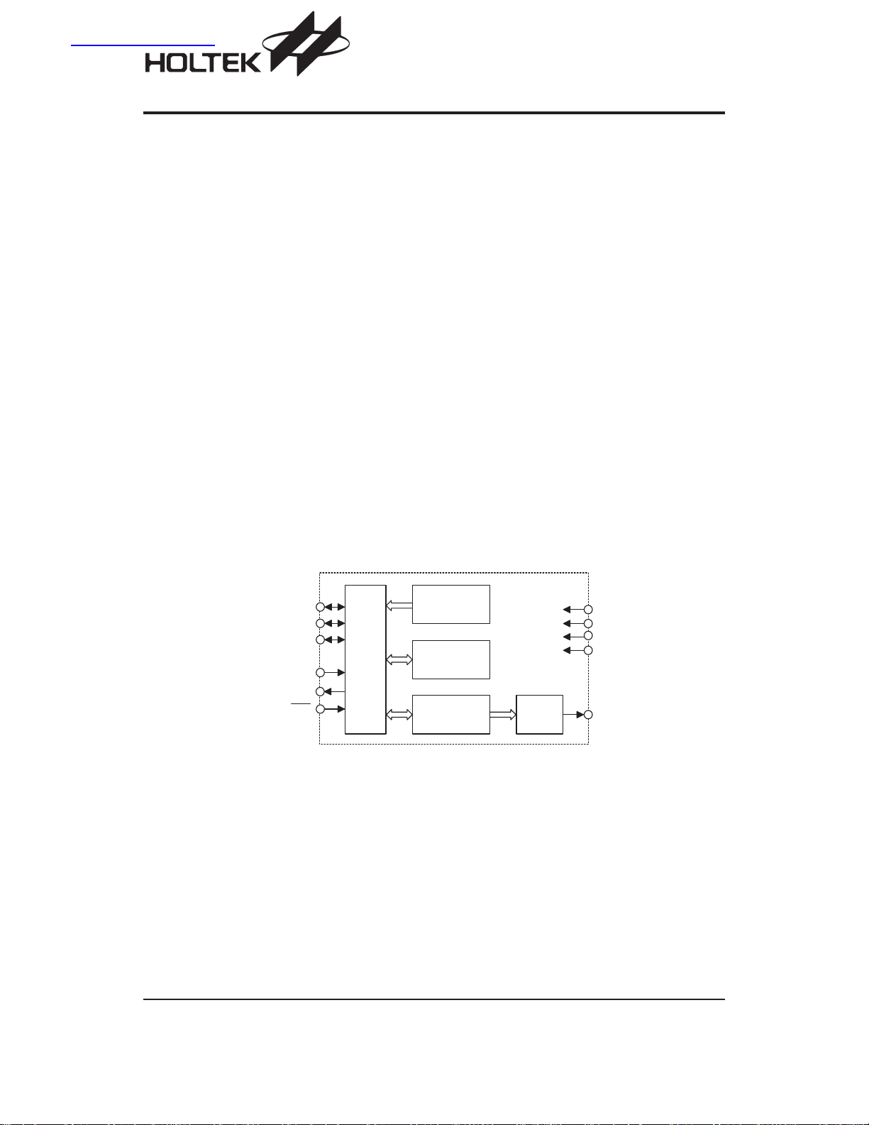
The HT36A3 has a built-in 8-bit microprocessor which
programs the synthesizer to generate the melody by
setting the special register from 20H~2AH. A HALT fea
ture is provided to reduce power consumption.
-
Block Diagram
P A 0 ~ P A 7
P B 0 ~ P B 7
P C 0 ~ P C 3
O S C 1
O S C 2
R E S
8 - B i t
M C U
3 2 K´1 6 - b i t
R O M
2 0 8
8
´
R A M
M u l t i p l i e r / P h a s e
G e n e r a l
1 6 - B i t
D A C
V D D
V S S
V D D A
V S S A
A U D
Rev. 1.00 1 June 30, 2003
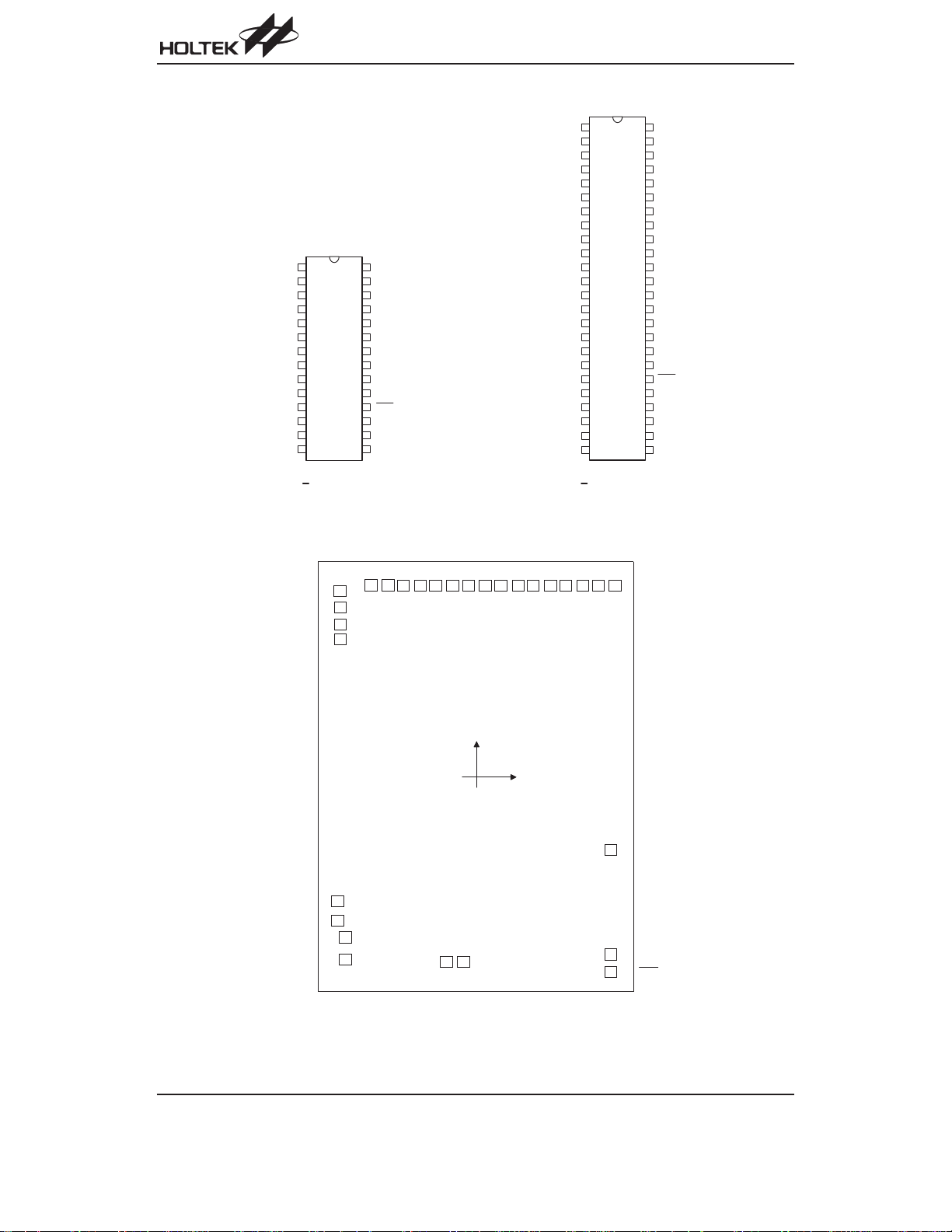
Pin Assignment
V S S A
V D D
V D D A
T E S T
A U D
P A 4
P A 5
P A 6
P A 7
N C
N C
N C
V S S
N C
1
2
3
4
5
6
7
8
9
1 0
1 1
1 2
1 3
1 4
H T 3 6 A 3
2 8 S O P - A
HT36A3
P A 4
1
P A 5
2
P A 6
3
P A 7
4
P B 0
5
P B 1
6
P B 2
7
P B 3
8
P B 4
9
P B 5
V S S A
V D D
V D D A
1 0
P B 6
1 1
P B 7
1 2
N C
1 3
N C
1 4
V S S
1 5
1 6
1 7
1 8
N C
1 9
N C
2 0
N C
2 1
N C
2 2
N C
2 3
N C
2 4
2 8
P A 3
2 7
P A 2
2 6
P A 1
2 5
P A 0
2 4
N C
2 3
N C
2 2
O S C 2
2 1
N C
2 0
O S C 1
1 9
N C
1 8
R E S
1 7
N C
1 6
N C
1 5
N C
H T 3 6 A 3
4 8 S S O P - A
P A 3
4 8
P A 2
4 7
P A 1
4 6
P A 0
4 5
P C 3
4 4
P C 2
4 3
P C 1
4 2
P C 0
4 1
N C
4 0
N C
3 9
N C
3 8
N C
3 7
N C
3 6
N C
3 5
O S C 2
3 4
O S C 1
3 3
N C
3 2
N C
3 1
R E S
3 0
N C
2 9
N C
2 8
N C
2 7
A U D
2 6
T E S T
2 5
Pad Assignment
V S S
V S S A
V D D
V D D A
P B 4
P B 5
P B 6
P B 7
P C 3
P C 2
P C 1
P B 3
P B 2
P B 1
P B 0
P A 7
P A 6
P A 5
P A 4
P A 3
P A 2
P A 1
P A 0
2 9
2 8
1
2
3
4
2 7 2 6
2 4
2 5
2 3 2 2
1 9
2 1
1 8 1 7
2 0
P C 0
1 4
1 5
1 6
( 0 , 0 )
1 3
O S C 2
5
6
7
1 2
8
9
1 0
A U D
T E S T
O S C 1
1 1
R E S
Chip size: 83 ´ 111 (mil)
2
* The IC substrate should be connected to VSS in the PCB layout artwork.
Rev. 1.00 2 June 30, 2003

Pad Coordinates
Pad No. X Y Pad No. X Y
1
2
3
4
5
6
7
8
9
10
11 875.950
12 875.950
13 875.950
14 901.500 1240.150 29
15 793.900 1240.150
-879.100
-879.100
-879.100
-879.100
-898.600 -805.050
-898.600 -931.910
-847.650 -1041.910
-847.650 -1180.350
-193.090 -1200.600
-81.290 -1200.600
1202.400 16 693.900 1240.150
1097.100 17 583.300 1240.150
986.500 18 483.300 1240.150
886.500 19 372.700 1240.150
20 272.700 1240.150
21 162.100 1240.150
22 62.100 1240.150
-1262.274
-1149.626
-471.774
23
24
25
26
27
28
-48.500
-148.500
-259.100
-359.100
-469.700
-569.700
-680.300
Pad Description
I
I
Internal
Connection
Pull-High
or None
Pull-High
or None
Pull-High
or None
¾
¾
¾
Function
Bidirectional 8-bit Input/Output port
Bidirectional 8-bit Input/Output port
Bidirectional 8-bit Input/Output port
Negative power supply, ground
Negative power supply of DAC, ground
Digital power supply
DAC power supply
Audio output
No connection (open)
Reset input, active low (no pull-high)
OSC1 and OSC2 are connected to an RC network or a crystal (by mask op
tion) for the internal system clock. In the case of RC operation, OSC2 is the
output terminal for 1/8 system clock. The system clock may come from the
crystal, the two pins cannot be floating.
Pad Name I/O
PA0~PA7 I/O
PB0~PB7 I/O
PC0~PC3 I/O
VSS
VSSA
VDD
VDDA
AUD O
TEST
RES
OSC1
OSC2
¾¾
¾¾
¾¾
¾¾
¾¾
O
HT36A3
1240.150
1240.150
1240.150
1240.150
1240.150
1240.150
1240.150
-
Rev. 1.00 3 June 30, 2003
HT36A3
Absolute Maximum Ratings
Supply Voltage .............................VSS-0.3V to VSS+6V
Input Voltage .............................V
3V to VDD+0.3V
SS-0.
Note: These are stress ratings only. Stresses exceeding the range specified under ²Absolute Maximum Ratings² may
cause substantial damage to the device. Functional operation of this device at other conditions beyond those
listed in the specification is not implied and prolonged exposure to extreme conditions may affect device reliabil
ity.
Storage Temperature ...........................-50°Cto125°C
Operating Temperature ..........................-25°Cto70°C
-
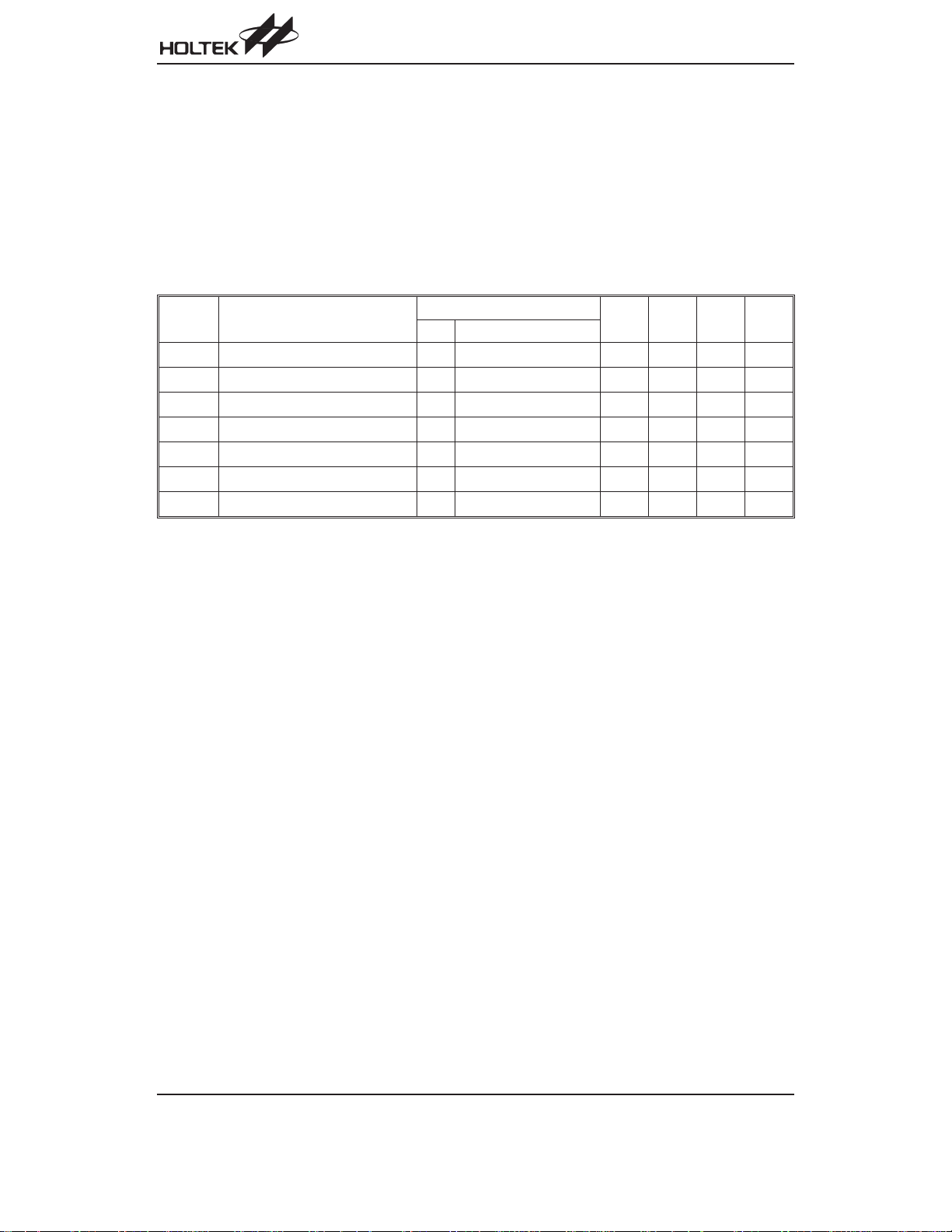
D.C. Characteristics
Symbol Parameter
V
I
I
I
I
V
V
DD
DD
STB
OH
OL
IH
IL
Operating Voltage
Operating Current 4.5V
Standby Current (WDT Disabled) 4.5V No load, System HALT
I/O Ports Source Current 4.5V
I/O Ports Sink Current 4.5V
Input High Voltage for I/O Ports 4.5V
Input Low Voltage for I/O Ports 4.5V
Test Conditions
V
DD
Conditions
¾¾
No load, f
=4.5V
V
OH
=0.5V
V
OL
OSC
=8MHz
¾
¾
Ta=25°C
Min. Typ. Max. Unit
2.2 4.5 5.5 V
¾
¾
23
23
0.8V
0
816mA
13
¾
¾
V
¾
DD
¾
DD
0.2V
DD
mA
mA
mA
V
V
Rev. 1.00 4 June 30, 2003

Application Circuit
HT36A3
V
D D
1 0
W
1 0 0 k
0 . 1mF
O S C 1
V D D
V D D A
P A 0 ~ P A 7
4 7mF
0 . 1mF
P B 0 ~ P B 7
V
P C 0 ~ P C 3
1 k
A U D
V
D D
W
D D
S P K
8
W
7 5 0
W
W
R E S
V S S A
V S S
H T 3 6 A 3
V
D D
1 0
W
V D D V D D A
4 7mF
0 . 1mF
1 0 0 k
0 . 1mF
8 M H z
O S C 1
O S C 2
P A 0 ~ P A 7
P B 0 ~ P B 7
P C 0 ~ P C 3
V
D D
4 7mF
I N
H T 8 2 V 7 3 3
5
C E
V D D
8
O U T N
V S S
1
7
O U T P
4
S P K
8
W
A U D
2 0 k
W
V
D D
W
R E S
V S S A
1 0
F
0 . 1
m
2
V r e f
3
F
m
V S S
H T 3 6 A 3
Rev. 1.00 5 June 30, 2003

Package Information
28-pin SOP (300mil) Outline Dimensions
HT36A3
2 8
A
1
C
C '
D
E
Symbol
A 394
B 290
C14
C¢
D92
E
F4
G32
H4
1 5
B
1 4
G
H
F
a
Dimensions in mil
Min. Nom. Max.
¾
¾
¾
697
¾
¾
¾
50
¾¾
¾
¾
a 0°¾10°
419
300
20
713
104
¾
38
12
Rev. 1.00 6 June 30, 2003

48-pin SSOP (300mil) Outline Dimensions
HT36A3
4 8
A
1
C
C '
D
E
Symbol
Min. Nom. Max.
A 395
B 291
C8
C¢
613
D85
E
¾
F4
G25
H4
2 5
B
2 4
F
Dimensions in mil
¾
¾
¾
¾
¾
25
¾
¾
¾
G
a
a 0°¾8°
H
420
299
12
637
99
¾
10
35
12
Rev. 1.00 7 June 30, 2003

Product Tape and Reel Specifications
Reel Dimensions
HT36A3
T 2
A
B
T 1
D
SOP 28W (300mil)
Symbol Description Dimensions in mm
A Reel Outer Diameter
B Reel Inner Diameter
C Spindle Hole Diameter
D Key Slit Width
T1 Space Between Flange
T2 Reel Thickness
330±1.0
62±1.5
13.0+0.5
2.0±0.5
24.8+0.3
30.2±0.2
C
-0.2
-0.2
SSOP 48W
Symbol Description Dimensions in mm
A Reel Outer Diameter
B Reel Inner Diameter
C Spindle Hole Diameter
D Key Slit Width
T1 Space Between Flange
T2 Reel Thickness
330±1.0
100±0.1
13.0+0.5
-0.2
2.0±0.5
32.2+0.3
-0.2
38.2±0.2
Rev. 1.00 8 June 30, 2003

Carrier Tape Dimensions
HT36A3
D
E
F
PD 1
P 1P 0
W
A 0
B 0
C
SOP 28W (300mil)
Symbol Description Dimensions in mm
W Carrier Tape Width
P Cavity Pitch
E Perforation Position
F Cavity to Perforation (Width Direction)
24.0±0.3
12.0±0.1
1.75±0.1
11.5±0.1
D Perforation Diameter 1.5+0.1
D1 Cavity Hole Diameter 1.5+0.25
P0 Perforation Pitch
P1 Cavity to Perforation (Length Direction)
A0 Cavity Length
B0 Cavity Width
K0 Cavity Depth
t Carrier Tape Thickness
4.0±0.1
2.0±0.1
10.85±0.1
18.34±0.1
2.97±0.1
0.35±0.01
C Cover Tape Width 21.3
t
K 0
Rev. 1.00 9 June 30, 2003

HT36A3
D
E
F
PD 1
P 1P 0
W
A 0
B 0
C
SSOP 48W
Symbol Description Dimensions in mm
W Carrier Tape Width
P Cavity Pitch
E Perforation Position
F Cavity to Perforation (Width Direction)
32.0±0.3
16.0±0.1
1.75±0.1
14.2±0.1
D Perforation Diameter 2.0 Min.
D1 Cavity Hole Diameter 1.5+0.25
P0 Perforation Pitch
P1 Cavity to Perforation (Length Direction)
A0 Cavity Length
B0 Cavity Width
K1 Cavity Depth
K2 Cavity Depth
t Carrier Tape Thickness
4.0±0.1
2.0±0.1
12.0±0.1
16.20±0.1
2.4±0.1
3.2±0.1
0.35±0.05
C Cover Tape Width 25.5
t
K 1
K 2
Rev. 1.00 10 June 30, 2003

Holtek Semiconductor Inc. (Headquarters)
No.3, Creation Rd. II, Science Park, Hsinchu, Taiwan
Tel: 886-3-563-1999
Fax: 886-3-563-1189
http://www.holtek.com.tw
HT36A3
Holtek Semiconductor Inc. (Taipei Sales Office)
4F-2, No. 3-2, YuanQu St., Nankang Software Park, Taipei 115, Taiwan
Tel: 886-2-2655-7070
Fax: 886-2-2655-7373
Fax: 886-2-2655-7383 (International sales hotline)
Holtek Semiconductor Inc. (Shanghai Sales Office)
7th Floor, Building 2, No.889, Yi Shan Rd., Shanghai, China 200233
Tel: 021-6485-5560
Fax: 021-6485-0313
http://www.holtek.com.cn
Holtek Semiconductor Inc. (Shenzhen Sales Office)
43F, SEG Plaza, Shen Nan Zhong Road, Shenzhen, China 518031
Tel: 0755-8346-5589
Fax: 0755-8346-5590
ISDN: 0755-8346-5591
Holtek Semiconductor Inc. (Beijing Sales Office)
Suite 1721, Jinyu Tower, A129 West Xuan Wu Men Street, Xicheng District, Beijing, China 100031
Tel: 010-6641-0030, 6641-7751, 6641-7752
Fax: 010-6641-0125
Holmate Semiconductor, Inc. (North America Sales Office)
46712 Fremont Blvd., Fremont, CA 94538
Tel: 510-252-9880
Fax: 510-252-9885
http://www.holmate.com
Copyright Ó 2003 by HOLTEK SEMICONDUCTOR INC.
The information appearing in this Data Sheet is believed to be accurate at the time of publication. However, Holtek as
sumes no responsibility arising from the use of the specifications described. The applications mentioned herein are used
solely for the purpose of illustration and Holtek makes no warranty or representation that such applications will be suitable
without further modification, nor recommends the use of its products for application that may present a risk to human life
due to malfunction or otherwise. Holtek¢s products are not authorized for use as critical components in life support devices
or systems. Holtek reserves the right to alter its products without prior notification. For the most up-to-date information,
please visit our web site at http://www.holtek.com.tw.
-
Rev. 1.00 11 June 30, 2003
 Loading...