

Page 1
8-Bit Music Synthesizer MCU
Features
·
Operating voltage: 2.4V~5.0V
·
Operating frequency: 3.58MHz~12MHz (typ. 8MHz)
·
20 bidirectional I/O lines
·
Two 8-bitprogrammable timer with 8 stage prescaler
·
Watchdog Timer
·
Built-in 8-bit MCU with 208´8 bits RAM
·
Built-in 64K´16-bit ROM for program/data shared
·
Mono output
·
High D/A converter resolution: 16 bits
·
Polyphonic up to 8 notes
·
Independent volume mix can be assigned to each
sound component
General Description
The HT36A2 is an 8-bit high performance RISC-like
microcontroller specifically designed for music applica
tions. It provides an 8-bit MCU and a 8 channel
wavetable synthesizer. The program ROM is composed
of both program control codes and wavetable voice
codes, and can be easily programmed.
HT36A2
·
Sampling rate of 25kHz as 6.4MHz for system
frequency
·
Eight-level subroutine nesting
·
HALT function and wake-up feature to reduce power
consumption
·
Bit manipulation instructions
·
16-bit table read instructions
·
63 powerful instructions
·
All instructions in 1 or 2 machine cycles
·
28-pin SOP, 48-pin SSOP package
The HT36A2 has a built-in 8-bit microprocessor which
programs the synthesizer to generate the melody by
setting the special register from 20H~2AH. A HALT fea
ture is provided to reduce power consumption.
-
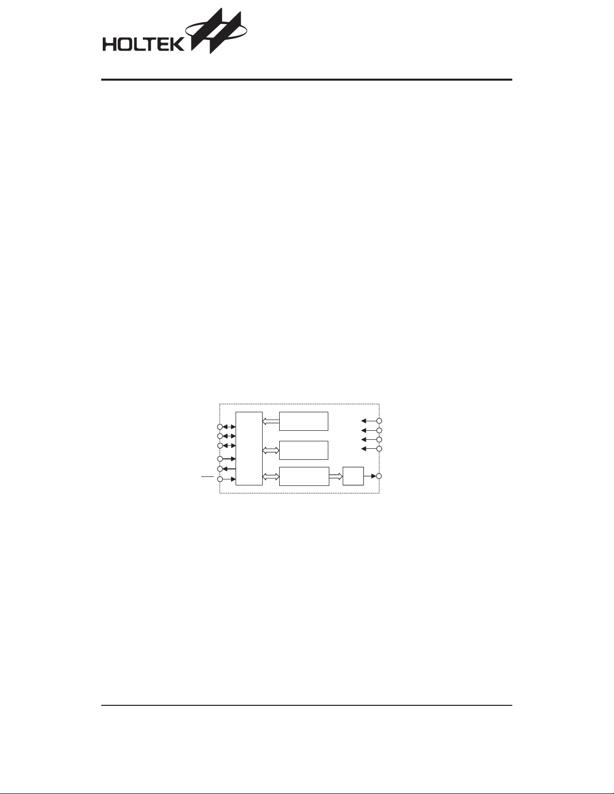
Block Diagram
P A 0 ~ P A 7
P B 0 ~ P B 7
P C 0 ~ P C 3
O S C 1
O S C 2
R E S
8 - B i t
M C U
6 4 K´1 6 - b i t
R O M
2 0 8´8
R A M
M u l t i p l i e r / P h a s e
G e n e r a l
1 6 - B i t
D A C
V D D
V S S
V D D A
V S S A
A U D
Rev. 1.00 1 June 19, 2003
Page 2
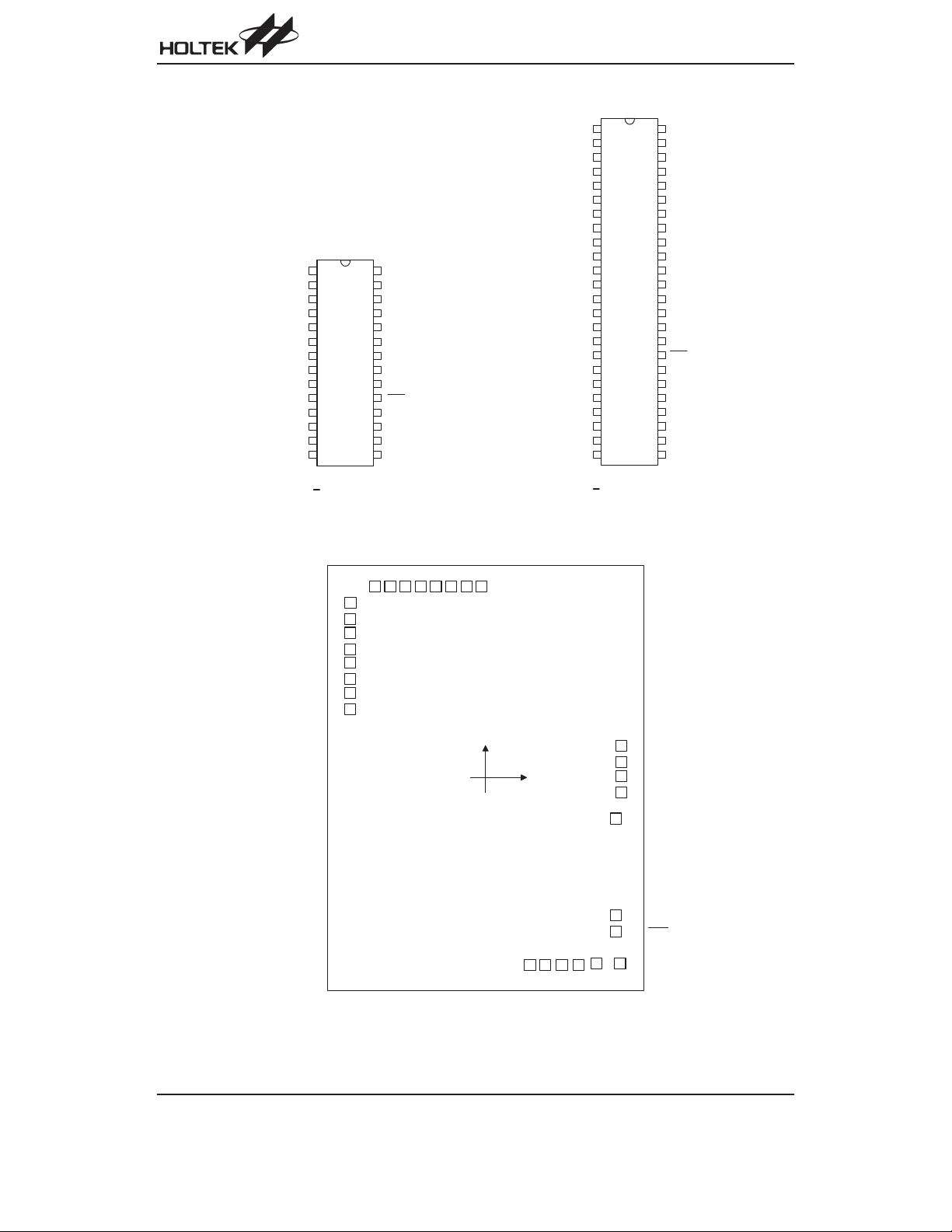
Pin Assignment
A U D
T E S T
P A 4
P A 5
P A 6
P A 7
N C
N C
N C
N C
N C
N C
N C
N C
1
2
3
4
5
6
7
8
9
1 0
1 1
1 2
1 3
1 4
H T 3 6 A 2
2 8 S O P - A
HT36A2
P A 4
1
P A 5
2
P A 6
3
P A 7
4
N C
5
P B 0
6
P B 1
7
P B 2
8
P B 3
9
P B 4
1 0
2 8
P A 3
2 7
P A 2
2 6
P A 1
2 5
P A 0
2 4
N C
2 3
N C
2 2
O S C 2
2 1
N C
2 0
O S C 1
1 9
R E S
1 8
V S S
1 7
V S S A
1 6
V D D
1 5
V D D A
P B 5
1 1
P B 6
1 2
P B 7
1 3
N C
1 4
N C
1 5
N C
1 6
N C
1 7
N C
1 8
N C
1 9
N C
2 0
N C
2 1
N C
2 2
N C
2 3
N C
2 4
H T 3 6 A 2
4 8 S S O P - A
P A 3
4 8
P A 2
4 7
P A 1
4 6
P A 0
4 5
N C
4 4
N C
4 3
N C
4 2
N C
4 1
N C
4 0
N C
3 9
P C 0
3 8
P C 1
3 7
P C 2
3 6
P C 3
3 5
O S C 2
3 4
O S C 1
3 3
R E S
3 2
N C
3 1
V S S
3 0
V S S A
2 9
V D D
2 8
V D D A
2 7
T E S T
2 6
A U D
2 5
Pad Assignment
P B 0
P B 1
P B 2
P B 3
P B 4
P B 5
P B 6
P B 7
P A 4
P A 3
P A 7
P A 6
2 9
2 8
1
2
3
4
5
6
7
8
P A 2
P A 1
P A 5
2 6
2 7
2 5
P A 0
2 2
2 4
2 3
P C 0
2 1
P C 1
( 0 , 0 )
1 0
9
1 1
2 0
P C 2
1 9
P C 3
1 8
O S C 2
1 7
O S C 1
1 6
1 5
R E S
1 3 1 4
1 2
V D D A
T E S T
V D D
V S S A
A U D
V S S
Chip size: 87.2 ´ 118.3 (mil)
* The IC substrate should be connected to VSS in the PCB layout artwork.
Rev. 1.00 2 June 19, 2003
Page 3

HT36A2
Pad Coordinates
Pad No. X Y Pad No. X Y
1
2
3
4
5
6
7
8
9 301.450
10 413.250
11 526.890
12 636.250
13 761.700
14 924.250
15 899.200
-939.550
-939.550
-939.550
-939.550
-939.550
-939.550
-939.550
-939.550
1222.175 16 899.200
1111.575 17 899.200
1011.575 18 938.800
900.975 19 938.800 9.925
800.975 20 938.800 109.925
690.375 21 938.800 220.525
590.375 22
479.775 23
-1303.400
-1303.400
-1303.400
-1303.400
-1296.750
-1296.750
-1078.450
24
25
26
27
28
29
-26.300
-136.900
-236.900
-347.500
-447.500
-558.100
-658.100
-768.700
Pad Description
Pad Name I/O
PB0~PB7 I/O
AUD O
TEST
VDDA
VDD
VSSA
VSS
RES
OSC1
OSC2
PC0~PC3 I/O
PA0~PA7 I/O
Internal
Connection
Pull-High
or None
¾
¾¾
¾¾
¾¾
¾¾
¾¾
I
I
O
¾
¾
Pull-High
or None
Pull-High
or None
Function
Bidirectional 8-bit Input/Output port
Audio output for driving a external transistor or for driving HT82V733
No connection (open)
DAC power supply
Positive power supply
Negative power supply of DAC, ground
Negative power supply, ground
Reset input, active low
OSC1 and OSC2 are connected to an RC network or a crystal (by mask option)
for the internal system clock. In the case of RC operation, OSC2 is the output
terminal for 1/8 system clock. The system clock may come from the crystal, the
two pins cannot be floating.
Bidirectional 4-bit Input/Output port
Bidirectional 8-bit Input/Output port, wake-up by mask option
Unit: mm
-965.126
-287.274
-100.675
1336.775
1336.775
1336.775
1336.775
1336.775
1336.775
1336.775
1336.775
Absolute Maximum Ratings
Supply Voltage .............................VSS-0.3V to VSS+6V
Input Voltage .............................V
Note: These are stress ratings only. Stresses exceeding the range specified under ²Absolute Maximum Ratings² may
cause substantial damage to the device. Functional operation of this device at other conditions beyond those
listed in the specification is not implied and prolonged exposure to extreme conditions may affect device reliabil
ity.
Rev. 1.00 3 June 19, 2003
3V to VDD+0.3V
SS-0.
Storage Temperature ...........................-50°Cto125°C
Operating Temperature ..........................-25°Cto70°C
-
Page 4
HT36A2
D.C. Characteristics
Symbol Parameter
V
I
I
I
I
R
V
V
V
V
DD
DD
STB
OL
OH
PH
IH1
IL1
IH2
IL2
Operating Voltage
Operating Current 5V
Standby Current (WDT Disabled) 5V
I/O Ports Sink Current 5V
I/O Ports Source Current 5V
Pull-High Resistance of I/O Ports 5V
Input High Voltage for I/O Ports 5V
Input Low Voltage for I/O Ports 5V
Input High Voltage (RES)5V
Input Low Voltage (RES)5V
A.C. Characteristics
Symbol Parameter
MCU interface
f
OSC
f
SYS
t
WDT
t
RES
System Frequency 5V 8MHz crystal
System Clock 5V
Watchdog Time-Out Period (RC)
External Reset Low Pulse Width
Test Conditions
V
DD
Conditions
¾¾
No load, f
OSC
=8MHz
No load
System HALT
=0.5V
V
OL
=4.5V
V
OH
=0V
V
IL
¾
¾
Min. Typ. Max. Unit
2.4 3 5 V
¾
¾
816mA
1
9.7 16.2
-5.2 -8.7 ¾
11 22 44
3.5
¾
0
¾
¾¾4¾
¾¾
Test Conditions
V
DD
Conditions
Min. Typ. Max. Unit
¾
¾
Without WDT prescaler 9 17 35 ms
¾
¾¾
2.5
8
4
¾
1
¾¾ms
Ta=25°C
¾mA
mA
¾
mA
kW
5V
1.5 V
V
¾
¾
V
MHz
8 MHz
Characteristics Curves
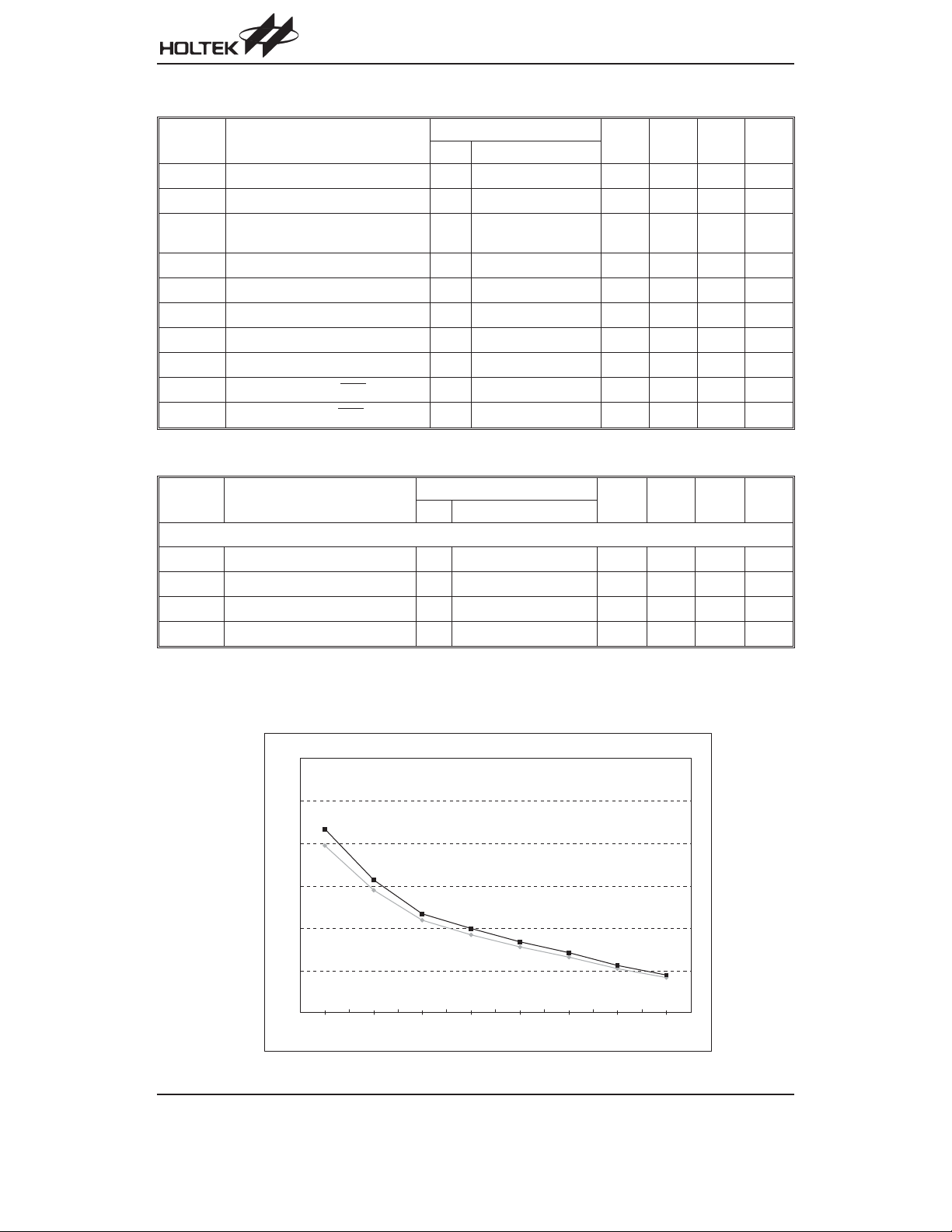
R vs F Characteristics Curve
1 4
1 2
1 0
8
F r e q u e n c y ( M H z )
6
4
2
1 2 0 1 5 0 1 8 0 2 0 0 2 2 0 2 4 0 2 7 0 3 0 0
Rev. 1.00 4 June 19, 2003
H T 3 6 A 2 R v s . F C h a r t
)
R ( k
W
3 . 0 V
4 . 5 V
Page 5
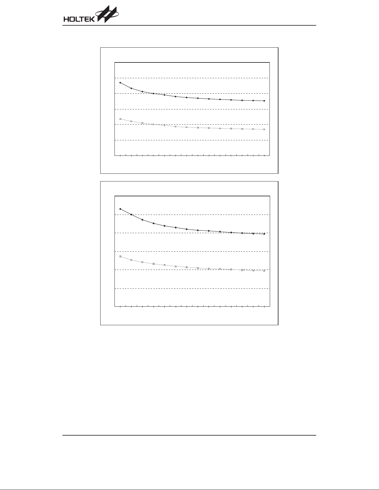
V vs F Characteristics Curve
HT36A2
1 0
9
8
7
F r e q u e n c y ( M H z )
6
5
4
2 . 4 2 . 6 2 . 8 3 3 . 2 3 . 4 3 . 6 3 . 8 4 4 . 2 4 . 4 4 . 6 4 . 8 5
1 0
9
8
H T 3 6 A 2 V v s . F C h a r t ( F o r 3 . 0 V )
( V )
D D
V
H T 3 6 A 2 V v s . F C h a r t ( F o r 4 . 5 V )
1 5 5 k
2 0 0 k
1 4 5 k
/ 8 M H z
W
/ 6 M H z
W
/ 8 M H z
W
7
F r e q u e n c y ( M H z )
6
5
4
2 . 4 2 . 6 2 . 8 3 3 . 2 3 . 4 3 . 6 3 . 8 4 4 . 2 4 . 4 4 . 6 4 . 8 5
V
( V )
D D
1 9 0 k
/ 6 M H z
W
Rev. 1.00 5 June 19, 2003
Page 6
Function Description
Execution Flow
The system clock for the HT36A2 is derived from either
a crystal or an RC oscillator. The oscillator frequency di
vided by 2 is the system clock for the MCU and it is inter
nally divided into four non-overlapping clocks. One
instruction cycle consists of four system clock cycles.
Instruction fetching and execution are pipelined in such
a way that a fetch takes one instruction cycle while de
coding and execution takes the next instruction cycle.
However, the pipelining scheme causes each instruc
tion to effectively execute in one cycle. If an instruction
changes the program counter, two cycles are required
to complete the instruction.
Program Counter - PC
The 13-bit program counter (PC) controls the sequence
in which the instructions stored in program ROM are ex
ecuted and its contents specify a maximum of 8192 ad
dresses for each bank.
After accessing a program memory word to fetch an in
struction code, the contents of the program counter are
incremented by one. The program counter then points
to the memory word containing the next instruction
code.
When executing a jump instruction, conditional skip ex
ecution, loading PCL register, subroutine call, initial re
set, internal interrupt, external interrupt or return from
-
subroutine, the PC manipulates the program transfer by
-
loading the address corresponding to each instruction.
The conditional skip is activated by instruction. Once the
condition is met, the next instruction, fetched during the
current instruction execution, is discarded and a dummy
-
cycle replaces it to retrieve the proper instruction. Other
wise proceed with the next instruction.
-
The lower byte of the program counter (PCL) is a read
able and writeable register (06H). Moving data into the
PCL performs a short jump. The destination will be
within 256 locations.
Once a control transfer takes place, an additional
dummy cycle is required.
-
-
Program ROM
HT36A2 provides 16 address lines WA[15:0] to read the
-
Program ROM which is up to 1M bits, and is commonly
used for the wavetable voice codes and the program
memory. It provides two address types, one type is for
program ROM, which is addressed by a bank pointer
PF2~0 and a 13-bit program counter PC 12~0; and the
HT36A2
-
-
-
-
S y s t e m C l o c k o f M C U
( S y s t e m C l o c k / 2 )
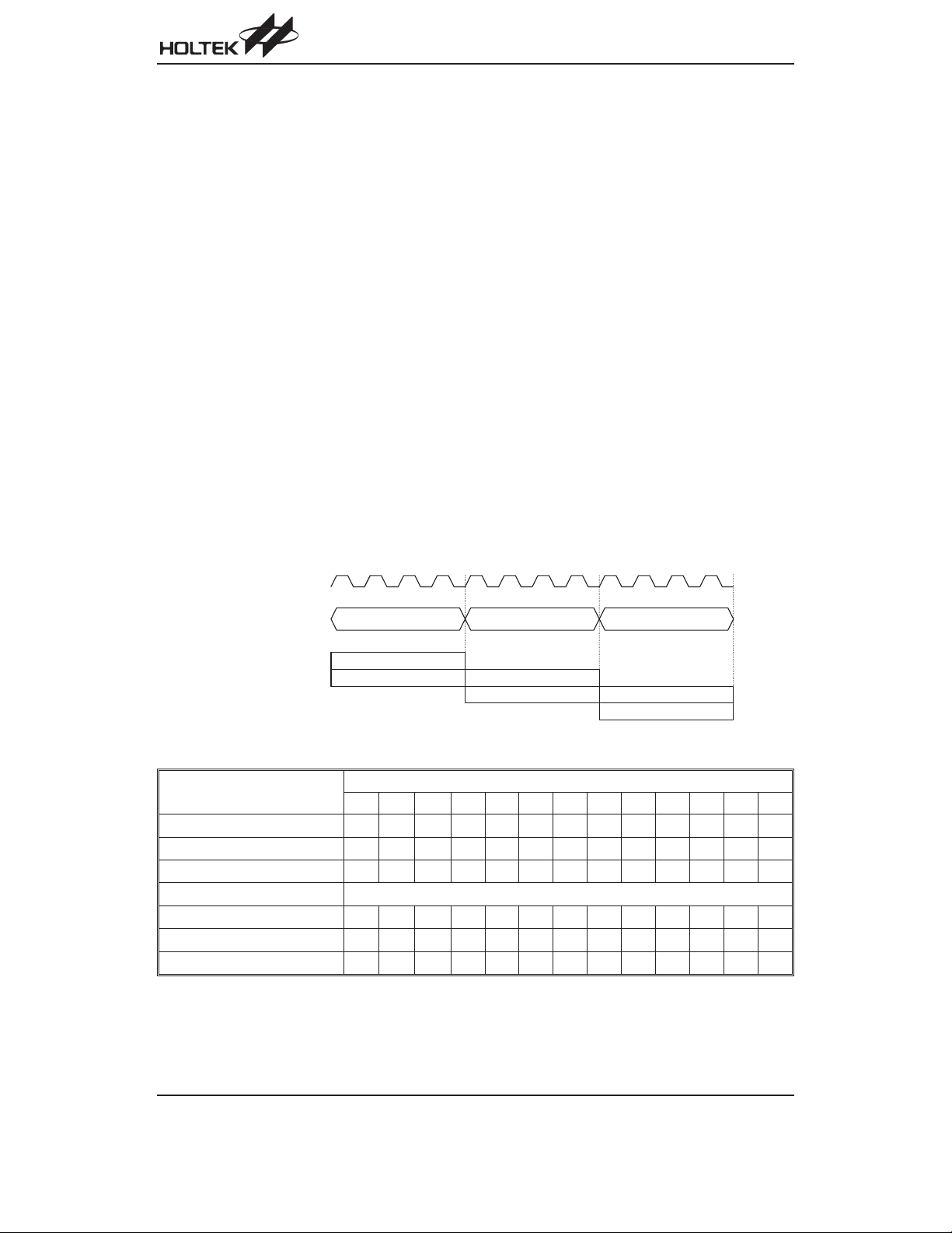
T 1 T 2 T 3 T 4 T 1 T 2 T 3 T 4 T 1 T 2 T 3 T 4
P C
P C P C + 1 P C + 2
F e t c h I N S T ( P C )
E x e c u t e I N S T ( P C - 1 )
F e t c h I N S T ( P C + 1 )
E x e c u t e I N S T ( P C )
F e t c h I N S T ( P C + 2 )
E x e c u t e I N S T ( P C + 1 )
Execution flow
Mode
*12 *11 *10 *9 *8 *7 *6 *5 *4 *3 *2 *1 *0
Program Counter
Initial Reset 0 0 0 0000000000
Timer/Event Counter 0 Overflow 0 0 0 0000001000
Timer/Event Counter 1 Overflow 0 0 0 0000001100
Skip PC+2
Loading PCL *12 *11 *10 *9 *8 @7 @6 @5 @4 @3 @2 @1 @0
Jump, Call Branch #12 #11 #10 #9 #8 #7 #6 #5 #4 #3 #2 #1 #0
Return From Subroutine S12 S11 S10 S9 S8 S7 S6 S5 S4 S3 S2 S1 S0
Program counter
Note: *12~*0: Bits of Program Counter
@7~@0: Bits of PCL
S12~S0: Bits of Stack Register
@7~@0: Bits of PCL
#12~#0: Bits of Instruction Code
Rev. 1.00 6 June 19, 2003
Page 7
HT36A2
other type is for wavetable code, which is addressed by
the start address ST11~0. On the program type,
13
WA15~0= PF2~0 ´ 2
ROM type, WA15~0=ST11~0 ´ 2
+ PC12~0. On the wave table
5
.
Program Memory - ROM
The program memory is used to store the program in
structions which are to be executed. It also contains
data, table, and interrupt entries, and is organized into
8192´16 bits, addressed by the bank pointer, program
counter and table pointer.
Certain locations in the program memory of each bank
are reserved for special usage:
·
Location 000H on bank0
This area is reserved for the initialization program. Af
ter chip reset, the program always begins execution at
location 000H on bank0.
·
Location 008H
This area is reserved for the Timer Counter 0 interrupt
service program on each bank. If timer interrupt results
from a timer counter 0 overflow, and if the interrupt is
enabled and the stack is not full, the program begins ex
ecution at location 008H corresponding to its bank.
·
Location 00CH
This area is reserved for the Timer Counter 1 interrupt
service program on each bank. If a timer interrupt results from a Timer Counter 1 overflow, and if the interrupt is enabled and the stack is not full, the program
begins execution at location 00CH corresponding to
its bank.
·
Table location
Any location in the ROM space can be used as
look-up tables. The instructions TABRDC [m] (the current page, 1 page=256 words) and TABRDL [m] (the
last page) transfer the contents of the lower-order
byte to the specified data memory, and the
higher-order byte to TBLH (08H). Only the destination
of the lower-order byte in the table is well-defined, the
higher-order byte of the table word are transferred to
the TBLH. The Table Higher-order byte register
(TBLH) is read only. The Table Pointer (TBLP) is a
read/write register (07H), which indicates the table lo
cation. Before accessing the table, the location must
be placed in TBLP. The TBLH is read only and cannot
be restored. If the main routine and the ISR (Interrupt
0 0 0 0 H
0 0 0 8 H
0 0 0 C H
-
n 0 0 H
n F F H
1 F F F H
-
D e v i c e i n i t i a l i z a t i o n p r o g r a m
T i m e r C o u n t e r 0 i n t e r r u p t s u b r o u t i n e
T i m e r C o u n t e r 1 i n t e r r u p t s u b r o u t i n e
L o o k - u p t a b l e ( 2 5 6 w o r d s )
L o o k - u p t a b l e ( 2 5 6 w o r d s )
1 6 b i t s
N o t e : n r a n g e s f r o m 0 0 t o 1 F .
Program memory for each bank
Service Routine) both employ the table read instruc
tion, the contents of the TBLH in the main routine are
likely to be changed by the table read instruction used
in the ISR. Errors can occur. In this case, using the ta
ble read instruction in the main routine and the ISR si
-
multaneously should be avoided. However, if the
table read instruction has to be applied in both the
main routine and the ISR, the interrupt should be dis
abled prior to the table read instruction. It will not be
enabled until the TBLH has been backed up. All table
related instructions need 2 cycles to complete the operation. These areas may function as normal program
memory depending upon user requirements.
·
Bank pointer
The program memory is organized into 8 banks and
each bank into 8192 ´ 16 bits of program ROM.
PF[2~0] is used as the bank pointer. After an instruction has been executed to write data to the PF register
to select a different bank, note that the new bank will
not be selected immediately. It is not until the following
instruction has completed execution that the bank will
be actually selected. It should be note that the PF reg
ister hasto becleared before setting to output mode.
Wavetable ROM
The ST[11~0] is used to defined the start address of
-
each sample on the wavetable and read the waveform
data from the location. HT36A2 provides 16 output ad
dress lines from WA[15~0], the ST[11~0] is used to lo
P r o g r a m
R O M
-
-
-
-
-
-
-
Instruction(s)
*12 *11 *10 *9 *8 *7 *6 *5 *4 *3 *2 *1 *0
Table Location
TABRDC [m] P12 P11 P10 P9 P8 @7 @6 @5 @4 @3 @2 @1 @0
TABRDL [m] 11111@7@6@5@4@3@2@1@0
Table location
Note: *12~*0: Bits of table location
P12~P8: Bits of current Program Counter
@7~@0: Bits of table pointer
Rev. 1.00 7 June 19, 2003
Page 8

HT36A2
cate the major 16 bits i.e. WA[15:5] and the undefined
data from WA[4~0] is always set to 00000b. So the start
address of each sample have to be located at a multiple
of 32. Otherwise, the sample will not be read out cor
rectly because it has a wrong starting code.
Stack Register - Stack
This is a special part of the memory which is used to
save the contents of the program counter (PC) only. The
stack is organized into 8 levels and is neither part of the
data nor part of the program space, and is neither read
able nor writeable. The activated level is indexed by the
stack pointer (SP) and is neither readable nor writeable.
At a subroutine call or interrupt acknowledgment, the
contents of the program counter are pushed onto the
stack. At the end of a subroutine or an interrupt routine,
signaled by a return instruction (RET or RETI), the pro
gram counter is restored to its previous value from the
stack. Aftera chip reset, the SP will point tothe top of the
stack.
If the stack is full and a non-masked interrupt takes
place, the interrupt request flag will be recorded but the
acknowledgment will be inhibited. When the stack
pointer is decremented (by RET or RETI), the interrupt
will be serviced. This feature prevents stack overflow al
lowing the programmer to use the structure more easily.
In a similar case, if the stack is full and a CALL is subsequently executed, a stack overflow occurs and the first
entry will be lost (only the most recent eight return address are stored).
Data Memory - RAM
The datamemory is designed with 256 ´ 8 bits. The data
memory is divided into three functional groups: special
function registers, wavetable function register, and gen
eral purpose data memory (208´8). Most of them are
read/write, but some are read only.
The special function registers include the Indirect Ad
dressing register 0 (00H), the Memory Pointer register 0
(MP0;01H), the Indirect Addressing register 1 (02H), the
Memory Pointer register 1 (MP1;03H), the Accumulator
(ACC;05H), the Program Counter Lower-byte register
(PCL;06H), the Table Pointer (TBLP;07H), the Table
Higher-order byte register (TBLH;08H), the Watchdog
Timer option Setting register (WDTS;09H), the Status
register (STATUS;0AH), the Interrupt Control register
(INTC;0BH), the Timer Counter 0 Lower-order byte reg
ister (TMR0L;0DH), the Timer Counter 0 Control regis
ter (TMR0C;0EH), the Timer Counter 1 Lower-order
byte register (TMR1L;10H), the Timer Counter 1 Control
register (TMR1C;11H), the I/O registers (PA;12H,
PB;14H, PC;16H) and the I/O control registers
(PAC;13H, PBC;15H, PCC;17H). The program ROM
bank select (PF;1CH). The DAC High byte (DAH;1DH).
The DAC low byte (DAL;1EH). The DAC control
(DAC;1FH). The wavetable function registers is defined
between 20H~2AH. The remaining space before the
30H is reserved for future expanded usage and reading
these locations will return the result 00H. The general
purpose data memory, addressed from 30H to FFH, is
-
used for data and control information under instruction
command.
I n d i r e c t A d d r e s s i n g R e g i s t e r 0
0 0 H
0 1 H
0 2 H
I n d i r e c t A d d r e s s i n g R e g i s t e r 1
0 3 H
-
0 4 H
0 5 H
0 6 H
0 7 H
0 8 H
0 9 H
0 A H
-
0 B H
0 C H
0 D H
0 E H
0 F H
1 0 H
1 1 H
1 2 H
1 3 H
-
1 4 H
1 5 H
1 6 H
1 7 H
1 8 H
1 9 H
1 A H
1 B H
1 C H
1 D H
1 E H
-
1 F H
2 0 H
2 1 H
F r e q u e n c y n u m b e r h i g h b y t e
2 2 H
-
F r e q u e n c y n u m b e r l o w b y t e
2 3 H
2 4 H
2 5 H
2 6 H
2 7 H
2 8 H
2 9 H
2 A H
2 B H
R e p e a t n u m b e r h i g h b y t e
M P 0
M P 1
A C C
P C L
T B L P
T B L H
W D T S
S T A T U S
I N T C
T M R 0 L
T M R 0 C
T M R 1 L
T M R 1 C
P A
P A C
P B
P B C
P C
P C C
P F
D A C h i g h b y t e
D A C l o w b y t e
D A C c o n t r o l
C h a n n e l n u m b e r s e l e c t
S t a r t a d d r e s s h i g h b y t e
S t a r t a d d r e s s l o w b y t e
R e p e a t n u m b e r l o w b y t e
V o l u m e c o n t r o l h i g h
V o l u m c o n t r o l l o w
S p e c i a l P u r p o s e
D A T A M E M O R Y
W a v e t a b l e F u n c t i o n
R e g i s t e r
-
-
2 F H
3 0 H
G e n e r a l P u r p o s e
D A T A M E M O R Y
( 2 0 8 B y t e s )
F F H
: U n u s e d .
R e a d a s " 0 0 "
RAM mapping
Rev. 1.00 8 June 19, 2003
Page 9

HT36A2
All data memory areas can handle arithmetic, logic, in
crement, decrement and rotate operations directly. Ex
cept for some dedicated bits, each bit in the data
memory can be set and reset by the SET [m].i and CLR
[m].i instructions, respectively. They are also indirectly
accessible through Memory pointer registers
(MP0:01H, MP1:03H).
Indirect Addressing Register
Location 00H and 02H are indirect addressing registers
that are not physically implemented. Any read/write op
eration of [00H] and [02H] access data memory pointed
to by MP0 (01H) and MP1 (03H) respectively. Reading
location 00H or 02H directly will return the result 00H.
And writing directly results in no operation.
The function of data movement between two indirect ad
dressing registers, is not supported. The memory
pointer registers, MP0 and MP1, are 8-bit register which
can be used to access the data memory by combining
corresponding indirect addressing registers.
-
Status Register - STATUS
This 8-bit register (0AH) contains the zero flag (Z), carry
flag (C), auxiliary carry flag (AC), overflow flag (OV),
power down flag (PD) and Watchdog time-out flag (TO).
It also records the status information and controls the oper
ation sequence.
With the exception of the TO and PD flags, bits in the
status register can be altered by instructions like any
other register. Any data written into the status register
will not change the TO or PD flags. In addition it should
be noted that operations related to the status register
may give different results from those intended. The TO
and PD flags can only be changed by system power up,
Watchdog Timer overflow, executing the HALT instruc
tion and clearing the Watchdog Timer.
The Z, OV, AC and C flags generally reflect the status of
the latest operations.
In addition, on entering the interrupt sequence or exe
cuting a subroutine call, the status register will not be
automatically pushed onto the stack. If the contents of
Accumulator
The accumulator closely relates to ALU operations. It is
mapped to location 05H of the data memory and it can
operate with immediate data. The data movement be
tween two data memory locations must pass through
the accumulator.
status are important and the subroutine can corrupt the
status register, the programmer must take precautions
to save it properly.
-
Interrupt
The HT36A2 provides two internal timer counter interrupts on each bank. The Interrupt Control register
Arithmetic and Logic Unit - ALU
This circuit performs 8-bit arithmetic and logic operation.
The ALU provides the following functions:
·
Arithmetic operations (ADD, ADC, SUB, SBC, DAA)
·
Logic operations (AND, OR, XOR, CPL)
·
Rotation (RL, RR, RLC, RRC)
·
Increment & Decrement (INC, DEC)
·
Branch decision (SZ, SNZ, SIZ, SDZ ....)
The ALU not only saves the results of a data operation but
(INTC;0BH) contains the interrupt control bits that sets
the enable/disable and the interrupt request flags.
Once an interrupt subroutine is serviced, all other interrupts will be blocked (by clearing the EMI bit). This
scheme may prevent any further interrupt nesting. Other
interrupt requests may occur during this interval but only
the interrupt request flag is recorded. If a certain inter
rupt needs servicing within the service routine, the pro
grammer may set the EMI bit and the corresponding bit
of the INTC to allow interrupt nesting. If the stack is full,
can also change the status register.
Labels Bits Function
C is set if an operation results in a carry during an addition operation or if a borrow does not take
C0
place during a subtraction operation; otherwise C is cleared. Also it is affected by a rotate
through carry instruction.
AC 1
AC is set if an operation results in a carry out of the low nibbles in addition or no borrow from the
high nibble into the low nibble in subtraction; otherwise AC is cleared.
Z 2 Z is set if the result of an arithmetic or logical operation is zero; otherwise Z is cleared.
OV 3
PD 4
TO 5
¾
OV is set if an operation results in a carry into the highest-order bit but not a carry out of the high
est-order bit, or vice versa; otherwise OV is cleared.
PD is cleared by either a system power-up or executing the CLR WDT instruction. PD is set by
executing the HALT instruction.
TO iscleared bya system power-up or executing the CLR WDT or HALT instruction. TO is set by
a WDT time-out.
6~7
Unused bit, read as ²0²
-
-
-
-
-
-
Status register
Rev. 1.00 9 June 19, 2003
Page 10

HT36A2
the interrupt request will not be acknowledged, even if
the related interrupt is enabled, until the SP is decre
mented. If immediate service is desired, the stack must
be prevented from becoming full.
All these kinds of interrupt have a wake-up capability. As
an interrupt is serviced, a control transfer occurs by
pushing the program counter onto the stack and then
branching to subroutines at specified locations in the
program memory. Only the program counter is pushed
onto the stack. If the contents of the register and Status
register (STATUS) are altered by the interrupt service
program which may corrupt the desired control se
quence, then the programmer must save the contents
first.
The internal Timer Counter 0 interrupt is initialized by
setting the Timer Counter 0 interrupt request flag (T0F;
bit 5 of INTC), caused by a Timer Counter 0 overflow.
When the interrupt is enabled, and the stack is not full
and the T0F bit is set, a subroutine call to location 08H
will occur. The related interrupt request flag (T0F) will be
reset and the EMI bit cleared to disable further inter
rupts.
The Timer Counter 1 interrupt is operated in the same
manner as Timer Counter 0. The related interrupt con
trol bits ET1I and T1F of the Timer Counter 1 are bit 3
and bit 6 of the INTC respectively.
During the execution of an interrupt subroutine, other interrupt acknowledgments are held until the RETI instruction is executed or the EMI bit and the related
interrupt control bit are set to 1 (if the stack is not full). To
return from the interrupt subroutine, the RET or RETI instruction may be invoked. RETI will set the EMI bit to enable an interrupt service, but RET will not.
Interrupts occurring in the interval between the rising
edges of two consecutive T2 pulses, will be serviced on
the latter of the two T2 pulses, if the corresponding inter
rupts are enabled. In the case of simultaneous requests
the priorities in the following table apply. These can be
masked by resetting the EMI bit.
Interrupt Source Priority Vector
Timer Counter 0 overflow 1 08H
Timer Counter 1 overflow 2 0CH
The Timer Counter 0/1 interrupt request flag (T0F/T1F),
Enable Timer Counter 0/1 bit (ET0I/ET1I) and Enable
Master Interrupt bit (EMI) constitute an interrupt control
register (INTC) which is located at 0BH in the data mem
ory. EMI, ET0I, ET1I are used to control the en
abling/disabling of interrupts. These bits prevent the
requested interrupt from being serviced. Once the inter
rupt request flags (T0F, T1F) are set, they will remain in
the INTC register until the interrupts are serviced or
cleared by a software instruction.
It is recommended that a program does not use the
²CALL subroutine² within the interrupt subroutine. Be
cause interrupts often occur in an unpredictable manner
or need to be serviced immediately in some applica
tions, if only one stack is left and enabling the interrupt is
not well controlled, once the ²CALL subroutine² operates
in the interrupt subroutine, it may damage the original
control sequence.
Oscillator Configuration
The HT36A2 provides two types of oscillator circuit for
the system clock, i.e., RC oscillator and crystal oscillator. No matter what type of oscillator, the signal divided
by 2 is used for the system clock. The HALT mode stops
the system oscillator and ignores external signal to conserve power. If the RC oscillator is used, an external resistor between OSC1 and VSS is required, and the
range of the resistance should be from 30kW to 680kW.
The system clock, divided by 4, is available on OSC2
-
-
-
-
-
-
Register Bit No. Label Function
0 EMI
1
2 ET0I
INTC
(0BH)
Rev. 1.00 10 June 19, 2003
3 ET1I
4
5 T0F
6 T1F
7
¾ Unused bit, read as ²0²
¾ Unused bit, read as ²0²
¾ Unused bit, read as ²0²
Controls the Master (Global) interrupt
(1=enabled; 0=disabled)
Controls the Timer Counter 0 interrupt
(1=enabled; 0=disabled)
Controls the Timer Counter 1 interrupt
(1=enabled; 0=disabled)
Internal Timer Counter 0 request flag
(1=active; 0=inactive)
Internal Timer Counter 1 request flag
(1=active; 0=inactive)
INTC register
Page 11

HT36A2
O S C 1
f
/ 8
O S C 2
C r y s t a l O s c i l l a t o r R C O s c i l l a t o r
S Y S
O S C 1
V
D D
O S C 2
System oscillator
with pull-highresistor, whichcan be used to synchronize
external logic. The RC oscillator provides the most cost
effective solution. However, the frequency of the oscilla
tion may vary with VDD, temperature, and the chip itself
due to process variations. It is therefore, not suitable for
timing sensitive operations where accurate oscillator
frequency is desired.
On the other hand, if the crystal oscillator is selected, a
crystal across OSC1 and OSC2 is needed to provide the
feedback and phase shift required for the oscillator, and
no other external components are required. A resonator
may be connected between OSC1 and OSC2 to replace
the crystal and to get a frequency reference, but two ex
ternal capacitors in OSC1 and OSC2 are required.
The WDT oscillator is a free running on-chip RC oscilla
tor, and no external components are required. Even if
the system enters the power down mode, the system
clock is stopped, but the WDT oscillator still works with a
period of approximately 78ms. The WDT oscillator can
be disabled by mask option to conserve power.
Watchdog Timer - WDT
The WDT clock source is implemented by a dedicated
RC oscillator (WDT oscillator) or instruction clock (system clock of the MCU divided by 4), determined by mask
options. This timer is designed to prevent a software
malfunction or sequence jumping to an unknown loca
tion withunpredictable results.The Watchdog Timer can
be disabled by mask option. If the Watchdog Timer is
disabled, all the executions related to the WDT result in
no operation.
Once the internal WDT oscillator (RC oscillator with a
period of 78ms normally) is selected, it is first divided by
256 (8-stages) to get the nominal time-out period of ap
proximately 20ms. This time-out period may vary with
temperature, VDD and process variations. By invoking
the WDT prescaler, longer time-out periods can be real
ized. Writing data to WS2, WS1, WS0 (bit 2,1,0 of the
WDTS) can give different time-out periods. If WS2,
WS1, WS0 all equal to 1, the division ratio is up to 1:128,
and the maximum time-out period is 2.6 seconds.
If the WDT oscillator is disabled, the WDT clock may still
come from the instruction clock and operate in the same
manner except that in the HALT state the WDT may stop
counting and lose its protecting purpose. In this situation
the logic can only be restarted by external logic. The
high nibble and bit 3 of the WDTS are reserved for user
-
defined flags, and the programmer may use these flags
to indicate some specified status.
WS2 WS1 WS0 Division Ratio
000 1:1
001 1:2
010 1:4
011 1:8
1 0 0 1:16
-
1 0 1 1:32
1 1 0 1:64
-
1 1 1 1:128
If the device operates in a noisy environment, using the
on-chip RC oscillator (WDT OSC) is strongly recommended, since the HALT will stop the system clock.
The WDT overflow under normal operation will initialize
a ²chip reset² and set the status bit TO. Whereas in the
HALT mode, the overflow will initialize a ²warm reset²
only the PC and SP are reset to zero. To clear the WDT
contents (including the WDT prescaler ), 3 methods are
implemented; external reset (a low level to RES
ware instructions, or a HALT instruction. The software
instructions include CLR WDT and the other set - CLR
WDT1 and CLR WDT2. Of these two types of instruc
tions, only one can be active depending on the mask op
tion -²CLR WDT times selection option².Ifthe²CLR
WDT² is selected (i.e. CLRWDT times equal one), any
execution of the CLR WDT instruction will clear the
WDT. In case ²CLR WDT1² and ²CLR WDT2² are cho
sen (i.e. CLRWDT times equal two), these two instruc
tions must be executed to clear the WDT; otherwise, the
WDT may reset the chip because of time-out.
-
), soft-
-
-
-
-
S y s t e m C l o c k / 8
W D T P r e s c a l e r
7 - b i t C o u n t e r
8 - t o - 1 M U X
W D T T i m e - o u t
W S 0 ~ W S 2
W D T
O S C
M a s k
O p t i o n
S e l e c t
8 - b i t C o u n t e r
Watchdog timer
Rev. 1.00 11 June 19, 2003
Page 12
HT36A2
Power Down Operation - HALT
The HALT mode is initialized by a HALT instruction and
results in the following...
·
The system oscillator will turn off but the WDT oscilla
tor keeps running (If the WDT oscillator is selected).
Watchdog Timer - WDT
·
The contents of the on-chip RAM and registers remain
unchanged
·
The WDT and WDT prescaler will be cleared and
starts to count again (if the clock comes from the WDT
oscillator).
·
All I/O ports maintain their original status.
·
The PD flag is set and the TO flag is cleared.
·
The HALT pin will output a high level signal to disable
the external ROM.
The system can leave the HALT mode by means of an
external reset, an interrupt, an external falling edge sig
nal on port A or a WDT overflow. An external reset
causes a device initialization and the WDT overflow per
forms a ²warm reset². By examining the TO and PD flags,
the cause for a chip reset can be determined. The PD flag
is cleared when there is a system power-up or by execut
ing the CLR WDT instruction and it is set when a HALT in
struction is executed. The TO flag is set if the WDT
time-out occurs, and causes a wake-up that only resets
the PC and SP, the others remain in their original status.
The port A wake-up and interrupt methods can be considered as a continuation of normal execution. Each bit
in port A can be independently selected to wake-up the
device bymask option.Awakening from an I/O port stimulus, the program will resume execution of the next instruction. If awakening from an interrupt, two sequences
may occur. If the related interrupts is disabled or the interrupts is enabled but the stack is full, the program will
resume execution at the next instruction. If the interrupt
is enabled and the stack is not full, a regular interrupt re
sponse takes place.
Once a wake-up event occurs, it takes 1024 t
SYS
(sys
tem clock period) to resume to normal operation. In
other words, a dummy cycle period will be inserted after
the wake-up. If the wake-up results from an interrupt ac
knowledge, the actual interrupt subroutine will be de
layed by one more cycle. If the wake-up results in next
instruction execution, this will execute immediately after
a dummy period has finished. If an interrupt request flag
is set to ² 1² before entering the HALT mode, the
wake-up function of the related interrupt will be disabled.
To minimize power consumption, all I/O pins should be
carefully managed before entering the HALT status.
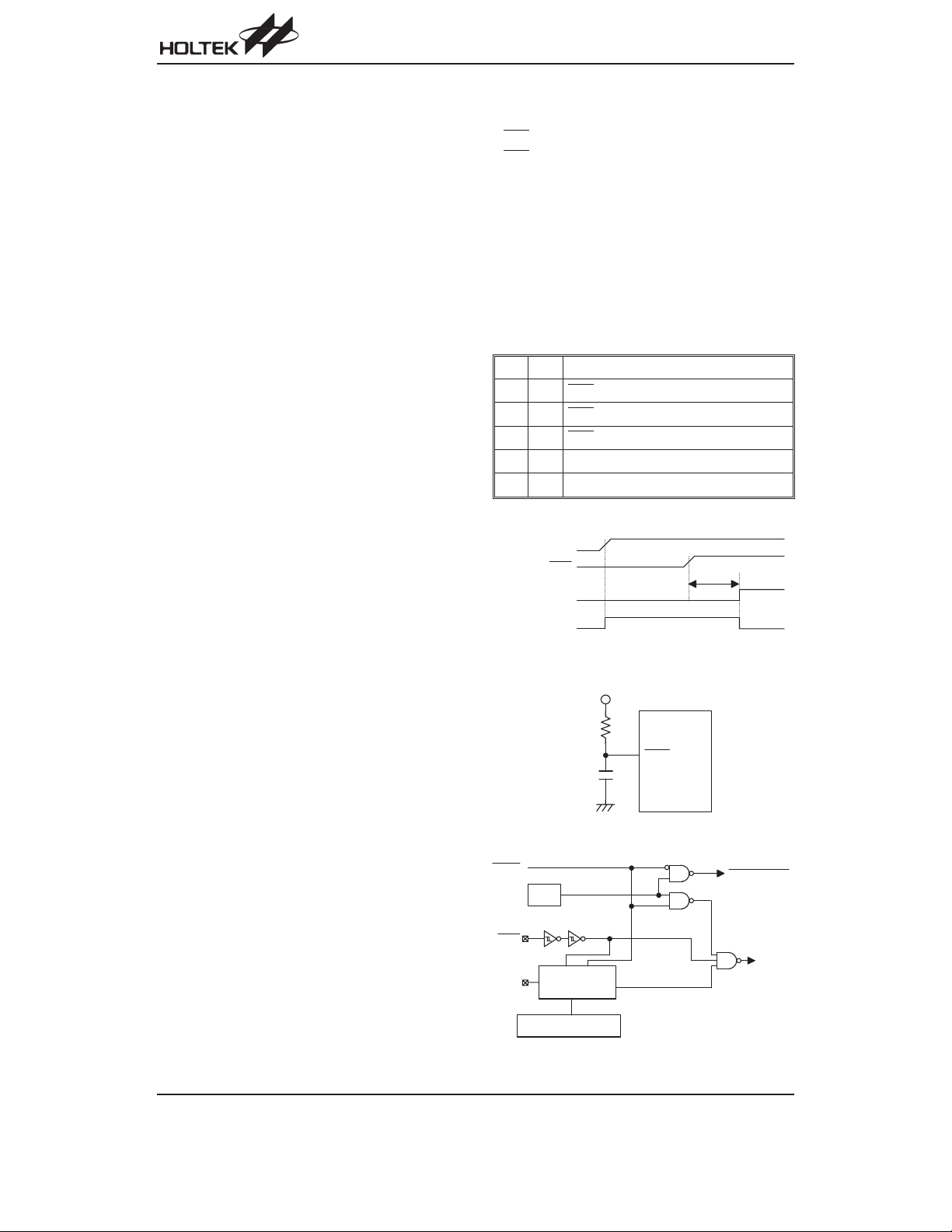
Reset
There are 3 ways in which a reset can occur:
·
RES reset during normal operation
-
·
RES reset during HALT
·
WDT time-out reset during normal operation
The WDT time-out during HALT is different from other
chip reset conditions, since it can perform a ²warm re
set² that just resets the PC and SP, leaving the other cir
cuits to maintain their state. Some registers remain un
changed during any other reset conditions. Most
registers are reset to the ²initial condition² when the re
set conditions are met. By examining the PD and TO
flags, the program can distinguish between different
²chip resets².
TO PD RESET Conditions
-
-
0 0 RES
u u RES
0 1 RES
reset during power-up
reset during normal operation
wake-up HALT
1 u WDT time-out during normal operation
-
-
1 1 WDT wake-up HALT
Note: ²u² stands for ²unchanged²
V D D
R E S
S S T T i m e - o u t
C h i p R e s e t
t
Reset timing chart
V
D D
-
-
R E S
-
-
H A L T
W D T
R E S
O S C I
1 0 - s t a g e
R i p p l e C o u n t e r
W D T
T i m e - o u t
R e s e t
S S T
Reset circuit
S S T
W a r m R e s e t
C o l d
R e s e t
-
-
-
-
P o w e r - o n D e t e c t i n g
Reset configuration
Rev. 1.00 12 June 19, 2003
Page 13
HT36A2
To guarantee that the system oscillator has started and
stabilized, the SST (System Start-up Timer) provides an
extra-delay of 1024 system clock pulses during system
power up or when the system awakes from a HALT
state.
When a system power-up occurs, the SST delay is
added during the reset period. But when the reset co
mes from the RES
wake-up from HALT will enable the SST delay.
The registers status is summarized in the following table:
Register
Program Counter 0000H 0000H 0000H 0000H 0000H
MP0 xxxx xxxx uuuu uuuu uuuu uuuu uuuu uuuu uuuu uuuu
MP1 xxxx xxxx uuuu uuuu uuuu uuuu uuuu uuuu uuuu uuuu
ACC xxxx xxxx uuuu uuuu uuuu uuuu uuuu uuuu uuuu uuuu
TBLP xxxx xxxx uuuu uuuu uuuu uuuu uuuu uuuu uuuu uuuu
TBLH xxxx xxxx uuuu uuuu uuuu uuuu uuuu uuuu uuuu uuuu
WDTS 0000 0111 0000 0111 0000 0111 0000 0111 uuuu uuuu
STATUS --00 xxxx --1u uuuu --uu uuuu --01 uuuu --11 uuuu
INTC -000 0000 -000 0000 -000 0000 -000 0000 -uuu uuuu
TMR0L xxxx xxxx uuuu uuuu uuuu uuuu uuuu uuuu uuuu uuuu
TMR0C 00-0 1000 00-0 1000 00-0 1000 00-0 1000 uu-u 1uuu
TMR1L xxxx xxxx uuuu uuuu uuuu uuuu uuuu uuuu uuuu uuuu
TMR1C 00-0 1000 00-0 1000 00-0 1000 00-0 1000 uu-u 1uuu
PA 1111 1111 1111 1111 1111 1111 1111 1111 uuuu uuuu
PAC 1111 1111 1111 1111 1111 1111 1111 1111 uuuu uuuu
PB 1111 1111 1111 1111 1111 1111 1111 1111 uuuu uuuu
PBC 1111 1111 1111 1111 1111 1111 1111 1111 uuuu uuuu
PC ---- 1111 ---- 1111 ---- 1111 ---- 1111 ---- uuuu
PCC ---- 1111 ---- 1111 ---- 1111 ---- 1111 ---- uuuu
PF ---- -000 ---- -000 ---- -000 ---- -000 ---- -uuu
CHAN 00-- -000 uu-- -uuu uu-- -uuu uu-- -uuu uu-- -uuu
FreqNH xxxx xxxx uuuu uuuu uuuu uuuu uuuu uuuu uuuu uuuu
FreqNL xxxx xxxx uuuu uuuu uuuu uuuu uuuu uuuu uuuu uuuu
AddrH ---- xxxx ---- uuuu ---- uuuu ---- uuuu ---- uuuu
AddrL xxxx xxxx uuuu uuuu uuuu uuuu uuuu uuuu uuuu uuuu
ReH ---- --xx ---- --uu ---- --uu ---- --uu ---- --uu
ReL xxxx xxxx uuuu uuuu uuuu uuuu uuuu uuuu uuuu uuuu
VolH ---- xxxx ---- uuuu ---- uuuu ---- uuuu ---- uuuu
VolL xxxx xxxx uuuu uuuu uuuu uuuu uuuu uuuu uuuu uuuu
DAC ---- --00 ---- --00 ---- --00 ---- --00 ---- --uu
pin, the SST delay is disabled. Any
Reset
(Power On)
WDT Time-out
(Normal Operation)
The functional units chip reset status are shown below.
Program counter 000H
Interrupt Disable
Prescaler Clear
WDT
-
Timer Counter (0/1) Off
Input/output ports Input mode
SP Points to the top of stack
Reset
RES
(Normal Operation)
Clear. After master reset,
WDT begins counting
RES Reset
(HALT)
WDT Time-out
(HALT)*
Note:
²*² stands for warm reset
²u² stands for unchanged
²x² stands for unknown
²-² stands for unused
Rev. 1.00 13 June 19, 2003
Page 14

HT36A2
Timer 0/1
Timer 0 is an 8-bit counter, and its clock source comes
from the system clock divided by an 8-stage prescaler.
There are two registers related to Timer 0; TMR0L(0DH)
and TMR0C(0EH). One physical registers are mapped
to TMR0L location; writing TMR0L makes the starting
value be placed in the Timer 0 preload register and
reading the TMR0 gets the contents of the Timer 0 coun
ter. The TMR0C is a control register, which defines the
division ration of the prescaler and counting enable or
disable.
Writing data to B2, B1 and B0 (bits 2, 1, 0 of TMR0C)
can yield various clock sources.
One the Timer 0 starts counting, it will count from the
current contents in the counter to FFH. Once an over
flow occurs, the counter is reloaded from a preload reg
ister, and generates an interrupt request flag (T0F; bit 2
of INTCH). To enable the counting operation, the timer
On bit (TON; bit 4 of TMR0C) should be set to ²1². For
proper operation, bit 7 of TMR0C should be set to ²1²
and bit 3, bit 6 should be set to ²0².
There are two registers related to the Timer Counter1;
TMR1L(10H), TMR1C(11H). The Timer Counter 1 oper
ates in the same manner as Timer Counter 0.
TMR0C/TMR1C
B2 B1 B0
T0F
0 0 0 SYS CLK/16
0 0 1 SYS CLK/32
0 1 0 SYS CLK/64
0 1 1 SYS CLK/128
1 0 0 SYS CLK/256
1 0 1 SYS CLK/512
1 1 0 SYS CLK/1024
1 1 1 SYS CLK/2048
TMR0C Bit 4 to enable/disable timer counting
(1=enable; 0=disable)
TMR0C Bit 3, always write ²0².
TMR0C Bit 5, always write ²0².
TMR0C Bit 6, always write ²0².
TMR0C Bit 7, always write ²1².
Input/Output Ports
There are 20 bidirectional input/output lines labeled
from PA to PC0~3, which are mapped to the data mem
ory of[12H], [14H],[16H] respectively. All these I/O ports
can be used for input and output operations. For input
operation, these ports are non-latching, that is, the in
puts must be ready at the T2 rising edge of instruction
MOV A,[m] (m=12H, 14H or 16H). For output operation,
all data is latched and remains unchanged until the out
put latch is rewritten.
Each I/O line has its own control register (PAC, PBC,
PCC0~3) to control the input/output configuration. With
this control register, CMOS output or Schmitt trigger in
put with or without pull-high resistor (mask option) struc
tures can be reconfigured dynamically under software
control. To function as an input, the corresponding latch
of the control register must write a ²1². The pull-high re
sistance will exhibit automatically if the pull-high option
is selected. The input source also depends on the con
trol register. If the control register bit is ²1², input will
read the pad state. If the control register bit is ²0², the
contents of the latches will move to the internal bus. The
latter is possible in ²read-modify-write² instruction. For
output function, CMOS is the only configuration. These
control registers are mapped to locations 13H, 15H and
17H.
After a chip reset, these input/output lines remain at high
levels or floating (mask option). Each bit of these input/output latches can be set or cleared by the SET [m].i
or CLR [m].i (m=12H, 14H or 16H) instruction.
Some instructions first input data and then follow the
output operations. For example, the SET [m].i, CLR
[m].i, CPL [m] and CPLA [m] instructions read the entire
port states into the CPU, execute the defined operations
(bit-operation), and then write the results back to the
latches or the accumulator.
Each line of port A has the capability to wake-up the de
vice.
-
-
-
-
-
-
-
-
D a t a B u s
S y s t e m
C l o c k
8 - s t a g e
P r e s c a l e r
T O N
T 0 F
T i m e r 0 / 1
P r e l o a d R e g i s t e r
T i m e r 0 / 1
R e l o a d
O v e r f l o w
Timer 0/1
Rev. 1.00 14 June 19, 2003
Page 15

HT36A2
V
D a t a B u s
W r i t e C o n t r o l R e g i s t e r
C h i p R e s e t
R e a d C o n t r o l R e g i s t e r
W r i t e I / O
R e a d I / O
S y s t e m W a k e - U p ( P A o n l y )
Q
D
Q
C K
S
Q
D
C K
Q
S
M a s k O p t i o n
V
D D
M
U
X
Input/output ports
8 Channel Wavetable Synthesizer
Memory Map Register Table (1DH~FFH)
Name Function D7 D6 D5 D4 D3 D2 D1 D0
1DH DAC high byte (no default value) DA15 DA14 DA13 DA12 DA11 DA10 DA9 DA8
1EH DAC low byte (no default value) DA7 DA6 DA5 DA4 DA3 DA2 DA1 DA0
DAON=1: DAC ON
1FH
20H Channel number selection VM FR CH2 CH1 CH0
21H High byte frequency number BL3 BL2 BL1 BL0 FR11 FR10 FR9 FR8
22H Low byte frequency number FR7 FR6 FR5 FR4 FR3 FR2 FR1 FR0
23H High byte start address ST11 ST10 ST9 ST8
24H Low byte start address ST7 ST6 ST5 ST4 ST3 ST2 ST1 ST0
25H
26H Low byte repeat number RE7 RE6 RE5 RE4 RE3 RE2 RE1 RE0
27H
28H~29H Unused
2AH Volume control VR7 VR6 VR5 VR4 VR3 VR2 VR1 VR0
2BH~2FH Unused
30H~FFH Data memory (RAM) General purpose data memory (same as 8-Bit MCU)
Note:
DAON=0: DAC OFF (default)
SELW=1: DACdata fromwavetable
SELW=0: DAC data from MCU
Wave bit select,
High byte repeat number
Envelope control,
Volume control
²¾² No function, read only, read as ²0².
Unused: No function, read only, read as ²0².
¾¾¾¾¾¾
WBS RE9 RE8
A_R ENV1 ENV0 VR9 VR8
D D
W e a k
P u l l - u p
M a s k O p t i o n
P A 0 ~ P A 7
P B 0 ~ P B 7
P C 0 ~ P C 3
DAON SELW
Rev. 1.00 15 June 19, 2003
Page 16

·
CH[2~0] channel number selection
The HT36A2 has a built-in 8 output channels and
CH[2~0] is used to define which channel is selected.
When this register is written to, the wavetable synthe
sizer will automatically output the dedicated PCM
code. So this register is also used as a start playing
key and it has to be written to after all the other
wavetable function registers are already defined.
·
Change parameter selection
These two bits, VM and FR, are used to define which
register will be updated on this selected channel.
There are two modes that can be selected to reduce
the process of setting the register. Please refer to the
statements of the following table:
VM FR Function
0 0 Update all the parameter
0 1 Only update the frequency number
1 0 Only update the volume
·
Output frequency definition
The data on BL[3~0] and FR[11~0] are used to define
the output speed of the PCM file, i.e. it can be used to
generate the tone scale. When the FR[11:0] is 800H
and BL[3:0] is 6H, each sample data of the PCM code
will be sent out sequentially.
When the f
is 6.4MHz, the formula of a tone fre-
OSC
quency is:
f
OUT=fRECORD
where f
25kHzSRFR [11~ 0]
´´
is the output signal frequency, f
OUT
(17 BL [3~0])
2
-
RECORD
SR is the frequency and sampling rate on the sample
code, respectively.
So if a voice code of C3 has been recorded which has
the f
frequency (f
of 261Hz and the SR of 11025Hz, the tone
RECORD
) of G3: f
OUT
OUT
=98Hz.
Can be obtained by using the fomula:
98Hz= 261Hz ´
25kHz
11025Hz
FR[11~ 0]
´
(17 BL [3~0])
2
-
A pair of the values FR[11~0] and BL[3~0] can be de
termined when the f
·
Start address definition
is 6.4MHz.
OSC
The HT36A2 provides two address types for extended
use, one is the program ROM address which is pro
gram counter corresponding with PF value, the other
is the start address of the PCM code.
The ST[11~0] is used to define the start address of
each PCM code and reads the waveform data from
this location. The HT36A2 provides 16 input data lines
from WA[15~0], the ST[11~0] is used to locate the ma
and
HT36A2
jor 12 bits i.e. WA[15~5] and the undefined data from
WA[4~0] is always set as 00000b. In other words, the
WA[15~0]=ST[11~0]´2
-
be located at a multiple of 32. Otherwise, the PCM
code will not be read out correctly because it has a
wrong start code.
·
Waveform format definition
The HT36A2 accepts two waveform formats to ensure
a more economical data space. WBS is used to define
the sample format of each PCM code.
1 B 2 B 3 B 4 B 5 B
8 - B i t
A s a m p l i n g d a t a c o d e ; B m e a n s o n e d a t a b y t e .
1 2 - B i t
1 H 1 M 1 L 2 L
A s a m p l i n g d a t a c o d e
N o t e : " 1 H " H i g h N i b b l e
¨
WBS=0 means the sample format is 8-bit
¨
WBS=1 means the sample format is 12-bit
The 12-bit sample format allocates location to each
sample data. Please refer to the waveform format
statement as shown below.
·
Repeat number definition
The repeat number is used to define the address
which is the repeat point of the sample. When the repeat number is defined, it will be output from the start
code to the end code once and always output the
range between the repeat address to the end code
(80H) until the volume become close.
The RE[9~0] is used to calculate the repeat address
of the PCM code. The process for setting the RE[9~0]
is to write the 2¢s complement of the repeat length to
-
RE[9~0], with the highest carry ignored. The HT36A2
will get the repeat address by adding the RE[9~0] to
the address of the end code, then jump to the address
to repeat this range.
·
-
Volume control
The HT36A2 provides the volume control independ
ently. The volume are controlled by VR[9~0] respec
tively. The chip provides 1024 levels of controllable
volume, the 000H is the maximum and 3FFH is the
minimum output volume.
-
5
. So each PCM code has to
6 B 7 B 8 B
2 H 2 M 3 H 3 M
" 1 M " M i d d l e N i b b l e
" 1 L " L o w N i b b l e
Waveform format
3 L
-
-
Rev. 1.00 16 June 19, 2003
Page 17
HT36A2
·
Envelope type definition
The HT36A2 provides a function to easily program the
envelope by setting the data of ENV[1~0] and A_R. It
forms a vibrato effect by a change of the volume to at
tach and release alternately.
The A_R signal is used to define the volume change in
attach mode or release mode and ENV[1~0] is used to
define whichvolume controlbit willbe changeable.On
the attach mode, the control bits will be sequentially
signaled down to 0. On the release mode, the control
bits will be sequentially signaled up to 1. The relation
ship is shown in the following table.
·
The PCM code definition
The HT36A2 can only solve the voice format of the
signed 8-bitraw PCM.And theMCU willtake thevoice
code 80H as the end code.
So each PCM code section must be ended with the
end code 80H.
A_R ENV1 ENV0 Volume Control Bit Control Bit Final Value Mode
0 0 0 VR2~0 111b
0 1 0 VR0 1b
x 1 1 No Bit unchanged No change mode
1 0 0 VR2~0 000b
1 1 0 VR0 0b
Mask Option
No. Mask Option Function
-
-
1 WDT source
2 CLRWDT times
3 Wake-up PA only
4 Pull-High PA, PB, PC0~3 input
5 OSC mode Crystal or Resistor type
On-chip RC/Instruction clock/
disable WDT
One time, two times
(CLR WDT1/WDT2)
Release mode0 0 1 VR1~0 11b
Attach mode1 0 1 VR1~0 00b
Envelope type definition
Rev. 1.00 17 June 19, 2003
Page 18

Application Circuit
HT36A2
V
D D
1 0
W
1 0 0 k
0 . 1mF
1 2 M H z
1 0 0 k
0 . 1mF
V D D V D D A
4 7mF
0 . 1mF
O S C 1
O S C 2
P A 0 ~ P A 7
P B 0 ~ P B 7
V
D D
P C 0 ~ P C 3
V
D D
A U D
2 0 k
W
R E S
V S S A
V S S
W
1 0
4 7mF
8
V S S
O U T N
1
7
O U T P
45
S P K
8
W
F
0 . 1
m
V r e f
F
m
2
3
I N
H T 8 2 V 7 3 3
V D D
C E
H T 3 6 A 2
V
D D
1 0
W
V D D V D D A
O S C 1
4 7mF
P A 0 ~ P A 7
0 . 1mF
P B 0 ~ P B 7
V
O S C 2
V
D D
W
R E S
P C 0 ~ P C 3
A U D
V S S A
R 1
1 k
W
D D
S P K
8
W
R 2
7 5 0
W
V S S
H T 3 6 A 2
N o t e : R 1 > R 2
Rev. 1.00 18 June 19, 2003
Page 19

Package Information
28-pin SOP (300mil) Outline Dimensions
HT36A2
2 8
A
1
C
C '
D
E
Symbol
A 394
B 290
C14
C¢
D92
E
F4
G32
H4
1 5
B
1 4
G
H
F
a
Dimensions in mil
Min. Nom. Max.
¾
¾
¾
697
¾
¾
¾
50
¾¾
¾
¾
a 0°¾10°
419
300
20
713
104
¾
38
12
Rev. 1.00 19 June 19, 2003
Page 20
48-pin SSOP (300mil) Outline Dimensions
HT36A2
4 8
A
1
C
C '
D
E
Symbol
Min. Nom. Max.
A 395
B 291
C8
C¢
613
D85
E
¾
F4
G25
H4
2 5
B
2 4
F
Dimensions in mil
¾
¾
¾
¾
¾
25
¾
¾
¾
G
a
a 0°¾8°
H
420
299
12
637
99
¾
10
35
12
Rev. 1.00 20 June 19, 2003
Page 21
Product Tape and Reel Specifications
Reel Dimensions
HT36A2
T 2
A
B
T 1
D
SOP 28W (300mil)
Symbol Description Dimensions in mm
A Reel Outer Diameter
B Reel Inner Diameter
C Spindle Hole Diameter
D Key Slit Width
T1 Space Between Flange
T2 Reel Thickness
330±1.0
62±1.5
13.0+0.5
2.0±0.5
24.8+0.3
30.2±0.2
C
-0.2
-0.2
SSOP 48W
Symbol Description Dimensions in mm
A Reel Outer Diameter
B Reel Inner Diameter
C Spindle Hole Diameter
D Key Slit Width
T1 Space Between Flange
T2 Reel Thickness
330±1.0
100±0.1
13.0+0.5
-0.2
2.0±0.5
32.2+0.3
-0.2
38.2±0.2
Rev. 1.00 21 June 19, 2003
Page 22

Carrier Tape Dimensions
HT36A2
D
E
F
PD 1
P 1P 0
W
A 0
B 0
C
SOP 28W (300mil)
Symbol Description Dimensions in mm
W Carrier Tape Width
P Cavity Pitch
E Perforation Position
F Cavity to Perforation (Width Direction)
24.0±0.3
12.0±0.1
1.75±0.1
11.5±0.1
D Perforation Diameter 1.5+0.1
D1 Cavity Hole Diameter 1.5+0.25
P0 Perforation Pitch
P1 Cavity to Perforation (Length Direction)
A0 Cavity Length
B0 Cavity Width
K0 Cavity Depth
t Carrier Tape Thickness
4.0±0.1
2.0±0.1
10.85±0.1
18.34±0.1
2.97±0.1
0.35±0.01
C Cover Tape Width 21.3
t
K 0
Rev. 1.00 22 June 19, 2003
Page 23

HT36A2
D
E
F
PD 1
P 1P 0
W
A 0
B 0
C
SSOP 48W
Symbol Description Dimensions in mm
W Carrier Tape Width
P Cavity Pitch
E Perforation Position
F Cavity to Perforation (Width Direction)
32.0±0.3
16.0±0.1
1.75±0.1
14.2±0.1
D Perforation Diameter 2.0 Min.
D1 Cavity Hole Diameter 1.5+0.25
P0 Perforation Pitch
P1 Cavity to Perforation (Length Direction)
A0 Cavity Length
B0 Cavity Width
K1 Cavity Depth
K2 Cavity Depth
t Carrier Tape Thickness
4.0±0.1
2.0±0.1
12.0±0.1
16.20±0.1
2.4±0.1
3.2±0.1
0.35±0.05
C Cover Tape Width 25.5
t
K 1
K 2
Rev. 1.00 23 June 19, 2003
Page 24

Holtek Semiconductor Inc. (Headquarters)
No.3, Creation Rd. II, Science Park, Hsinchu, Taiwan
Tel: 886-3-563-1999
Fax: 886-3-563-1189
http://www.holtek.com.tw
Holtek Semiconductor Inc. (Taipei Sales Office)
4F-2, No. 3-2, YuanQu St., Nankang Software Park, Taipei 115, Taiwan
Tel: 886-2-2655-7070
Fax: 886-2-2655-7373
Fax: 886-2-2655-7383 (International sales hotline)
HT36A2
Holtek Semiconductor Inc. (Shanghai Sales Office)
7th Floor, Building 2, No.889, Yi Shan Rd., Shanghai, China 200233
Tel: 021-6485-5560
Fax: 021-6485-0313
http://www.holtek.com.cn
Holtek Semiconductor Inc. (Shenzhen Sales Office)
5/F, Unit A, Productivity Building, Cross of Science M 3rd Road and Gaoxin M 2nd Road, Science Park, Nanshan District,
Shenzhen, China 518057
Tel: 0755-8616-9908, 8616-9308
Fax: 0755-8616-9533
Holtek Semiconductor Inc. (Beijing Sales Office)
Suite 1721, Jinyu Tower, A129 West Xuan Wu Men Street, Xicheng District, Beijing, China 100031
Tel: 010-6641-0030, 6641-7751, 6641-7752
Fax: 010-6641-0125
Holtek Semiconductor Inc. (Chengdu Sales Office)
709, Building 3, Champagne Plaza, No.97 Dongda Street, Chengdu, Sichuan, China 610016
Tel: 028-6653-6590
Fax: 028-6653-6591
Holmate Semiconductor, Inc. (North America Sales Office)
46729 Fremont Blvd., Fremont, CA 94538
Tel: 510-252-9880
Fax: 510-252-9885
http://www.holmate.com
Copyright Ó 2003 by HOLTEK SEMICONDUCTOR INC.
The information appearing in this Data Sheet is believed to be accurate at the time of publication. However, Holtek as
sumes no responsibility arising from the use of the specifications described. The applications mentioned herein are used
solely for the purpose of illustration and Holtek makes no warranty or representation that such applications will be suitable
without further modification, nor recommends the use of its products for application that may present a risk to human life
due to malfunction or otherwise. Holtek¢s products are not authorized for use as critical components in life support devices
or systems. Holtek reserves the right to alter its products without prior notification. For the most up-to-date information,
please visit our web site at http://www.holtek.com.tw.
-
Rev. 1.00 24 June 19, 2003
 Loading...