

Page 1

Holtek 32-Bit Microcontroller with Arm® Cortex®-M0+ Core
HT32F52243/HT32F52253
User Manual
Revision: V1.20 Date: September 19, 2018
Page 2

32-Bit Arm® Cortex®-M0+ MCU
HT32F52243/HT32F52253
Table of Contents
1 Introduction ........................................................................................................... 22
Overview .............................................................................................................................. 22
Features ............................................................................................................................... 23
Device Information ............................................................................................................... 27
Block Diagram ..................................................................................................................... 28
2 Document Conventions ....................................................................................... 29
3 System Architecture ............................................................................................. 30
Arm® Cortex®-M0+ Processor .............................................................................................. 30
Bus Architecture ................................................................................................................... 31
Memory Organization .......................................................................................................... 32
Memory Map ................................................................................................................................... 33
Embedded Flash Memory ............................................................................................................... 35
Embedded SRAM Memory ............................................................................................................. 35
AHB Peripherals ............................................................................................................................. 35
APB Peripherals ............................................................................................................................. 35
Table of Contents
4 Flash Memory Controller (FMC) .......................................................................... 36
Introduction .......................................................................................................................... 36
Features ............................................................................................................................... 36
Functional Descriptions ....................................................................................................... 37
Flash Memory Map ......................................................................................................................... 37
Flash Memory Architecture ............................................................................................................. 38
Wait State Setting ........................................................................................................................... 38
Booting Conguration ..................................................................................................................... 39
Page Erase ..................................................................................................................................... 40
Mass Erase ..................................................................................................................................... 41
Word Programming ......................................................................................................................... 42
Option Byte Description .................................................................................................................. 43
Page Erase/Program Protection ..................................................................................................... 44
Security Protection .......................................................................................................................... 45
Register Map ....................................................................................................................... 46
Register Descriptions ........................................................................................................... 47
Flash Target Address Register – TADR .......................................................................................... 47
Flash Write Data Register – WRDR ............................................................................................... 48
Flash Operation Command Register – OCMR ............................................................................... 49
Flash Operation Control Register – OPCR ..................................................................................... 50
Flash Operation Interrupt Enable Register – OIER ........................................................................ 51
Flash Operation Interrupt and Status Register – OISR .................................................................. 52
Flash Page Erase/Program Protection Status Register – PPSR .................................................... 53
Flash Security Protection Status Register – CPSR ........................................................................ 54
Rev. 1.20 2 of 501 September 19, 2018
Page 3

32-Bit Arm® Cortex®-M0+ MCU
HT32F52243/HT32F52253
Flash Vector Mapping Control Register – VMCR ........................................................................... 55
Flash Manufacturer and Device ID Register – MDID ...................................................................... 56
Flash Page Number Status Register – PNSR ................................................................................ 57
Flash Page Size Status Register – PSSR ...................................................................................... 58
Device ID Register – DIDR ............................................................................................................. 58
Flash Pre-fetch Control Register – CFCR ...................................................................................... 59
Custom ID Register n – CIDRn (n = 0 ~ 3) ..................................................................................... 60
5 Power Control Unit (PWRCU) .............................................................................. 61
Introduction .......................................................................................................................... 61
Features ............................................................................................................................... 62
Functional Descriptions ....................................................................................................... 62
VDD Power Domain .......................................................................................................................... 62
1.5 V Power Domain ....................................................................................................................... 64
Operation Modes ............................................................................................................................ 64
Register Map ....................................................................................................................... 66
Register Descriptions ........................................................................................................... 67
Power Control Status Register – PWRSR ...................................................................................... 67
Power Control Register – PWRCR ................................................................................................. 68
V
Power Domain Test Register – PWRTEST ............................................................................... 70
DD
Low Voltage / Brown Out Detect Control and Status Register – LVDCSR ..................................... 70
Table of Contents
6 Clock Control Unit (CKCU) .................................................................................. 72
Introduction .......................................................................................................................... 72
Features ............................................................................................................................... 72
Function Descriptions .......................................................................................................... 74
High Speed External Crystal Oscillator – HSE ............................................................................... 74
High Speed Internal RC Oscillator – HSI ........................................................................................ 75
Auto Trimming of High Speed Internal RC Oscillator – HSI ............................................................ 75
Phase Locked Loop – PLL .............................................................................................................. 76
Low Speed External Crystal Oscillator – LSE ................................................................................. 78
Low Speed Internal RC Oscillator – LSI ......................................................................................... 78
Clock Ready Flag ........................................................................................................................... 78
System Clock (CK_SYS) Selection ................................................................................................ 79
HSE Clock Monitor ......................................................................................................................... 80
Clock Output Capability .................................................................................................................. 80
Register Map ....................................................................................................................... 81
Register Descriptions ........................................................................................................... 82
Global Clock Conguration Register – GCFGR .............................................................................. 82
Global Clock Control Register – GCCR .......................................................................................... 83
Global Clock Status Register – GCSR ........................................................................................... 84
Global Clock Interrupt Register – GCIR .......................................................................................... 85
PLL Conguration Register – PLLCFGR ........................................................................................ 86
PLL Control Register – PLLCR ....................................................................................................... 86
Rev. 1.20 3 of 501 September 19, 2018
Page 4

32-Bit Arm® Cortex®-M0+ MCU
HT32F52243/HT32F52253
AHB Conguration Register – AHBCFGR ...................................................................................... 87
AHB Clock Control Register – AHBCCR ........................................................................................ 88
APB Conguration Register – APBCFGR ....................................................................................... 90
APB Clock Control Register 0 – APBCCR0 .................................................................................... 91
APB Clock Control Register 1 – APBCCR1 .................................................................................... 92
Clock Source Status Register – CKST ........................................................................................... 94
APB Peripheral Clock Selection Register 0 – APBPCSR0 ............................................................. 95
APB Peripheral Clock Selection Register 1 – APBPCSR1 ............................................................. 97
HSI Control Register – HSICR ........................................................................................................ 99
HSI Auto Trimming Counter Register – HSIATCR ........................................................................ 100
MCU Debug Control Register – MCUDBGCR .............................................................................. 101
7 Reset Control Unit (RSTCU) .............................................................................. 104
Introduction ........................................................................................................................ 104
Functional Descriptions ..................................................................................................... 105
Power On Reset ........................................................................................................................... 105
System Reset ............................................................................................................................... 105
AHB and APB Unit Reset .............................................................................................................. 105
Register Map ..................................................................................................................... 106
Register Descriptions ......................................................................................................... 107
Global Reset Status Register – GRSR ......................................................................................... 107
AHB Peripheral Reset Register – AHBPRSTR ............................................................................. 108
APB Peripheral Reset Register 0 – APBPRSTR0 ........................................................................ 109
APB Peripheral Reset Register 1 – APBPRSTR1 .........................................................................110
Table of Contents
8 General Purpose I/O (GPIO) ............................................................................... 112
Introduction ........................................................................................................................ 112
Features ............................................................................................................................. 113
Functional Descriptions ..................................................................................................... 113
Default GPIO Pin Conguration .....................................................................................................113
General Purpose I/O – GPIO .........................................................................................................113
GPIO Locking Mechanism .............................................................................................................115
Register Map ..................................................................................................................... 115
Register Descriptions ......................................................................................................... 116
Port A Data Direction Control Register – PADIRCR ......................................................................116
Port A Input Function Enable Control Register – PAINER .............................................................117
Port A Pull-Up Selection Register – PAPUR ..................................................................................118
Port A Pull-Down Selection Register – PAPDR .............................................................................119
Port A Open Drain Selection Register – PAODR .......................................................................... 120
Port A Output Current Drive Selection Register – PADRVR ......................................................... 121
Port A Lock Register – PALOCKR ................................................................................................ 122
Port A Data Input Register – PADINR ........................................................................................... 123
Port A Output Data Register – PADOUTR .................................................................................... 123
Port A Output Set/Reset Control Register – PASRR .................................................................... 124
Rev. 1.20 4 of 501 September 19, 2018
Page 5

32-Bit Arm® Cortex®-M0+ MCU
HT32F52243/HT32F52253
Port A Output Reset Register – PARR .......................................................................................... 125
Port B Data Direction Control Register – PBDIRCR ..................................................................... 125
Port B Input Function Enable Control Register – PBINER ........................................................... 126
Port B Pull-Up Selection Register – PBPUR ................................................................................ 127
Port B Pull-Down Selection Register – PBPDR ............................................................................ 128
Port B Open Drain Selection Register – PBODR ......................................................................... 129
Port B Output Current Drive Selection Register – PBDRVR ........................................................ 130
Port B Lock Register – PBLOCKR ................................................................................................ 131
Port B Data Input Register – PBDINR .......................................................................................... 132
Port B Output Data Register – PBDOUTR ................................................................................... 132
Port B Output Set/Reset Control Register – PBSRR .................................................................... 133
Port B Output Reset Register – PBRR ......................................................................................... 134
Port C Data Direction Control Register – PCDIRCR .................................................................... 134
Port C Input Function Enable Control Register – PCINER ........................................................... 135
Port C Pull-Up Selection Register – PCPUR ................................................................................ 136
Port C Pull-Down Selection Register – PCPDR ........................................................................... 137
Port C Open Drain Selection Register – PCODR ......................................................................... 138
Port C Output Current Drive Selection Register – PCDRVR ........................................................ 139
Port C Lock Register – PCLOCKR ............................................................................................... 140
Port C Data Input Register – PCDINR .......................................................................................... 141
Port C Output Data Register – PCDOUTR ................................................................................... 141
Port C Output Set/Reset Control Register – PCSRR ................................................................... 142
Port C Output Reset Register – PCRR ......................................................................................... 143
Port D Data Direction Control Register – PDDIRCR .................................................................... 143
Port D Input Function Enable Control Register – PDINER ........................................................... 144
Port D Pull-Up Selection Register – PDPUR ................................................................................ 145
Port D Pull-Down Selection Register – PDPDR ........................................................................... 146
Port D Open Drain Selection Register – PDODR ......................................................................... 147
Port D Output Current Drive Selection Register – PDDRVR ........................................................ 148
Port D Lock Register – PDLOCKR ............................................................................................... 149
Port D Data Input Register – PDDINR .......................................................................................... 150
Port D Output Data Register – PDDOUTR ................................................................................... 150
Port D Output Set/Reset Control Register – PDSRR ................................................................... 151
Port D Output Reset Register – PDRR ......................................................................................... 152
Table of Contents
9 Alternate Function Input/Output Control Unit (AFIO) ...................................... 153
Introduction ........................................................................................................................ 153
Features ............................................................................................................................. 154
Functional Descriptions ..................................................................................................... 154
External Interrupt Pin Selection .................................................................................................... 154
Alternate Function ......................................................................................................................... 155
Lock Mechanism .......................................................................................................................... 155
Register Map ..................................................................................................................... 155
Register Descriptions ......................................................................................................... 156
EXTI Source Selection Register 0 – ESSR0 ................................................................................ 156
Rev. 1.20 5 of 501 September 19, 2018
Page 6

32-Bit Arm® Cortex®-M0+ MCU
HT32F52243/HT32F52253
EXTI Source Selection Register 1 – ESSR1 ................................................................................ 157
GPIO Port x Conguration Low Register – GPxCFGLR, x = A, B, C, D ....................................... 158
GPIO Port x Conguration High Register – GPxCFGHR, x = A, B, C, D ...................................... 159
10 Nested Vectored Interrupt Controller (NVIC) .................................................. 160
Introduction ........................................................................................................................ 160
Features ............................................................................................................................. 161
Function Descriptions ........................................................................................................ 162
SysTick Calibration ....................................................................................................................... 162
Register Map ..................................................................................................................... 162
11 External Interrupt / Event Controller (EXTI) .................................................... 163
Introduction ........................................................................................................................ 163
Features ............................................................................................................................. 163
Function Descriptions ........................................................................................................ 164
Wakeup Event Management......................................................................................................... 164
External Interrupt/Event Line Mapping ......................................................................................... 165
Interrupt and Debounce ................................................................................................................ 165
Register Map .................................................................................................................... 166
Register Descriptions ......................................................................................................... 167
EXTI Interrupt Conguration Register n – EXTICFGRn, n = 0 ~ 15 ............................................. 167
EXTI Interrupt Control Register – EXTICR ................................................................................... 168
EXTI Interrupt Edge Flag Register – EXTIEDGEFLGR ................................................................ 169
EXTI Interrupt Edge Status Register – EXTIEDGESR ................................................................. 170
EXTI Interrupt Software Set Command Register – EXTISSCR .................................................... 170
EXTI Interrupt Wakeup Control Register – EXTIWAKUPCR ........................................................ 171
EXTI Interrupt Wakeup Polarity Register – EXTIWAKUPPOLR ................................................... 172
EXTI Interrupt Wakeup Flag Register – EXTIWAKUPFLG ........................................................... 172
Table of Contents
12 Analog to Digital Converter (ADC) .................................................................. 173
Introduction ........................................................................................................................ 173
Features ............................................................................................................................. 174
Function Descriptions ........................................................................................................ 175
ADC Clock Setup .......................................................................................................................... 175
Channel Selection ......................................................................................................................... 175
Conversion Mode .......................................................................................................................... 175
Start Conversion on External Event .............................................................................................. 178
Sampling Time Setting .................................................................................................................. 179
Data Format .................................................................................................................................. 179
Analog Watchdog.......................................................................................................................... 179
Interrupts ....................................................................................................................................... 180
Register Map ..................................................................................................................... 181
Register Descriptions ......................................................................................................... 182
ADC Conversion Control Register – ADCCR ............................................................................... 182
Rev. 1.20 6 of 501 September 19, 2018
Page 7

32-Bit Arm® Cortex®-M0+ MCU
HT32F52243/HT32F52253
ADC Conversion List Register 0 – ADCLST0 ............................................................................... 183
ADC Conversion List Register 1 – ADCLST1 ............................................................................... 184
ADC Input Sampling Time Register – ADCSTR ........................................................................... 185
ADC Conversion Data Register y – ADCDRy, y = 0 ~ 7 ............................................................... 186
ADC Trigger Control Register – ADCTCR .................................................................................... 187
ADC Trigger Source Register – ADCTSR ..................................................................................... 188
ADC Watchdog Control Register – ADCWCR .............................................................................. 189
ADC Watchdog Threshold Register – ADCTR .............................................................................. 190
ADC Interrupt Enable Register – ADCIER ................................................................................... 191
ADC Interrupt Raw Status Register – ADCIRAW ......................................................................... 192
ADC Interrupt Status Register – ADCISR ..................................................................................... 193
ADC Interrupt Clear Register – ADCICLR .................................................................................... 194
13 General-Purpose Timer (GPTM) ...................................................................... 195
Introduction ........................................................................................................................ 195
Features ............................................................................................................................. 196
Functional Descriptions ..................................................................................................... 196
Counter Mode ............................................................................................................................... 196
Clock Controller ............................................................................................................................ 198
Trigger Controller .......................................................................................................................... 199
Slave Controller ............................................................................................................................ 201
Master Controller .......................................................................................................................... 203
Channel Controller ........................................................................................................................ 203
Input Stage ................................................................................................................................... 206
Quadrature Decoder ..................................................................................................................... 207
Output Stage ................................................................................................................................. 209
Update Management .................................................................................................................... 213
Single Pulse Mode ........................................................................................................................ 213
Asymmetric PWM Mode ............................................................................................................... 215
Timer Interconnection ................................................................................................................... 216
Trigger ADC Start.......................................................................................................................... 219
PDMA Request ............................................................................................................................. 219
Register Map ..................................................................................................................... 220
Register Descriptions ......................................................................................................... 221
Timer Counter Conguration Register – CNTCFR ....................................................................... 221
Timer Mode Conguration Register – MDCFR ............................................................................. 222
Timer Trigger Conguration Register – TRCFR ............................................................................ 225
Timer Control Register – CTR ...................................................................................................... 226
Channel 0 Input Conguration Register – CH0ICFR .................................................................... 227
Channel 1 Input Conguration Register – CH1ICFR .................................................................... 229
Channel 2 Input Conguration Register – CH2ICFR .................................................................... 231
Channel 3 Input Conguration Register – CH3ICFR .................................................................... 233
Channel 0 Output Conguration Register – CH0OCFR ............................................................... 235
Channel 1 Output Conguration Register – CH1OCFR ............................................................... 237
Table of Contents
Rev. 1.20 7 of 501 September 19, 2018
Page 8

32-Bit Arm® Cortex®-M0+ MCU
HT32F52243/HT32F52253
Channel 2 Output Conguration Register – CH2OCFR ............................................................... 239
Channel 3 Output Conguration Register – CH3OCFR ............................................................... 241
Channel Control Register – CHCTR ............................................................................................. 243
Channel Polarity Conguration Register – CHPOLR .................................................................... 244
Timer PDMA/Interrupt Control Register – DICTR ......................................................................... 245
Timer Event Generator Register – EVGR ..................................................................................... 246
Timer Interrupt Status Register – INTSR ...................................................................................... 248
Timer Counter Register – CNTR................................................................................................... 250
Timer Prescaler Register – PSCR ................................................................................................ 250
Timer Counter Reload Register – CRR ........................................................................................ 251
Channel 0 Capture/Compare Register – CH0CCR ...................................................................... 251
Channel 1 Capture/Compare Register – CH1CCR ...................................................................... 252
Channel 2 Capture/Compare Register – CH2CCR ...................................................................... 253
Channel 3 Capture/Compare Register – CH3CCR ...................................................................... 254
Channel 0 Asymmetric Compare Register – CH0ACR ................................................................. 255
Channel 1 Asymmetric Compare Register – CH1ACR ................................................................. 255
Channel 2 Asymmetric Compare Register – CH2ACR ................................................................. 256
Channel 3 Asymmetric Compare Register – CH3ACR ................................................................. 256
Table of Contents
14 Basic Function Timer (BFTM) .......................................................................... 257
Introduction ........................................................................................................................ 257
Features ............................................................................................................................. 257
Functional Description ....................................................................................................... 258
Repetitive Mode ............................................................................................................................ 258
One Shot Mode ............................................................................................................................. 259
Trigger ADC Start.......................................................................................................................... 260
Register Map ..................................................................................................................... 260
Register Descriptions ......................................................................................................... 261
BFTM Control Register – BFTMCR .............................................................................................. 261
BFTM Status Register – BFTMSR ................................................................................................ 262
BFTM Counter Register – BFTMCNTR ........................................................................................ 263
BFTM Compare Value Register – BFTMCMPR ........................................................................... 263
15 Motor Control Timer (MCTM) ........................................................................... 264
Introduction ........................................................................................................................ 264
Features ............................................................................................................................. 265
Functional Descriptions ..................................................................................................... 266
Counter Mode ............................................................................................................................... 266
Clock Controller ............................................................................................................................ 269
Trigger Controller .......................................................................................................................... 269
Slave Controller ............................................................................................................................ 271
Master Controller .......................................................................................................................... 273
Channel Controller ........................................................................................................................ 274
Input Stage ................................................................................................................................... 275
Rev. 1.20 8 of 501 September 19, 2018
Page 9

32-Bit Arm® Cortex®-M0+ MCU
HT32F52243/HT32F52253
Output Stage ................................................................................................................................. 277
Update Management .................................................................................................................... 287
Single Pulse Mode ........................................................................................................................ 289
Asymmetric PWM Mode ............................................................................................................... 291
Timer Interconnection ................................................................................................................... 292
Trigger ADC Start.......................................................................................................................... 296
Lock Level Table ........................................................................................................................... 296
PDMA Request ............................................................................................................................. 297
Register Map ..................................................................................................................... 298
Register Descriptions ......................................................................................................... 299
Timer Counter Conguration Register – CNTCFR ....................................................................... 299
Timer Mode Conguration Register – MDCFR ............................................................................. 300
Timer Trigger Conguration Register – TRCFR ............................................................................ 303
Timer Control Register – CTR ...................................................................................................... 304
Channel 0 Input Conguration Register – CH0ICFR .................................................................... 305
Channel 1 Input Conguration Register – CH1ICFR .................................................................... 307
Channel 2 Input Conguration Register – CH2ICFR .................................................................... 309
Channel 3 Input Conguration Register – CH3ICFR .....................................................................311
Channel 0 Output Conguration Register – CH0OCFR ............................................................... 313
Channel 1 Output Conguration Register – CH1OCFR ............................................................... 315
Channel 2 Output Conguration Register – CH2OCFR ............................................................... 317
Channel 3 Output Conguration Register – CH3OCFR ............................................................... 319
Channel Control Register – CHCTR ............................................................................................. 321
Channel Polarity Conguration Register – CHPOLR .................................................................... 323
Channel Break Conguration Register – CHBRKCFR ................................................................. 324
Channel Break Control Register – CHBRKCTR ........................................................................... 325
Timer PDMA/Interrupt Control Register – DICTR ......................................................................... 327
Timer Event Generator Register – EVGR ..................................................................................... 329
Timer Interrupt Status Register – INTSR ...................................................................................... 331
Timer Counter Register – CNTR................................................................................................... 333
Timer Prescaler Register – PSCR ................................................................................................ 334
Timer Counter Reload Register – CRR ........................................................................................ 335
Timer Repetition Register – REPR ............................................................................................... 335
Channel 0 Capture/Compare Register – CH0CCR ...................................................................... 336
Channel 1 Capture/Compare Register – CH1CCR ...................................................................... 337
Channel 2 Capture/Compare Register – CH2CCR ...................................................................... 338
Channel 3 Capture/Compare Register – CH3CCR ...................................................................... 339
Channel 0 Asymmetric Compare Register – CH0ACR ................................................................. 340
Channel 1 Asymmetric Compare Register – CH1ACR ................................................................. 340
Channel 2 Asymmetric Compare Register – CH2ACR ................................................................. 341
Channel 3 Asymmetric Compare Register – CH3ACR ................................................................. 341
Table of Contents
Rev. 1.20 9 of 501 September 19, 2018
Page 10

32-Bit Arm® Cortex®-M0+ MCU
HT32F52243/HT32F52253
16 Single-Channel Timer (SCTM) ......................................................................... 342
Introduction ........................................................................................................................ 342
Features ............................................................................................................................. 342
Functional Descriptions ..................................................................................................... 343
Counter Mode ............................................................................................................................... 343
Clock Controller ............................................................................................................................ 343
Trigger Controller .......................................................................................................................... 344
Slave Controller ............................................................................................................................ 346
Channel Controller ........................................................................................................................ 348
Input Stage ................................................................................................................................... 349
Output Stage ................................................................................................................................. 350
Update Management .................................................................................................................... 353
Register Map ..................................................................................................................... 354
Register Descriptions ......................................................................................................... 355
Timer Counter Conguration Register – CNTCFR ....................................................................... 355
Timer Mode Conguration Register – MDCFR ............................................................................. 356
Timer Trigger Conguration Register – TRCFR ............................................................................ 357
Timer Control Register – CTR ...................................................................................................... 358
Channel Input Conguration Register – CHICFR ......................................................................... 359
Channel Output Conguration Register – CHOCFR .................................................................... 361
Channel Control Register – CHCTR ............................................................................................. 362
Channel Polarity Conguration Register – CHPOLR .................................................................... 363
Timer Interrupt Control Register – DICTR .................................................................................... 364
Timer Event Generator Register – EVGR ..................................................................................... 365
Timer Interrupt Status Register – INTSR ...................................................................................... 366
Timer Counter Register – CNTR................................................................................................... 367
Timer Prescaler Register – PSCR ................................................................................................ 367
Timer Counter Reload Register – CRR ........................................................................................ 368
Channel Capture/Compare Register – CHCCR ........................................................................... 369
Table of Contents
17 Real Time Clock (RTC) ..................................................................................... 370
Introduction ........................................................................................................................ 370
Features ............................................................................................................................. 370
Functional Descriptions ..................................................................................................... 371
RTC Related Register Reset ........................................................................................................ 371
Reading RTC Register .................................................................................................................. 371
Low Speed Clock Conguration ................................................................................................... 371
RTC Counter Operation ................................................................................................................ 372
Interrupt and Wakeup Control ....................................................................................................... 372
RTCOUT Output Pin Conguration............................................................................................... 373
Register Map ..................................................................................................................... 374
Register Descriptions ......................................................................................................... 374
RTC Counter Register – RTCCNT ................................................................................................ 374
RTC Compare Register – RTCCMP ............................................................................................. 375
Rev. 1.20 10 of 501 September 19, 2018
Page 11

32-Bit Arm® Cortex®-M0+ MCU
HT32F52243/HT32F52253
RTC Control Register – RTCCR ................................................................................................... 376
RTC Status Register – RTCSR..................................................................................................... 378
RTC Interrupt and Wakeup Enable Register – RTCIWEN ............................................................ 379
18 Watchdog Timer (WDT) .................................................................................... 380
Introduction ........................................................................................................................ 380
Features ............................................................................................................................. 380
Functional Description ....................................................................................................... 381
Register Map ..................................................................................................................... 382
Register Descriptions ......................................................................................................... 383
Watchdog Timer Control Register – WDTCR ............................................................................... 383
Watchdog Timer Mode Register 0 – WDTMR0............................................................................. 384
Watchdog Timer Mode Register 1 – WDTMR1............................................................................. 385
Watchdog Timer Status Register – WDTSR ................................................................................. 386
Watchdog Timer Protection Register – WDTPR ........................................................................... 387
Watchdog Timer Clock Selection Register – WDTCSR ................................................................ 388
Table of Contents
19 Inter-Integrated Circuit – I2C ............................................................................ 389
Introduction ........................................................................................................................ 389
Features ............................................................................................................................. 390
Functional Descriptions ..................................................................................................... 390
Two Wire Serial Interface .............................................................................................................. 390
START and STOP Conditions ....................................................................................................... 390
Data Validity .................................................................................................................................. 391
Addressing Format ....................................................................................................................... 392
Data Transfer and Acknowledge ................................................................................................... 393
Clock Synchronization .................................................................................................................. 394
Arbitration ..................................................................................................................................... 395
General Call Address .................................................................................................................... 395
Bus Error ....................................................................................................................................... 395
Address Mask Enable ................................................................................................................... 396
Address Snoop ............................................................................................................................. 396
Operation Mode ............................................................................................................................ 396
Master Transmitter Mode .............................................................................................................. 396
Master Receiver Mode .................................................................................................................. 397
Slave Transmitter Mode ................................................................................................................ 399
Slave Receiver Mode .................................................................................................................... 400
Conditions of Holding SCL Line .................................................................................................... 401
I2C Timeout Function .................................................................................................................... 402
PDMA Interface ............................................................................................................................. 402
Register Map ..................................................................................................................... 403
Register Descriptions ......................................................................................................... 404
I2C Control Register – I2CCR ....................................................................................................... 404
I2C Interrupt Enable Register – I2CIER ........................................................................................ 406
Rev. 1.20 11 of 501 September 19, 2018
Page 12

32-Bit Arm® Cortex®-M0+ MCU
HT32F52243/HT32F52253
I2C Address Register – I2CADDR ................................................................................................. 407
I2C Status Register – I2CSR ......................................................................................................... 408
I2C SCL High Period Generation Register – I2CSHPGR ...............................................................411
I2C SCL Low Period Generation Register – I2CSLPGR ............................................................... 412
I2C Data Register – I2CDR ........................................................................................................... 413
I2C Target Register – I2CTAR ....................................................................................................... 414
I2C Address Mask Register – I2CADDMR .................................................................................... 415
I2C Address Snoop Register – I2CADDSR ................................................................................... 416
I2C Timeout Register – I2CTOUT.................................................................................................. 417
20 Serial Peripheral Interface (SPI) ...................................................................... 418
Introduction ........................................................................................................................ 418
Features ............................................................................................................................. 419
Function Descriptions ........................................................................................................ 419
Master Mode ................................................................................................................................. 419
Slave Mode ................................................................................................................................... 419
SPI Serial Frame Format .............................................................................................................. 420
Status Flags .................................................................................................................................. 424
PDMA Interface ............................................................................................................................. 427
Register Map ..................................................................................................................... 427
Register Descriptions ......................................................................................................... 428
SPI Control Register 0 – SPICR0 ................................................................................................. 428
SPI Control Register 1 – SPICR1 ................................................................................................. 430
SPI Interrupt Enable Register – SPIIER ....................................................................................... 432
SPI Clock Prescaler Register – SPICPR ...................................................................................... 433
SPI Data Register – SPIDR .......................................................................................................... 434
SPI Status Register – SPISR ........................................................................................................ 435
SPI FIFO Control Register – SPIFCR ........................................................................................... 436
SPI FIFO Status Register – SPIFSR ............................................................................................ 437
SPI FIFO Time Out Counter Register – SPIFTOCR ..................................................................... 438
Table of Contents
21 Universal Synchronous Asynchronous Receiver Transmitter (USART) .... 439
Introduction ........................................................................................................................ 439
Features ............................................................................................................................ 440
Function Descriptions ........................................................................................................ 441
Serial Data Format ........................................................................................................................ 441
Baud Rate Generation .................................................................................................................. 442
Hardware Flow Control ................................................................................................................. 443
IrDA ............................................................................................................................................... 445
RS485 Mode ................................................................................................................................. 447
Synchronous Master Mode ........................................................................................................... 449
Interrupts and Status .................................................................................................................... 451
PDMA Interface ............................................................................................................................. 451
Register Map ..................................................................................................................... 452
Rev. 1.20 12 of 501 September 19, 2018
Page 13

32-Bit Arm® Cortex®-M0+ MCU
HT32F52243/HT32F52253
Register Descriptions ......................................................................................................... 453
USART Data Register – USRDR .................................................................................................. 453
USART Control Register – USRCR .............................................................................................. 454
USART FIFO Control Register – USRFCR................................................................................... 456
USART Interrupt Enable Register – USRIER ............................................................................... 457
USART Status & Interrupt Flag Register – USRSIFR................................................................... 458
USART Timing Parameter Register – USRTPR ........................................................................... 460
USART IrDA Control Register – IrDACR ..................................................................................... 461
USART RS485 Control Register – RS485CR............................................................................... 462
USART Synchronous Control Register – SYNCR ........................................................................ 463
USART Divider Latch Register – USRDLR.................................................................................. 464
USART Test Register – USRTSTR .............................................................................................. 465
22 Universal Asynchronous Receiver Transmitter (UART) ............................... 466
Introduction ........................................................................................................................ 466
Features ............................................................................................................................ 467
Function Descriptions ........................................................................................................ 467
Serial Data Format ........................................................................................................................ 467
Baud Rate Generation .................................................................................................................. 468
Interrupts and Status .................................................................................................................... 469
PDMA Interface ............................................................................................................................. 469
Register Map ..................................................................................................................... 470
Register Descriptions ......................................................................................................... 470
UART Data Register – URDR ....................................................................................................... 470
UART Control Register – URCR ................................................................................................... 471
UART Interrupt Enable Register – URIER .................................................................................... 473
UART Status & Interrupt Flag Register – URSIFR ....................................................................... 474
UART Divider Latch Register – URDLR ....................................................................................... 475
UART Test Register – URTSTR ................................................................................................... 476
Table of Contents
23 Peripheral Direct Memory Access (PDMA) ..................................................... 477
Introduction ........................................................................................................................ 477
Features ............................................................................................................................. 477
Functional Description ....................................................................................................... 478
AHB Master .................................................................................................................................. 478
PDMA Channel ............................................................................................................................. 478
PDMA Request Mapping .............................................................................................................. 478
Channel transfer ........................................................................................................................... 479
Channel Priority ............................................................................................................................ 479
Transfer Request .......................................................................................................................... 480
Address Mode ............................................................................................................................... 480
Auto-Reload .................................................................................................................................. 481
Transfer Interrupt .......................................................................................................................... 481
Register Map ..................................................................................................................... 482
Rev. 1.20 13 of 501 September 19, 2018
Page 14

32-Bit Arm® Cortex®-M0+ MCU
HT32F52243/HT32F52253
Register Descriptions ......................................................................................................... 483
PDMA Channel n Control Register – PDMACHnCR, n = 0 ~ 5 .................................................... 483
PDMA Channel n Source Address Register – PDMACHnSADR, n = 0 ~ 5 .................................. 485
PDMA Channel n Destination Address Register – PDMACHnDADR, n = 0 ~ 5 ........................... 485
PDMA Channel n Transfer Size Register – PDMACHnTSR, n = 0 ~ 5 ........................................ 486
PDMA Channel n Current Transfer Size Register – PDMACHnCTSR, n = 0 ~ 5 ......................... 487
PDMA Interrupt Status Register – PDMAISR ............................................................................... 487
PDMA Interrupt Status Clear Register – PDMAISCR ................................................................... 489
PDMA Interrupt Enable Register – PDMAIER .............................................................................. 490
24 Cyclic Redundancy Check (CRC) .................................................................... 491
Introduction ....................................................................................................................... 491
Features ............................................................................................................................. 491
Function Descriptions ........................................................................................................ 492
CRC Computation ......................................................................................................................... 492
Byte and Bit Reversal for CRC Computation ................................................................................ 492
CRC with PDMA ........................................................................................................................... 493
Register Map ..................................................................................................................... 493
Register Descriptions ......................................................................................................... 494
CRC Control Register – CRCCR .................................................................................................. 494
CRC Seed Register – CRCSDR ................................................................................................... 495
CRC Checksum Register – CRCCSR .......................................................................................... 495
CRC Data Register – CRCDR ...................................................................................................... 496
Table of Contents
25 Divider (DIV) ...................................................................................................... 497
Introduction ........................................................................................................................ 497
Features ............................................................................................................................. 497
Functional Descriptions ..................................................................................................... 497
Register Map ..................................................................................................................... 498
Register Descriptions ......................................................................................................... 498
Divider Control Register – CR ...................................................................................................... 498
Dividend Data Register – DDR ..................................................................................................... 499
Divisor Data Register – DSR ........................................................................................................ 499
Quotient Data Register – QTR ...................................................................................................... 500
Remainder Data Register – RMR ................................................................................................. 500
Rev. 1.20 14 of 501 September 19, 2018
Page 15

32-Bit Arm® Cortex®-M0+ MCU
HT32F52243/HT32F52253
List of Tables
Table 1. Features and Peripheral List ..................................................................................................... 27
Table 2. Document Conventions ............................................................................................................. 29
Table 3. Register Map ............................................................................................................................. 34
Table 4. Flash Memory and Option Byte ................................................................................................. 38
Table 5. Relationship between wait state cycle and HCLK ..................................................................... 38
Table 6. Booting Modes .......................................................................................................................... 39
Table 7. Option Byte Memory Map ......................................................................................................... 43
Table 8. Access Permission of Protected Main Flash Page .................................................................... 44
Table 9. Access Permission When Security Protection is Enabled ......................................................... 45
Table 10. FMC Register Map .................................................................................................................. 46
Table 11. Operation Mode Denitions ..................................................................................................... 64
Table 12. Enter/Exit Power Saving Modes .............................................................................................. 65
Table 13. Power Status After System Reset ........................................................................................... 66
Table 14. PWRCU Register Map ............................................................................................................ 66
Table 15. Output Divider2 Value Mapping............................................................................................... 77
Table 16. Feedback Divider2 Value Mapping.......................................................................................... 77
Table 17. CKOUT Clock Source ............................................................................................................. 80
Table 18. CKCU Register Map ............................................................................................................... 81
Table 19. RSTCU Register Map ........................................................................................................... 106
Table 20. AFIO, GPIO and IO Pad Control Signal True Table................................................................11 4
Table 21. GPIO Register Map ................................................................................................................115
Table 22. AFIO Selection for Peripheral Map Example ......................................................................... 155
Table 23. AFIO Register Map ................................................................................................................ 155
Table 24. Exception Types .................................................................................................................... 160
Table 25. NVIC Register Map ............................................................................................................... 162
Table 26. EXTI Register Map ................................................................................................................ 166
Table 27. Data format in ADCDR [15:0] ................................................................................................ 179
Table 28. A/D Converter Register Map ................................................................................................. 181
Table 29. Counting Direction and Encoding Signals ............................................................................. 208
Table 30. Compare Match Output Setup .............................................................................................. 210
Table 31. GPTM Register Map ............................................................................................................. 220
Table 32. GPTM Internal Trigger Connection ....................................................................................... 225
Table 33. BFTM Register Map .............................................................................................................. 260
Table 34. Compare Match Output Setup .............................................................................................. 278
Table 35. Output Control Bits for Complementary Output with a Break Event Occurrence .................. 286
Table 36. Lock Level Table.................................................................................................................... 296
Table 37. MCTM Register Map ............................................................................................................. 298
Table 38. MCTM Internal Trigger Connection ....................................................................................... 303
Table 39. Compare Match Output Setup .............................................................................................. 351
List of Tables
Rev. 1.20 15 of 501 September 19, 2018
Page 16

32-Bit Arm® Cortex®-M0+ MCU
HT32F52243/HT32F52253
Table 40. SCTM Register Map .............................................................................................................. 354
Table 41. LSE Startup Mode Operating Current and Startup Time ....................................................... 371
Table 42. RTCOUT Output Mode and Active Level Setting .................................................................. 373
Table 43. RTC Register Map................................................................................................................. 374
Table 44. Watchdog Timer Register Map .............................................................................................. 382
Table 45. Conditions of Holding SCL line .............................................................................................. 401
Table 46. I2C Register Map ................................................................................................................... 403
Table 47. I2C Clock Setting Example .................................................................................................... 412
Table 48. SPI Interface Format Setup ................................................................................................... 420
Table 49. SPI Mode Fault Trigger Conditions ....................................................................................... 425
Table 50. SPI Master Mode SEL Pin Status. ........................................................................................ 426
Table 51. SPI Register Map .................................................................................................................. 427
Table 52. Baud Rate Deviation Error Calculation – CK_USART = 40 MHz. ......................................... 442
Table 53. Baud Rate Deviation Error Calculation – CK_USART = 48 MHz. ......................................... 443
Table 54. USART Register Map ............................................................................................................ 452
Table 55. Baud Rate Deviation Error Calculation – CK_UART = 40 MHz. ........................................... 468
Table 56. Baud Rate Deviation Error Calculation – CK_UART = 48 MHz. ........................................... 469
Table 57. UART Register Map .............................................................................................................. 470
Table 58. PDMA Channel Assignments ................................................................................................ 479
Table 59. PDMA Address Modes .......................................................................................................... 480
Table 60. PDMA Register Map .............................................................................................................. 482
Table 61. CRC Register Map ................................................................................................................ 493
Table 62. DIV Register Map .................................................................................................................. 498
List of Tables
Rev. 1.20 16 of 501 September 19, 2018
Page 17

32-Bit Arm® Cortex®-M0+ MCU
HT32F52243/HT32F52253
List of Figures
Figure 1. Block Diagram ......................................................................................................................... 28
Figure 2. Cortex®-M0+ Block Diagram .................................................................................................... 31
Figure 3. Bus Architecture ...................................................................................................................... 32
Figure 4. Memory Map ............................................................................................................................ 33
Figure 5. Flash Memory Controller Block Diagram ................................................................................. 36
Figure 6. Flash Memory Map .................................................................................................................. 37
Figure 7. Vector Remapping ................................................................................................................... 39
Figure 8. Page Erase Operation Flowchart ............................................................................................ 40
Figure 9. Mass Erase Operation Flowchart ............................................................................................ 41
Figure 10. Word Programming Operation Flowchart .............................................................................. 42
Figure 11. PWRCU Block Diagram ......................................................................................................... 61
Figure 12. Power On Reset / Power Down Reset Waveform ................................................................. 63
Figure 13. CKCU Block Diagram ............................................................................................................ 73
Figure 14. External Crystal, Ceramic, and Resonators for HSE ............................................................. 74
Figure 15. HSI Auto Trimming Block Diagram ........................................................................................ 76
Figure 16. PLL Block Diagram ................................................................................................................ 76
Figure 17. External Crystal, Ceramic, and Resonators for LSE ............................................................ 78
Figure 18. RSTCU Block Diagram ........................................................................................................ 104
Figure 19. Power On Reset Sequence ................................................................................................. 105
Figure 20. GPIO Block Diagram ............................................................................................................112
Figure 21. AFIO/GPIO Control Signal ....................................................................................................114
Figure 22. AFIO Block Diagram ............................................................................................................ 153
Figure 23. EXTI Channel Input Selection ............................................................................................. 154
Figure 24. EXTI Block Diagram ............................................................................................................ 163
Figure 25. EXTI Wake-up Event Management ..................................................................................... 164
Figure 26. EXTI Interrupt Debounce Function ...................................................................................... 165
Figure 27. ADC Block Diagram ............................................................................................................. 173
Figure 28. One Shot Conversion Mode ................................................................................................ 176
Figure 29. Continuous Conversion Mode ............................................................................................. 176
Figure 30. Discontinuous Conversion Mode ......................................................................................... 178
Figure 31. GPTM Block Diagram .......................................................................................................... 195
Figure 32. Up-counting Example .......................................................................................................... 197
Figure 33. Down-counting Example ...................................................................................................... 197
Figure 34. Center-aligned Counting Example ....................................................................................... 198
Figure 35. GPTM Clock Selection Source ............................................................................................ 199
Figure 36. Trigger Control Block ........................................................................................................... 200
Figure 37. Slave Controller Diagram .................................................................................................... 201
Figure 38. GPTM in Restart Mode ........................................................................................................ 201
Figure 39. GPTM in Pause Mode ......................................................................................................... 202
List of Figures
Rev. 1.20 17 of 501 September 19, 2018
Page 18

32-Bit Arm® Cortex®-M0+ MCU
HT32F52243/HT32F52253
Figure 40. GPTM in Trigger Mode ........................................................................................................ 202
Figure 41. Master GPTMn and Slave GPTMm/MCTMm Connection ................................................... 203
Figure 42. MTO Selection ..................................................................................................................... 203
Figure 43. Capture/Compare Block Diagram ........................................................................................ 204
Figure 44. Input Capture Mode ............................................................................................................. 204
Figure 45. PWM Pulse Width Measurement Example .......................................................................... 205
Figure 46. Channel 0 and Channel 1 Input Stages ............................................................................... 206
Figure 47. Channel 2 and Channel 3 Input Stages ............................................................................... 206
Figure 48. TI0 Digital Filter Diagram with N = 2 .................................................................................... 207
Figure 49. Input Stage and Quadrature Decoder Block Diagram ......................................................... 208
Figure 50. Both TI0 and TI1 Quadrature Decoder Counting ................................................................. 209
Figure 51. Output Stage Block Diagram ............................................................................................... 209
Figure 52. Toggle Mode Channel Output Reference Signal (CHxPRE = 0) ......................................... 210
Figure 53. Toggle Mode Channel Output Reference Signal (CHxPRE = 1) ..........................................211
Figure 54. PWM Mode Channel Output Reference Signal and Counter in Up-counting Mode .............211
Figure 55. PWM Mode Channel Output Reference Signal and Counter in Down-counting Mode ....... 212
Figure 56. PWM Mode Channel Output Reference Signal and Counter in Center-align Mode ............ 212
Figure 57. Update Event Setting Diagram ............................................................................................ 213
Figure 58. Single Pulse Mode ............................................................................................................... 214
Figure 59. Immediate Active Mode Minimum Delay ............................................................................. 215
Figure 60. Asymmetric PWM Mode versus Center Align Counting Mode ............................................. 216
Figure 61. Pausing MCTM using the GPTM CH0OREF Signal ............................................................ 217
Figure 62. Triggering MCTM with GPTM Update Event ....................................................................... 217
Figure 63. Trigger GPTM and MCTM with the GPTM CH0 Input ......................................................... 218
Figure 64. GPTM PDMA Mapping Diagram .......................................................................................... 219
Figure 65. BFTM Block Diagram .......................................................................................................... 257
Figure 66. BFTM – Repetitive Mode ..................................................................................................... 258
Figure 67. BFTM – One Shot Mode ...................................................................................................... 259
Figure 68. BFTM – One Shot Mode Counter Updating ....................................................................... 259
Figure 69. MCTM Block Diagram ......................................................................................................... 264
Figure 70. Up-counting Example .......................................................................................................... 266
Figure 71. Down-counting Example ...................................................................................................... 267
Figure 72. Center-aligned Counting Example ....................................................................................... 267
Figure 73. Update Event 1 Dependent Repetition Mechanism Example .............................................. 268
Figure 74. MCTM Clock Selection Source ............................................................................................ 269
Figure 75. Trigger Controller Block ....................................................................................................... 270
Figure 76. Slave Controller Diagram .................................................................................................... 271
Figure 77. MCTM in Restart Mode ....................................................................................................... 271
Figure 78. MCTM in Pause Mode ......................................................................................................... 272
Figure 79. MCTM in Trigger Mode ........................................................................................................ 272
Figure 80. Master MCTMn and Slave GPTM Connection .................................................................... 273
List of Figures
Rev. 1.20 18 of 501 September 19, 2018
Page 19

32-Bit Arm® Cortex®-M0+ MCU
HT32F52243/HT32F52253
Figure 81. MTO Selection ..................................................................................................................... 273
Figure 82. Capture/Compare Block Diagram ........................................................................................ 274
Figure 83. Input Capture Mode ............................................................................................................. 274
Figure 84. PWM Pulse Width Measurement Example .......................................................................... 275
Figure 85. Channel 0 and Channel 1 Input Stages ............................................................................... 276
Figure 86. Channel 2 and Channel 3 Input Stages ............................................................................... 276
Figure 87. TI0 Digital Filter Diagram with N = 2 .................................................................................... 277
Figure 88. Output Stage Block Diagram ............................................................................................... 278
Figure 89. Toggle Mode Channel Output Reference Signal – CHxPRE = 0 ......................................... 279
Figure 90. Toggle Mode Channel Output Reference Signal – CHxPRE = 1 ......................................... 279
Figure 91. PWM Mode Channel Output Reference Signal and Counter in Up-counting Mode ............ 280
Figure 92. PWM Mode Channel Output Reference Signal and Counter in Down-counting Mode ....... 280
Figure 93. PWM Mode 1 Channel Output Reference Signal and Counter in Center-aligned Counting
Mode ...................................................................................................................................................... 281
Figure 94. Dead-time Insertion Performed for Complementary Outputs .............................................. 282
Figure 95. MCTM Break Signal Bolck Diagram .................................................................................... 282
Figure 96. MT_BRK Pin Digital Filter Diagram with N = 2 .................................................................... 283
Figure 97. Channel 3 Output with a Break Event Occurrence .............................................................. 284
Figure 98. Channel 0 ~2 Complementary Outputs with a Break Event Occurrence............................. 284
Figure 99. Channel 0 ~2 Only One Output Enabled when Break Event Occurs .................................. 285
Figure 100. Hardware Protection When Both CHxO and CHxNO are in Active Condition ................... 285
Figure 101. Update Event 1 Setup Diagram ......................................................................................... 287
Figure 102. CHxE, CHxNE and CHxOM Updated by Update Event 2 ................................................. 288
Figure 103. Update Event 2 Setup Diagram ......................................................................................... 288
Figure 104. Single Pulse Mode ............................................................................................................. 289
Figure 105. Immediate Active Mode Minimum Delay ........................................................................... 290
Figure 106. Asymmetric PWM Mode versus Center-aligned Counting Mode ....................................... 291
Figure 107. Pausing GPTM using the MCTM CH0OREF Signal .......................................................... 292
Figure 108. Triggering GPTM with MCTM Update Event 1 .................................................................. 293
Figure 109. Trigger MCTM and GPTM with the MCTM CH0 Input ....................................................... 294
Figure 110. CH1XOR Input as Hall Sensor Interface............................................................................ 295
Figure 111. MCTM PDMA Mapping Diagram ........................................................................................ 297
Figure 112. SCTM Block Diagram ........................................................................................................ 342
Figure 113. Up-counting Example......................................................................................................... 343
Figure 114. SCTM Clock Selection Source........................................................................................... 344
Figure 115. Trigger Control Block ......................................................................................................... 345
Figure 116. Slave Controller Diagram ................................................................................................... 346
Figure 117. SCTM in Restart Mode ...................................................................................................... 346
Figure 118. SCTM in Pause Mode ........................................................................................................ 347
Figure 119. SCTM in Trigger Mode ....................................................................................................... 347
Figure 120. Capture/Compare Block Diagram ...................................................................................... 348
List of Figures
Rev. 1.20 19 of 501 September 19, 2018
Page 20

32-Bit Arm® Cortex®-M0+ MCU
HT32F52243/HT32F52253
Figure 121. Input Capture Mode ........................................................................................................... 349
Figure 122. Channel Input Stages ........................................................................................................ 349
Figure 123. TI Digital Filter Diagram with N = 2 .................................................................................... 350
Figure 124. Output Stage Block Diagram ............................................................................................. 350
Figure 125. Toggle Mode Channel Output Reference Signal (CHPRE = 0) ......................................... 351
Figure 126. Toggle Mode Channel Output Reference Signal (CHPRE = 1) ......................................... 352
Figure 127. PWM Mode Channel Output Reference Signal ................................................................. 352
Figure 128. Update Event Setting Diagram .......................................................................................... 353
Figure 129. RTC Block Diagram ........................................................................................................... 370
Figure 130. Watchdog Timer Block Diagram ........................................................................................ 380
Figure 131. Watchdog Timer Behavior ................................................................................................. 382
Figure 132. I2C Module Block Diagram ................................................................................................. 389
Figure 133. START and STOP Condition ............................................................................................ 391
Figure 134. Data Validity ...................................................................................................................... 391
Figure 135. 7-bit Addressing Mode ....................................................................................................... 392
Figure 136. 10-bit Addressing Write Transmit Mode ............................................................................. 393
Figure 137. 10-bits Addressing Read Receive Mode .......................................................................... 393
Figure 138. I2C Bus Acknowledge ........................................................................................................ 394
Figure 139. Clock Synchronization during Arbitration ........................................................................... 394
Figure 140. Two Master Arbitration Procedure ..................................................................................... 395
Figure 141. Master Transmitter Timing Diagram .................................................................................. 397
Figure 142. Master Receiver Timing Diagram ...................................................................................... 398
Figure 143. Slave Transmitter Timing Diagram .................................................................................... 399
Figure 144. Slave Receiver Timing Diagram ........................................................................................ 400
Figure 145. SCL Timing Diagram .......................................................................................................... 412
Figure 146. SPI Block Diagram ............................................................................................................ 418
Figure 147. SPI Single Byte Transfer Timing Diagram – CPOL = 0, CPHA = 0 .................................... 420
Figure 148. SPI Continuous Data Transfer Timing Diagram – CPOL = 0, CPHA = 0 ........................... 421
Figure 149. SPI Single Byte Transfer Timing Diagram – CPOL = 0, CPHA = 1 .................................... 421
Figure 150. SPI Continuous Transfer Timing Diagram – CPOL = 0, CPHA = 1 .................................... 422
Figure 151. SPI Single Byte Transfer Timing Diagram – CPOL = 1, CPHA = 0 .................................... 422
Figure 152. SPI Continuous Transfer Timing Diagram – CPOL = 1, CPHA = 0 .................................... 423
Figure 153. SPI Single Byte Transfer Timing Diagram – CPOL = 1, CPHA = 1 .................................... 423
Figure 154. SPI Continuous Transfer Timing Diagram – CPOL = 1, CPHA = 1 .................................... 424
Figure 155. SPI Multi-Master Slave Environment ................................................................................. 425
Figure 156. USART Block Diagram ...................................................................................................... 439
Figure 157. USART Serial Data Format ............................................................................................... 441
Figure 158. USART Clock CK_USART and Data Frame Timing .......................................................... 442
Figure 159. Hardware Flow Control between 2 USARTs ...................................................................... 443
Figure 160. USART RTS Flow Control ................................................................................................. 444
Figure 161. USART CTS Flow Control ................................................................................................. 444
List of Figures
Rev. 1.20 20 of 501 September 19, 2018
Page 21

32-Bit Arm® Cortex®-M0+ MCU
HT32F52243/HT32F52253
Figure 162. IrDA Modulation and Demodulation ................................................................................... 445
Figure 163. USART I/O and IrDA Block Diagram ................................................................................. 447
Figure 164. RS485 Interface and Waveform ........................................................................................ 448
Figure 165. USART Synchronous Transmission Example ................................................................... 449
Figure 166. 8-bit Format USART Synchronous Waveform ................................................................... 451
Figure 167. UART Block Diagram ......................................................................................................... 466
Figure 168. UART Serial Data Format .................................................................................................. 467
Figure 169. UART Clock CK_UART and Data Frame Timing ............................................................... 468
Figure 170. PDMA Block Diagram ........................................................................................................ 477
Figure 171. PDMA Request Mapping Architecture ............................................................................... 478
Figure 172. PDMA Channel Arbitration and Scheduling Example ........................................................ 480
Figure 173. CRC Block Diagram .......................................................................................................... 491
Figure 174. CRC Data Bit and Byte Reversal Example ........................................................................ 492
Figure 175. Divider Functional Diagram ............................................................................................... 497
List of Figures
Rev. 1.20 21 of 501 September 19, 2018
Page 22

32-Bit Arm® Cortex®-M0+ MCU
HT32F52243/HT32F52253
1
Overview
Introduction
This user manual provides detailed information including how to use the devices, system and
bus architecture, memory organization and peripheral instructions. The target audiences for this
document are software developers, application developers and hardware developers. For more
information regarding pin assignment, package and electrical characteristics, please refer to the
HT32F52243/52253 datasheet.
The devices are high performance and low power consumption 32-bit microcontrollers based
around an Arm® Cortex®-M0+ processor core. The Cortex®-M0+ is a next-generation processor
core which is tightly coupled with Nested Vectored Interrupt Controller (NVIC), SysTick timer,
and including advanced debug support.
The devices operate at a frequency of up to 40 MHz for HT32F52243/52253 with a Flash accelerator
to obtain maximum efficiency. It provides up to 128 KB of embedded Flash memory for code/
data storage and 16 KB of embedded SRAM memory for system operation and application
program usage. A variety of peripherals, such as ADC, I2C, PDMA, DIV, USART, UART, SPI,
MCTM, GPTM, SCTM, CRC-16/32, RTC, WDT, SW-DP (Serial Wire Debug Port), etc., are
also implemented in the device series. Several power saving modes provide the flexibility for
maximum optimization between wakeup latency and power consumption, an especially important
consideration in low power applications.
Introduction
The above features ensure that the devices are suitable for use in a wide range of applications,
especially in areas such as white goods application control, power monitors, alarm systems,
consumer products, handheld equipment, data logging applications, motor control and so on.
Rev. 1.20 22 of 501 September 19, 2018
Page 23

32-Bit Arm® Cortex®-M0+ MCU
HT32F52243/HT32F52253
Features
▄
Core
● 32-bit Arm® Cortex®-M0+ processor core
● Up to 40 MHz operating frequency for HT32F52243/52253
● Single-cycle multiplication
● Integrated Nested Vectored Interrupt Controller (NVIC)
● 24-bit SysTick timer
▄
On-chip Memory
● Up to 128 KB on-chip Flash memory for instruction/data and options storage
● Up to 16 KB on-chip SRAM
● Supports multiple boot modes
▄
Flash Memory Controller – FMC
● Flash accelerator for maximum efciency
● 32-bit word programming with In System Programming Interface (ISP) and In Application
Programming (IAP)
● Flash protection capability to prevent illegal access
▄
Reset Control Unit – RSTCU
● Supply supervisor: Power On Reset / Power Down Reset (POR/PDR), Brown-out Detector
(BOD) and Programmable Low Voltage Detector (LVD)
▄
Clock Control Unit – CKCU
● External 4 to 16 MHz crystal oscillator
● External 32,768 Hz crystal oscillator
● Internal 8 MHz RC oscillator trimmed to ±2 % accuracy at 3.3 V operating voltage and 25 ºC
operating temperature
● Internal 32 kHz RC oscillator
● Integrated system clock PLL
● Independent clock divider and gating bits for peripheral clock sources
▄
Power management – PWRCU
● Single VDD power supply : 2.0 V to 3.6 V
● Integrated 1.5 V LDO regulator for CPU core, peripherals and memories power supply
● VDD power supply for RTC
● Two power domains: VDD and 1.5 V
● Four power saving modes: Sleep, Deep-Sleep1, Deep-Sleep2, Power-Down
▄
External Interrupt/Event Controller – EXTI
● Up to 16 EXTI lines with congurable trigger source and type
● All GPIO pins can be selected as EXTI trigger source
● Source trigger type includes high level, low level, negative edge, positive edge, or both edge
● Individual interrupt enable, wakeup enable and status bits for each EXTI line
● Software interrupt trigger mode for each EXTI line
● Integrated deglitch lter for short pulse blocking
▄
Analog to Digital Converter – ADC
● 12-bit SAR ADC engine
● Up to 1 MSPS conversion rate - 1 μs at 28 MHz, 1.4 μs at 40 MHz
● Up to 12 external analog input channels
Introduction
Rev. 1.20 23 of 501 September 19, 2018
Page 24

32-Bit Arm® Cortex®-M0+ MCU
HT32F52243/HT32F52253
▄
IO ports – GPIO
● Up to 51 GPIOs
● Port A, B, C, D are mapped as 16 external interrupts – EXTI
● Almost I/O pins are congurable output driving current
▄
Motor Control Timer – MCTM
● 16-bit up, down, up/down auto-reload counter
● 16-bit programmable prescaler allowing counter clock frequency division by any factor
between 1 and 65536
● Input Capture function
● Compare Match Output
● PWM waveform generation with Edge-aligned and Center-aligned Counting Modes
● Single Pulse Mode Output
● Complementary Outputs with programmable dead-time insertion
● Supports 3-phase motor control and hall sensor interface
● Break input to force the timer’s output signals into a reset or xed condition
▄
PWM Generation and Capture Timer – GPTM
● 16-bit up, down, up/down auto-reload counter
● 16-bit programmable prescaler allowing counter clock frequency division by any factor
between 1 and 65536
● Input Capture function
● Compare Match Output
● PWM waveform generation with Edge-aligned and Center-aligned Counting Modes
● Single Pulse Mode Output
● Encoder interface controller with two inputs using quadrature decoder
▄
Single Channel PWM Generation and Capture Timers – SCTM
● 16-bit up auto-reload counter
● One channel for each timer
● 16-bit programmable prescaler allowing counter clock frequency division by any factor
between 1 and 65536
● Input Capture function
● Compare Match Output
● PWM waveform generation with Edge-aligned
● Single Pulse Mode Output
▄
Basic Function Timer – BFTM
● 32-bit compare/match count-up counter – no I/O control features
● One shot mode – counting stops after a match condition
● Repetitive mode – restart counter after a match condition
▄
Watchdog Timer
● 12-bit down counter with 3-bit prescaler
● Reset event for the system
● Programmable watchdog timer window function
● Registers write protection function
Introduction
Rev. 1.20 24 of 501 September 19, 2018
Page 25

32-Bit Arm® Cortex®-M0+ MCU
HT32F52243/HT32F52253
▄
Real Time Clock – RTC
● 24-bit up-counter with a programmable prescaler
● Alarm function
● Interrupt and Wake-up event
▄
Inter-integrated Circuit – I2C
● Supports both master and slave modes with a frequency of up to 1 MHz
● Provide an arbitration function and clock synchronization
● Supports 7-bit and 10-bit addressing modes and general call addressing
● Supports slave multi-addressing mode with maskable address
▄
Serial Peripheral Interface – SPI
● Supports both master and slave mode
● Frequency of up to (f
● FIFO Depth: 8 levels
● Multi-master and multi-slave operation
▄
Universal Synchronous Asynchronous Receiver Transmitter – USART
● Supports both asynchronous and clocked synchronous serial communication modes
● Asynchronous operating baud rate up to (f
(f
/8) MHz
PCLK
● Capability of full duplex communication
● Fully programmable characteristics of serial communication including: word length, parity bit,
stop bit and bit order
● Error detection: Parity, overrun, and frame error
● Support Auto hardware ow control mode - RTS, CTS
● IrDA SIR encoder and decoder
● RS485 mode with output enable control
● FIFO Depth: 8 × 9 bits for both receiver and transmitter
▄
Universal Asynchronous Receiver Transmitter – UART
● Asynchronous serial communication operating baud-rate up to (f
● Capability of full duplex communication
● Fully programmable characteristics of serial communication including: word length, parity bit,
stop bit and bit order
● Error detection: Parity, overrun and frame error
▄
Cyclic Redundancy Check – CRC
● Support CRC16 polynomial: 0x8005, X16+X15+X2+1
● Support CCITT CRC16 polynomial: 0x1021, X16+X12+X5+1
● Support IEEE-802.3 CRC32 polynomial: 0x04C11DB7, X32+X26+X23+X22+X16+X12+X11+X10+
X8+X7+X5+X4+X2+X+1
● Support 1’s complement, byte reverse & bit reverse operation on data and checksum
● Support byte, half-word & word data size
● Programmable CRC initial seed value
● CRC computation done in 1 AHB clock cycle for 8-bit data and 4 AHB clock cycles for 32-bit
data
/2) MHz for master mode and (f
PCLK
/16) MHz and synchronous operating rate up to
PCLK
/3) MHz for slave mode
PCLK
/16) MHz
PCLK
Introduction
Rev. 1.20 25 of 501 September 19, 2018
Page 26

32-Bit Arm® Cortex®-M0+ MCU
HT32F52243/HT32F52253
▄
Peripheral Direct Memory Access – PDMA
● 6 channels with trigger source grouping
● 8-bit /16-bit /32-bit width data transfer
● Supports Address increment, decrement or xed mode
● 4-level programmable channel priority
● Auto reload mode
● Supports trigger source:
ADC, SPI, USART, UART, I2C, GPTM, MCTM and software request
▄
Hardware Divider – DIV
● Signed/unsigned 32-bit divider
● Operation in 8 clock cycles, Load in 1 clock cycle.
● Divide by zero error Flag
▄
Debug Support
● Serial Wire Debug Port – SW-DP
● 4 comparators for hardware breakpoint or code / literal patch
● 2 comparators for hardware watchpoints
▄
Package and Operation Temperature
● 33/46-pin QFN, 48/64-pin LQFP package
● Operation temperature range: -40 °C to +85 °C
Introduction
Rev. 1.20 26 of 501 September 19, 2018
Page 27

32-Bit Arm® Cortex®-M0+ MCU
HT32F52243/HT32F52253
Device Information
Table 1. Features and Peripheral List
Peripherals HT32F52243 HT32F52253
Main Flash (KB) 64 127
Option Bytes Flash (KB) 1 1
SRAM (KB) 8 16
Timers
Communication
PDMA 6 channels
Hardware Divider 1
CRC-16/32 1
EXTI 16
12-bit ADC
Number of channels
GPIO Up to 51
CPU frequency Up to 40 MHz
Operating voltage 2.0 V ~ 3.6 V
Operating temperature -40 °C ~ +85 °C
Package 33/46-pin QFN, 48/64-pin LQFP
MCTM 1
GPTM 1
SCTM 4
BFTM 2
RTC 1
WDT 1
SPI 2
USART 2
UART 4
I2C 3
Introduction
1
12 Channels
Rev. 1.20 27 of 501 September 19, 2018
Page 28
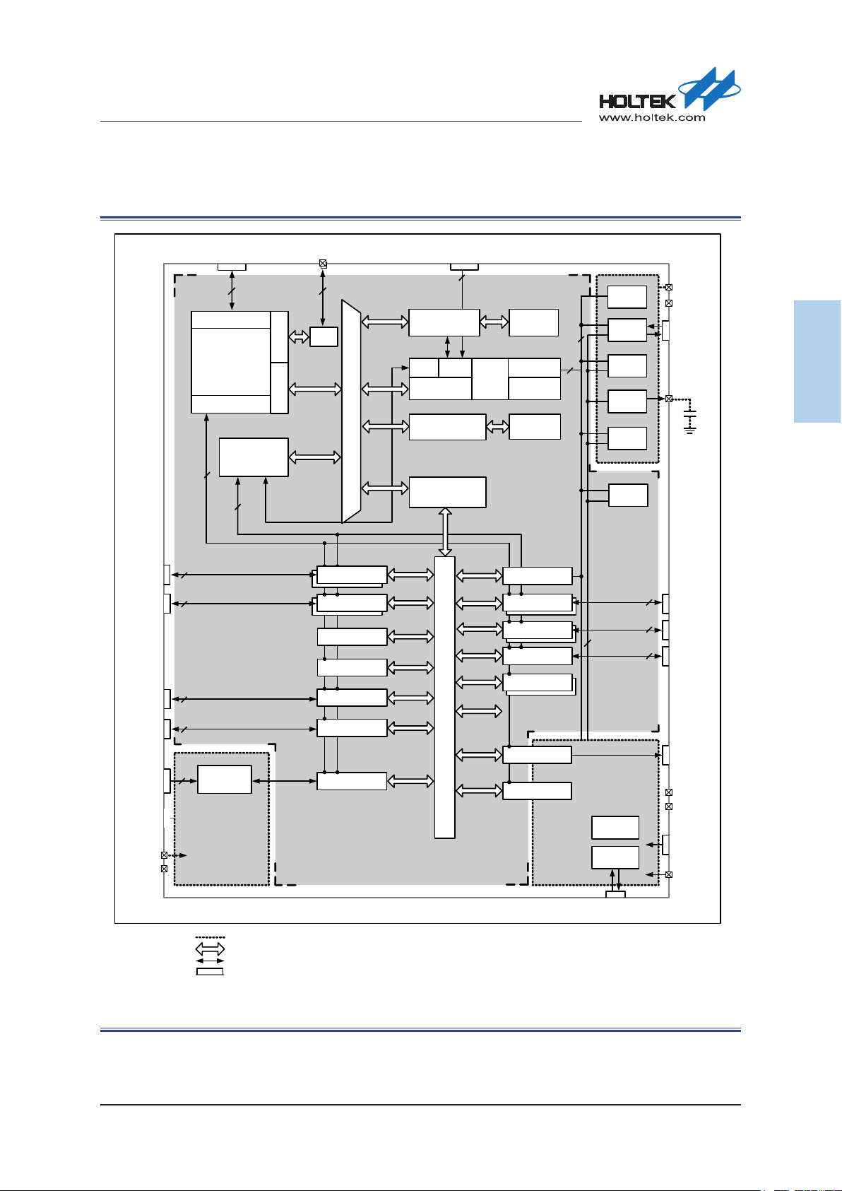
32-Bit Arm® Cortex®-M0+ MCU
HT32F52243/HT32F52253
Block Diagram
TX, RX
RTS/TXE
CTS/SCK
TX, RX
CH0 ~CH2
CH0N ~ CH2N
CH3, BRK
SCTM
ADC_IN0
AD C_I N11
V
V
DDA
PA ~ PC[15:0], PD[3:0]
IO Por t
GPIO
Syst em
U SA RT0 ~ 1
UART0 ~ 3
U AR T0
SCTM0 ~ 3
Powered by V
DD15
Bus Ma trix
AFIO
EXTI
MCTM
ADC
BOOT
Flash Memory
Interf ace
FMC
PDM A
Control
Control
Registers
Reg iste rs
AHB
Peripherals
SRAM
Controller
AHB to APB
Bridge
APB
CRC
-16/32
Powered by V
Flash
Memory
CKCU/R STCU
Contr ol Regi sters
Div ider
SRAM
WDT
SPI1 ~ 0
SPI1 ~ 0
I2C0 ~ 2
GPTM
BFTM0 ~ 1
RTC
PWRCU
Powered by V
DD15
Cl ock and res et co ntrol
DD
Powered by V
Pow er co ntrol
LSI
32 kHz
LSE
32,768 Hz
AF
X32KIN
X32KOUT
POR
/PD R
HSE
4 ~ 16 MHz
HSI
8 MHz
LDO
1.5 V
BOD
LVD
PLL
f
: 48 MH z
Max
DD
V
DD
V
SS
AF
XTALIN
XTALOUT
CLDO
AF
MOSI, MISO
SCK, SEL
AF
SDA
SCL
AF
CH3 ~ CH0
AF AF
RTCOUT
V
DD
V
SS
WAKEUP
nRST
Introduction
CAP.
SWCLK SWDIO
AF AF
SW-DP
Cortex®-M0+
Processor
NVIC
Interrupt request
PDMA
6 Channels
DMA request
AF
AF
AF
AF
AF
...
DDA
SSA
12- bit
SAR ADC
Powered by V
Power supply:
Bus:
Control signal:
Alternate function:
AF
Figure 1. Block Diagram
Rev. 1.20 28 of 501 September 19, 2018
Page 29
32-Bit Arm® Cortex®-M0+ MCU
HT32F52243/HT32F52253
2
Document Conventions
The conventions used in this document are shown in the following table.
Table 2. Document Conventions
Notation Example Description
0x 0x5a05
0xnnnn_nnnn 0x2000_0100 32-bit Hexadecimal address or data.
b b0101
NAME [n] ADDR [5]
NAME [m:n] ADDR [11:5]
X b10X1 Don’t care notation which means any value is allowed.
19 18
RW
RO
RC
WC
W0C
WO
Reserved
Word Data length of a word is 32-bit.
Half-word Data length of a half-word is 16-bit.
Byte Data length of a byte is 8-bit.
SERDYIE PLLRDYIE
RW 0 RW 0
3 2
HSIRDY HSERDY
RO 1 RO 0
1 0
PDF BAK_PORF
RC 0 RC 1
3 2
SERDYF PLLRDYF
WC 0 WC 0
1 0
RXCF PAPF
RO 0 W0C 0
31 30
DB_CKSRC
WO 0 WO 0
1 0
LLRDY Reserved
RO 0
The number string with a 0x prefix indicates a
hexadecimal number.
The number string with a lowercase b prex indicates a
binary number.
Specic bit of NAME. NAME can be a register or eld of
register. For example, ADDR [5] means bit 5 of ADDR
register (eld).
Specic bits of NAME. NAME can be a register or eld
of register. For example, ADDR [11:5] means bit 11 to 5
of ADDR register (eld).
Software can read and write to this bit.
Software can only read this bit. A write operation will
have no effect.
Software can only read this bit. Read operation will
clear it to 0 automatically.
Software can read this bit or clear it by writing 1. Writing
a 0 will have no effect.
Software can read this bit or clear it by writing 0. Writing
a 1 will have no effect.
Software can only write to this bit. A read operation
always returns 0.
Reserved bit(s) for future use. Data read from these bits
is not well defined and should be treated as random
data. Normally these reserved bits should be set to a
0 value. Note that reserved bit must be kept at reset
value.
Document Conventions
Rev. 1.20 29 of 501 September 19, 2018
Page 30

32-Bit Arm® Cortex®-M0+ MCU
HT32F52243/HT32F52253
3
System Architecture
The system architecture of devices that includes the Arm® Cortex®-M0+ processor, bus architecture
and memory organization will be described in the following sections. The Cortex®-M0+ is a next
generation processor core which offers many new features. Integrated and advanced features make
the Cortex®-M0+ processor suitable for market products that require microcontrollers with high
performance and low power consumption. In brief, The Cortex®-M0+ processor includes AHB-Lite
bus interface. All memory accesses of the Cortex®-M0+ processor are executed on the AHB-Lite
bus according to the different purposes and the target memory spaces. The memory organization
uses a Harvard architecture, pre-dened memory map and up to 4 GB of memory space, making
the system exible and extendable.
Arm® Cortex®-M0+ Processor
The Cortex®-M0+ processor is a very low gate count, highly energy efficient processor that is
intended for microcontroller and deeply embedded applications that require an area optimized,
low-power processor. The processor is based on the ARMv6-M architecture and supports Thumb®
instruction sets; single-cycle I/O port; hardware multiplier and low latency interrupt respond time.
Some system peripherals listed below are also provided by Cortex®-M0+:
▄
Internal Bus Matrix connected with AHB-Lite Interface, Single-cycle I/O port and Debug
Accesses Port (DAP)
▄
Nested Vectored Interrupt Controller (NVIC)
▄
Optional Wakeup Interrupt Controller (WIC)
▄
Breakpoint and Watchpoint Unit
▄
Optional Memory Protection Unit (MPU)
▄
Serial Wire debug Port (SW-DP)
▄
Optional Micro Trace Buffer Interface (MTB)
The following gure shows the Cortex®-M0+ processor block diagram. For more information, refer
to the Arm® Cortex®-M0+ Technical Reference Manual.
System Architecture
Rev. 1.20 30 of 501 September 19, 2018
Page 31

32-Bit Arm® Cortex®-M0+ MCU
HT32F52243/HT32F52253
Cortex-M0+ Components
Cortex®-M0+ Processor
Interrupts
‡ Wakeup
Interrupt
Controller (WIC)
‡ Optional Componect
Nested
Vectored
Interrupt
Controller
(NVIC)
Figure 2. Cortex®-M0+ Block Diagram
Bus Architecture
Execution Trace Interface
Cortex®-M0+
Processor
Core
‡ Memory
Protection
Unit
Bus Matrix
AHB-Lite Interface
to System
Debug
‡ Breakpoint
and
Watchpoint
Unit
‡ Debugger
Interface
‡ Single-cycle
I/O Port
System Architecture
‡ Debug
Access Port
(DAP)
‡ Serial Wire or JTAG
Debug Port
The HT32F52243/HT32F52253 series consist of one master and four slaves in the bus architecture.
The Cortex®-M0+ AHB-Lite bus is the master while the internal SRAM access bus, the internal
Flash memory access bus, the AHB peripherals access bus and the AHB to APB bridges are the
slaves. The single 32-bit AHB-Lite system interface provides simple integration to all system
regions include the internal SRAM region and the peripheral region. All of the master buses are
based on 32-bit Advanced High-performance Bus-Lite (AHB-Lite) protocol. The following gure
shows the bus architecture of the HT32F52243/HT32F52253 series.
Rev. 1.20 31 of 501 September 19, 2018
Page 32

32-Bit Arm® Cortex®-M0+ MCU
HT32F52243/HT32F52253
GPIO
Cortex®-M0+
Processor
Interrupt request
NVIC
PDMA
6 Channels
DMA request
I/O Port
System
Bus Matrix
Flash Memory Interface
PDMA
Control
Registers
AHB Peripherals
FMC
Control
Registers
SRAM Controller
AHB to APB
Bridge
GPIO
A~D
CRC
-16/32
Flash Memory
System Architecture
CKCU/RSTCU
Control Registers
SRAM
APB IPs
Figure 3. Bus Architecture
Memory Organization
The Arm® Cortex®-M0+ processor accesses and debug accesses share the single external
interface to external AHB peripheral. The processor accesses take priority over debug accesses.
The maximum address range of the Cortex®-M0+ is 4 GB since it has 32-bit bus address width.
Additionally, a pre-defined memory map is provided by the Cortex®-M0+ processor to reduce
the software complexity of repeated implementation of different device vendors. However, some
regions are used by the Arm® Cortex®-M0+ system peripherals. Refer to the Arm® Cortex®-M0+
Technical Reference Manual for more information. The following gure shows the memory map
of HT32F52243/HT32F52253 series of devices, including Code, SRAM, peripheral, and other pre-
dened regions.
Rev. 1.20 32 of 501 September 19, 2018
Page 33

32-Bit Arm® Cortex®-M0+ MCU
HT32F52243/HT32F52253
Memory Map
0xFFFF_FFFF
0xE010_0000
Private peripheral bus
16 KB on-chip SRAM
128 KB on-chip Flash
Peripheral
SRAM
Code
0xE000_0000
0x4010_0000
0x4008_0000
0x4000_0000
0x2000_4000
0x2000_0000
0x1FF0_0400
0x1FF0_0000
0x1F00_0800
0x1F00_0000
0x0001_0000
0x0000_0000
Reserved
Reserved
AHB peripherals
APB peripherals
Reserved
Reserved
Option byte alias
Reserved
Boot loader
Reserved
Up to
512 KB
512 KB
16 KB
1 KB
2 KB
Up to
128 KB
0x400F_FFFF
0x400C_C000
0x400C_A000
0x400B_8000
0x400B_0000
0x4009_2000
0x4008_C000
0x4007_8000
0x4007_7000
0x4007_6000
0x4007_5000
0x4007_4000
0x4006_F000
0x4006_E000
0x4006_B000
0x4006_A000
0x4006_9000
0x4006_8000
0x4005_9000
0x4004_A000
0x4004_9000
0x4004_8000
0x4004_5000
0x4004_4000
0x4004_3000
0x4004_2000
0x4004_1000
0x4004_0000
0x4003_6000
0x4003_5000
0x4003_4000
0x4002_D000
0x4002_C000
0x4002_5000
0x4002_4000
0x4002_3000
0x4002_2000
0x4001_1000
0x4001_0000
0x4000_9000
0x4000_8000
0x4000_5000
0x4000_4000
0x4000_3000
0x4000_2000
0x4000_1000
0x4000_0000
Reserved
DIV
Reserved
GPIO A ~ D
Reserved
PDMA_REG0x4009_0000
Reserved
CRC0x4008_A000
CKCU/RSTCU0x4008_8000
Reserved0x4008_2000
FMC0x4008_0000
Reserved
BFTM1
BFTM0
SCTM3
SCTM1
Reserved
GPTM0
Reserved
RTC & PWRCU
Reserved
WDT
Reserved
Reserved
I2C1
I2C0
Reserved
SPI1
Reserved
UART3
UART1
USART1
Reserved
SCTM2
SCTM0
Reserved
MCTM
Reserved
EXTI
Reserved
AFIO
Reserved
ADC
Reserved
I2C2
Reserved
SPI0
Reserved
UART2
UART0
USART0
System Architecture
AHB
APB
Figure 4. Memory Map
Rev. 1.20 33 of 501 September 19, 2018
Page 34

32-Bit Arm® Cortex®-M0+ MCU
HT32F52243/HT32F52253
Table 3. Register Map
Start Address End Address Peripheral Bus
0x4000_0000 0x4000_0FFF USART0
0x4000_1000 0x4000_1FFF UART0
0x4000_2000 0x4000_2FFF UART2
0x4000_3000 0x4000_3FFF Reserved
0x4000_4000 0x4000_4FFF SPI0
0x4000_5000 0x4000_7FFF Reserved
0x4000_8000 0x4000_8FFF I2C2
0x4000_9000 0x4000_FFFF Reserved
0x4001_0000 0x4001_0FFF ADC
0x4001_1000 0x4002_1FFF Reserved
0x4002_2000 0x4002_2FFF AFIO
0x4002_3000 0x4002_3FFF Reserved
0x4002_4000 0x4002_4FFF EXTI
0x4002_5000 0x4002_BFFF Reserved
0x4002_C000 0x4002_CFFF MCTM
0x4002_D000 0x4003_3FFF Reserved
0x4003_4000 0x4003_4FFF SCTM0
0x4003_5000 0x4003_5FFF SCTM2
0x4003_6000 0x4003_FFFF Reserved
0x4004_0000 0x4004_0FFF USART1
0x4004_1000 0x4004_1FFF UART1
0x4004_2000 0x4004_2FFF UART3
0x4004_3000 0x4004_3FFF Reserved
0x4004_4000 0x4004_4FFF SPI1
0x4004_5000 0x4004_7FFF Reserved
0x4004_8000 0x4004_8FFF I2C0
0x4004_9000 0x4004_9FFF I2C1
0x4004_A000 0x4006_7FFF Reserved
0x4006_8000 0x4006_8FFF WDT
0x4006_9000 0x4006_9FFF Reserved
0x4006_A000 0x4006_AFFF RTC/PWRCU
0x4006_B000 0x4006_DFFF Reserved
0x4006_E000 0x4006_EFFF GPTM
0x4006_F000 0x4007_3FFF Reserved
0x4007_4000 0x4007_4FFF SCTM1
0x4007_5000 0x4007_5FFF SCTM3
0x4007_6000 0x4007_6FFF BFTM0
0x4007_7000 0x4007_7FFF BFTM1
0x4007_8000 0x4007_FFFF Reserved
System Architecture
APB
Rev. 1.20 34 of 501 September 19, 2018
Page 35

32-Bit Arm® Cortex®-M0+ MCU
HT32F52243/HT32F52253
Start Address End Address Peripheral Bus
0x4008_0000 0x4008_1FFF FMC
0x4008_2000 0x4008_7FFF Reserved
0x4008_8000 0x4008_9FFF CKCU/RSTCU
0x4008_A000 0x4008_BFFF CRC
0x4008_C000 0x4008_FFFF Reserved
0x4009_0000 0x4009_1FFF PDMA_REG
0x4009_2000 0x400A_FFFF Reserved
0x400B_0000 0x400B_1FFF GPIOA
0x400B_2000 0x400B_3FFF GPIOB
0x400B_4000 0x400B_5FFF GPIOC
0x400B_6000 0x400B_7FFF GPIOD
0x400B_8000 0x400C_9FFF Reserved
0x400C_A000 0x400C_BFFF DIV
0x400C_C000 0x400F_FFFF Reserved
Embedded Flash Memory
The HT32F52243/HT32F52253 series provide up to 128 KB on-chip Flash memory which is
located at address 0x0000_0000. It supports byte, half-word, and word access operations. Note that
the Flash memory only supports read operations for the bus access. Any write operations to the
Flash memory will cause a bus fault exception. The Flash memory has up to capacity of 128 pages.
Each page has a memory capacity of 1 KB and can be erased independently. A 32-bit programming
interface provides the capability of changing bits from 1 to 0. A data storage or rmware upgrade
can be implemented using several methods such as In System Programming (ISP), In Application
Programming (IAP) or In Circuit Programming (ICP). For more information, refer to the Flash
Memory Controller section.
System Architecture
AHB
Embedded SRAM Memory
The HT32F52243/HT32F52253 series contain up to 16 KB on-chip SRAM which is located at
address 0x2000_0000. It support byte, half-word and word access operations.
AHB Peripherals
The address of the AHB peripherals ranges from 0x4008_0000 to 0x400F_FFFF. Some peripherals
such as Clock Control Unit, Reset Control Unit and Flash Memory Controller are connected to the
AHB bus directly. The AHB peripherals clocks are always enabled after a system reset. Access to
registers for these peripherals can be achieved directly via the AHB bus. Note that all peripheral
registers in the AHB bus support only word access.
APB Peripherals
The address of APB peripherals ranges from 0x4000_0000 to 0x4007_FFFF. An APB to AHB
Bridge provides access capability between the CPU and the APB peripherals. Additionally, the
APB peripheral clocks are disabled after a system reset. Software must enable the peripheral clock
by setting up the APBCCRn register in the Clock Control Unit before accessing the corresponding
peripheral register. Note that the APB to AHB Bridge will duplicate the half-word or byte data to
word width when a half-word or byte access is performed on the APB peripheral registers. In other
words, the access result of a half-word or byte access on the APB peripheral register will vary
depending on the data bit width of the access operation on the peripheral registers.
Rev. 1.20 35 of 501 September 19, 2018
Page 36

32-Bit Arm® Cortex®-M0+ MCU
HT32F52243/HT32F52253
4
Flash Memory Controller (FMC)
Introduction
The Flash Memory Controller (FMC) provides functions of ash operation and pre-fetch buffer for
the embedded on-chip Flash memory. The figure below shows the block diagram of FMC which
includes programming interface, control registers, pre-fetch buffer, and access interface. Since the
access speed of Flash memory is slower than the CPU, a wide access interface with pre-fetch buffer
is provided to the Flash memory in order to reduce the wait state (which will cause instruction
gaps) of the CPU. The functions of word program/page erase are also provided for instruction/data
storage of Flash memory.
AHB Peripheral Bus
System Bus
Flash Memory Controller
Control Register
Pre-fetch Buffer
Wait State
Control
Addressing
Data
Programming
Control
Flash Memory Controller (FMC)
Flash
Information
Block
Main Flash
Memory
Figure 5. Flash Memory Controller Block Diagram
Features
▄
Up to 128 KB of on-chip Flash memory for storing instruction/data and options
● 128 KB (instruction/data + Option Byte)
● 64 KB (instruction/data + Option Byte)
▄
Page size of 1K Byte, totally up to 128 pages depending on the main Flash size
▄
Wide access interface with pre-fetch buffer to reduce instruction gaps
▄
Page erase and mass erase capability
▄
32-bit word programming
▄
Interrupt capability when ready or error occurs
▄
Flash read protection to prevent illegal code/data access
▄
Page erase/program protection to prevent unexpected operation
Rev. 1.20 36 of 501 September 19, 2018
Page 37

32-Bit Arm® Cortex®-M0+ MCU
HT32F52243/HT32F52253
Functional Descriptions
Flash Memory Map
The following figure is the Flash memory map of the system. The address ranges from
0x0000_0000 to 0x1FFF_FFFF (0.5 GB). The address from 0x1F00_0000 to 0x1F00_07FF is
mapped to Boot Loader Block (2 KB). Additionally, the region addressed from 0x1FF0_0000 to
0x1FF0_03FF is the alias of Option Byte block (1 KB) which locates at the last page of the main
Flash physically. The memory mapping on system view is shown as below.
0x1FFF_FFFF
0x1FF0_0400
Flash Memory Controller (FMC)
Reserved
0x1FF0_0000
0x1F00_0800
0x1F00_0000
0x0000_0000
Figure 6. Flash Memory Map
Option Byte
Reserved
Boot Loader Block
Reserved
Main Flash Block
User Application
1 KB
2 KB
127 KB
or
64 KB
Rev. 1.20 37 of 501 September 19, 2018
Page 38

32-Bit Arm® Cortex®-M0+ MCU
HT32F52243/HT32F52253
Flash Memory Architecture
The Flash memory consists of up to 128 KB main Flash with 1 KB per page and 2 KB Information
Block for Boot Loader. The main Flash memory contains totally 128 pages (or 64 pages for 64 KB
device) which can be erased individually. The following table shows the base address, size, and
protection setting bit of each page.
Table 4. Flash Memory and Option Byte
Block Name Address
Page 0 0x0000_0000 ~ 0x0000_03FF OB_PP [0] 1 KB
Page 1 0x0000_0400 ~ 0x0000_07FF OB_PP [1] 1 KB
Page 2 0x0000_0800 ~ 0x0000_0BFF OB_PP [2] 1 KB
Page 3 0x0000_0C00 ~ 0x0000_0FFF OB_PP [3] 1 KB
Main Flash
Block
Page 124 0x0001_F000 ~ 0x0001_F3FF OB_PP [124] 1 KB
Page 125 0x0001_F400 ~ 0x0001_F7FF OB_PP [125] 1 KB
Page 126 0x0001_F800 ~ 0x0001_FBFF OB_PP [126] 1 KB
Page 127
(Option Byte)
Information
Block
Boot Loader 0x1F00_0000 ~ 0x1F00_07FF NA 2 KB
Page
Protection Bit
.
.
.
.
.
Physical: 0x0001_FC00 ~ 0x0001_FFFF
Alias: 0x1FF0_0000 ~ 0x1FF0_03FF
.
.
.
.
.
.
.
.
.
.
OB_CP [1] 1 KB
Size
.
.
.
.
.
Flash Memory Controller (FMC)
Notes:
1. The Information Block stores boot loader - this block can not be programmed or erased by
user.
2. The Option Byte is always located at last page of main Flash block.
Wait State Setting
When the HCLK clock is greater than the access speed of the Flash memory, the wait state cycles
must be inserted during the CPU fetch instructions or load data from Flash memory. The wait state
can be changed by setting the WAIT [1:0] of Flash Cache and Pre-fetch Control Register (CFCR).
In order to match the wait state requirement, the following two rules should be considered.
▄
HCLK clock is changed from lower to higher:
Change the wait state setting rst and then change the HCLK clock.
▄
HCLK clock is changed from higher to lower:
Change the HCLK clock rst and then change the wait state setting.
The following table shows the relationship between the wait state cycle and HCLK. The default
wait state is 0 since the HSI (8 MHz) is selected as the HCLK clock source after system reset.
Table 5. Relationship between wait state cycle and HCLK
Wait State Cycle HCLK
0 0 MHz < HCLK ≤ 20 MHz
1 20 MHz < HCLK ≤ 40 MHz
Rev. 1.20 38 of 501 September 19, 2018
Page 39

32-Bit Arm® Cortex®-M0+ MCU
HT32F52243/HT32F52253
Booting Conguration
The system provides two kinds of boot modes which can be selected using the BOOT pin. The
BOOT pin is sampled during a power-on reset or system reset. Once the logic value is decided, the
rst 4 words of vector will be remapped to the corresponding source according to the boot modes.
The boot mode is shown in the following table.
Table 6. Booting Modes
Boot mode selection pin
BOOT
0 Boot Loader The Vector source is Boot Loader
1 Main Flash The Vector source is main Flash
The Vector Mapping Control Register, VMCR, is provided to change the vector remapping setting
temporarily after the chip reset. The reset initial value of the VMCR register is determined by the
BOOT pin status which will be sampled during the reset duration.
Mode Descriptions
Flash Memory Controller (FMC)
Boot Setting
0xC
0x8
0x4
Hard Fault
Handler
NMI Handler
Program Counter
Initial Stack Point0x0
Figure 7. Vector Remapping
1 : Main Flash 0 : Boot Loader
+ 0xC
+ 0x8
+ 0x4
0x0000 0000
+ 0xC
+ 0x8
+ 0x4
0x1F00
0000
Rev. 1.20 39 of 501 September 19, 2018
Page 40

32-Bit Arm® Cortex®-M0+ MCU
HT32F52243/HT32F52253
Page Erase
The FMC provides a page erase function which is used to reset partial content of Flash memory.
Each page can be erased independently without affecting the contents of other pages. The following
steps show the access sequence of the register for a page erase operation.
▄
Check the OPCR register to conrm that no Flash memory operation is in progress (OPM [3:0]
equals to 0xE or 0x6). Otherwise, wait until the previous operation has been nished.
▄
Write the page address to TADR register.
▄
Write page erase command to the OCMR register (CMD [3:0] = 0x8).
▄
Commit the page erase command to the FMC by setting OPCR register (set OPM [3:0] = 0xA).
▄
Wait until all the operations have been completed by checking the value of the OPCR register
(OPM [3:0] equals to 0xE).
▄
Read and verify the page if required.
Note that a correct target page address must be conrmed. The Software may run out of control if
the target erase page is being used for fetching code or accessing data. The FMC will not provide
any notication when this happens. Additionally, the page erase will be ignored on the protected
pages. A Flash Operation Error interrupt will be triggered by the FMC if the OREIEN bit in
the OIER register is set. The software can check the PPEF bit in the OISR register to detect this
condition in the interrupt handler. The following gure shows the page erase operation ow.
Flash Memory Controller (FMC)
No
No
Start
Is OPM equal to
0xE or 0x6 ?
Yes
Set TADR, OCMR
Commit command
by setting OPCR
Is OPM equal to 0xE ?
Yes
Finish
Figure 8. Page Erase Operation Flowchart
Rev. 1.20 40 of 501 September 19, 2018
Page 41

32-Bit Arm® Cortex®-M0+ MCU
HT32F52243/HT32F52253
Mass Erase
The FMC provides a complete erase function which is used to initialize all the main Flash memory
contents to a high state. The following steps show the mass erase operation register access
sequence.
▄
Check the OPCR register to conrm that no Flash memory operation is in progress (OPM [3:0]
equals to 0xE or 0x6). Otherwise, wait until the previous operation has been nished.
▄
Write mass erase command to OCMR register (CMD [3:0] = 0xA).
▄
Commit the mass erase command to the FMC by setting the OPCR register (set OPM [3:0] = 0xA).
▄
Wait until all operations have been nished by checking the value of the OPCR register (OPM
[3:0] equals to 0xE).
▄
Read and verify the Flash memory if required.
Since all Flash data will be reset as 0xFFFF_FFFF, the mass erase operation can be implemented
by the program that runs in the SRAM or by the debugging tool that access the FMC register
directly. The software function that is executed on the Flash memory shall not trigger a mass erase
operation. The following gure shows the mass erase operation ow.
Flash Memory Controller (FMC)
No
No
Figure 9. Mass Erase Operation Flowchart
Is OPM equal to 0xE ?
Start
Is OPM equal to
0xE or 0x6 ?
Yes
Set OCMR = 0xA
Commit command
by setting OPCR
Yes
Finish
Rev. 1.20 41 of 501 September 19, 2018
Page 42

32-Bit Arm® Cortex®-M0+ MCU
HT32F52243/HT32F52253
Word Programming
The FMC provides a 32-bit word programming function which is used to modify the Flash memory
content. The following steps show the word programming operation register access sequence.
▄
Check the OPCR register to conrm that no Flash memory operation is in progress (OPM [3:0]
equals to 0xE, or 0x6). Otherwise, wait until the previous operation has been nished.
▄
Write the word address to the TADR register. Write the data to the WRDR register.
▄
Write the word program command to the OCMR register (CMD [3:0] = 0x4).
▄
Commit the word program command to the FMC by setting the OPCR register (set OPM [3:0] = 0xA).
▄
Wait until all operations have been nished by checking the value of the OPCR register (OPM
[3:0] equals to 0xE).
▄
Read and verify the Flash memory if required.
Note that the word programming operation can not be applied to the same address twice.
Successive word programming operation to the same address must be separated by a page erase
operation. Additionally, the word programming operation will be ignored on protected pages.
A Flash operation error interrupt will be triggered by the FMC if the OREIEN bit in the OIER
register is set. The software can check the PPEF bit in the OISR register to detect this condition in
the interrupt handler. The following gure shows the word programming operation ow.
Flash Memory Controller (FMC)
No
No
Start
Is OPM equal to
0xE or 0x6 ?
Yes
Set TADR, WRDR
and OCMR
Commit command
by setting OPCR
Is OPM equal to 0xE ?
Yes
Finish
Figure 10. Word Programming Operation Flowchart
Rev. 1.20 42 of 501 September 19, 2018
Page 43

32-Bit Arm® Cortex®-M0+ MCU
HT32F52243/HT32F52253
Option Byte Description
The Option Byte region can be treated as an independent Flash memory in which the base address
is 0x1FF0_0000. The following table shows the function description and the Option Byte memory
map.
Table 7. Option Byte Memory Map
Option Byte Offset Description Reset Value
Option Byte Base Address = 0x1FF0_0000
OB_PP
0x00C
OB_CP 0x010
OB_CK 0x020
0x000
0x004
0x008
Flash Page Erase/Program Protection (n = 0 ~ 127)
For HT32F52243
OB_PP [n] (n = 0 ~ 63)
0: Flash Page n Erase / Program Protection is
enabled
1: Flash Page n Erase / Program Protection is
disabled
OB_PP [n] (n = 64 ~ 127)
Reserved
For HT32F52253
OB_PP [n] (n = 0 ~ 126)
0: Flash Page n Erase / Program Protection is
enabled
1: Flash Page n Erase / Program Protection is
disabled
OB_PP [n] (n = 127)
Reserved
Flash Security Protection
OB_CP [0]
0: Flash Security protection is enabled
1: Flash Security protection is disabled
Option Byte Protection
OB_CP [1]
0: Option Byte protection is enabled
1: Option Byte protection is disabled
OB_CP [31:2]
Reserved
Flash Option Byte Checksum
OB_CK [31:0]
OB_CK should be set as the content value sum of 5
registers which offset address is form 0x000 to 0x010
in Option Byte (0x000 + 0x004 + 0x008 + 0x00C +
0x010) when the OB_PP or OB_CP register content
is not equal to 0xFFFF_FFFF. Otherwise, both page
erase/program protection and security protection will
be enabled.
Flash Memory Controller (FMC)
0xFFFF_FFFF
0xFFFF_FFFF
0xFFFF_FFFF
0xFFFF_FFFF
0xFFFF_FFFF
0xFFFF_FFFF
Rev. 1.20 43 of 501 September 19, 2018
Page 44

32-Bit Arm® Cortex®-M0+ MCU
HT32F52243/HT32F52253
Page Erase/Program Protection
The FMC provides page erase/program protection function to prevent unexpected operation of
Flash memory. The page erase (CMD [3:0] = 0x8 in the OCMR register) or word program (CMD
[3:0] = 0x4) command will not be accepted by FMC on the protected pages. When the page erase
or word programming command is sent to the FMC on a protected page, the PPEF bit in the OISR
register will then be set by the FMC and the Flash operation error interrupt will be triggered to
CPU by the FMC if the OREIEN bit in the OIER register is set. The page protection function can
be individually enabled for each page by conguring the OB_PP registers in the Option Byte. The
following table shows the access permission of the main Flash page when the page protection is
enabled.
Table 8. Access Permission of Protected Main Flash Page
Operation
Read O O
Program X X
Page Erase X X
Mass Erase O O
Mode
Flash Memory Controller (FMC)
ISP / IAP ICP / Debug mode
Notes:
1. The write protection is based on specic pages. The above access permission only affects
the pages of which the protection function has been enabled. Other pages are not affected.
2. Main Flash page protection is congured by the OB_PP [126:0]. Option Byte is physically
located at the last page of the main Flash. Option Byte page protection is congured by
the OB_CP [1] bit.
3. The page erase on the Option Byte area can disable the page protection of the main Flash.
4. The page protection of the Option Byte can only be disabled by a mass erase operation.
The following steps show the page erase/program protection procedure register access sequence.
▄
Check the OPCR register to conrm that no Flash memory operation is in program (OPM [3:0]
equals to 0xE or 0x6). Otherwise, wait until the previous operation has been nished.
▄
Write the OB_PP address to the TADR register (TADR = 0x1FF0_0000).
▄
Write the data which indicates the protection function of the corresponding page is enabled or
disabled into the WRDR register (0: Enabled, 1: Disabled).
▄
Write the word program command to the OCMR register (CMD [3:0] = 0x4).
▄
Commit the word program command to the FMC by setting the OPCR register (set OPM [3:0] =
0xA).
▄
Wait until all operations have been nished by checking the value of the OPCR register (OPM
[3:0] equals to 0xE).
▄
Read and verify the Option Byte if required.
▄
The OB_CK eld in the Option Byte must be updated according to the Option Byte checksum
rule.
▄
Apply a system reset to activate the new OB_PP setting.
Rev. 1.20 44 of 501 September 19, 2018
Page 45

32-Bit Arm® Cortex®-M0+ MCU
HT32F52243/HT32F52253
Security Protection
The FMC provides a Security protection function to prevent illegal code/data access of the Flash
memory. This function is useful for protecting the software / rmware from the illegal users. The
function is activated by conguring the Option Byte OB_CP [0] bit. Once the function has been
enabled, all the main Flash data access through ICP/Debug mode, programming, and page erase
operation will not be allowed except the user’s application. However, the mass erase operation will
still be accepted by the FMC in order to disable this security protection function. The following
table shows the access permission of the Flash memory when the security protection is enabled.
Table 9. Access Permission When Security Protection is Enabled
Operation
Read O X (read as 0)
Program O
Page Erase O
Mass Erase O O
Notes:
1. User application means the software that is executed or booted from main Flash memory
with the JTAG/SW debugger being disconnected. However, the Option Byte block and
page 0 are still in protection in which the Program/Page Erase can not be executed.
2. The Mass erase operation can erase the Option Byte block and disable the security protection.
The following steps show the Security protection procedure register access sequence.
Mode
User application
(1)
(1)
(1)
ICP/Debug mode
X
X
(2)
Flash Memory Controller (FMC)
▄
Check the OPCR register to conrm that no Flash memory operation is in progress (OPM [3:0]
equal to 0xE or 0x6). Otherwise, wait until the previous operation has been nished.
▄
Write the OB_CP address to the TADR register (TADR = 0x1FF0_0010).
▄
Write the data into the WRDR register to set OB_CP [0] to 0.
▄
Write the word program command to the OCMR register (CMD [3:0] = 0x4).
▄
Commit the word program command to the FMC by setting the OPCR register (set OPM = 0xA).
▄
Wait until all operations have been nished by checking the value of the OPCR register (OPM
[3:0] equals to 0xE).
▄
Read and verify the Option Byte if required.
▄
The OB_CK eld in the Option Byte must be updated according to the Option Byte checksum rule.
▄
Apply a system reset to activate the new OB_CP setting.
Rev. 1.20 45 of 501 September 19, 2018
Page 46

32-Bit Arm® Cortex®-M0+ MCU
HT32F52243/HT32F52253
Register Map
The following table shows the FMC registers and reset values.
Table 10. FMC Register Map
Register Offset Description Reset Value
FMC Base Address = 0x4008_0000
TADR 0x000 Flash Target Address Register 0x0000_0000
WRDR 0x004 Flash Write Data Register 0x0000_0000
OCMR 0x00C Flash Operation Command Register 0x0000_0000
OPCR 0x010 Flash Operation Control Register 0x0000_000C
OIER 0x014 Flash Operation Interrupt Enable Register 0x0000_0000
OISR 0x018 Flash Operation Interrupt and Status Register 0x0001_0000
0x020
PPSR
CPSR 0x030 Flash Security Protection Status Register 0x0000_00XX
VMCR 0x100 Flash Vector Mapping Control Register 0x0000_000X
MDID 0x180 Flash Manufacturer and Device ID Register 0x0376_XXXX
PNSR 0x184 Flash Page Number Status Register 0x0000_00XX
PSSR 0x188 Flash Page Size Status Register 0x0000_0400
DIDR 0x18C Device ID Register 0x000X_XXXX
CFCR 0x200 Flash Pre-fetch Control Register 0x0000_0051
CIDR0 0x310 Custom ID Register 0 0xXXXX_XXXX
CIDR1 0x314 Custom ID Register 1 0xXXXX_XXXX
CIDR2 0x318 Custom ID Register 2 0xXXXX_XXXX
CIDR3 0x31C Custom ID Register 3 0xXXXX_XXXX
0x024
0x028
0x02C
Flash Page Erase/Program Protection Status
Register
Flash Memory Controller (FMC)
0xXXXX_XXXX
0xXXXX_XXXX
0xXXXX_XXXX
0xXXXX_XXXX
Note:
"X" means various reset values which depend on the Device, Flash value, Option Byte value,
or power on reset setting.
Rev. 1.20 46 of 501 September 19, 2018
Page 47

32-Bit Arm® Cortex®-M0+ MCU
HT32F52243/HT32F52253
Register Descriptions
Flash Target Address Register – TADR
This register species the target address of the page erase and word programming operations.
Offset: 0x000
Reset value: 0x0000_0000
31 30 29 28 27 26 25 24
TADB
Type/Reset RW 0 RW 0 RW 0 RW 0 RW 0 RW 0 RW 0 RW 0
23 22 21 20 19 18 17 16
TADB
Type/Reset RW 0 RW 0 RW 0 RW 0 RW 0 RW 0 RW 0 RW 0
15 14 13 12 11 10 9 8
TADB
Type/Reset RW 0 RW 0 RW 0 RW 0 RW 0 RW 0 RW 0 RW 0
7 6 5 4 3 2 1 0
TADB
Type/Reset RW 0 RW 0 RW 0 RW 0 RW 0 RW 0 RW 0 RW 0
Flash Memory Controller (FMC)
Bits Field Descriptions
[31:0] TADB Flash Target Address Bits
For programming operations, the TADR register species the address where the
data is written. Since the programming length is 32-bit, the TADR should be set as
word-aligned (4 bytes). The TADB [1:0] bits will be ignored during programming
operations. For page erase operations, the TADR register contains the page
address which is going to be erased. Since the page size is 1 KB, the TADB [9:0]
will be ignored in order to limit the target address as 1 Kbyte-aligned. For 128 KB
main Flash addressing, the TADB [31:17] should be zero while the TADB [31:16]
should be zero for 64 KB main Flash addressing. The region of which the address
ranges from 0x1FF0_0000 to 0x1FF0_03FF is the 1KB Option Byte. This field
for available Flash address must be under 0x1FFF_FFFF. Otherwise, the Invalid
Target Address interrupt will occur if the corresponding interrupt enable bit is set.
Rev. 1.20 47 of 501 September 19, 2018
Page 48

32-Bit Arm® Cortex®-M0+ MCU
HT32F52243/HT32F52253
Flash Write Data Register – WRDR
This register species the data to be written for programming operation.
Offset: 0x004
Reset value: 0x0000_0000
31 30 29 28 27 26 25 24
WRDB
Type/Reset RW 0 RW 0 RW 0 RW 0 RW 0 RW 0 RW 0 RW 0
23 22 21 20 19 18 17 16
WRDB
Type/Reset RW 0 RW 0 RW 0 RW 0 RW 0 RW 0 RW 0 RW 0
15 14 13 12 11 10 9 8
WRDB
Type/Reset RW 0 RW 0 RW 0 RW 0 RW 0 RW 0 RW 0 RW 0
7 6 5 4 3 2 1 0
WRDB
Type/Reset RW 0 RW 0 RW 0 RW 0 RW 0 RW 0 RW 0 RW 0
Flash Memory Controller (FMC)
Bits Field Descriptions
[31:0] WRDB Flash Write Data Bits
The data value for programming operation.
Rev. 1.20 48 of 501 September 19, 2018
Page 49

32-Bit Arm® Cortex®-M0+ MCU
HT32F52243/HT32F52253
Flash Operation Command Register – OCMR
This register is used to specify the Flash operation commands that include the word programming, page erase
and mass erase.
Offset: 0x00C
Reset value: 0x0000_0000
31 30 29 28 27 26 25 24
Reserved
Type/Reset
23 22 21 20 19 18 17 16
Reserved
Type/Reset
15 14 13 12 11 10 9 8
Reserved
Type/Reset
7 6 5 4 3 2 1 0
Reserved CMD
Type/Reset RW 0 RW 0 RW 0 RW 0
Bits Field Descriptions
[3:0] CMD Flash Operation Command
The following table shows the definitions of the operation command bits, CMD
[3:0], which specify the Flash memory operation. If an invalid command is set and
the IOCMIEN bit is set to 1, an Invalid Operation Command interrupt will occur.
CMD [3:0] Description
0x0 Idle (default)
0x4 Word program
0x8 Page erase
0xA Mass erase
Others Reserved
Flash Memory Controller (FMC)
Rev. 1.20 49 of 501 September 19, 2018
Page 50

32-Bit Arm® Cortex®-M0+ MCU
HT32F52243/HT32F52253
Flash Operation Control Register – OPCR
This register is used for controlling the command commitment and checking the status of the FMC operations.
Offset: 0x010
Reset value: 0x0000_000C
31 30 29 28 27 26 25 24
Reserved
Type/Reset
23 22 21 20 19 18 17 16
Reserved
Type/Reset
15 14 13 12 11 10 9 8
Reserved
Type/Reset
7 6 5 4 3 2 1 0
Reserved OPM Reserved
Type/Reset RW 0 RW 1 RW 1 RW 0
Flash Memory Controller (FMC)
Bits Field Descriptions
[4:1] OPM Operation Mode
The following table shows the operation mode of the FMC. User can commit the
command which is set by the OCMR register to the main ash according to the
address alias setting in the TADR register. The content of the TADR, WRDR,
and OCMR registers should be prepared before setting this register. After all the
operations have been nished, the OPM eld will be set as 0xE or 0xF by the FMC
hardware. The Idle mode can be set when all the operations have been nished
for power saving purpose. Note that the operation status should be checked before
the next operation is executed to the FMC. The contents of the TADR, WRDR,
OCMR, and OPCR registers should not be changed until the previous operation
has been nished.
OPM [3:0] Description
0x6 Idle (default)
0xA Commit command to main Flash
0xE All operation nished on main Flash
Others Reserved
Rev. 1.20 50 of 501 September 19, 2018
Page 51

32-Bit Arm® Cortex®-M0+ MCU
HT32F52243/HT32F52253
Flash Operation Interrupt Enable Register – OIER
This register is used to enable or disable the FMC interrupt function. The FMC generates interrupts to the
controller when corresponding interrupt enable bits are set.
Offset: 0x014
Reset value: 0x0000_0000
31 30 29 28 27 26 25 24
Reserved
Type/Reset
23 22 21 20 19 18 17 16
Reserved
Type/Reset
15 14 13 12 11 10 9 8
Reserved
Type/Reset
7 6 5 4 3 2 1 0
Reserved OREIEN IOCMIEN OBEIEN ITADIEN ORFIEN
Type/Reset RW 0 RW 0 RW 0 RW 0 RW 0
Bits Field Descriptions
[4] OREIEN Operation Error Interrupt Enable
0: Operation error interrupt is disabled
1: Operation error interrupt is enabled
[3] IOCMIEN Invalid Operation Command Interrupt Enable
0: Invalid Operation Command interrupt is disabled
1: Invalid Operation Command interrupt is enabled
[2] OBEIEN Option Byte Check Sum Error Interrupt Enable
0: Option Byte Check Sum Error interrupt is disabled
1: Option Byte Check Sum Error interrupt is enabled
[1] ITADIEN Invalid Target Address Interrupt Enable
0: Invalid Target Address interrupt is disabled
1: Invalid Target Address interrupt is enabled
[0] ORFIEN Operation Finished Interrupt Enable
0: Operation Finish interrupt is disabled
1: Operation Finish interrupt is enabled
Flash Memory Controller (FMC)
Rev. 1.20 51 of 501 September 19, 2018
Page 52

32-Bit Arm® Cortex®-M0+ MCU
HT32F52243/HT32F52253
Flash Operation Interrupt and Status Register – OISR
This register indicates the FMC interrupt status which is used to check if a Flash operation has been nished or
an error occurs. The status bits, bit [4:0], are available when the corresponding bits in the OIER register are set.
Offset: 0x018
Reset value: 0x0001_0000
31 30 29 28 27 26 25 24
Reserved
Type/Reset
23 22 21 20 19 18 17 16
Reserved PPEF RORFF
Type/Reset RO 0 RO 1
15 14 13 12 11 10 9 8
Reserved
Type/Reset
7 6 5 4 3 2 1 0
Reserved OREF IOCMF OBEF ITADF ORFF
Type/Reset WC 0 WC 0 WC 0 WC 0 WC 0
Bits Field Descriptions
[17] PPEF Page Erase/Program Protected Error Flag
0: Page Erase/Program Protected Error does not occur
1: Operation error occurs due to an invalid erase/program operation being
applied to a protected page
This bit is reset by hardware once a new ash operation command is committed.
[16] RORFF Raw Operation Finished Flag
0: The last ash operation command is not nished
1: The last ash operation command is nished
The RORFF bit is directly connected to the Flash memory for debugging purpose.
[4] OREF Operation Error Flag
0: No ash operation error occurred
1: The last ash operation is failed
This bit will be set when any flash operation error occurs such as an invalid
command, program error and erase error, etc. The ORE interrupt occurs if the
OREIEN bit in the OIER register is set. Reset this bit by writing 1.
[3] IOCMF Invalid Operation Command Flag
0: No invalid ash operation command was set
1: An invalid ash operation command has been written into the OCMR register.
The IOCM interrupt will be occurred if the IOCMIEN bit in the OIER register is set.
Reset this bit by writing 1.
[2] OBEF Option Byte Checksum Error Flag
0: Option Byte Checksum is correct
1: Option Byte Checksum is incorrect
The OBE interrupt will occur if the OBEIEN bit in the OIER register is set. This bit
is cleared to 0 by software writing 1 into it. However, the Option Byte Checksum
Error Flag can not be cleared by software until the interrupt condition is cleared
which means that the Option Byte checksum value has to be correctly modied or
the corresponding interrupt enable control is disabled. Otherwise, the interrupt will
be continually generated.
Flash Memory Controller (FMC)
Rev. 1.20 52 of 501 September 19, 2018
Page 53

32-Bit Arm® Cortex®-M0+ MCU
HT32F52243/HT32F52253
Bits Field Descriptions
[1] ITADF Invalid Target Address Flag
0: The target address is valid
1: The target address is invalid
The data in the TADR field must be within the range from 0x0000_0000 to
0x1FFF_FFFF. Otherwise, an ITAD interrupt will be generated if the ITADIEN bit in
the OIER register is set. Reset this bit by writing 1.
[0] ORFF Operation Finished Flag
0: Operation is not nished
1: Last Flash operation is nished
The ORF interrupt will be generated if the ORFIEN bit in the OIER register is set.
Reset this bit by writing 1.
Flash Page Erase/Program Protection Status Register – PPSR
This register indicates the page protection status of the Flash page erase/program protection functions.
Offset: 0x020 (0) ~ 0x02C (3)
Reset value: 0xXXXX_XXXX
Flash Memory Controller (FMC)
31 30 29 28 27 26 25 24
PPSBn
Type/Reset RO X RO X RO X RO X RO X RO X RO X RO X
23 22 21 20 19 18 17 16
PPSBn
Type/Reset RO X RO X RO X RO X RO X RO X RO X RO X
15 14 13 12 11 10 9 8
PPSBn
Type/Reset RO X RO X RO X RO X RO X RO X RO X RO X
7 6 5 4 3 2 1 0
PPSBn
Type/Reset RO X RO X RO X RO X RO X RO X RO X RO X
Bits Field Descriptions
[127:0] PPSBn Page Erase/Program Protection Status Bits (n = 0 ~ 127)
PPSB[n] = OB_PP[n]
0: The corresponding page n is protected
1: The corresponding page n is not protected
The content of this register is not dynamically updated and will only be reloaded
from the Option Byte when any kind of reset occurs. The erase or program
function of the specic pages are not allowed when the corresponding bits of the
PPSR register are reset to zero. The reset value of PPSR [127:0] is determined by
the Option Byte OB_PP [127:0] bits. Since the maximum page number of the main
flash is various and dependent on the chip specification. Therefore, each page
erase/program protection status bit may protect one or two pages, which depends
upon the chip specification. Other bits of the OB_PP and PPSR registers are
reserved for future usage.
Rev. 1.20 53 of 501 September 19, 2018
Page 54

32-Bit Arm® Cortex®-M0+ MCU
HT32F52243/HT32F52253
Flash Security Protection Status Register – CPSR
This register indicates the Flash Memory Security protection status. The content of this register is not dynamically
updated and will only be reloaded by the Option Byte loader which is active when any kind of reset occurs.
Offset: 0x030
Reset value: 0x0000_00XX
31 30 29 28 27 26 25 24
Reserved
Type/Reset
23 22 21 20 19 18 17 16
Reserved
Type/Reset
15 14 13 12 11 10 9 8
Reserved
Type/Reset
7 6 5 4 3 2 1 0
Reserved OBPSB CPSB
Type/Reset RO X RO X
Bits Field Descriptions
[1] OBPSB Option Byte Page Erase/Program Protection Status Bit
0: The Option Byte page is protected.
1: The Option Byte page is not protected.
The reset value of the OPBSB is determined by the Option Byte, OB_CP [1] bit.
[0] CPSB Flash Memory Security Protection Status Bit
0: Flash Memory Security protection is enabled
1: Flash Memory Security protection is not enabled
The reset value of the CPSB is determined by the Option Byte, OB_CP [0] bit.
Flash Memory Controller (FMC)
Rev. 1.20 54 of 501 September 19, 2018
Page 55

32-Bit Arm® Cortex®-M0+ MCU
HT32F52243/HT32F52253
Flash Vector Mapping Control Register – VMCR
This register is used to control the vector mapping. The reset value of the VMCR register is determined by the
external booting pin, BOOT, during the power-on reset period.
Offset: 0x100
Reset value: 0x0000_000X
31 30 29 28 27 26 25 24
Reserved
Type/Reset
23 22 21 20 19 18 17 16
Reserved
Type/Reset
15 14 13 12 11 10 9 8
Reserved
Type/Reset
7 6 5 4 3 2 1 0
Reserved VMCB Reserved
Type/Reset RW X
Bits Field Descriptions
[1] VMCB Vector Mapping Control Bit
The VMCB bit is used to control the mapping source of first 4-word vectors
addressed from 0x0 ~ 0xC. The following table shows the vector mapping setting.
BOOT VMCB [1] Descriptions
Low 0
High 1
The reset value of the VMCB bit is determined by the pin status of the external
BOOT pin during power-on reset and system reset. The vector mapping setting
can be changed temporarily by configuring the VMCB bit when the application
program is executed.
Boot Loader mode
The vector mapping source is the boot loader area.
Main Flash mode
The vector mapping source is the main Flash area.
Flash Memory Controller (FMC)
Rev. 1.20 55 of 501 September 19, 2018
Page 56

32-Bit Arm® Cortex®-M0+ MCU
HT32F52243/HT32F52253
Flash Manufacturer and Device ID Register – MDID
This register is used to store the manufacture ID and device part number information which can be used as the
product identity.
Offset: 0x180
Reset value: 0x0376_XXXX
31 30 29 28 27 26 25 24
MFID
Type/Reset RO 0 RO 0 RO 0 RO 0 RO 0 RO 0 RO 1 RO 1
23 22 21 20 19 18 17 16
MFID
Type/Reset RO 0 RO 1 RO 1 RO 1 RO 0 RO 1 RO 1 RO 0
15 14 13 12 11 10 9 8
ChipID
Type/Reset RO X RO X RO X RO X RO X RO X RO X RO X
7 6 5 4 3 2 1 0
ChipID
Type/Reset RO X RO X RO X RO X RO X RO X RO X RO X
Bits Field Descriptions
[31:16] MFID Manufacturer ID
Read as 0x0376
[15:0] ChipID Chip ID
Read the last 4 digital code of the MCU device part number
Flash Memory Controller (FMC)
Rev. 1.20 56 of 501 September 19, 2018
Page 57

32-Bit Arm® Cortex®-M0+ MCU
HT32F52243/HT32F52253
Flash Page Number Status Register – PNSR
This register is used to indicate the Flash memory page number.
Offset: 0x184
Reset value: 0x0000_00XX
31 30 29 28 27 26 25 24
PNSB
Type/Reset RO 0 RO 0 RO 0 RO 0 RO 0 RO 0 RO 0 RO 0
23 22 21 20 19 18 17 16
PNSB
Type/Reset RO 0 RO 0 RO 0 RO 0 RO 0 RO 0 RO 0 RO 0
15 14 13 12 11 10 9 8
PNSB
Type/Reset RO 0 RO 0 RO 0 RO 0 RO 0 RO 0 RO 0 RO 0
7 6 5 4 3 2 1 0
PNSB
Type/Reset RO X RO X RO X RO X RO X RO X RO X RO X
Flash Memory Controller (FMC)
Bits Field Descriptions
[31:0] PNSB Flash Page Number Status Bits
0x0000_0010: Totally 16 pages for the on-chip Flash memory device.
0x0000_0020: Totally 32 pages for the on-chip Flash memory device.
0x0000_0040: Totally 64 pages for the on-chip Flash memory device.
0x0000_0080: Totally 128 pages for the on-chip Flash memory device.
0x0000_00FF: Totally 255 pages for the on-chip Flash memory device.
They indicated the total page number of the on-chip Flash memory device.
Rev. 1.20 57 of 501 September 19, 2018
Page 58

32-Bit Arm® Cortex®-M0+ MCU
HT32F52243/HT32F52253
Flash Page Size Status Register – PSSR
This register is used to indicate the page size in bytes.
Offset: 0x188
Reset value: 0x0000_0400
31 30 29 28 27 26 25 24
PSSB
Type/Reset RO 0 RO 0 RO 0 RO 0 RO 0 RO 0 RO 0 RO 0
23 22 21 20 19 18 17 16
PSSB
Type/Reset RO 0 RO 0 RO 0 RO 0 RO 0 RO 0 RO 0 RO 0
15 14 13 12 11 10 9 8
PSSB
Type/Reset RO 0 RO 0 RO 0 RO 0 RO 0 RO 1 RO 0 RO 0
7 6 5 4 3 2 1 0
PSSB
Type/Reset RO 0 RO 0 RO 0 RO 0 RO 0 RO 0 RO 0 RO 0
Flash Memory Controller (FMC)
Bits Field Descriptions
[31:0] PSSB Flash Page Size Status Bits
0x200: The page size is 512 Byte per page.
0x400: The page size is 1 KB per page.
0x800: The page size is 2 KB per page.
Device ID Register – DIDR
This register is used to store the device part number information which can be used as the product identity.
Offset: 0x18C
Reset value: 0x000X_XXXX
31 30 29 28 27 26 25 24
Reserved
Type/Reset
23 22 21 20 19 18 17 16
Reserved ChipID
Type/Reset RO X RO X RO X RO X
15 14 13 12 11 10 9 8
ChipID
Type/Reset RO X RO X RO X RO X RO X RO X RO X RO X
7 6 5 4 3 2 1 0
ChipID
Type/Reset RO X RO X RO X RO X RO X RO X RO X RO X
Bits Field Descriptions
[19:0] ChipID Chip ID
Read the complete 5 digital code of the MCU device part number.
Rev. 1.20 58 of 501 September 19, 2018
Page 59

32-Bit Arm® Cortex®-M0+ MCU
HT32F52243/HT32F52253
Flash Pre-fetch Control Register – CFCR
This register is used for controlling the FMC pre-fetch module.
Offset: 0x200
Reset value: 0x0000_0011
31 30 29 28 27 26 25 24
Reserved
Type/Reset
23 22 21 20 19 18 17 16
Reserved
Type/Reset
15 14 13 12 11 10 9 8
Reserved
Type/Reset
7 6 5 4 3 2 1 0
Reserved PFBE Reserved WAIT
Type/Reset RW 1 RW 0 RW 0 RW 1
Flash Memory Controller (FMC)
Bits Field Descriptions
[4] PFBE Pre-fetch Buffer Enable Bit
0: Pre-fetch buffer is disabled.
1: Pre-fetch buffer is enabled (default).
The pre-fetch buffer is enabled in default. When the pre-fetch buffer is disabled,
the instruction and data are directly provided by the Flash memory.
[2:0] WAIT Flash Wait State Setting
The WAIT[2:0] eld is used to set the HCLK wait clock during a non-sequential
address Flash access. The actual wait clock is given by (WAIT[2:0] - 1). Since
a wide access interface with a pre-fetch buffer is provided, the wait state of
sequential Flash access is very close to zero.
WAIT [2:0] Wait Status Allowed HCLK Range
001 0 0 MHz < HCLK ≤ 20 MHz
010 1 20 MHz < HCLK ≤ 40 MHz
Others Reserved Reserved
Rev. 1.20 59 of 501 September 19, 2018
Page 60

32-Bit Arm® Cortex®-M0+ MCU
HT32F52243/HT32F52253
Custom ID Register n – CIDRn (n = 0 ~ 3)
This register is used to store the custom ID information which can be used as the custom identity.
Offset: 0x310 (0) ~ 0x31C (3)
Reset value: Various depending on Flash Manufacture Privilege Information Block.
31 30 29 28 27 26 25 24
CID
Type/Reset RO X RO X RO X RO X RO X RO X RO X RO X
23 22 21 20 19 18 17 16
CID
Type/Reset RO X RO X RO X RO X RO X RO X RO X RO X
15 14 13 12 11 10 9 8
CID
Type/Reset RO X RO X RO X RO X RO X RO X RO X RO X
7 6 5 4 3 2 1 0
CID
Type/Reset RO X RO X RO X RO X RO X RO X RO X RO X
Flash Memory Controller (FMC)
Bits Field Descriptions
[31:0] CIDn Custom ID
Read as the CIDn[31:0] (n = 0 ~ 3) field in the Custom ID registers in Flash
Manufacture Privilege Block.
Rev. 1.20 60 of 501 September 19, 2018
Page 61

32-Bit Arm® Cortex®-M0+ MCU
HT32F52243/HT32F52253
5
Power Control Unit (PWRCU)
Introduction
The power consumption can be regarded as one of the most important issues for many embedded
system applications. Accordingly the Power Control Unit, PWRCU, provides many types of power
saving modes such as Sleep, Deep-Sleep1, Deep-Sleep2, and Power-Down modes. These modes
reduce the power consumption and allow the application to achieve the best trade-off between the
conicting demands of CPU operating time, speed and power consumption. The dash line in the
Figure 11 indicates the power supply source of two digital power domains.
V
DD
nRST
WAKEUP
RTCOUT
RTC
LSI
LSE
WKUP1
WKUP2
WKUP3
HSE
PWR_CTRL
LDOOFF
LCM
DMOSON
WKUP4
SLEEPDEEP
SLEEPING
VDDDomain
LDO
DMOS
V
1.5 V Domain
DD15
CPU Memories
APB
INTF
Digital
Peripheral
HSI
3.3 V
POR/PDR
LVD
1.5 V
POR/PDR
PLL
Power Control Unit (PWRCU)
V
LDOOUT
V
DD15
LDO: Voltage Regulator
DMOS: Depletion MOS
Figure 11. PWRCU Block Diagram
LVD: Low Voltage Detector
POR/PDR: Power On Reset/Power Down Reset
Rev. 1.20 61 of 501 September 19, 2018
Page 62

32-Bit Arm® Cortex®-M0+ MCU
HT32F52243/HT32F52253
Features
▄
Two power domains: VDD 3.3 V and V
▄
Four power saving modes: Sleep, Deep-Sleep1, Deep-Sleep2 and Power-Down modes.
▄
Internal Voltage regulator supplies 1.5 V voltage source.
▄
Additional Depletion MOS supplies 1.5 V voltage source with low leakage and low operating
current.
▄
A power reset is generated when one of the following events occurs:
● Power-on / Power-down reset (POR / PDR reset).
● When exiting Power-Down mode.
● The control bits BODEN = 1, BODRIS = 0 and the supply power VDD ≤ V
▄
BOD Brown Out Detector can issue a system reset or an interrupt when VDD power source is
lower than the Brown Out Detector voltage V
▄
LVD Low Voltage Detector can issue an interrupt or wakeup event when VDD is lower than a
programmable threshold voltage V
1.5 V power domains.
DD15
BOD
.
LVD
Power Control Unit (PWRCU)
.
BOD
.
Functional Descriptions
VDD Power Domain
LDO Power Control
The LDO will be automatically switched off when one of the following conditions occurs:
▄
The Power-Down or Deep-Sleep 2 mode is entered.
▄
The control bits BODEN = 1, BODRIS = 0 and the supply power VDD ≤ V
▄
The supply power VDD ≤ V
The LDO will be automatically switched on by hardware when the supply power VDD > V
of the following conditions occurs:
▄
Resume operation from the power saving mode - RTC wakeup, LVD wakeup and WAKEUP pin
rising edge.
▄
Detect a falling edge on the external reset pin (nRST).
▄
The control bit BODEN = 1 and the supply power VDD > V
To enter the Deep-Sleep1 mode, the PWRCU will request the LDO to operate in a low current
mode, LCM. To enter the Deep-Sleep 2 mode, the PWRCU will turn off the LDO and turn on the
DMOS to supply an alternative 1.5 V power.
Voltage Regulator
The voltage regulator, LDO, Depletion MOS, DMOS, Low voltage Detector, LVD, High Speed
Internal oscillator, HSS, Low Speed Internal RC oscillator, LSI, and the Low Speed External
Crystal oscillator, LSE are operated under the VDD power domain. The LDO can be congured to
operate in either normal mode (LDOOFF = 0, LDOLCM = 0, I
current mode (LDOOFF = 0, LDOLCM =1, I
An alternative 1.5 V power source is the output of the DMOS which has low static and driving
current characteristics. It is controlled using the DMOSON bit in the BAKCR register. The DMOS
output has weak output current and regulation capability and only operate in the Deep-Sleep 2
mode for data retention purposes in the V
PDR
= Low current mode) to supply the 1.5 V power.
OUT
power domain.
DD15
.
BOD
.
BOD
= High current mode) or low
OUT
POR
if any
Rev. 1.20 62 of 501 September 19, 2018
Page 63

32-Bit Arm® Cortex®-M0+ MCU
HT32F52243/HT32F52253
Power On Reset (POR) / Power Down Reset (PDR)
The device has an integrated POR/PDR circuitry that allows proper operation starting from/down
to 2.0 V. The device remains in Power-Down mode when VDD is below a specied threshold V
without the need for an external reset circuit. For more details the power on / power down reset
threshold voltage, refer to the electrical characteristics of the corresponding datasheet.
V
DD
,
PDR
Power Control Unit (PWRCU)
V
POR
Hysteresis
V
PDR
POR Delay Time
t
RESET
RSTD
Figure 12. Power On Reset / Power Down Reset Waveform
Low Voltage Detector / Brown Out Detector
The Low Voltage Detector, LVD, can detect whether the supply voltage VDD is lower than a
programmable threshold voltage V
. It is selected by the LVDS bits in the LVDCSR register.
LV D
When a low voltage on the VDD power pin is detected, the LVDF ag will be active and an interrupt
will be generated and sent to the MCU core if the LVDEN and LVDIWEN bits in the LVDCSR
register are set. For more details concerning the LVD programmable threshold voltage V
to the electrical characteristics of the corresponding datasheet.
The Brown Out Detector, BOD, is used to detect if the VDD supply voltage is equal to or lower
than V
is lower than V
. When the BODEN bit in the LVDCSR register is set to 1 and the VDD supply voltage
BOD
then the BODF ag is active. The PWRCU will regard this as a power down
BOD
reset situation and then immediately disable the internal LDO regulator when the BODRIS bit is
cleared to 0 or issue an interrupt to notify the CPU to execute a power down procedure when the
BODRIS bit is set to 1. For more details concerning the Brown Out Detector voltage V
the electrical characteristics of the corresponding datasheet.
High Speed Internal Oscillator
The High Speed Internal Oscillator, HSI, is located in the VDD power domain. When exiting from
the Deep-Sleep mode, the HSI clock will be congured as the system clock for a certain period by
setting the PSRCEN bit to 1. This bit is located in the Global Clock Control Register, GCCR, in
the Clock Control Unit, CKCU. The system clock will not be switched back to the original clock
source used before entering the Deep-Sleep mode until the original clock source, which may be
either sourced from the PLL or HSE stabilizes. Also the system will force the HSI oscillator to be
the system clock after a wake up from Power-Down mode since a 1.5 V power on reset will occur.
Time
LV D
, refer to
BOD
, refer
Rev. 1.20 63 of 501 September 19, 2018
Page 64

32-Bit Arm® Cortex®-M0+ MCU
HT32F52243/HT32F52253
High Speed External Oscillator
The High Speed External Oscillator, HSE, is located in the VDD power domain. The HSE crystal
oscillator can be switched on or off using the HSEEN bit in the Global Clock Control Register
(GCCR). The HSE clock can then be used directly as the system clock source or be used as the PLL
input clock.
LSE, LSI and RTC
The Real Time Clock Timer clock source can be derived from either the Low Speed Internal RC
oscillator, LSI, or the Low Speed External Crystal oscillator, LSE. Before entering the power
saving mode by executing WFI/WFE instruction, the MCU needs to setup the compare register
with an expected wakeup time and enable the wakeup function to achieve the RTC timer wakeup
event. After entering the power saving mode for a certain amount of time, the Compare Match
ag, CMFLAG, will be asserted to wakeup the device when the compare match event occurs. The
details of the RTC conguration for wakeup timer will be described in the RTC chapter.
1.5 V Power Domain
The main functions that include the APB interface for the VDD domain, CPU core logic, AHB/APB
peripherals and memories and so on are located in this power domain. Once the 1.5 V is powered
up, the POR will generate a reset sequence on 1.5 V power domain. Subsequently, to enter the
expected power saving mode, the associated control bits including the LDOOFF, DMOSON and
LDOLCM bits must be congured. Then, once a WFI or WFE instruction is executed, the device
will enter an expected power saving mode which will be discussed in the following section.
Power Control Unit (PWRCU)
Operation Modes
Run Mode
In the Run mode, the system operates with full functions and all power domains are active. There
are two ways to reduce the power consumption in this mode. The rst is to slow down the system
clock by setting the AHBPRE eld in the CKCU AHBCFGR register, and the second is to turn
off the unused peripherals clock by setting the APBCCR0 and APBCCR1 registers or slow down
peripherals clock by setting the APBPCSR0 and APBPCSR1 registers to meet the application
requirement. Reducing the system clock speed before entering the sleep mode will also help to
minimize power consumption.
Additionally, there are several power saving modes to provide maximum optimization between
device performance and power consumption.
Table 11. Operation Mode Denitions
Mode name Hardware Action
Run After system reset, CPU fetches instructions to execute.
Sleep
Deep-Sleep1 ~ 2
Power-Down Shut down the 1.5 V power domain
CPU clock will be stopped.
Peripherals, Flash and SRAM clocks can be stopped by setting.
Stop all clocks in the 1.5 V power domain.
Disable HSI, HSE, and PLL.
Turning on the LDO low current mode or DMOS to reduce the 1.5 V power
domain current.
Rev. 1.20 64 of 501 September 19, 2018
Page 65

32-Bit Arm® Cortex®-M0+ MCU
HT32F52243/HT32F52253
Sleep Mode
By default, only the CPU clock will be stopped in the Sleep mode. Clearing the FMCEN or
SRAMEN bit in the CKCU AHBCCR register to 0 will have the effect of stopping the Flash
clock or SRAM clock after the system enters the Sleep mode. If it is not necessary for the CPU to
access the Flash memory and SRAM in the Sleep mode, it is recommended to clear the FMCEN
and SRAMEN bits in the AHBCCR register to minimize power consumption. To enter the Sleep
mode, it is only CPU executes a WFI or WFE instruction and lets the SLEEPDEEP signal to 0. The
system will exit from the Sleep mode via any interrupt or event trigger. The accompanying table
provides more information about the power saving modes.
Table 12. Enter/Exit Power Saving Modes
Mode
CPU
Instruction
Sleep
Deep-Sleep1 1 0 0
Deep-Sleep2 1 X 1
Power-Down 1 1 0
WFI or WFE
(Takes
effect)
Mode Entry
CPU
SLEEPDEEP
0 X X
LDOOFF DMOSON
Mode Exit
WFI: Any interrupt
WFE:
Any wakeup event
Any interrupt (NVIC on) or
Any interrupt with
SEVONPEND = 1 (NVIC off)
Any EXTI in event mode or
RTC wakeup or
LVD wakeup
WAKEUP pin rising edge
RTC wakeup or
LVD wakeup
WAKEUP pin rising edge
RTC wakeup or
WAKEUP pin rising edge
or External reset (nRST)
(2)
(2)
or
or
(1)
or
Power Control Unit (PWRCU)
Notes:
1. Wakeup event means EXTI line in event mode, RTC, LVD, and WAKEUP pin rising edge
2. If the system allows the LVD activity to wake it up after the system has entered the power
saving mode, the LVDEWEN and LVDEN bits in the LVDCSR register must be set to 1 to
make sure that the system can be waked up by a LVD event and then the LDO regulator
can be turned on when system is woken up from the Deep-Sleep2 and Power-Down
modes.
Deep-Sleep Mode
To enter Deep-Sleep mode, configure the registers as shown in the preceding table and execute
the WFI or WFE instruction. In the Deep-Sleep mode, all clocks including PLL and high speed
oscillator, known as HSI and HSE, will be stopped. In addition, Deep-Sleep1 turns the LDO into
low current mode while Deep-Sleep2 turns off the LDO and uses a DMOS to keep 1.5 V power.
Once the PWRCU receives a wakeup event or an interrupt as shown in the preceding Mode-Exiting
table, the LDO will then operate in normal mode and the high speed oscillator will be enabled.
Finally, the CPU will return to Run mode to handle the wakeup interrupt if required. A Low
Voltage Detection also can be regarded as a wakeup event if the corresponding wakeup control bit
LVDEWEN in the LVDCSR register is enabled. The last wakeup event is a transition from low to
high on the external WAKEUP pin sent to the PWRCU to resume from Deep-Sleep mode. During
the Deep-Sleep mode, retaining the register and memory contents will shorten the wakeup latency.
Rev. 1.20 65 of 501 September 19, 2018
Page 66

32-Bit Arm® Cortex®-M0+ MCU
HT32F52243/HT32F52253
Power-Down Mode
The Power-Down mode is derived from the Deep-Sleep mode of the CPU together with the
additional control bits LDOOFF and DMOSON. To enter the Power-Down mode, users can
congure the registers shown in the preceding Mode-Entering table and execute the WFI or WFE
instruction. A RTC wakeup trigger event, a LVD wakeup, a low to high transition on the external
WAKEUP pin or an external reset (nRST) signal will force the MCU out of the Power-Down mode.
In the Power-Down mode, the 1.5 V power supply will be turned off. The remaining active power
supplies are the 3.3 V power (V
After a system reset, the PORSTF bit in the RSTCU GRSR register, the PDF and PORF bits in the
PWRSR register should be checked by software to conrm if the device is being resumed from
the Power-Down mode by a power on reset or other reset events (nRST, WDT,…). If the device has
entered the Power-Down mode under the correct rmware procedure, then the PDF bit will be set.
The system information could be saved in the VDD power domain registers and be retrieved when
the 1.5 V power domain is powered on again. More information about the PDF and PORF bits in
the PWRSR register and PORSTF bit in the RSTCU GRSR register is shown in the following table.
Table 13. Power Status After System Reset
PORF PDF PORSTF Description
1 0 1
0 0 1
0 1 1 Restart from the Power-Down mode.
1 1 x Reserved
/ V
DD
).
DDA
Power-up for the rst time after the VDD power domain is reset:
Power on reset when VDD is applied for the rst time or executing
software reset command on the VDD domain.
Restart from unexpected loss of the 1.5 V power or other reset
(nRST, WDT,…)
Power Control Unit (PWRCU)
Register Map
The following table shows the PWRCU registers and reset values. Note all the registers in this unit
are located in the V
Table 14. PWRCU Register Map
Register Offset Description Reset Value
PWRSR 0x100 Power Control Status Register 0x0000_0001
PWRCR 0x104 Power Control Register 0x0000_0000
PWRTEST 0x108 VDD Power Domain Test Register 0x0000_0027
LVDCSR 0x110
power domain.
DD
Low Voltage/Brown Out Detect Control and Status
Register
0x0000_0000
Rev. 1.20 66 of 501 September 19, 2018
Page 67

32-Bit Arm® Cortex®-M0+ MCU
HT32F52243/HT32F52253
Register Descriptions
Power Control Status Register – PWRSR
This register indicates power control status.
Offset: 0x100
Reset value: 0x0000_0001 (Reset only by VDD domain power on reset)
31 30 29 28 27 26 25 24
Reserved
Type/Reset
23 22 21 20 19 18 17 16
Reserved
Type/Reset
15 14 13 12 11 10 9 8
Reserved WUPF
Type/Reset RC 0
7 6 5 4 3 2 1 0
Reserved PDF PORF
Type/Reset RC 0 RC 1
Power Control Unit (PWRCU)
Bits Field Descriptions
[8] WUPF External WAKEUP Pin Flag
0: The Wakeup pin is not asserted
1: The Wakeup pin is asserted
This bit is set by hardware when the WAKEUP pin asserts and is cleared by software
read. Software should read this bit to clear it after a system wake up from the power
saving mode.
[1] PDF Power Down Flag
0: Wakeup from abnormal V
1: Wakeup from Power-Down mode. The loss of V
This bit is set by hardware when the system has successfully entered the PowerDown mode This bit is cleared by software read.
[0] PORF Power On Reset Flag
0: VDD Power Domain reset does not occur
1: VDD Power Domain reset occurs
This bit is set by hardware when VDD power on reset occurs, either a hardware
power on reset or software reset. The bit is cleared by software read. This bit must
be cleared after the system is first powered on, otherwise it will be impossible to
detect when a VDD Power Domain reset has been triggered. When this bit is read
as 1, a read software loop must be implemented until the bit returns again to 0.
This software loop is necessary to conrm that the VDD Power Domain is ready for
access.
shutdown (Loss of V
DD15
is unexpected)
DD15
is under expectation.
DD15
Rev. 1.20 67 of 501 September 19, 2018
Page 68

32-Bit Arm® Cortex®-M0+ MCU
HT32F52243/HT32F52253
Power Control Register – PWRCR
This register provides power control bits for the different kinds of power saving modes.
Offset: 0x104
Reset value: 0x0000_0000 (Reset only by VDD domain power on reset)
31 30 29 28 27 26 25 24
Reserved
Type/Reset
23 22 21 20 19 18 17 16
Reserved
Type/Reset
15 14 13 12 11 10 9 8
DMOSSTS Reserved V15RDYSC Reserved WUPIEN WUPEN
Type/Reset RO 0 RW 0 RW 0 RW 0
7 6 5 4 3 2 1 0
DMOSON Reserved LDOOFF LDOLCM Reserved PWRST
Type/Reset RW 0 RW 0 RW 0 WO 0
Power Control Unit (PWRCU)
Bits Field Descriptions
[15] DMOSSTS Depletion MOS Status
This bit is set to 1 if the DMOSON bit in this register has been set to 1.
This bit is cleared to 0 if the DMOSON bit has been set to 0 or if a POR/PDR reset
occurred.
[12] V15RDYSC V
[9] WUPIEN External WAKEUP Pin Interrupt Enable
Ready Source Selection.
DD15
0: VDDISO bit in the LPCR register located in the CKCU
1: V
POR
DD15
Setting this bit to determine what control signal of isolation cells is used to disable
the isolation function of the V
to VDD power domain level shifter.
DD15
0: Disable WAKEUP pin interrupt function
1: Enable WAKEUP pin interrupt function
The software can set the WUPIEN bit to 1 to assert the LPWUP interrupt in the NVIC
unit when both the WUPEN and WUPF bits are set to1.
Rev. 1.20 68 of 501 September 19, 2018
Page 69

32-Bit Arm® Cortex®-M0+ MCU
HT32F52243/HT32F52253
Bits Field Descriptions
[8] WUPEN External WAKEUP Pin Enable
0: Disable WAKEUP pin function
1: Enable WAKEUP pin function
The Software can set the WUPEN bit as 1 to enable the WAKEUP pin function
before entering the power saving mode. When WUPEN = 1, a rising edge on the
WAKEUP pin wakes up the system from the power saving mode. As the WAKEUP
pin is active high, this bit will set an input pull down mode when the bit is high. The
WAKEUP pin alternate function should rst be selected by conguring the PBCFG12
bit eld in the GPBCFGHR register to 0x0F before the WAKEUP pin is used. The
corresponding pull-up function on the WAKEUP pin should also be disabled by
clearing the PBPU[12] bit in the PBPUR register to 0 while the pull-down function
should be enabled by setting the PBPD[12] bit in the PBPDR register to 1.
Note: This bit is reset by a VDD Power Domain reset. Because this bit is located in
the VDD Power Domain, after reset activity there will be a delay until the bit is
active. The bit will not be active until the system reset nished and the VDD
Power Domain ISO signal has been disabled. This means that the bit cannot
be immediately set by software after a system reset finished and the VDD
Power domain ISO signal disabled. The delay time needed is a minimum of
three 32 kHz clock periods until the bit reset activity has nished.
[7] DMOSON DMOS Control
0: DMOS is OFF
1: DMOS is ON
A DMOS is implemented to provide an alternative voltage source for the 1.5 V power
domain when the CPU enters the Deep-Sleep mode (SLEEPDEEP = 1). The control
bit DMOSON is set by software and cleared by software or VDD power domain reset.
If the DMOSON bit is set to 1, the LDO will automatically be turned off when the
CPU enters the Deep-Sleep mode.
[3] LDOOFF LDO Operating Mode Control
0: The LDO operates in a low current mode when CPU enters the Deep-Sleep
mode (SLEEPDEEP = 1). The V
1: The LDO is turned off when the CPU enters the Deep-Sleep mode
(SLEEPDEEP=1). The V
Note: This bit is only available when the DMOSON bit is cleared to 0.
[2] LDOLCM LDO Low Current Mode
0: The LDO is operated in normal current mode.
1: The LDO is operated in low current mode.
Note: This bit is only available when CPU is in the Run mode. The LDO output
current capability will be limited at 10mA below and lower static current when
the LDOLCM bit is set. It is suitable for CPU is operated at lower speed
system clock to get a lower current consumption. This bit will be cleared to 0
when the LDO is power down or VDD power domain reset.
[0] PWRST VDD Power Domain Software Reset
0: No action
1: VDD Power Domain Software Reset is activated.
It will reset all the related RTC and PWRCU registers.
DD15
power is available.
DD15
power is not available.
Power Control Unit (PWRCU)
Rev. 1.20 69 of 501 September 19, 2018
Page 70

32-Bit Arm® Cortex®-M0+ MCU
HT32F52243/HT32F52253
V
Power Domain Test Register – PWRTEST
DD
This register species a read-only value for the software to recognize whether VDD Power Domain is ready for
access.
Offset: 0x108
Reset value: 0x0000_0027
31 30 29 28 27 26 25 24
Reserved
Type/Reset
23 22 21 20 19 18 17 16
Reserved
Type/Reset
15 14 13 12 11 10 9 8
Reserved
Type/Reset
7 6 5 4 3 2 1 0
PWRTEST
Type/Reset RO 0 RO 0 RO 1 RO 0 RO 0 RO 1 RO 1 RO 1
Bits Field Descriptions
[7:0] PWRTEST VDD Power Domain Test Bits
A constant 0x27 will be read when the VDD Power Domain is ready for CPU access.
Low Voltage / Brown Out Detect Control and Status Register – LVDCSR
This register species ags, enable bits and option bits for low voltage detector.
Offset: 0x110
Reset value: 0x0000_0000 (Reset only by VDD domain power on reset)
Power Control Unit (PWRCU)
31 30 29 28 27 26 25 24
Reserved
Type/Reset
23 22 21 20 19 18 17 16
Reserved LVDS [2] LVDEWEN LVDIWEN LVDF LVDS [1:0] LVDEN
Type/Reset RW 0 RW 0 RW 0 RO 0 RW 0 RW 0 RW 0
15 14 13 12 11 10 9 8
Reserved
Type/Reset
7 6 5 4 3 2 1 0
Reserved BODF Reserved
Type/Reset RO 0 RW 0 RW 0
Rev. 1.20 70 of 501 September 19, 2018
BODRIS
BODEN
Page 71

32-Bit Arm® Cortex®-M0+ MCU
HT32F52243/HT32F52253
Bits Field Descriptions
[21] LVDEWEN LVD Event Wakeup Enable
0: LVD event wakeup is disabled
1: LVD event wakeup is enabled
Setting this bit to 1 will enable the LVD event wakeup function to wake up the system
when a LVD condition occurs which result in the LVDF bit being asserted. If the
system requires to be waked up from the Deep-Sleep or Power-Down mode by a
LVD condition, this bit must be set to 1.
[20] LVDIWEN LVD Interrupt Wakeup Enable
0: LVD interrupt wakeup is disabled
1: LVD interrupt wakeup is enabled
Setting this bit to 1 will enable the LVD interrupt function. When a LVD condition
occurs and the LVDIWEN bit is set to 1, a LVD interrupt will be generated and sent
to the CPU NVIC unit.
[19] LVDF Low Voltage Detect Status Flag
0: VDD is higher than the specic voltage level
1: VDD is equal to or lower than the specic voltage level
When the LVD condition occurs, the LVDF ag will be asserted. When the LVDF ag
is asserted, a LVD interrupt will be generated for CPU if the LVDIWEN bit is set to 1.
However, if the LVDEWEN bit is set to 1 and the LVDIWEN bit is cleared to 0, only
a LVD event will be generated rather than a LVD interrupt when the LVDF flag is
asserted.
[22], [18:17] LVDS [2:0] Low Voltage Detect Level Selection
For more details concerning the LVD programmable threshold voltage, refer to the
electrical characteristics of the corresponding datasheet.
[16] LVDEN Low Voltage Detect Enable
0: Disable Low Voltage Detect
1: Enable Low Voltage Detect
Setting this bit to 1 will generate a LVD event when the VDD power is lower than
the voltage set by LVDS bits. Therefore when the LVD function is enabled before
the system is into the Deep-Sleep2 (DMOS is turn on and LDO is power down) or
Power-Down mode (DMOS and LDO is power down), the LVDEWEN bit has to be
enabled to avoid the LDO does not activate in the meantime when the CPU is woken
up by the low voltage detection activity.
[3] BODF Brown Out Detect Flag
0: VDD > V
1: VDD ≤ V
[1] BODRIS BOD Reset or Interrupt Selection
0: Reset the whole chip
1: Generate Interrupt
[0] BODEN Brown Out Detector Enable
0: Disable Brown Out Detector
1: Enable Brown Out Detector
BOD
BOD
Power Control Unit (PWRCU)
Rev. 1.20 71 of 501 September 19, 2018
Page 72

32-Bit Arm® Cortex®-M0+ MCU
HT32F52243/HT32F52253
6
Clock Control Unit (CKCU)
Introduction
The Clock Control unit (CKCU) provides functions of high speed internal RC oscillator (HSI),
High speed external crystal oscillator (HSE), Low speed internal RC oscillator (LSI), Low speed
external crystal oscillator (LSE), Phase Lock Loop (PLL), HSE clock monitor, clock prescaler,
clock multiplexer and clock gating. The clock of AHB, APB, and CPU are derived from system
clock (CK_SYS) which can come from HSI, HSE, LSI, LSE or PLL. Watchdog Timer and Real
Time Clock (RTC) use either LSI or LSE as their clock source.
A variety of internal clocks can also be wired out though CKOUT for debugging purpose. The
clock monitor can be used to get clock failure detection of HSE. Once the clock of HSE does not
function (could be broken down or removed or etc), CKCU will force to switch the system clock
source to HSI clock to prevent system halt.
Features
▄
4 ~ 16 MHz external crystal oscillator – HSE.
▄
Internal 8 MHz RC oscillator (HSI) with conguration option calibration and custom trimming
capability.
▄
PLL with selectable clock source (from HSE or HSI) for system clock.
▄
32,768 Hz external crystal oscillator (LSE) for Watchdog Timer, RTC or system clock.
▄
Internal 32 kHz RC oscillator (LSI) for Watchdog Timer, RTC or system clock.
▄
HSE clock monitor.
Clock Control Unit (CKCU)
Rev. 1.20 72 of 501 September 19, 2018
Page 73

32-Bit Arm® Cortex®-M0+ MCU
HT32F52243/HT32F52253
HSI Auto
Trimming
Controller
8 MHz
HSI RC
HSIEN
4-16 MHz
HSE XTAL
HSEEN
32.768 kHz
LSE OSC
LSEEN
32 kHz
LSI RC
(Note1)
LSIEN
CKOUTSRC[2:0]
CKOUT
(Note1)
000
001
010
011
100
101
110
CKIN
CK_LSE
CK_LSE
CK_LSI
PLLSRC
1
0
CK_HSI
CK_HSE
PLLEN
PLL
WDTSRC
1
0
RTCSRC
1
0
CK_REF
HCLKC/16
CK_SYS/16
CK_HSE/16
CK_HSI/16
CK_LSE
CK_LSI
CK_PLL
WDTEN
(Note1)
RTCEN
SW[2:0]
00x
011
010
111
110
Clock
Monitor
(Note1)
CKREFEN
CK_SYS
CK_WDT
CK_RTC
AHB Prescaler
1,2,4,8,16,32
CK_AHB
CM0PEN
FMCEN
CM0PEN
SRAMEN
CM0PEN
CM0PEN
APBEN
Prescaler
1 ~ 32
CKREFPRE
BMEN
GPIOAEN
GPIODEN
CM0PEN
(control by HW)
CRCEN
Divider
8
2
CK_REF
STCLK
(to SysTick)
Clock Control Unit (CKCU)
CK_GPIO
( to GPIO port)
FCLK
( free running clock)
HCLKC
®
( to Cortex
-M0+)
CK_CRC
( to CRC)
HCLKF
( to Flash)
HCLKS
( to SRAM)
HCLKBM
( to Bus Matrix)
HCLKAPB
( to APB Bridge)
PCLK
Legend:
HSE = High Speed External clock
HSI = High Speed Internal clock
LSE = Low Speed External clock
LSI = Low Speed Internal clock
Peripherals
Clock
Prescaler
1,2,4,8
ADCEN
PCLK/2
PCLK/4
PCLK/8
00
01
SPIEN
10
SCIEN
11
ADC
Prescaler
1,2,3,4,8,...
PCLK (AFIO, ADC, SPIx,
USARTx, UARTx, I2Cx,
MCTM, GPTM, SCTMx,
BFTMx, EXTI, RTC, SCI,
WDT)
CK_ADC IP
Figure 13. CKCU Block Diagram
Rev. 1.20 73 of 501 September 19, 2018
Page 74

32-Bit Arm® Cortex®-M0+ MCU
HT32F52243/HT32F52253
Function Descriptions
High Speed External Crystal Oscillator – HSE
The high speed external 4 to 16 MHz crystal oscillator (HSE) produces a highly accurate
clock source to the system clock. The related hardware configuration is shown in the following
gure. The crystal with specic frequency must be placed across the two HSE pins (XTALIN /
XTALOUT) and the external components such as resistors and capacitors are necessary to make it
oscillate properly.
The following guidelines are provided to improve the stability of the crystal circuit PCB layout.
▄
The crystal oscillator should be located as close as possible to the MCU so that the trace lengths
are kept as short as possible to reduce any parasitic capacitances.
▄
Shield any lines in the vicinity of the crystal by using a ground plane to isolate signals and
reduce noise.
▄
Keep frequently switching signal lines away from the crystal area to prevent crosstalk.
Clock Control Unit (CKCU)
OSC_EN
XTALOUTXTALIN
Crystal
4 MHz ~ 16 MHz
CL1 CL2
Figure 14. External Crystal, Ceramic, and Resonators for HSE
The HSE crystal oscillator can be switched on or off using the HSEEN bit in the Global Clock
Control Register (GCCR). The HSERDY flag in the Global Clock Status Register (GCSR) will
indicate if the high-speed external crystal oscillator is stable. While switching on the HSE, the HSE
clock will still not be released until this HSERDY bit is set by the hardware. The specic delay
period is well-known as "Start-up time". As the HSE becomes stable, an interrupt will be generated
if the related interrupt enable bit HSERDYIE in the Global Clock Interrupt Register (GCIR) is set.
The HSE clock can then be used directly as the system clock source or be used as the PLL input
clock.
Rev. 1.20 74 of 501 September 19, 2018
Page 75

32-Bit Arm® Cortex®-M0+ MCU
HT32F52243/HT32F52253
High Speed Internal RC Oscillator – HSI
The high speed internal 8 MHz RC oscillator (HSI) is the default selection of clock source for the
CPU when the device is powered up. The HSI RC oscillator provides a clock source in a lower cost
because no external components are required. The HSI RC oscillator can be switched on or off
using the HSIEN bit in the Global Clock Control Register (GCCR). The HSIRDY ag in the Global
Clock Status Register (GCSR) will indicate if the internal RC oscillator is stable. The start-up
time of HSI is shorter than the HSE crystal oscillator. An interrupt can be generated if the related
interrupt enable bit HSIRDYIE in the Global Clock Interrupt Register (GCIR) is set as the HSI
becomes stable. The HSI clock can also be used as the PLL input clock.
The accuracy of the frequency of the high speed internal RC oscillator HSI can be calibrated via the
conguration options, but it is still less accurate than the HSE crystal oscillator. The applications,
the environments and the cost will determine the use of the oscillators.
Software could congure PSRCEN bit (Power Saving Wakeup RC Clock Enable) to 1 to force HSI
clock to be system clock when wake-up from Deep-Sleep or Power-Down mode. Subsequently, the
system clock is back to the original clock source (HSE or PLL) if the original clock source ready
flag is asserted. This function can reduce the wakeup time when using HSE or PLL as system
clock.
Clock Control Unit (CKCU)
Auto Trimming of High Speed Internal RC Oscillator – HSI
The frequency accuracy of the high speed internal RC oscillator HSI can vary from one chip to
another due to manufacturing process variations, this is why each device is factory calibrated by
HOLTEK for ±2% accuracy at VDD = 3.3 V and TA = 25°C. But the accuracy is not enough for
some applications and environments requirement. Therefore, this device provides the trimming
mechanism for HSI frequency calibration using more accurate external reference clock. The detail
block diagram is shown as Figure 15.
After reset, the factory trimming value is loaded in the HSICOARSE[4:0] and HSIFINE[7:0] bits
in the HSI Control Register (HSICR). The HSI frequency accuracy may be affected by the voltage
or temperature variation. If the application has to be driven by a more accurate HSI frequency, the
HSI frequency can be manually trimmed using the HSIFINE[7:0] bits in the HSI Control Register
(HSICR) or automatically adjusted via the Auto Trimming Controller (ATC) together with an
external reference clock in the application. The reference clock can be provided from the low speed
external crystal or ceramic resonator oscillator with a 32,768 Hz frequency or the external CKIN
pin with 1 kHz pulse.
Rev. 1.20 75 of 501 September 19, 2018
Page 76

32-Bit Arm® Cortex®-M0+ MCU
HT32F52243/HT32F52253
Auto Trimming HSI Block Diagram
Fine-Trimming
Write Register
1
0
TMSEL
ATCEN
Auto Trimming
Controller
AT
Counter
Register
Clock Control Unit (CKCU)
Factory
Trimming Bits
External
pin (CKIN)
LSE
32.768 kHz
1
0
TRIMEN
/32
REFCLKSEL
Coarse [4:0]
1x
0x
Fine [7:0]
Figure 15. HSI Auto Trimming Block Diagram
Phase Locked Loop – PLL
This PLL can provide 4 ~ 48 MHz clock output which is 1 ~ 12 multiples of a fundamental
reference frequency of 4 ~ 16 MHz. The rationale of the clock synthesizer relies on the digital
Phase Locked Loop (PLL) which includes a reference divider, a feedback divider, a digital phase
frequency detector (PFD), a current-controlled charge pump, a built-in loop lter and a voltage-
controlled oscillator (VCO) to achieve a stable phase-locked state.
1 kHz
/1.024 kHz
Fine-Trimming
Read Register
Coarse-Trimming
8MHz HSI
Oscillator
Read Register
AHB Bus
8 MHz
= 48 ~ 96 MHz
VCO
OUT
CLK
IN
= 4 ~ 16 MHz
Ref. Divider
(NR)
/2
PD
Feedback Divider 2
(NF2)
B3~B0
CP VCO
Loop
Filter
Feedback Divider 1
(NF1)
/4
Output Divider 1
(NO1)
/2
Output Divider 2
(NO2)
S1~S0
PLL
OUT
= 4 ~ 48 MHz
Figure 16. PLL Block Diagram
Rev. 1.20 76 of 501 September 19, 2018
Page 77

32-Bit Arm® Cortex®-M0+ MCU
HT32F52243/HT32F52253
Frequency of the PLL output clock can be determined by the following formula:
where NR = Ref divider = 2, NF1 = Feedback Divider 1 = 4, NF2 = Feedback Divider 2 = 1 ~ 16,
NO1 = Output Divider 1 = 2, NO2 = Output Divider 2 = 1, 2, 4, or 8
NFNF
CLKPLL
21
CLK
NONONR
21
NF
24
CLK
NO
222
2
NF
INININOUT
2
NO
Considering the duty cycle with 50%, both input frequency and output frequency is divided by 2.
Assume that a given CLKIN frequency as PLL input generates a specic PLL output frequency; a
larger number of NF2 is suggested because it will cause the PLL more stable and less jittered but
enlarges the settling time. The output and feedback of divider 2 value are described in Ta ble 15 and
Table 16. All the conguration bits (S1 ~ S0, B3 ~ B0) in Table 15 and Table 16 are dened in the PLL
Conguration Register (PLLCFGR) and PLL Control Register (PLLCR) in the section of Register
Denition. Note that VCO
range, the output frequency of PLL will not be promised to match the above PLL
is ranged from 48 MHz to 96 MHz. If your congurations exceed this
OUT
formula.
OUT
The PLL can be switched on or off by using the PLLEN bit in the Global Clock Control Register
(GCCR). The PLLRDY ag in the Global Clock Status Register (GCSR) will indicate if the PLL
clock is stable. An interrupt can be generated if the related interrupt enable bit PLLRDYIE in the
Global Clock Interrupt Register (GCIR) is set as the PLL becomes stable.
Table 15. Output Divider2 Value Mapping
Output divider 2 setting bits S[1:0]
(POTD bits in the PLLCFGR register)
00 1
01 2
10 4
11 8
NO2 (Output divider 2 value)
Table 16. Feedback Divider2 Value Mapping
Feedback divider2 setting bits B[3:0]
(PFBD bits in the PLLCFGR register)
0000 16
0001 1
0010 2
0011 3
0100 4
0101 5
0110 6
0111 7
1000 8
1001 9
1010 10
1011 11
1100 12
.
.
.
1111 15
NF2 (Feedback divider 2 value)
.
.
.
Clock Control Unit (CKCU)
Rev. 1.20 77 of 501 September 19, 2018
Page 78

32-Bit Arm® Cortex®-M0+ MCU
HT32F52243/HT32F52253
Low Speed External Crystal Oscillator – LSE
The low speed external crystal or ceramic resonator oscillator with 32,768 Hz frequency produces
a low power but highly accurate clock source for the circuits of Real-Time-Clock peripheral,
Watchdog Timer or system clock. The associated hardware conguration is shown in the following
figure. The crystal or ceramic resonator must be placed across the two LSE pins (X32KIN /
X32KOUT) and the external components such as resistors and capacitors are necessary to make it
oscillate properly. The LSE oscillator can be switched on or off by using the LSEEN bit in the RTC
Control Register (RTCCR). The LSERDY ag in the Global Clock Status Register (GCSR) will
indicate if the LSE clock is stable. An interrupt can be generated if the related interrupt enable bit
LSERDYIE in the Global Clock Interrupt Register (GCIR) is set as the LSE becomes stable.
Clock Control Unit (CKCU)
X32KIN
X32KOUT
32.768 kHz
C
L1
C
L2
Figure 17. External Crystal, Ceramic, and Resonators for LSE
Low Speed Internal RC Oscillator – LSI
The low speed internal RC oscillator with a frequency of about 32 kHz produces a low power clock
source for the Real-Time-Clock peripheral circuits, Watchdog Timer or system clock. The LSI
offers a low cost clock source because no external component is required to make it oscillate. The
LSI RC oscillator can be switched on or off by using the LSIEN bit in the RTC Control Register
(RTCCR). The LSI frequency accuracy is shown in the corresponding data sheet. The LSIRDY ag
in the Global Clock Status Register (GCSR) will indicate if the LSI clock is stable. An interrupt can
be generated if the related interrupt enable bit LSIRDYIE in the Global Clock Interrupt Register
(GCIR) is set as the LSI becomes stable.
Clock Ready Flag
The CKCU provides the corresponding clock ready flags for the HSI, HSE, PLL, LSI, and LSE
oscillator to indicate whether these clocks are stable. Before using them as the system clock source
or other purpose, it is necessary to conrm the specic clock ready ag is set. Software can check
the specific clock is ready or not by polling the individual clock ready status bits in the GCSR
register. Additionally, the CKCU can trigger an interrupt to notify specific clock is ready if the
corresponding interrupt enable bit in the GCIR is set. Software should clear the interrupt status bit
in the GCIR register by interrupt service routine.
Rev. 1.20 78 of 501 September 19, 2018
Page 79

32-Bit Arm® Cortex®-M0+ MCU
HT32F52243/HT32F52253
System Clock (CK_SYS) Selection
After the system reset occurs, the default system clock source CK_SYS will be the high speed
internal RC oscillator HSI. The CK_SYS may come from the HSI, HSE, LSE, LSI or PLL output
clock and it can be switched from one clock source to another by conguring the System Clock
Switch bits SW in the Global Clock Control Register GCCR. The system will still run under
the original clock until the destination clock gets ready when the SW value is changed. The
corresponding clock ready status bit in the Global Clock Status Register GCSR will indicate
whether the selected clock is ready to use or not. The CKCU also contains the clock source status
bits in the Clock Source Status Register CKST to indicate which clock is currently used as the
system clock. If a clock source or the PLL output clock is used as the system clock source, it is not
possible to stop it. More details about the clock enable function are described in the following.
If any event in the following occurs, the HSI will be enabled.
▄
Enable PLL and congure its source clock to HSI. (PLLEN, PLLSRC)
▄
Enable Clock monitor. (CKMEN)
▄
Congure clock switch register to HSI. (SW)
▄
Congure HSI enable register to 1. (HSIEN)
If any event in the following occurs, the HSE will be enabled.
Clock Control Unit (CKCU)
▄
Enable PLL and congure its source clock to HSE. (PLLEN, PLLSRC)
▄
Congure clock switch register to HSE. (SW)
▄
Congure HSE enable register to 1. (HSEEN)
If any event in the following occurs, the PLL is always under enable state
▄
Congure clock switch register to PLL. (SW)
▄
Congure PLL enable register to 1. (PLLEN)
The system clock selection programming guide is listed in the following.
1. Enable any clock source which will become the system clock or PLL input clock.
2. Conguring the PLLSRC register can not take effect before the ready ags of both HSI and HSE
are asserted,
3. Configuring the SW register to change the system clock source will take effect after the
corresponding ready flag of the clock source is asserted. Note that the system clock will be
forced to HSI if the clock monitor is enabled and the PLL output or HSE clock congured as the
system clock is stuck at 0 or 1.
Rev. 1.20 79 of 501 September 19, 2018
Page 80

32-Bit Arm® Cortex®-M0+ MCU
HT32F52243/HT32F52253
HSE Clock Monitor
The HSE Clock Monitor function is enabled by the HSE Clock Monitor Enable bit CKMEN in the
Global Clock Control Register GCCR. The HSE clock monitor function should be enabled after
the HSE oscillator start-up delay and disabled when the HSE oscillator is stopped. Once the HSE
oscillator failure is detected, the HSE oscillator will automatically be disabled. The HSE clock
stuck ag CKSF in the Global Clock Interrupt Register GCIR will be set and the HSE oscillator
failure event will be generated if the corresponding clock fail interrupt enable bit CKSIE in the
GCIR is set. This failure interrupt is connected to the exception vector of the CPU Non-Maskable
Interrupt (NMI). When the HSE oscillator failure occurs, the HSE will be turned off and the
system clock will be switched to the HSI automatically by the hardware. If the HSE is used as the
clock input of the PLL circuit whose output is used as the system clock, the PLL circuit will also be
turned off as well as the HSE when the failure happens.
Clock Output Capability
The device has the clock output capability to allow the clocks to be output on the specic external
output pin CKOUT. The configuration registers of the corresponding GPIO port must be well
congured in the Alternate Function I/O (AFIO) section to output the selected clock signal. There
are seven output clock signals to be selected via the device clock output source selection bits
CKOUTSRC in the Global Clock Conguration Register GCFGR.
Clock Control Unit (CKCU)
Table 17. CKOUT Clock Source
CKOUTSRC[2:0] Clock Source
000 CK_REF = CK_PLL / (CKREFPRE + 1) / 2
001 HCLKC / 16
010 CK_SYS / 16
011 CK_HSE / 16
100 CK_HSI / 16
101 CK_LSE
110 CK_LSI
Rev. 1.20 80 of 501 September 19, 2018
Page 81

32-Bit Arm® Cortex®-M0+ MCU
HT32F52243/HT32F52253
Register Map
The following table shows the CKCU register and reset value.
Table 18. CKCU Register Map
Register Offset Description Reset Value
GCFGR 0x000 Global Clock Conguration Register 0x0000_0102
GCCR 0x004 Global Clock Control Register 0x0000_0803
GCSR 0x008 Global Clock Status Register 0x0000_0028
GCIR 0x00C Global Clock Interrupt Register 0x0000_0000
PLLCFGR 0x018 PLL Conguration Register 0x0000_0000
PLLCR 0x01C PLL Control Register 0x0000_0000
AHBCFGR 0x020 AHB Conguration Register 0x0000_0000
AHBCCR 0x024 AHB Clock Control Register 0x0000_0065
APBCFGR 0x028 APB Conguration Register 0x0000_0000
APBCCR0 0x02C APB Clock Control Register 0 0x0000_0000
APBCCR1 0x030 APB Clock Control Register 1 0x0000_0000
CKST 0x034 Clock Source Status Register 0x0100_0003
APBPCSR0 0x038 APB Peripheral Clock Selection Register 0 0x0000_0000
APBPCSR1 0x03C APB Peripheral Clock Selection Register 1 0x0000_0000
HSICR 0x040 HSI Control Register
HSIATCR 0x044 HSI Auto Trimming Counter Register 0x0000_0000
MCUDBGCR 0x304 MCU Debug Control Register 0x0000_0000
Clock Control Unit (CKCU)
0xXXXX_0000
where X is undened
Rev. 1.20 81 of 501 September 19, 2018
Page 82

32-Bit Arm® Cortex®-M0+ MCU
HT32F52243/HT32F52253
Register Descriptions
Global Clock Conguration Register – GCFGR
This register species the clock source for PLL / USART / Watchdog Timer / CKOUT.
Offset: 0x000
Reset value: 0x0000_0102
31 30 29 28 27 26 25 24
LPMOD Reserved
Type/Reset RO 0 RO 0 RO 0
23 22 21 20 19 18 17 16
Reserved
Type/Reset
15 14 13 12 11 10 9 8
CKREFPRE Reserved PLLSRC
Type/Reset RW 0 RW 0 RW 0 RW 0 RW 0 RW 1
7 6 5 4 3 2 1 0
Reserved CKOUTSRC
Type/Reset RW 0 RW 1 RW 0
Clock Control Unit (CKCU)
Bits Field Descriptions
[31:29] LPMOD Lower Power Mode Status
000: When Chip is in Run mode
001: When Chip wants to enter Sleep mode
010: When Chip wants to enter Deep Sleep mode1
011: When Chip wants to enter Deep Sleep mode2
100: When Chip wants to enter Power Down mode
Others: Reserved
Set and reset by hardware.
[15:11] CKREFPRE CK_REF Clock Prescaler Selection
CK_REF = CK_PLL / (CKREFPRE +1) / 2
00000: CK_REF = CK_PLL / 2
00001: CK_REF = CK_PLL / 4
...
11111: CK_REF = CK_PLL / 64
Set and reset by software to control the CK_REF clock prescaler setting.
[8] PLLSRC PLL Clock Source Selection
0: External 4 ~ 16 MHz crystal oscillator clock is selected (HSE)
1: Internal 8 MHz RC oscillator clock is selected (HSI)
Set and reset by software to control the PLL clock source.
[2:0] CKOUTSRC CKOUT Clock Source Selection
000: CK_REF is selected
where CK_REF = CK_PLL / (CKREFPRE +1) / 2
001: (HCLKC / 16) is selected
010: (CK_SYS / 16) is selected
011: (CK_HSE / 16) is selected
100: (CK_HSI / 16) is selected
101: CK_LSE is selected
110: CK_LSI is selected
111: Reserved
Set and reset by software.
Rev. 1.20 82 of 501 September 19, 2018
Page 83

32-Bit Arm® Cortex®-M0+ MCU
HT32F52243/HT32F52253
Global Clock Control Register – GCCR
This register species the clock enable bits.
Offset: 0x004
Reset value: 0x0000_0803
31 30 29 28 27 26 25 24
Reserved
Type/Reset
23 22 21 20 19 18 17 16
Reserved PSRCEN CKMEN
Type/Reset RW 0 RW 0
15 14 13 12 11 10 9 8
Reserved HSIEN HSEEN PLLEN HSEGAIN
Type/Reset RW 1 RW 0 RW 0 RW 0
7 6 5 4 3 2 1 0
Reserved SW
Type/Reset RW 0 RW 1 RW 1
Clock Control Unit (CKCU)
Bits Field Descriptions
[17] PSRCEN Power Saving Wakeup RC Clock Enable
0: No action
1: Use Internal 8 MHz RC clock (HSI) as system clock after power down wakeup.
The software can set the PSRCEN bit high before entering the power saving mode
in order to reduce the waiting time after a wakeup. When the PSRCEN bit is set to 1,
hardware will select HSI as clock source after the system wakeup from power saving
mode. Meanwhile, instruction can start execution since the HSI clock is provided to
CPU. After the original clock source (which selected as CK_SYS before enter power
saving mode) is ready, hardware will switch back the clock source as originally.
[16] CKMEN HSE Clock Monitor Enable
0: Disable external 4 ~ 16 MHz crystal oscillator clock monitor
1: Enable external 4 ~ 16 MHz crystal oscillator clock monitor
When hardware detects HSE clock stuck at low/high state, internal hardware will
switch the system clock to internal high speed RC clock (HSI).
[11] HSIEN Internal High Speed Clock Enable
0: Internal 8 MHz RC oscillator clock is set to off
1: Internal 8 MHz RC oscillator clock is set to on
Set and reset by software. This bit can not be reset if HSI clock is used as system
clock.
[10] HSEEN External High Speed Clock Enable
0: External 4 ~ 16 MHz crystal oscillator clock is set to off
1: External 4 ~ 16 MHz crystal oscillator clock is set to on
Set and reset by software. This bit can not be reset if the HSE clock is used as
system clock.
[9] PLLEN PLL Enable
0: PLL off
1: PLL on
Set and reset by software to enable PLL. This bit cannot be reset if the PLL clock is
used as system clock.
[8] HSEGAIN External High Speed Clock Gain Selection
0: HSE low gain mode
1: HSE high gain mode
Rev. 1.20 83 of 501 September 19, 2018
Page 84

32-Bit Arm® Cortex®-M0+ MCU
HT32F52243/HT32F52253
Bits Field Descriptions
[2:0] SW System Clock Switch
00x: CK_PLL clock out as system clock
010: CK_HSE as system clock
011: CK_HSI as system clock
110: CK_LSE as system clock
111: CK_LSI as system clock
Other: CK_HSI as system clock
Set and reset by software to select CK_SYS source. Set by hardware to force HSI
(0b011) as system clock when clock failure of the HSE oscillator that is used directly
or indirectly as system clock (if the clock monitor is enabled).
Note: When switch the system clock using SW bit, the system clock is not
immediately switched and need to wait a moment. The SW can monitor the
CKSWST bit in the clock source status register CKSTR to make sure which
clock is using as system clock.
Global Clock Status Register – GCSR
This register indicates the clock ready status.
Offset: 0x008
Reset value: 0x0000_0028
Clock Control Unit (CKCU)
31 30 29 28 27 26 25 24
Reserved
Type/Reset
23 22 21 20 19 18 17 16
Reserved
Type/Reset
15 14 13 12 11 10 9 8
Reserved
Type/Reset
7 6 5 4 3 2 1 0
Reserved LSIRDY LSERDY HSIRDY HSERDY PLLRDY Reserved
Type/Reset RO 1 RO 0 RO 1 RO 0 RO 0
Bits Field Descriptions
[5] LSIRDY Internal Low Speed Oscillator Ready Flag
0: Internal 32 kHz RC oscillator is not ready
1: Internal 32 kHz RC oscillator is ready
Set by hardware to indicate whether the LSI is stable to be used.
[4] LSERDY External Low Speed Oscillator Ready Flag
0: External 32,768 Hz crystal oscillator is not ready
1: External 32,768 Hz crystal oscillator is ready
Set by hardware to indicate whether the LSE is stable to be used.
[3] HSIRDY Internal High Speed Oscillator Ready Flag
0: Internal 8 MHz RC oscillator is not ready
1: Internal 8 MHz RC oscillator is ready
Set by hardware to indicate whether the HSI is stable to be used.
[2] HSERDY External High Speed Oscillator Ready Flag
0: External 4 ~ 16 MHz crystal oscillator is not ready
1: External 4 ~ 16 MHz crystal oscillator is ready
Set by hardware to indicate whether the HSE is stable to be used.
Rev. 1.20 84 of 501 September 19, 2018
Page 85

32-Bit Arm® Cortex®-M0+ MCU
HT32F52243/HT32F52253
Bits Field Descriptions
[1] PLLRDY PLL Clock Ready Flag
0: PLL is not ready
1: PLL is ready
Set by hardware to indicate whether the PLL output is stable to be used.
Global Clock Interrupt Register – GCIR
This register species interrupt enable and ag bits.
Offset: 0x00C
Reset value: 0x0000_0000
31 30 29 28 27 26 25 24
Reserved
Type/Reset
23 22 21 20 19 18 17 16
Reserved CKSIE
Type/Reset RW 0
15 14 13 12 11 10 9 8
Reserved
Type/Reset
7 6 5 4 3 2 1 0
Reserved CKSF
Type/Reset WC 0
Bits Field Descriptions
[16] CKSIE Clock Stuck Interrupt Enable
0: Disable clock fail interrupt
1: Enable clock fail interrupt
Set and reset by software to enable or disable the clock failure interrupt caused by
the clock monitor function.
[0] CKSF Clock Stuck Interrupt Flag
0: Clock works normally
1: HSE clock is stuck
Reset by software (Write 1 clear). Set by hardware when HSE clock is stuck and the
CKMEN bit is set.
Clock Control Unit (CKCU)
Rev. 1.20 85 of 501 September 19, 2018
Page 86

32-Bit Arm® Cortex®-M0+ MCU
HT32F52243/HT32F52253
PLL Conguration Register – PLLCFGR
This register species the PLL conguration.
Offset: 0x018
Reset value: 0x0000_0000
31 30 29 28 27 26 25 24
Reserved PFBD
Type/Reset RW 0 RW 0 RW 0
23 22 21 20 19 18 17 16
PFBD POTD Reserved
Type/Reset RW 0 RW 0 RW 0
15 14 13 12 11 10 9 8
Reserved
Type/Reset
7 6 5 4 3 2 1 0
Reserved
Type/Reset
Clock Control Unit (CKCU)
Bits Field Descriptions
[26:23] PFBD PLL VCO Output Clock Feedback Divider (Figure 16 B3 ~ B0)
The PLL Feedback Divider divides the output clock from the PLL VCO.
[22:21] POTD PLL Output Clock Divider (Figure 16 S1 ~ S0)
PLL Control Register – PLLCR
This register species the PLL Bypass mode.
Offset: 0x01C
Reset value: 0x0000_0000
31 30 29 28 27 26 25 24
PLLBPS Reserved
Type/Reset RW 0
23 22 21 20 19 18 17 16
Reserved
Type/Reset
15 14 13 12 11 10 9 8
Reserved
Type/Reset
7 6 5 4 3 2 1 0
Reserved
Type/Reset
Bits Field Descriptions
[31] PLLBPS PLL Bypass Mode Enable
0: Disable PLL Bypass mode
1: Enable PLL Bypass mode which acts as FOUT = FIN
Rev. 1.20 86 of 501 September 19, 2018
Page 87

32-Bit Arm® Cortex®-M0+ MCU
HT32F52243/HT32F52253
AHB Conguration Register – AHBCFGR
This register species the system clock frequency.
Offset: 0x020
Reset value: 0x0000_0000
31 30 29 28 27 26 25 24
Reserved
Type/Reset
23 22 21 20 19 18 17 16
Reserved
Type/Reset
15 14 13 12 11 10 9 8
Reserved
Type/Reset
7 6 5 4 3 2 1 0
Reserved AHBPRE
Type/Reset RW 0 RW 0 RW 0
Clock Control Unit (CKCU)
Bits Field Descriptions
[2:0] AHBPRE AHB Pre-scaler
000: CK_AHB = CK_SYS
001: CK_AHB = CK_SYS / 2
010: CK_AHB = CK_SYS / 4
011: CK_AHB = CK_SYS / 8
100: CK_AHB = CK_SYS / 16
101: CK_AHB = CK_SYS / 32
110: CK_AHB = CK_SYS / 32
111: CK_AHB = CK_SYS / 32
Set and reset by software to control the division factor of the AHB clock.
Rev. 1.20 87 of 501 September 19, 2018
Page 88

32-Bit Arm® Cortex®-M0+ MCU
HT32F52243/HT32F52253
AHB Clock Control Register – AHBCCR
This register species the AHB clock enable control bits.
Offset: 0x024
Reset value: 0x0000_0065
31 30 29 28 27 26 25 24
Reserved DIVEN
Type/Reset RW 0
23 22 21 20 19 18 17 16
Reserved PDEN PCEN PBEN PAEN
Type/Reset RW 0 RW 0 RW 0 RW 0
15 14 13 12 11 10 9 8
Reserved CRCEN Reserved CKREFEN Reserved
Type/Reset RW 0 RW 0
7 6 5 4 3 2 1 0
Reserved APBEN BMEN PDMAEN Reserved SRAMEN Reserved FMCEN
Type/Reset RW 1 RW 1 RW 0 RW 1 RW 1
Clock Control Unit (CKCU)
Bits Field Descriptions
[24] DIVEN Divider Clock Enable
0: Divider clock is disabled
1: Divider clock is enabled
Set and reset by software
[19] PDEN GPIO Port D Clock Enable
0: Port D clock is disabled
1: Port D clock is enabled
Set and reset by software
[18] PCEN GPIO Port C Clock Enable
0: Port C clock is disabled
1: Port C clock is enabled
Set and reset by software
[17] PBEN GPIO Port B Clock Enable
0: Port B clock is disabled
1: Port B clock is enabled
Set and reset by software
[16] PAEN GPIO Port A Clock Enable
0: Port A clock is disabled
1: Port A clock is enabled
Set and reset by software
[13] CRCEN CRC Module Clock Enable
0: CRC clock is disabled
1: CRC clock is enabled
Set and reset by software.
[11] CKREFEN CK_REF Clock Enable
0 : CK_REF clock is disabled
1 : CK_REF clock is enabled
Set and reset by software
Rev. 1.20 88 of 501 September 19, 2018
Page 89

32-Bit Arm® Cortex®-M0+ MCU
HT32F52243/HT32F52253
Bits Field Descriptions
[6] APBEN APB bridge Clock Enable
0: APB bridge clock is automatically disabled by hardware during Sleep mode
1: APB bridge clock is always enabled during Sleep mode
Set and reset by software. User can set the APBEN bit to 0 to reduce the power
consumption if the APB bridge is unused during Sleep mode.
[5] BMEN Bus Matrix Clock Enable
0: Bus Matrix clock is automatically disabled by hardware during Sleep mode
1: Bus Matrix clock is always enabled during Sleep mode
Set and reset by software. User can set the BMEN bit to 0 to reduce the power
consumption if the bus matrix is unused during Sleep mode.
[4] PDMAEN Peripheral DMA Clock Enable
0: PDMA clock is disabled
1: PDMA clock is enabled
Set and reset by software.
Note: The PDMA can independently operate when the processor is in Sleep mode.
But the related clock of AHB bus slave or peripherals has to be enabled.
[2] SRAMEN SRAM Clock Enable
0: SRAM clock is automatically disabled by hardware during Sleep mode
1: SRAM clock is always enabled during Sleep mode
Set and reset by software. User can set the SRAMEN bit to 0 to reduce the power
consumption if the SRAM is unused during Sleep mode.
[0] FMCEN Flash Memory Controller Clock Enable
0: FMC clock is automatically disabled by hardware during Sleep mode
1: FMC clock is always enabled during Sleep mode
Set and reset by software. User can set the FMCEN bit to 0 to reduce the power
consumption if the Flash Memory is unused during Sleep mode.
Clock Control Unit (CKCU)
Rev. 1.20 89 of 501 September 19, 2018
Page 90

32-Bit Arm® Cortex®-M0+ MCU
HT32F52243/HT32F52253
APB Conguration Register – APBCFGR
This register species the ADC conversion clock frequency.
Offset: 0x028
Reset value: 0x0000_0000
31 30 29 28 27 26 25 24
Reserved
Type/Reset
23 22 21 20 19 18 17 16
Reserved ADCDIV
Type/Reset RW 0 RW 0 RW 0
15 14 13 12 11 10 9 8
Reserved
Type/Reset
7 6 5 4 3 2 1 0
Reserved
Type/Reset
Clock Control Unit (CKCU)
Bits Field Descriptions
[18:16] ADCDIV ADC Clock Frequency Division Selection
000: CK_ADC = CK_AHB / 1
001: CK_ADC = CK_AHB / 2
010: CK_ADC = CK_AHB / 4
011: CK_ADC = CK_AHB / 8
100: CK_ADC = CK_AHB / 16
101: CK_ADC = CK_AHB / 32
110: CK_ADC = CK_AHB / 64
111: CK_ADC = CK_AHB / 3
Set and reset by software to control the ADC conversion clock division factor.
Rev. 1.20 90 of 501 September 19, 2018
Page 91

32-Bit Arm® Cortex®-M0+ MCU
HT32F52243/HT32F52253
APB Clock Control Register 0 – APBCCR0
This register species the APB peripherals clock enable bits.
Offset: 0x02C
Reset value: 0x0000_0000
31 30 29 28 27 26 25 24
Reserved
Type/Reset
23 22 21 20 19 18 17 16
Reserved
Type/Reset
15 14 13 12 11 10 9 8
EXTIEN AFIOEN UR3EN UR2EN UR1EN UR0EN USR1EN USR0EN
Type/Reset RW 0 RW 0 RW 0 RW 0 RW 0 RW 0 RW 0 RW 0
7 6 5 4 3 2 1 0
Reserved SPI1EN SPI0EN Reserved I2C2EN I2C1EN I2C0EN
Type/Reset RW 0 RW 0 RW 0 RW 0 RW 0
Clock Control Unit (CKCU)
Bits Field Descriptions
[15] EXTIEN External Interrupt Clock Enable
0: EXTI clock is disabled
1: EXTI clock is enabled
Set and reset by software.
[14] AFIOEN Alternate Function I/O Clock Enable
0: AFIO clock is disabled
1: AFIO clock is enabled
Set and reset by software.
[13] UR3EN UART3 Clock Enable
0: UART3 clock is disabled
1: UART3 clock is enabled
Set and reset by software.
[12] UR2EN UART2 Clock Enable
0: UART2 clock is disabled
1: UART2 clock is enabled
Set and reset by software.
[11] UR1EN UART1 Clock Enable
0: UART1 clock is disabled
1: UART1 clock is enabled
Set and reset by software.
[10] UR0EN UART0 Clock Enable
0: UART0 clock is disabled
1: UART0 clock is enabled
Set and reset by software.
[9] USR1EN USART1 Clock Enable
0: USART1 clock is disabled
1: USART1 clock is enabled
Set and reset by software.
Rev. 1.20 91 of 501 September 19, 2018
Page 92

32-Bit Arm® Cortex®-M0+ MCU
HT32F52243/HT32F52253
Bits Field Descriptions
[8] USR0EN USART0 Clock Enable
0: USART0 clock is disabled
1: USART0 clock is enabled
Set and reset by software.
[5] SPI1EN SPI1 Clock Enable
0: SPI1 clock is disabled
1: SPI1 clock is enabled
Set and reset by software.
[4] SPI0EN SPI0 Clock Enable
0: SPI0 clock is disabled
1: SPI0 clock is enabled
Set and reset by software.
[2] I2C2EN I2C2 Clock Enable
0: I2C2 clock is disabled
1: I2C2 clock is enabled
Set and reset by software.
[1] I2C1EN I2C1 Clock Enable
0: I2C1 clock is disabled
1: I2C1 clock is enabled
Set and reset by software.
[0] I2C0EN I2C0 Clock Enable
0: I2C0 clock is disabled
1: I2C0 clock is enabled
Set and reset by software.
Clock Control Unit (CKCU)
APB Clock Control Register 1 – APBCCR1
This register species the APB peripherals clock enable bits.
Offset: 0x030
Reset value: 0x0000_0000
31 30 29 28 27 26 25 24
SCTM3EN SCTM2EN SCTM1EN SCTM0EN Reserved ADCCEN
Type/Reset RW 0 RW 0 RW 0 RW 0 RW 0
23 22 21 20 19 18 17 16
Reserved BFTM1EN BFTM0EN
Type/Reset RW 0 RW 0
15 14 13 12 11 10 9 8
Reserved GPTMEN
Type/Reset RW 0
7 6 5 4 3 2 1 0
Reserved VDDREN Reserved WDTREN Reserved MCTMEN
Type/Reset RW 0 RW 0 RW 0
Bits Field Descriptions
[31] SCTM3EN SCTM3 Clock Enable
0: SCTM3 clock is disabled
1: SCTM3 clock is enabled
Set and reset by software.
Rev. 1.20 92 of 501 September 19, 2018
Page 93

32-Bit Arm® Cortex®-M0+ MCU
HT32F52243/HT32F52253
Bits Field Descriptions
[30] SCTM2EN SCTM2 Clock Enable
0: SCTM2 clock is disabled
1: SCTM2 clock is enabled
Set and reset by software.
[29] SCTM1EN SCTM1 Clock Enable
0: SCTM1 clock is disabled
1: SCTM1 clock is enabled
Set and reset by software.
[28] SCTM0EN SCTM0 Clock Enable
0: SCTM0 clock is disabled
1: SCTM0 clock is enabled
Set and reset by software.
[24] ADCCEN ADC Controller Clock Enable
0: ADC clock is disabled
1: ADC clock is enabled
Set and reset by software.
[17] BFTM1EN BFTM1 Clock Enable
0: BFTM1 clock is disabled
1: BFTM1 clock is enabled
Set and reset by software.
[16] BFTM0EN BFTM0 Clock Enable
0: BFTM0 clock is disabled
1: BFTM0 clock is enabled
Set and reset by software.
[8] GPTMEN GPTM Clock Enable
0: GPTM clock is disabled
1: GPTM clock is enabled
Set and reset by software.
[6] VDDREN VDD Domain Clock Enable for Registers Access
0: VDD Domain Register access clock is disabled
1: VDD Domain Register access clock is enabled
Set and reset by software.
[4] WDTREN Watchdog Timer Clock Enable for Registers Access
0: Register access clock is disabled
1: Register access clock is enabled
Set and reset by software.
[0] MCTMEN MCTM Clock Enable
0: MCTM clock is disabled
1: MCTM clock is enabled
Set and reset by software.
Clock Control Unit (CKCU)
Rev. 1.20 93 of 501 September 19, 2018
Page 94

32-Bit Arm® Cortex®-M0+ MCU
HT32F52243/HT32F52253
Clock Source Status Register – CKST
This register species the clock source status.
Offset: 0x034
Reset value: 0x0100_0003
31 30 29 28 27 26 25 24
Reserved HSIST
Type/Reset RO 0 RO 0 RO 1
23 22 21 20 19 18 17 16
Reserved HSEST
Type/Reset RO 0 RO 0
15 14 13 12 11 10 9 8
Reserved PLLST
Type/Reset RO 0 RO 0 RO 0 RO 0
7 6 5 4 3 2 1 0
Reserved CKSWST
Type/Reset RO 0 RO 1 RO 1
Clock Control Unit (CKCU)
Bits Field Descriptions
[26:24] HSIST Internal High Speed Clock Occupation Status (CK_HSI)
xx1: HSI is used by System Clock (CK_SYS) (SW = 0x03)
x1x: HSI is used by PLL
1xx: HSI is used by Clock Monitor
[17:16] HSEST External High Speed Clock Occupation Status (CK_HSE)
x1: HSE is used by System Clock (CK_SYS) (SW = 0x02)
1x: HSE is used by PLL
[11:8] PLLST PLL Clock Occupation Status
xxx1: PLL is used by System Clock (CK_SYS)
xx1x: PLL is used by USART
x1xx : Reserved
1xxx : PLL is used by CK_REF
[2:0] CKSWST Clock Switch Status
00x: CK_PLL clock out as system clock
010: CK_HSE as system clock
011: CK_HSI as system clock
110: CK_LSE as system clock
111: CK_LSI as system clock
The fields are status to indicate which clock source is using as system clock
currently.
Rev. 1.20 94 of 501 September 19, 2018
Page 95

32-Bit Arm® Cortex®-M0+ MCU
HT32F52243/HT32F52253
APB Peripheral Clock Selection Register 0 – APBPCSR0
This register species the APB peripheral clock prescaler selection.
Offset: 0x038
Reset value: 0x0000_0000
31 30 29 28 27 26 25 24
UR1PCLK UR0PCLK USR1PCLK USR0PCLK
Type/Reset RW 0 RW 0 RW 0 RW 0 RW 0 RW 0 RW 0 RW 0
23 22 21 20 19 18 17 16
Reserved GPTMPCLK Reserved MCTMPCLK
Type/Reset RW 0 RW 0 RW 0 RW 0
15 14 13 12 11 10 9 8
BFTM1PCLK BFTM0PCLK UR3PCLK UR2PCLK
Type/Reset RW 0 RW 0 RW 0 RW 0 RW 0 RW 0 RW 0 RW 0
7 6 5 4 3 2 1 0
SPI1PCLK SPI0PCLK I2C1PCLK I2C0PCLK
Type/Reset RW 0 RW 0 RW 0 RW 0 RW 0 RW 0 RW 0 RW 0
Clock Control Unit (CKCU)
Bits Field Descriptions
[31:30] UR1PCLK UART1 Peripheral Clock Selection
00: PCLK = CK_AHB
01: PCLK = CK_AHB / 2
10: PCLK = CK_AHB / 4
11: PCLK = CK_AHB / 8
PCLK = Peripheral Clock; CK_AHB = AHB and CPU clock
[29:28] UR0PCLK UART0 Peripheral Clock Selection
00: PCLK = CK_AHB
01: PCLK = CK_AHB / 2
10: PCLK = CK_AHB / 4
11: PCLK = CK_AHB / 8
PCLK = Peripheral Clock; CK_AHB = AHB and CPU clock
[27:26] USR1PCLK USART1 Peripheral Clock Selection
00: PCLK = CK_AHB
01: PCLK = CK_AHB / 2
10: PCLK = CK_AHB / 4
11: PCLK = CK_AHB / 8
PCLK = Peripheral Clock; CK_AHB = AHB and CPU clock
[25:24] USR0PCLK USART0 Peripheral Clock Selection
00: PCLK = CK_AHB
01: PCLK = CK_AHB / 2
10: PCLK = CK_AHB / 4
11: PCLK = CK_AHB / 8
PCLK = Peripheral Clock; CK_AHB = AHB and CPU clock
[21:20] GPTMPCLK GPTM Peripheral Clock Selection
00: PCLK = CK_AHB
01: PCLK = CK_AHB / 2
10: PCLK = CK_AHB / 4
11: PCLK = CK_AHB / 8
PCLK = Peripheral Clock; CK_AHB = AHB and CPU clock
Rev. 1.20 95 of 501 September 19, 2018
Page 96

32-Bit Arm® Cortex®-M0+ MCU
HT32F52243/HT32F52253
Bits Field Descriptions
[17:16] MCTMPCLK MCTM Peripheral Clock Selection
00: PCLK = CK_AHB
01: PCLK = CK_AHB / 2
10: PCLK = CK_AHB / 4
11: PCLK = CK_AHB / 8
PCLK = Peripheral Clock; CK_AHB = AHB and CPU clock
[15:14] BFTM1PCLK BFTM1 Peripheral Clock Selection
00: PCLK = CK_AHB
01: PCLK = CK_AHB/2
10: PCLK = CK_AHB/4
11: PCLK = CK_AHB/8
PCLK = Peripheral Clock; CK_AHB = AHB and CPU clock
[13:12] BFTM0PCLK BFTM0 Peripheral Clock Selection
00: PCLK = CK_AHB
01: PCLK = CK_AHB / 2
10: PCLK = CK_AHB / 4
11: PCLK = CK_AHB / 8
PCLK = Peripheral Clock; CK_AHB = AHB and CPU clock
[11:10] UR3PCLK UART3 Peripheral Clock Selection
00: PCLK = CK_AHB
01: PCLK = CK_AHB / 2
10: PCLK = CK_AHB / 4
11: PCLK = CK_AHB / 8
PCLK = Peripheral Clock; CK_AHB = AHB and CPU clock
[9:8] UR2PCLK UART2 Peripheral Clock Selection
00: PCLK = CK_AHB
01: PCLK = CK_AHB / 2
10: PCLK = CK_AHB / 4
11: PCLK = CK_AHB / 8
PCLK = Peripheral Clock; CK_AHB = AHB and CPU clock
[7:6] SPI1PCLK SPI1 Peripheral Clock Selection
00: PCLK = CK_AHB
01: PCLK = CK_AHB / 2
10: PCLK = CK_AHB / 4
11: PCLK = CK_AHB / 8
PCLK = Peripheral Clock; CK_AHB = AHB and CPU clock
[5:4] SPI0PCLK SPI0 Peripheral Clock Selection
00: PCLK = CK_AHB
01: PCLK = CK_AHB / 2
10: PCLK = CK_AHB / 4
11: PCLK = CK_AHB / 8
PCLK = Peripheral Clock; CK_AHB = AHB and CPU clock
[3:2] I2C1PCLK I2C1 Peripheral Clock Selection
00: PCLK = CK_AHB
01: PCLK = CK_AHB / 2
10: PCLK = CK_AHB / 4
11: PCLK = CK_AHB / 8
PCLK = Peripheral Clock; CK_AHB = AHB and CPU clock
[1:0] I2C0PCLK I2C0 Peripheral Clock Selection
00: PCLK = CK_AHB
01: PCLK = CK_AHB / 2
10: PCLK = CK_AHB / 4
11: PCLK = CK_AHB / 8
PCLK = Peripheral Clock; CK_AHB = AHB and CPU clock
Clock Control Unit (CKCU)
Rev. 1.20 96 of 501 September 19, 2018
Page 97

32-Bit Arm® Cortex®-M0+ MCU
HT32F52243/HT32F52253
APB Peripheral Clock Selection Register 1 – APBPCSR1
This register species the APB peripheral clock prescaler selection.
Offset: 0x03C
Reset
value:
0x0000_0000
31 30 29 28 27 26 25 24
SCTM3PCLK SCTM2PCLK SCTM1PCLK SCTM0PCLK
Type/Reset RW 0 RW 0 RW 0 RW 0 RW 0 RW 0 RW 0 RW 0
23 22 21 20 19 18 17 16
I2C2PCLK Reserved
Type/Reset RW 0 RW 0
15 14 13 12 11 10 9 8
VDDRPCLK WDTRPCLK Reserved
Type/Reset RW 0 RW 0 RW 0 RW 0
7 6 5 4 3 2 1 0
Reserved ADCCPCLK EXTIPCLK AFIOPCLK
Type/Reset RW 0 RW 0 RW 0 RW 0 RW 0 RW 0
Bits Field Descriptions
[31:30] SCTM3PCLK SCTM3 Peripheral Clock Selection
00: PCLK = CK_AHB
01: PCLK = CK_AHB / 2
10: PCLK = CK_AHB / 4
11: PCLK = CK_AHB / 8
PCLK = Peripheral Clock; CK_AHB = AHB and CPU clock
[29:28] SCTM2PCLK SCTM2 Peripheral Clock Selection
00: PCLK = CK_AHB
01: PCLK = CK_AHB / 2
10: PCLK = CK_AHB / 4
11: PCLK = CK_AHB / 8
PCLK = Peripheral Clock; CK_AHB = AHB and CPU clock
[27:26] SCTM1PCLK SCTM1 Peripheral Clock Selection
00: PCLK = CK_AHB
01: PCLK = CK_AHB / 2
10: PCLK = CK_AHB / 4
11: PCLK = CK_AHB / 8
PCLK = Peripheral Clock; CK_AHB = AHB and CPU clock
[25:24] SCTM0PCLK SCTM0 Peripheral Clock Selection
00: PCLK = CK_AHB
01: PCLK = CK_AHB / 2
10: PCLK = CK_AHB / 4
11: PCLK = CK_AHB / 8
PCLK = Peripheral Clock; CK_AHB = AHB and CPU clock
[23:22] I2C2PCLK I2C2 Peripheral Clock Selection
00: PCLK = CK_AHB
01: PCLK = CK_AHB / 2
10: PCLK = CK_AHB / 4
11: PCLK = CK_AHB / 8
PCLK = Peripheral Clock; CK_AHB = AHB and CPU clock
Clock Control Unit (CKCU)
Rev. 1.20 97 of 501 September 19, 2018
Page 98

32-Bit Arm® Cortex®-M0+ MCU
HT32F52243/HT32F52253
Bits Field Descriptions
[15:14] VDDRPCLK VDD Domain Register Access Clock Selection
00: PCLK = CK_AHB / 4
01: PCLK = CK_AHB / 8
10: PCLK = CK_AHB / 16
11: PCLK = CK_AHB / 32
PCLK = Peripheral Clock; CK_AHB = AHB and CPU clock
[13:12] WDTRPCLK WDT Register Access Clock Selection
00: PCLK = CK_AHB
01: PCLK = CK_AHB / 2
10: PCLK = CK_AHB / 4
11: PCLK = CK_AHB / 8
PCLK = Peripheral Clock; CK_AHB = AHB and CPU clock
[5:4] ADCCPCLK ADC Controller Peripheral Clock Selection
00: PCLK = CK_AHB
01: PCLK = CK_AHB / 2
10: PCLK = CK_AHB / 4
11: PCLK = CK_AHB / 8
PCLK = Peripheral Clock; CK_AHB = AHB and CPU clock
[3:2] EXTIPCLK EXTI Peripheral Clock Selection
00: PCLK = CK_AHB
01: PCLK = CK_AHB / 2
10: PCLK = CK_AHB / 4
11: PCLK = CK_AHB / 8
PCLK = Peripheral Clock; CK_AHB = AHB and CPU clock
[1:0] AFIOPCLK AFIO Peripheral Clock Selection
00: PCLK = CK_AHB
01: PCLK = CK_AHB / 2
10: PCLK = CK_AHB / 4
11: PCLK = CK_AHB / 8
PCLK = Peripheral Clock; CK_AHB = AHB and CPU clock
Clock Control Unit (CKCU)
Rev. 1.20 98 of 501 September 19, 2018
Page 99

32-Bit Arm® Cortex®-M0+ MCU
HT32F52243/HT32F52253
HSI Control Register – HSICR
This register is used to control the frequency trimming of the HSI RC oscillation.
Offset: 0x040
Reset value: 0xXXXX_0000 where X is undened
31 30 29 28 27 26 25 24
Reserved HSICOARSE
Type/Reset RO X RO X RO X RO X RO X
23 22 21 20 19 18 17 16
HSIFINE
Type/Reset RW X RW X RW X RW X RW X RW X RW X RW X
15 14 13 12 11 10 9 8
Reserved
Type/Reset
7 6 5 4 3 2 1 0
FLOCK REFCLKSEL TMSEL Reserved ATCEN TRIMEN
Type/Reset RO 0 RW 0 RW 0 RW 0 RW 0 RW 0
Clock Control Unit (CKCU)
Bits Field Descriptions
[28:24] HSICOARSE HSI Clock Coarse Trimming Value
These bits are initialized automatically at startup. They are adjusted by factory
trimming and can not trim by program.
[23:16] HSIFINE HSI Clock Fine Trimming Value
These bits are initialized automatically at startup. They are also adjusted by factory
trimming. But these bits provide an additional user-programmable trimming value
that is added to the HSICOARSE[4:0] bits to get high accuracy or compensate
the variations in voltage and temperature that inuence the HSI frequency. It can
be programmed by software or Auto Trimming Controller (ATC) with an external
reference clock.
[7] FLOCK Frequency Lock
0: HSI frequency is not trimmed into target range
1: HSI frequency is trimmed into target range
[6:5] REFCLKSEL Reference Clock Selection
0x: 32.768 kHz external low speed clock source – LSE
1x: External pin (CKIN) 1 kHz pulse
This bit is used to select the reference clock for the HSI Auto Trimming Controller,
ATC.
[4] TMSEL Trimming Mode Selection
0: Automatic by Auto Trimming Controller
1: Manual by user program
This bit is used to select the HSI RC oscillator trimming function by the ATC
hardware or user program via the HSIFINE[7:0] bits in the HSI Control Register.
[1] ATCEN Auto Trimming Controller Enable
0: Disable Auto Trimming Controller
1: Enable Auto Trimming Controller
Rev. 1.20 99 of 501 September 19, 2018
Page 100

32-Bit Arm® Cortex®-M0+ MCU
HT32F52243/HT32F52253
Bits Field Descriptions
[0] TRIMEN Trimming Enable
0: HSI Trimming is disabled
1: HSI Trimming is enabled
The bit enables the HSI RC oscillator trimming function by the ATC hardware or
user program.
HSI Auto Trimming Counter Register – HSIATCR
This register contains the counter value of the HSI auto trimming controller.
Offset: 0x044
Reset value: 0x0000_0000
31 30 29 28 27 26 25 24
Reserved
Type/Reset
23 22 21 20 19 18 17 16
Reserved
Type/Reset
15 14 13 12 11 10 9 8
Reserved ATCNT
Type/Reset RO 0 RO 0 RO 0 RO 0 RO 0 RO 0
7 6 5 4 3 2 1 0
ATCNT
Type/Reset RO 0 RO 0 RO 0 RO 0 RO 0 RO 0 RO 0 RO 0
Bits Field Descriptions
[13:0] ATCNT Auto Trimming Counter
These bits are the counter value of the HSI auto trimming controller.
Clock Control Unit (CKCU)
Rev. 1.20 100 of 501 September 19, 2018
 Loading...