

Page 1

HT1635A/B Wearable Sports Bracelet LED Display Application
1 / 19 AN0393E
HT1635A/B Wearable Sports Bracelet
LED Display Application
D/N: AN0393E
Introduction
The HT1635A and HT1635B are Holtek display data memory mapping LED driver
devices, whose driving capacity is up to 352 patterns composed of 44 rows and 8
commons. The HT1635A provides a 4-wire serial interface and the HT1635B provides an
I
2
C interface. Both interfaces are used for MCU data communication. Using the HT66F50
as the host MCU, a demo with two HT1635A devices or two HT1535B devices is taken as
an example in this application note to introduce how to use the HT1635A and HT1635B.
Each HT1635A or HT1635B device on the demo drives 8 commons and 42 rows of RGB
LEDs (8×14 RGB LEDs), showing the wearable sports bracelet LED panel display
functions.
Operating Principles
HT1635A and HT1635B Main Features
• Operating voltage: 2.4V ~ 5.5V
• Integrated 256kHz RC oscillator
• Frame Rate: 100Hz
• Maximum display capacity: 352 patterns (44 rows and 8 commons)
• Up to 88×4 RAM display data storage
• Supports up to 16-level PWM brightness control
• Four blinking modes: Off, 0.5Hz, 1Hz and 2Hz
• COM driving method selectable: NMOS open-drain or PMOS open-drain
• HT1635A provides a 4-wire serial interface, HT1635B provides an I
2
C serial interface
• Cascade function for extending applications
• Package: 64-pin LQFP
Page 2

HT1635A/B Wearable Sports Bracelet LED Display Application
2 / 19 AN0393E
HT1635A/HT1635B Features Description
Communication Interface
Based on their interface difference, the HT1635 series falls into two versions, the
HT1635A and the HT1635B. The HT1635A includes a 4-wire serial communication
interface which has four pins, WRB (Write Serial Clock), DATA (Serial Data), RDB (Read
Serial Clock) and CSB (Chip Select). The HT1635B is supplied in the same package type
as the HT1635A and is basically pin compatible with the HT1635A, with the exception
that the HT1635B includes an I
2
C communication interface which has four different pin
names corresponding to the HT1635A serial interface pins, SCL (Serial Clock), SDA
(Serial Data), A1 (Device Address Data Input Pin) and A0 (Device Address Data Input
Pin), as shown in the table below.
Part Number Interface Type
Interface Pin
17 18 19 20
HT1635A 4-wire DATA WRB RDB CSB
HT1635B I2C SDA SCL A1 A0
COM and ROW I/O Driving Capacity
The HT1635A/HT1635B devices have a strong current driving capacity for COM and
ROW I/Os, more associated parameters are described below. VDD=2.4V~5.5V, Ta=25°C.
Symbol Parameter
Test Conditions
Min. Typ. Max. Unit
VDD Conditions
VDD Operating Voltage – – 2.4 5.0 5.5 V
I
OL2
ROW Sink Current 5V VOL=0.5V 10 13 – mA
I
OH2
ROW Source Current 5V VOH=4.5V -50 -70 – mA
I
OL3
COM Sink Current 5V VOL=0.5V 250 400 – mA
I
OH3
COM Source Current 5V VOH=4.5V -45 -60 – mA
As shown in the above table, the HT1635A/HT1635B devices support a large COM I/O
sink current with a typical value of 400mA, which coupled with the typical -70mA of ROW
I/O source current makes the devices more suitable for driving common cathode LED
matrixes. The current flowing through the LED is associated with the operating voltage
and the LED forward voltage, V
F
. In some applications, users can use a direct drive
method, which means LED anodes are connected to ROW I/Os and LED cathodes are
connected to COM I/Os without requiring any current limiting resistor.
It should be noted that the HT1635A/HT1635B pins LEDVDD and VDD, LEDVSS and
VSS are internally bonded together respectively, which means that driver power pins,
LEDVDD and LEDVSS, and logic power pins, VDD and VSS, are not separated.
Page 3

HT1635A/B Wearable Sports Bracelet LED Display Application
3 / 19 AN0393E
COM Driving Methods
Each HT1635A/HT1635B COM pin has two driving types, NMOS open-drain and PMOS
open-drain. No matter what driving type is selected for the COM pins, the ROW pins only
output the data in the corresponding RAM Display Memory. If the RAM is written with a
“1”, its corresponding ROW pin will output a high level, similarly, a “0” value corresponds
to a low level output. The COM driving setup for the two communication interfaces are
shown below.
Communication
Interface
COM Driving
Method
ID Command Code Default Setup
4-wire
NMOS driving
1 0 0
0010-0XXX-X
0010-0XXX-X
(NMOS driving)
PMOS driving 0010-1XXX-X
I2C
NMOS driving
10001000
XXXXXXX0
00H
(NMOS driving)
PMOS driving XXXXXXX1
Note: “X”: 0 or 1
Operating Modes
The HT1635A/HT1635B devices support three operating modes, Master Mode0, Master
Mode1 and Slave Mode. With regard to Master Mode0 and Master Mode1, the system
clock can be sourced from the integrated 256 kHz RC oscillator or from the external clock
on the OSC pin, as shown in the following table.
Name
Master/Slave
Select
Input Clock
Source
OSC Pin
Status
SYNC Pin
Status
Note
RC Master
Mode0
Master Mode
On Chip RC
Oscillator
Output Hi-Z
Always
Output High
Only Single Chip
Application
RC Master
Mode1
Output Output –
EXT CLK
Master Mode0
Master Mode External OSC
Input
Always
Output High
Only Single Chip
Application
EXT CLK
Master Mode1
Input Output –
Slave Mode Slave Mode External OSC Input Input –
The HT1635A/HT1635B SYNC pin is used for LED driving waveform synchronisation
allowing the cascading of more HT1635 devices to drive a larger screen. Regarding the
HT1635A, which has a 4-wire interface, users can make one device operate in the Master
Mode1 and the remaining devices operate in the Slave Mode. Connect the OSC and
SYNC pins of the Master Mode1 device to the corresponding pins on the Slave Mode
devices. Use the host MCU to control the CSB pin on each HT1635A device to achieve
cascade driving. With respect to the HT1635B, which has an I
2
C interface, the A0 and A1
pins can be configured as pull-high or pull-low to setup the I
2
C slave device address. A
four devices cascade function is available.
Page 4

HT1635A/B Wearable Sports Bracelet LED Display Application
4 / 19 AN0393E
After system power is applied, the HT1635A/HT1635B devices will be initialised by an
internal power-on reset circuit. The status of the internal circuits after initialisation is as
follows.
• System oscillator will be off
• COM0~COM7 outputs are high impedance
• ROW outputs will all be low
• The LED display will be in an off state
• ROW outputs are set to 16/16 PWM duty
• The blinking function will be in an off state
It should be noted that data transfers on the 4-wire/I
2
C bus should be avoided for more
than 1ms following a power-on reset to the devices to allow the reset initialisation
operation to complete.
Dimming Circuit
The HT1635A/HT1635B devices have an integrated 16-level PWM dimming circuit. The
dimming circuit uses the command received by the interface to set up the related
dimming register. In this way, all of the ROW outputs duty can be adjusted to implement
the brightness control of the entire display screen. The ROW dimming timing is shown in
the following figure.
Page 5
HT1635A/B Wearable Sports Bracelet LED Display Application
5 / 19 AN0393E
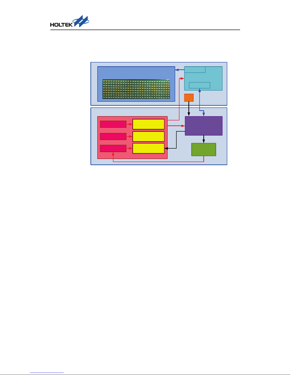
Demo H/W Block Diagram
System Block Diagram
Bottom Board
Top Board
RGB LED Matrix
(8COM x 42ROW x 2
)
HT
1635A
/B
x 2
(64LQFP)
COM/ROW
4-wire/I2C
Power Supply Circuit
AC100
V
~240
V
DC
5V
18650 Li+
Battery
DC
-DC Boost Circuit
(
SY7066)
Micro USB
AC
-
DC Converter
(
FAS
10-
5-
W
)
HT66
F
50
(28SOP)
Li+ Battery
Charger
(APL3202)
Key
x 1
Figure 1 System Block Diagram
The demo PCB is composed of two boards, a top board and a bottom board. The top
board is an RGB LED Matrix board and the bottom board is a power control board. These
two boards are connected using a pin header.
• RGB LED Matrix
Two HT1635A devices or two HT1635B devices jointly drive an RGB LED Matrix
composed of 8 commons and 28 rows.
• Power Supply Circuit
The power supply circuit provides three power supply methods, AC power (100~240VAC),
power adapter (DC5V, Micro USB interface) and a Li-battery (one 18650).
• DC-DC Boost Circuit
When only using the Li-battery to supply power, enable the DC-DC boost IC (SY7066)
which will increase the battery voltage to 5V to supply power for the host MCU and the
HT1635A/HT1635B.
• Li-Battery Charging Circuit
When using the AC power or the external power adapter to supply power, enable the
Li-battery charging management IC (APL3202) to charge the battery.
• Key Section
A touch key is used for switching the display screens.
• Host MCU Section
This demo uses the HT66F50 as the master control MCU to implement data
communication with the HT1635A/HT1635B and achieve various display functions.
Page 6

HT1635A/B Wearable Sports Bracelet LED Display Application
6 / 19 AN0393E
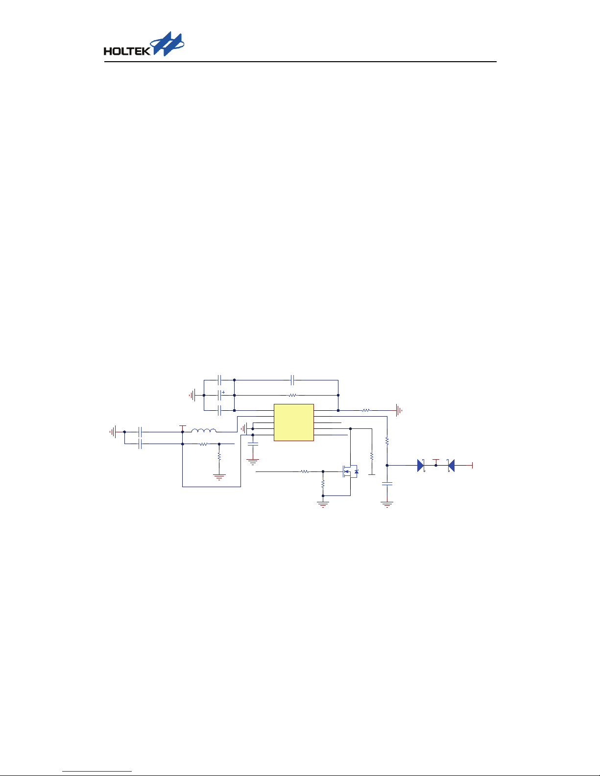
Application Circuits
Figure 2 RGB LED Matrix Circuit
The RGB LED Matrix PCB is available for the HT1635A and HT1635B. Switching
between these two devices can be achieved by using several 0Ω resistors, therefore a
general device name HT1635 is used in the schematic diagram.
Page 7

HT1635A/B Wearable Sports Bracelet LED Display Application
7 / 19 AN0393E
Figure 3 Power Control Board Circuits
Power Supply Circuits
Figure 4 AC Power and Power Adapter (Micro USB) Power Supply Circuit
Figure 5 18650 Li-battery Power Supply Circuit
VIN
4
ISET
5
STAT
1
BATT
3
GND
2
U4
APL3202-SOT23-5
VIN
2
VOUT
3
GND
1
U2
HT7125-SOT89
D2
SS54
4.7uF
C12
1KR17
3KR18
NRS6028T1R5NMGJ
L1
VCC
VDD
S1
IO_BAT1_CHGEN
0.1uF
C3
1000uF/25V
C2
ADC_VREF
10K
R2
2K
R1
10nF
C4
IO_ACIN
0.1uF
C13
10uF
C14
D7
LED
D1
TVS/SMAJ6.0CA
1
2
J1
AC 2DIP SOCKET
F1 1A fuse
Z1
ZNR
0.1uF/275VAC
C1
MCU_VDD
100K
R21
0.1uF
C17
ADC_VREF
RESET_KEY
PA0/C0X/TP0_0/AN0
1
VSS/AVSS
2
PB4/XT2
3
PB3/XT1
4
PB2/OSC2
5
PB1/OSC1
6
VDD
7
PB0/RES
8
PC1/TP1B_1/SCOM1
9
PC0/TP1B_0/SCOM0
10
PC7/[TP1A]/SCOM3
11
PC6/[TP0_0]/SCOM2
12
PD3/[TCK1]/TP3_0/[SDO]
13
PD2/[TCK0]/[SDI/SDA]
14
PD1/[TP2_0]/[SDO]/[SCK/SCL]
15
PD0/[TCK2]/TP3_1/[SCS]
16
PC5/[INT1]/TP0_1/TP1B_2/[PCK]
17
PC4/[INT0]/[PINT]/TCK3/TP2_1
18
PC3/PINT/TP2_0/C1-
19
PC2/TCK2/PCK/C1+
20
PB5/SCS/VREF
21
PA7/SCK/SCL/AN7
22
PA6/SDI/SDA/AN6
23
PA5/C1X/SDO/AN5
24
PA4/INT1/TCK1/AN4
25
PA3/INT0/C0-/AN3
26
PA2/TCK0/C0+/AN2
27
PA1/TP1A/AN1
28
U5 HT66F50-28SOP-A
0RR6
0RR5
MCU_VDD
VDD1
0R/0805R7
VDD2
0.1uF
C15
MCU_VDD
0.1uF
C18
100K
R15
100K
R16
1nF
C11
AD_BAT1V
VBAT
10K
R19
10R
R20
KEY
CSB1
RDB
WRB
DATA
CSB2
ICPDA
ICPCK
RST
AD_BAT1V
IO_ACIN
IO_BAT1_CHGEN
L
3
N
2
V-
4
V+
5
FG
1
U1
FAS10-5-W
MCU_VDD
NC
C16
220RR25
300RR22
D8
1N4148
FB/471R26
330RR27
330RR28
330RR29
MCU_VDD
RST
ICPCK
ICPDA
1
2
J3
Li+ BAT/3.7V Battery Box
1
2
3
4
5
J4
0RR33
IO_BOOSTEN
NC
R31
NC
R32
MCU_VDD
WRB
DATA
NCR24
330RR30
750KR13
0R/0805R7'
IO_CHG_DET
IO_CHG_DET
0RR23
1
2
3
4
5
MICRO USB
D3 SS54
IO_USBIN
10K
R4
10nF
C5
2K
R3
IO_USBIN
D9
TVS/MSMP6.0A
CSB1
RDB
WRB
DATA
CSB2
KEY
1
12
2 11
3 10
4
9
5
8
6 7
J5
GND1
VDD2
VDD1
Q3
AO3400
PVOUT
1
LX
2
PGND
3
SGND
4
IN
5
SVOUT
6
EN
7
LBI
8
LBO
9
FB
10
U3
SY7066_DFN10
240KR14
300KR8
51K
R9
100KR34
22uF/10V/1206C7
22uF/10V/1206C8
22uF/10V/1206
C10
4.7uF
C22
1uF
C9
VDD
LBI
LBI
VBAT
D4
SS54
VOUT
VOUT
10K
R11
10RR10
IO_BOOSTEN
Q1
AO3400
VOUT
220uF/16V/7343
C19
VBAT
100KR12
D5
SS54
VBAT
22uF/10V/1206
C20
NCC21
22uF/10V/1206
C6
D2
SS54
VDD
VCC
0.1uF
C3
1000uF/25V
C2
10K
R2
2K
R1
10nF
C4
IO_ACIN
D1
TVS/SMAJ6.0CA
1
2
J1
AC 2DIP SOCKET
F1 1A fuse
Z1
ZNR
0.1uF/275VAC
C1
0RR6
0RR5
MCU_VDD
VDD1
0R/0805R7
VDD2
L
3
N
2
V-
4
V+
5
FG
1
U1
FAS10-5-W
0R/0805R7'
1
2
3
4
5
MICRO USB
D3 SS54
IO_USBIN
10K
R4
10nF
C5
2K
R3
D9
TVS/MSMP6.0A
22uF/10V/1206
C6
S1
100K
R15
100K
R16
1nF
C11
AD_BAT1V
VBAT
1
2
J3
Li+ BAT/3.7V Battery Box
Page 8
HT1635A/B Wearable Sports Bracelet LED Display Application
8 / 19 AN0393E
The demo supports the following three power supply methods:
• AC Power
The AC power (100~240VAC) flows through a 250V/1A fuse, then a 14D471K varistor
and a 0.1μF X2 safety capacitor and finally will be converted to a 5V/2A DC power by
an AC-DC module.
• Power Adapter
Use an external DC5V/2A power adapter to supply power via a Micro USB interface.
• Li-battery
This demo provides an 18650 Li-battery holder. When the battery power key S1 is
switched on, use a 18650 Li-battery to supply power. Since the operating voltages for
the host MCU and the HT1635A/HT1635B are set to 5V, when using the Li-battery to
supply power, the DC-DC boost circuit must be used to increase the battery voltage to
5V.
Each power type is connected with a Schottky diode SS54 to be isolated from the other
two power sources. The IO_ACIN port is used to detect whether an AC power is
connected and the IO_USBIN port is used to detect whether an external power adapter is
connected. When the MCU detects an AC power or an external power adapter, the
DC-DC boost circuit will be turned off.
DC-DC Boost Circuit
Figure 6 DC-DC Boost Circuit
When there is no AC power or external power adapter connected, the demo will use a
Li-battery to supply power. When the battery voltage is higher than 3.1V, the MCU
IO_BOOSTEN port will output a low level to enable the DC-DC boost IC SY7066, which
will increase the battery voltage to 5V and provide a 2A output current. This demo uses
SILERGY’s SY7066 for the boost IC. It has a supplied package type of QFN2×2-10, an
input voltage as low as 1.8V, an output voltage of 2.5V~5.5V which is adjustable by
changing the resistance value of R13 and R14, as well as a 6A peak current.
NRS6028T1R5NMGJ
L1
750KR13
PVOUT
1
LX
2
PGND
3
SGND
4
IN5SVOUT
6
EN
7
LBI
8
LBO
9
FB
10
U3
SY7066_DFN10
240KR14
300KR8
51K
R9
1
00
K
R
34
22uF/10V/1206C7
22uF/10V/1206C8
22uF/10V/1206
C10
4.7uF
C22
1uF
C9
VDD
LBI
LBI
VBAT
D4
SS54
VOUT
VOUT
10K
R11
10RR10
IO_BOOSTEN
Q1
AO3400
VOUT
220uF/16V/7343
C19
VBAT
1
00
K
R
12
D5
SS54
VBAT
22uF/10V/1206
C20
NCC21
Page 9

HT1635A/B Wearable Sports Bracelet LED Display Application
9 / 19 AN0393E
Li-battery Charging Circuit
Figure 7 Li-battery Charging Circuit
When the MCU detects that an AC power or an external power adapter is connected, its
IO_BAT1_CHGEN port will output a high level to enable the Li-battery power
management IC, APL3202, which will charge one 18650 Li-battery. The APL3202 used in
this demo is APNEC’s product that has a supplied package type of SOT23-5, an input
voltage of 4.35V~6.5V and a charging current of 0.1A~0.5A which is adjustable by
changing the R18 resistance value. When the battery voltage is increased to 4.2V,
charging operation stops, when the battery voltage falls to 4.05V, charging operation
restarts. The R18 resistance value is 3K and the charging current is about 300mA. When
the LED D7 is on, it indicates that the Li-battery is charging, when it is off, it indicates that
the battery power is full.
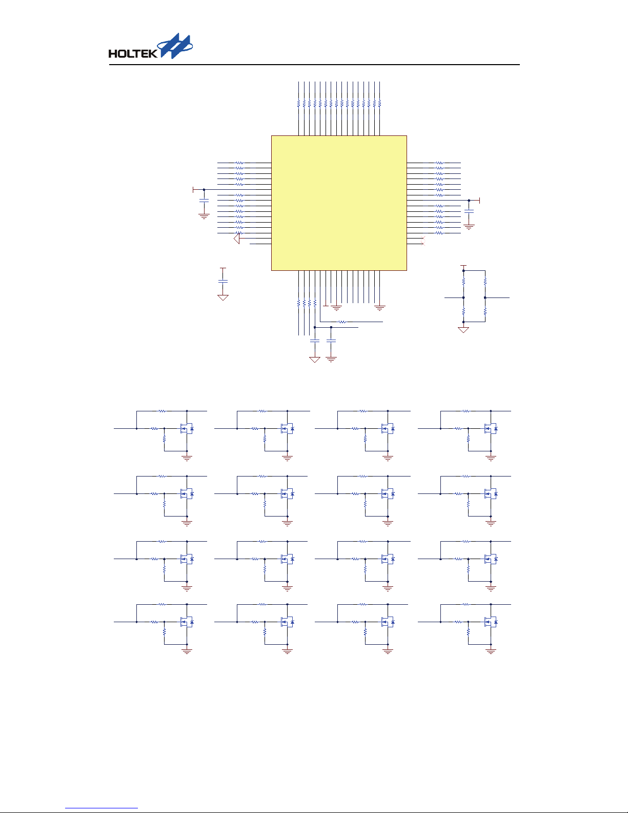
RGB LED Matrix Driving Circuit
VIN
4
ISET
5
STAT
1
BATT
3
GND
2
U4
APL3202-SOT23-5
4.7uF
C12
1KR17
3KR18
VDD
IO_BAT1_CHGEN
D7
LED
10K
R19
10R
R20
1
2
J3
Li+ BAT/3.7V Battery Box
IO_CHG_DET
Q3
AO3400
ROW12
1
ROW11
2
ROW10
3
ROW9
4
ROW8
5
LED_VDD
6
ROW7
7
ROW6
8
ROW5
9
ROW4
10
ROW3
11
ROW2
12
ROW1
13
ROW0
14
VSS
15
OSC
16
D
ATA
17
WRB18RDB
1
9
CS
B
20
S
YNC
21
VDD22CO
M0
23
LED_
VSS
2
4
COM1
2
5
CO
M2
2
6
C
OM3
27
COM
4
28
CO
M5
29
C
OM6
30
C
OM7
31
LE
D_V
SS
3
2
ROW43
33
ROW42
34
ROW41
35
ROW40
36
ROW39
37
ROW38
38
ROW37
39
ROW36
40
LED_VDD
41
ROW35
42
ROW34
43
ROW33
44
ROW32
45
ROW31
46
ROW30
47
ROW29
48
ROW
28
49
RO
W27
5
0
ROW2
6
51
RO
W25
5
2
ROW
24
53
RO
W23
54
ROW
22
5
5
R
OW2
1
56
ROW
20
57
R
OW1
9
58
RO
W18
5
9
R
OW1
7
60
RO
W16
6
1
ROW
15
62
RO
W14
63
RO
W13
64
U1 HT1635-64LQPF
C
OM2
COM
1
COM3COM4C
OM5
COM6C
OM7
COM
8
R1
G1
B1
R2
G2
B2
R3
R4
R5R6R7
R8
R
9
R10
R11
R12
R13
R14
G3
G4
G5
G6
G7
G8G9
G
10
G11
G12
G13
G14
B3
B4
B5
B6
B7
B8
B9
B10
B11
B12
B13
B14
VDD1
VDD2
OSC
SYNC
CSB1
R
DB1
R1
R2
R3
R4
R5
R6
R7
R8
R9
R10
R11
R12
R13
R
14
R15
R16
R17
R1
8
R1
9R20
R
21
R2
2
R23R2
4
R2
5
R2
6
R2
7
R28
R29
R30
R31
R32
R33
R34
R35
R36
R37
R38
R39
R40
R41
R42
VDD1
0.1uF
C1
0.1uF
C2
VDD2
0.1uF
C3
NC
R136
NC
R137
NC
R138
NC
R139
VDD1
CSB1
300RR149
NC
C12
1
00R
R
148
1nF
C15
N
C
R
150
RDB1
W
RB
D
ATA
FB
/471
R1
34
10
0R
R1
35
NC
C16
NC
C13
220pF
C14
Page 10
HT1635A/B Wearable Sports Bracelet LED Display Application
10 / 19 AN0393E
Figure 8 RGB LED Display Circuit (HT1635A/B Section)
Figure 9 RGB LED Display Circuit (COM Driving Section)
ROW12
1
ROW11
2
ROW10
3
ROW9
4
ROW8
5
LED_VDD
6
ROW7
7
ROW6
8
ROW5
9
ROW4
10
ROW3
11
ROW2
12
ROW1
13
ROW0
14
VSS
15
OSC
16
DATA17WRB
18
RDB19CSB
20
SYNC21VDD22COM023LED_VSS
24
COM125COM226COM327COM4
28
COM529COM6
30
COM731LED_VSS
32
ROW43
33
ROW42
34
ROW41
35
ROW40
36
ROW39
37
ROW38
38
ROW37
39
ROW36
40
LED_VDD
41
ROW35
42
ROW34
43
ROW33
44
ROW32
45
ROW31
46
ROW30
47
ROW29
48
ROW2849ROW27
50
ROW2651ROW25
52
ROW2453ROW2354ROW2255ROW21
56
ROW2057ROW1958ROW1859ROW17
60
ROW1661ROW15
62
ROW1463ROW13
64
U2 HT1635-64LQPF
COM10
COM9
COM11
COM12
COM13
COM14
COM15
COM16
R16
R17
R18
R19
R21
R22
R23
R24
R26
R27
R28
G16
G17
G18
G20
G21
G22
G23
G24
G26
G27
G28
B16
B17
B18
B20
B22
B23
B25
B26
B27
B28
B21
VDD1
0.1uF
C6
VDD1
OSC
SYNC
CSB2
R45
R46
R47
R48
R49
R50
R51
R52
R53
R54
R55
R56
R57
R58
R59
R60
R61
R62
R63
R64
R65
R66
R67
R68
R69
R70
R71
R72
R73
R74
R75
R76
R77
R78
R79
R80
R81
R82
R83
R84
R43
R44
VDD2
0.1uF
C7
VDD2
0.1uF
C8
RDB2
NC
R142
NC
R143
NC
R144
NC
R145
VDD1
CSB2
R25
B24
G25
R20
G19
B19
R15
G15
B15
100RR151
2KR152
NCR153
1nF
C17
RDB2
WRB
DATA
FB/471R140
220RR141
NC
C18
10RR85
1K
R86
NCR87 COM1-1
10RR88
1K
R89
NCR90 COM1-2
10RR91
1K
R92
NCR93 COM1-3
10RR94
1K
R95
NCR96 COM1-4
10RR97
1K
R98
NCR99 COM1-5
10RR100
1K
R101
NCR102 COM1-6
10RR103
1K
R104
NCR105 COM1-7
10RR106
1K
R107
NCR108 COM1-8
10RR109
1K
R110
NCR111
COM9
10RR112
1K
R113
NCR114
COM10
10RR115
1K
R116
NCR117
COM11
10RR118
1K
R119
NCR120
COM12
10RR121
1K
R122
NCR123 COM2-5
10RR124
1K
R125
NCR126 COM2-6
10RR127
1K
R128
NCR129 COM2-7
10RR130
1K
R131
NCR132 COM2-8
COM1
COM2
COM3
COM4
COM5
COM6
COM7
COM8
COM2-1
COM2-2
COM2-3
COM2-4
COM13
COM14
COM15
COM16
Q1
AO3400
Q2
AO3400
Q3
AO3400
Q4
AO3400
Q5
AO3400
Q6
AO3400
Q7
AO3400
Q8
AO3400
Q9
AO3400
Q10
AO3400
Q11
AO3400
Q13
AO3400
Q14
AO3400
Q15
AO3400
Q12
AO3400
Q16
AO3400
Page 11

HT1635A/B Wearable Sports Bracelet LED Display Application
11 / 19 AN0393E
Figure 10 Single RGB LED Driving Method
Each HT1635A or HT1635B device on the LED display board drives a 8×14 pattern RGB
LEDs (8 commons and 42 rows). Two devices combine to drive a 8×28 pattern RGB LED
matrix. This demo uses Everlight’s 19-237B RGB SMD LED, which has four pins and is a
common cathode type. A single LED size is 1.6mm×1.6mm, which is the equal to two
0603 SMD resistors. The LED-R’s V
F
is about 1.7V~2.2V, the LED-G’s and LED-B’s VF is
about 2.6~3.3V and the maximum I
F
is 25mA. In order to obtain a higher LED brightness
level, the HT1635A/HT1635B operating voltage is set to 5V, a 150Ω resistor is connected
between the ROW I/O and the LED-R anode, a 100Ω resistor is connected between the
ROW I/O and the LED-G/LED-B anode. For those LEDs that are controlled by the same
COM, their cathodes are connected together to a NMOS (AO3400) drain terminal. The
HT1635A/HT1635B COM pins are set as PMOS open-drain outputs to control the
external NMOS on/off switching to provide a stronger COM driving capacity. When all
LEDs are on, the operating current will exceed 1A. If the COM pins are set as NMOS
open-drain outputs, a high current will directly flow into the HT1635A/HT1635B, which will
generate a device over temperature condition, which could cause damaged. To avoid
unexpected damage, this driving method is not suggested.
This demo uses a COM PMOS open-drain driving method together with an external
NMOS to drive the common cathode LED matrix. Since the COM pins are set as PMOS
open-drain outputs, when writing a logic “1” to these pins, their integrated PMOS will be
on and they will output a high level (LEDVDD). When writing logic “0” to them, their
integrated PMOS will be off and they will be in the high impedance state. Usually,
connecting a pull-low resistor in parallel between the external NMOS Gate and Source
terminals can provide a dissipation path for the NMOS source charge stored during the
COM pin high level output, by which the NMOS can be turned off. The part number for all
NMOS components on the demo is AO3400. Connecting a 1K resistor in parallel between
the gate and source terminals can achieve normal NMOS on/off control.
Touch Key Detection Circuit
Figure 11 Touch Key Circuit
As shown in the above figure, if the host MCU key detection I/O’s internal pull-high resistor
is enabled, when the key is pressed, the detection I/O will be pulled-low. D1 is an ESD
protection component. This key is used to switch the RGB LED Matrix display functions.
LED-R LED-G LED-B
R1R2
R3
R1
G1
B1
10RR85
1K
R86
NCR87 COM1-1
COM1
Q1
AO3400
KEY
KEY
D1
TVS/SMAJ6.0CA
102
C11
Page 12
HT1635A/B Wearable Sports Bracelet LED Display Application
12 / 19 AN0393E
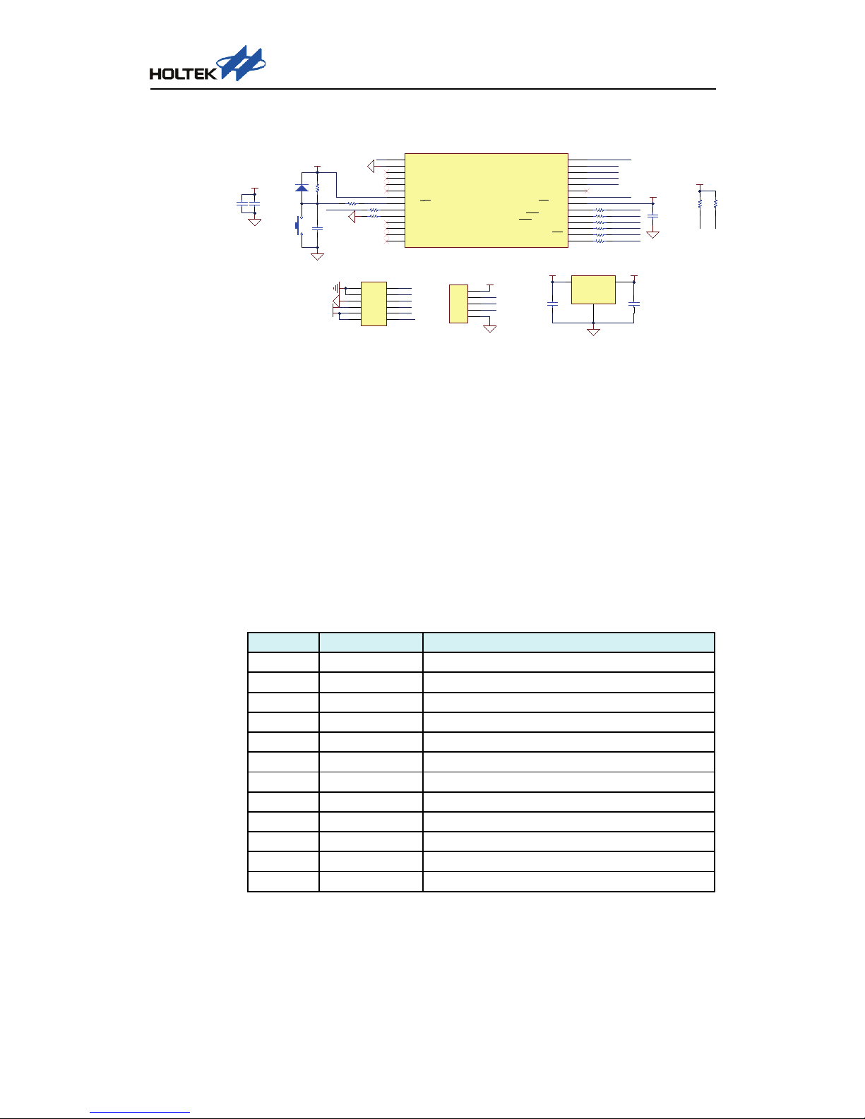
MCU Control Circuit
Figure 12 MCU Control Circuit
As the host MCU, the HT66F50 is mainly used to transfer data with the HT1635A/B via a
4-wire interface or an I
2
C interface and control the driver device to drive the RGB LED
Matrix for various display functions. In addition, the HT66F50 detects whether AC power
or an external power adapter is connected. It uses its A/D converter to sample the battery
voltage, controls the APL3202 to charge the battery or not and determines whether the
SY7066 is turned on for a battery voltage boost function. The HT66F50 has an integrated
12-bit SAR A/D converter, whose reference voltage is provided by the MCU operating
voltage being regulated to 2.5V using the HT7125. In the figure above, the pin header J5
is used for the HT1635A/HT1635B power and interface pins connection. J4 is used for the
HT66F50 In-Circuit programming pin connection.
HT66F50 I/O Control Functions:
MCU Pin Circuit Label Control Function
9 IO_CHG_DET APL3202 charging status detection
15 KEY Detects the key used for switching display functions
16 RDB 4-wire interface read serial clock
17 CSB1 4-wire interface HT1635A chip selection
18 CSB2 4-wire interface HT1635A chip selection
19 WRB I2C/4-wire interface serial clock
20 DATA I2C/4-wire interface serial data
22 IO_BOOSTEN DC-DC boost enable control
24 IO_USBIN External power adapter detection
25 IO_ACIN AC power detection
26 AD_BAT1V Li-battery voltage detection
28 IO_BAT1_CHGEN Li-battery charging enable control
VIN
2
VOUT
3
GND
1
U2
HT7125-SOT89
ADC_VREF
0.1uF
C13
10uF
C14
MCU_VDD
100K
R21
0.1uF
C17
ADC_VREF
RESET_KEY
PA0/C0X/TP0_0/AN0
1
VSS/AVSS
2
PB4/XT2
3
PB3/XT1
4
PB2/OSC2
5
PB1/OSC1
6
VDD
7
PB0/RES
8
PC1/TP1B_1/SCOM1
9
PC0/TP1B_0/SCOM0
10
PC7/[TP1A]/SCOM3
11
PC6/[TP0_0]/SCOM2
12
PD3/[TCK1]/TP3_0/[SDO]
13
PD2/[TCK0]/[SDI/SDA]
14
PD1/[TP2_0]/[SDO]/[SCK/SCL]
15
PD0/[TCK2]/TP3_1/[SCS]
16
PC5/[INT1]/TP0_1/TP1B_2/[PCK]
17
PC4/[INT0]/[PINT]/TCK3/TP2_1
18
PC3/PINT/TP2_0/C1-
19
PC2/TCK2/PCK/C1+
20
PB5/SCS/VREF
21
PA7/SCK/SCL/AN7
22
PA6/SDI/SDA/AN6
23
PA5/C1X/SDO/AN5
24
PA4/INT1/TCK1/AN4
25
PA3/INT0/C0-/AN3
26
PA2/TCK0/C0+/AN2
27
PA1/TP1A/AN1
28
U5 HT66F50-28SOP-A
0.1uF
C15
MCU_VDD
0.1uF
C18
KEY
CSB1
RDB
WRB
DATA
CSB2
ICPDA
ICPCK
RST
AD_BAT1V
IO_ACIN
IO_BAT1_CHGEN
MCU_VDD
NC
C16
220RR25
300RR22
D8
1N4148
FB/471R26
330RR27
330RR28
330RR29
MCU_VDD
RST
ICPCK
ICPDA
1
2
3
4
5
J4
IO_BOOSTEN
NC
R31
NC
R32
MCU_VDD
WRB
DATA
NCR24
330RR30
IO_CHG_DET
0RR23
IO_USBIN
CSB1
RDB
WRB
DATA
CSB2
KEY
1
12
2 11
3 10
4
9
5 8
6
7
J5
GND1
VDD2
VDD1
Page 13
HT1635A/B Wearable Sports Bracelet LED Display Application
13 / 19 AN0393E
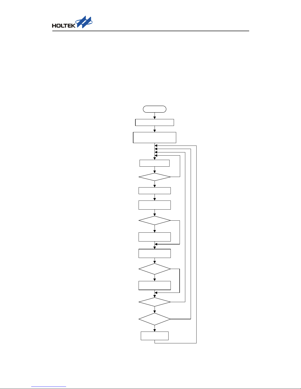
S/W Flowchart
The HT1635A/HT1635B demo board programs, written using assembly language,
include the main program, display subroutine, key scanning subroutine, power supply
detection subroutine, Li-battery power detection subroutine and timer interrupt subroutine,
etc. Owing to the different communication interfaces, there are two versions of programs
that have different data transfer methods but share the remaining subroutines. The main
program and several major subroutines will be described in the following section.
Main Program Flowchart
Start
Power supply
detection
MCU RAM and registers
and HT
1635
A
/
B initialisation
Li-
battery power
detection
Key scanning
Update system clock
Update display
TB
0F
= 1
?
1s finished ?
50
ms finished ?
CLR WDT
TB0
F =
0
Li
-battery
?
Power On Delay
100ms
Battery
Power < 3.1V ?
Y
N
Y
N
Y
Y
Y
N
N
Figure 13 Main Program Flowchart
Page 14

HT1635A/B Wearable Sports Bracelet LED Display Application
14 / 19 AN0393E
When the demo board is powered-on, the HT66F50 will implement a system initialisation,
provide a 100ms delay to ensure that the HT1635A/HT1635B internal power-on reset
circuit has enough time to complete the reset operation and then communicate with the
HT1635A/HT1635B for initial setup. In the main program loop, the host MCU firstly
detects the power supply method and then executes a key scanning, system clock update
and display update.
HT1635A/HT1635B Initialisation Flowchart
Start
COM Driving Type Setup
:
PMOS
Blinking Frequency Setup:
Blinking Off
PWM Duty Setup
:
16/16 PWM Duty
Operating Mode Setup
:
RC Master Mode0
SYS Setup:
SYS EN
LED Setup:
LED ON
Return
Figure 14 HT1635A Initialisation Flowchart (4-wire Interface)
Page 15

HT1635A/B Wearable Sports Bracelet LED Display Application
15 / 19 AN0393E
Start
HT1635B Addresses:
IC1 A1A0=11b, IC2 A1A0=10b
Blinking Frequency Setup:
Blinking Off
PWM Duty Setup: 16/16 PWM Duty
Operating Mode Setup:
RC Master Mode0
SYS & LED Setup:
SYS EN & LED ON
Return
COM Driving Type Setup: PMOS
Figure 15 HT1635B Initialisation Flowchart (I2C Interface)
Before the HT1635A/HT1635B can drive the LED Matrix, some initialisation setup should
first be executed, such as address setup (only for the HT1635B), COM driving type setup,
blinking frequency setup, PWM duty setup, operating mode setup, system setup and LED
setup, etc. After all these initialisation setups are completed, the HT1635A/HT1635B data
RAM can be written with values for the LED display.
Page 16

HT1635A/B Wearable Sports Bracelet LED Display Application
16 / 19 AN0393E
Display Subroutine Flowchart
Start
System On Mode?
Full screen white light on and blinks three times at a frequency of 0.5Hz
Welcome Mode?
Normal Display Mode?
Fuel Consumption
Display Mode?
Time Adjustment Mode?
After once scroll of HOLTEK logo and welcome characters, enter the
automatic demonstration screen. If the key is long-pressed, enter the normal
display mode.
1. Time Display Mode: display the setup time.
2. Heart Beat Mode: display the heart rate.
3. Meter Step Mode: increase one step each 0 .5s and clear to zero when
reaching ten thousand steps.
4. Connection Mode: enter the bluetooth connection screen automatically.
5. Charging Mode: enter the battery charging screen, after a full charge enter
the time display mode.
6. Gaming Mode: enter Tetris game screen automatically.
Short-press the key to switch between sub-modes. If the previous mode is
welcome mode, long-press the key to enter fuel consumption display mode. If
the previous mode is time adjustment mode, long-press the key to enter
welcome mode.
1. Fuel Consumption: switch between " FUEL" character and value screens
every 2s.
2. Time: switch between "HOURS" character and time screens every 2s.
3. Calories Consumption: switch between "CALS" character and value screens
every 2s.
4. Steps: switch between "STEPS" character and value screens every 2s.
5. Goal Completion Rate: switch between "GOAL" character and rate screens
every 2s.
Short-press the key to switch between sub-modes. Long- press the key to
enter time adjustment mode.
1. Adjust hour high digit, this digit blinks at a frequency of 1Hz.
2. Adjust hour low digit, this digit blinks at a frequency of 1Hz.
3. Adjust minute high digit, this digit blinks at a frequency of 1Hz.
4. Adjust minute low digit, this digit blinks at a frequency of 1Hz.
Short-press the key to adjust each digit value. Long-press the key to switch
between digits. After all digits have been adjusted, long-press the key to enter
normal display mode's sub-mode, time display mode.
N
N
N
N
Y
Y
Y
Return
N
Y
Y
Figure 16 Display Subroutine Flowchart
The display subroutine is used to update the RGB LED Matrix display contents. There are
five major modes, system on mode, welcome mode, normal display mode, fuel
consumption display mode and time adjustment mode. Each of the last three modes has
several sub-modes. Switching between these five major modes is achieved by a key long
press. Switching between sub-modes under a major mode or adjusting a time digit value
is achieved by a key short press.
Page 17

HT1635A/B Wearable Sports Bracelet LED Display Application
17 / 19 AN0393E
Touch Key Processing Subroutine Flowchart
Start
First long-press?
Switch to normal display mode. Under this
mode, short-press key to switch between
sub-modes.
Second
long-press?
Switch to fuel consumption display mode.
Under this mode, short-press key to switch
between sub-modes.
Third long-press?
Switch to hour high digit adjustment mode,
short-press key to adjust this digit value.
Fourth
long-press?
Switch to hour low digit adjustment mode,
short-press key to adjust this digit value.
Fifth long-press?
Switch to minute high digit adjustment
mode, short-press key to adjust this digit
value.
Sixth long-press?
Switch to minute low digit adjustment
mode, short-press key to adjust this digit
value.
Seventh
long-press?
Eighth
long-press?
Switch to welcome mode. Short-pressing
key is not valid. Long-press key to clear the
counter to zero.
Return
Switch to normal display mode. Under this
mode, short-press key to switch between
sub-modes.
N
Y
N
N
N
Y
Y
Y
N
N
N
N
Y
Y
Y
Y
Figure 17 Touch Key Processing Subroutine Flowchart
The touch key processing subroutine is used for RGB LED Matrix display mode screen
switching operations. In the time adjustment mode, a short key press is used to adjust the
digit value. A long key press is used to confirm the current digit value. In the other major
modes, a long key press is used to switch to other major modes and a short key press is
used to switch to other sub-modes of the current major mode.
Page 18

HT1635A/B Wearable Sports Bracelet LED Display Application
18 / 19 AN0393E
Power Supply Detection Subroutine Flowchart
Start
AC power connected
?
Turn off DC
-
DC
Boost function
Power adapter
connected
?
Return
Li
-
battery power supply
,
Set the related flag high
Enable Li-battery
charging
First power
-
on?
N
Y
Y
Y
N
N
Figure 18 Power Supply Detection Subroutine Flowchart
The MCU uses the IO_ACIN and IO_USBIN ports to detect an AC power connection or
an external 5V DC power adapter connection respectively. If there is no AC power or
power adapter detected, it indicates that the demo is using the Li-battery as its power
supply. If an AC power or an external power adapter is connected, the Li-battery boost
circuit will be turned off. Then, when a 1860 Li-battery is placed in the battery holder, the
battery charging function will be turned on.
Li-battery Power Detection Subroutine Flowchart
Start
Turn off DC
-DC boost circuit,
Turn off Li-battery charging
,
Clear HT1635A/B RAM data
Li
-battery power<3.1V?
Turn on DC-DC boost circuit
,
Turn off Li-battery charging
Return
Li-
battery power supply?
System On
Mode
?
Turn off
Li-
battery
charging
Battery placed?
Turn on
Li
-battery
charging
Y
N
N
Y
Y
Y
N
N
Figure 19 Li-battery Power Detection Subroutine Flowchart
When the demo uses a Li-battery as its power supply, the Li-battery power detection
subroutine is used to detect the current battery voltage. If the battery voltage is higher
than 3.1V, the DC-DC boost circuit will be turned on. If the battery voltage is lower than
3.1V, this indicates a low battery power, in which case the DC-DC boost circuit and the
LED Matrix display function will be turned off.
Page 19

HT1635A/B Wearable Sports Bracelet LED Display Application
19 / 19 AN0393E
Example Code
The demo example codes configuration options are shown below. Refer to the
attachment section for the detailed code.
;=============================================================;
;Sys Volt : 5.0V
;SysFreq: HIRC 4MHz
;WDT: By S/W Control
;WDT clock source fs: f
SYS
/4
;I/O or Reset function: RESB
;SIM Function: Disable
;LVR Function: Enable
;LVR Voltage Selection: 2.10V
;=============================================================;
Conclusions
This application note has introduced the HT1635A/HT1635B main features and used
some example code and application circuits to show how to use the HT1635A/HT1635B
LED driving functions.
Attachments
• Source Code Files
− 4-wire Interface Communication CODE
− I
2
C Interface Communication CODE
• Schematic Files
• Operating Description Files
 Loading...