

查询HT16220供应商
Features
Operating voltage: 2.7V~5.2V
·
Built-in RC oscillator
·
External 32.768kHz crystal or 32kHz
·
frequency source input
1/5 bias, 1/16 duty, frame frequency is 64Hz
·
Max. 48´16 patterns,16 commons,48 segments
·
Built-in internal resistor type bias generator
·
3-wire serial interface
·
8 kinds of time base/WDT selection
·
Time base or WDT overflow output
·
Built-in LCD display RAM
·
General Description
HT1626 is a peripheral device specially de
signed for I/O type mC used to expand the dis
play capability. The max. display segment of
the device are 768 patterns (48´16). It also sup
ports serial interface, buzzer sound, Watchdog
Timer or time base timer functions. The
HT1626 is a memory mapping and
multi-function LCD controller. The software
HT1626
RAM Mapping 48´16 LCD Controller for I/O mC
R/W address auto increment
·
Two selection buzzer frequencies
·
(2kHz/4kHz)
Power down command reduces power
·
consumption
Software configuration feature
·
Data mode and Command mode instructions
·
Three data accessing modes
·
VLCD pin to adjust LCD operating voltage
·
Cascade application
·
configuration feature of the HT1626 make it
suitable for multiple LCD applications includ
ing LCD modules and display subsystems. Only
three lines are required for the interface be
tween the host controller and the HT1626. The
HT162X series have many kinds of products
that match various applications.
-
-
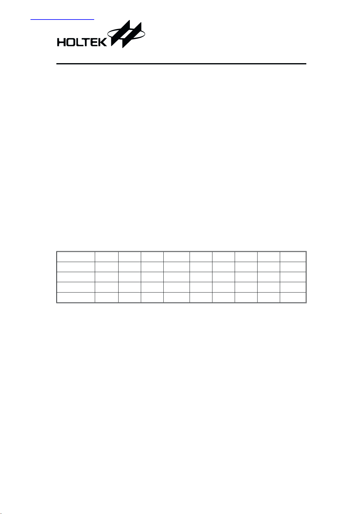
Selection Table
HT162X HT1620 HT1621 HT1622 HT16220 HT1623 HT1625 HT1626 HT1627 HT16270
COM 448 8 88
SEG 32 32 32 32 48 64
Built-in Osc.
Crystal Osc.
ÖÖ Ö ÖÖÖ Ö
ÖÖ ÖÖÖ Ö
1 April 21, 2000
16
48
16 16
64 64
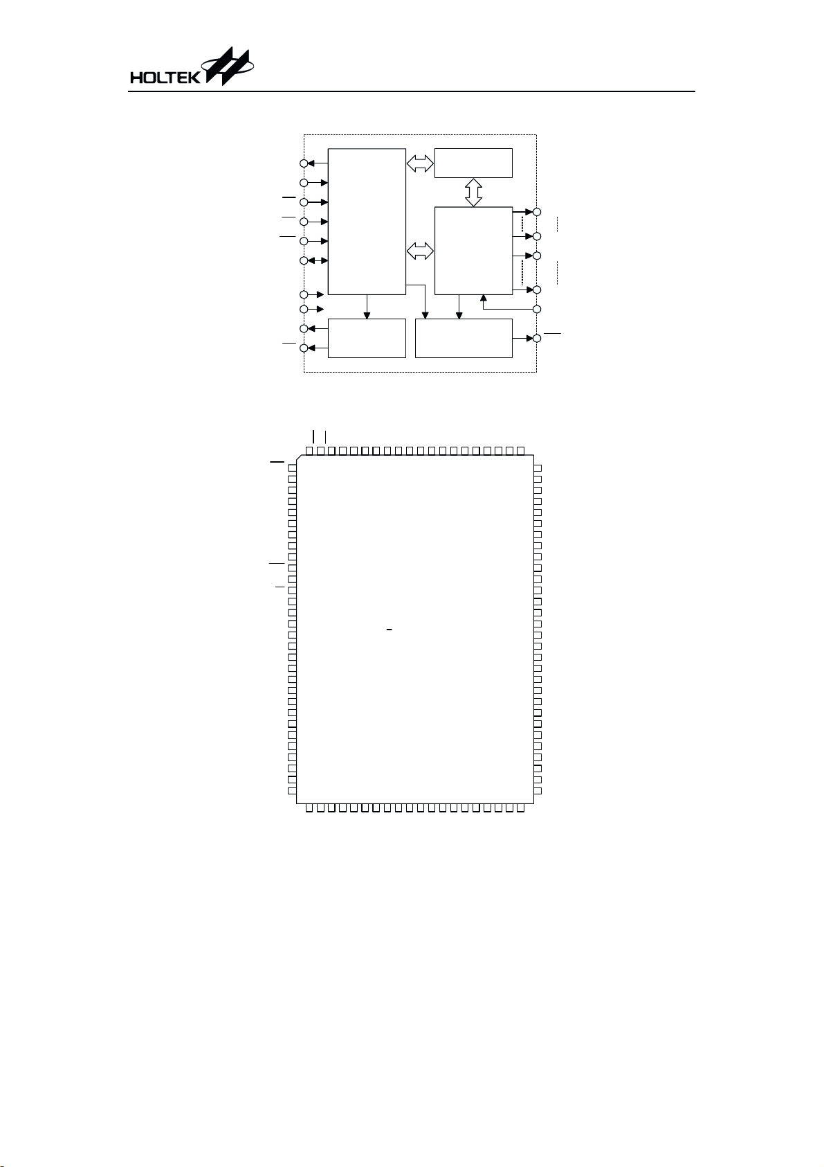
Block Diagram
HT1626
Pin Assignment
OSCO
OSCI
DATA
VDD
WR
DATA
NC
NC
VSS
OSCI
OSCO
VDD
VLCD
IR Q
BZ
BZ
T1
T2
T3
T4
COM 0
COM 1
COM 2
COM 3
COM 4
NC
COM 5
COM 6
COM 7
COM 8
COM 9
COM 10
COM 11
COM 12
CS
RD
WR
C ontrol
and
Tim ing
Circuit
VSS
BZ
BZ
Tone Frequency
G enerator
SEG 42
SEG 47
RD
CS
1
2
3
4
5
6
7
8
9
10
11
12
13
14
15
16
17
18
19
20
21
22
23
24
25
26
27
28
29
30
31
32 33 34 35 36 37 38 39 40 41 42 43 4445 46 4748 49 50
COM 13
COM 14
COM 15
SEG 43
SEG 46
SEG 45
SEG 44
SEG 2
SEG 0
SEG 1
SEG 3
SEG 4
W atchdog Tim er
Tim e Base G enerator
SEG 41
SEG 40
SEG 39
SEG 38
H T1626
100 Q FP
SEG 6
SEG 5
SEG 7
SEG 8
D ispla y R A M
LCD Driver/
Bias Circuit
and
SEG 37
SEG 36
SEG 35
SEG 10
SEG 11
SEG 9
COM 0
COM 15
SEG 0
SEG 47
VLCD
IR Q
SEG 34
SEG 33
SEG 32
SEG 31
SEG 30
81828384858687888990919293949596979899100
SEG29
80
SEG28
79
SEG27
78
SEG26
77
SEG25
76
SEG24
75
NC
74
73
NC
72
NC
71
NC
70
NC
69
NC
68
NC
67
NC
NC
66
65
NC
64
NC
63
NC
62
NC
61
NC
60
NC
59
NC
58
NC
57
SEG23
56
SEG22
55
SEG21
54
SEG20
53
SEG19
52
SEG18
51
SEG17
SEG 12
SEG 13
SEG 14
SEG 15
SEG 16
2 April 21, 2000
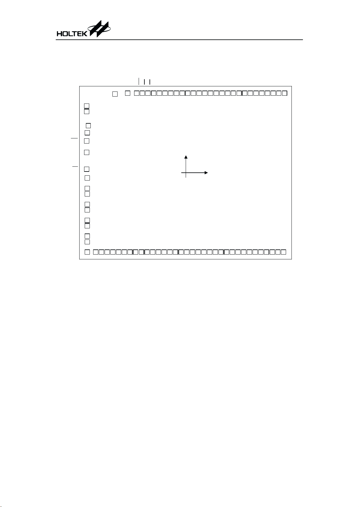
Pad Assignment
HT1626
SEG 25
SEG 24
SEG 26
SEG 27
SEG 28
SEG 29
SEG 30
SEG 31
SEG 32
SEG 33
SEG 34
SEG 35
SEG 36
SEG 37
SEG 38
SEG 39
SEG 40
SEG 41
SEG 42
SEG 43
SEG 44
SEG 45
SEG 46
WR
RD
SEG 47
CS
DATA
VSS
OSCI
OSCO
VDD
VLCD
IR Q
BZ
BZ
T1
T2
T3
T4
COM 0
COM 1
COM 2
COM 3
COM 4
1
6
10
11
12
13
14
15
16
17
COM 5
18
COM 6
19
COM 7
20
COM 8
21
COM 9
80
22
COM 10
23
COM 11
79
24
COM 12
78
25
COM 13
77
26
COM 14
27
COM 15
76
28
SEG 0
75
74
29
SEG 1
30
SEG 2
73
72
31
SEG 3
71
32
SEG 4
70
33
SEG 5
69
34
SEG 6
68
(0 , 0 )
35
SEG 7
67
36
SEG 8
66
37
SEG 9
65
38
SEG 10
64
39
SEG 11
61
62
60
63
41 2 42 3 43 4 44 5 45
40
SEG 12
SEG 13
SEG 14
SEG 15
SEG 16
59
58
SEG 17
54
55
56
57
46 7 47 8 48 9 49
SEG 18
SEG 19
SEG 20
SEG 21
53
50
SEG 22
52
51
SEG 23
Chip size: 242 ´ 196 (mil)
2
* The IC substrate should be connected to VDD in the PCB layout artwork.
3 April 21, 2000
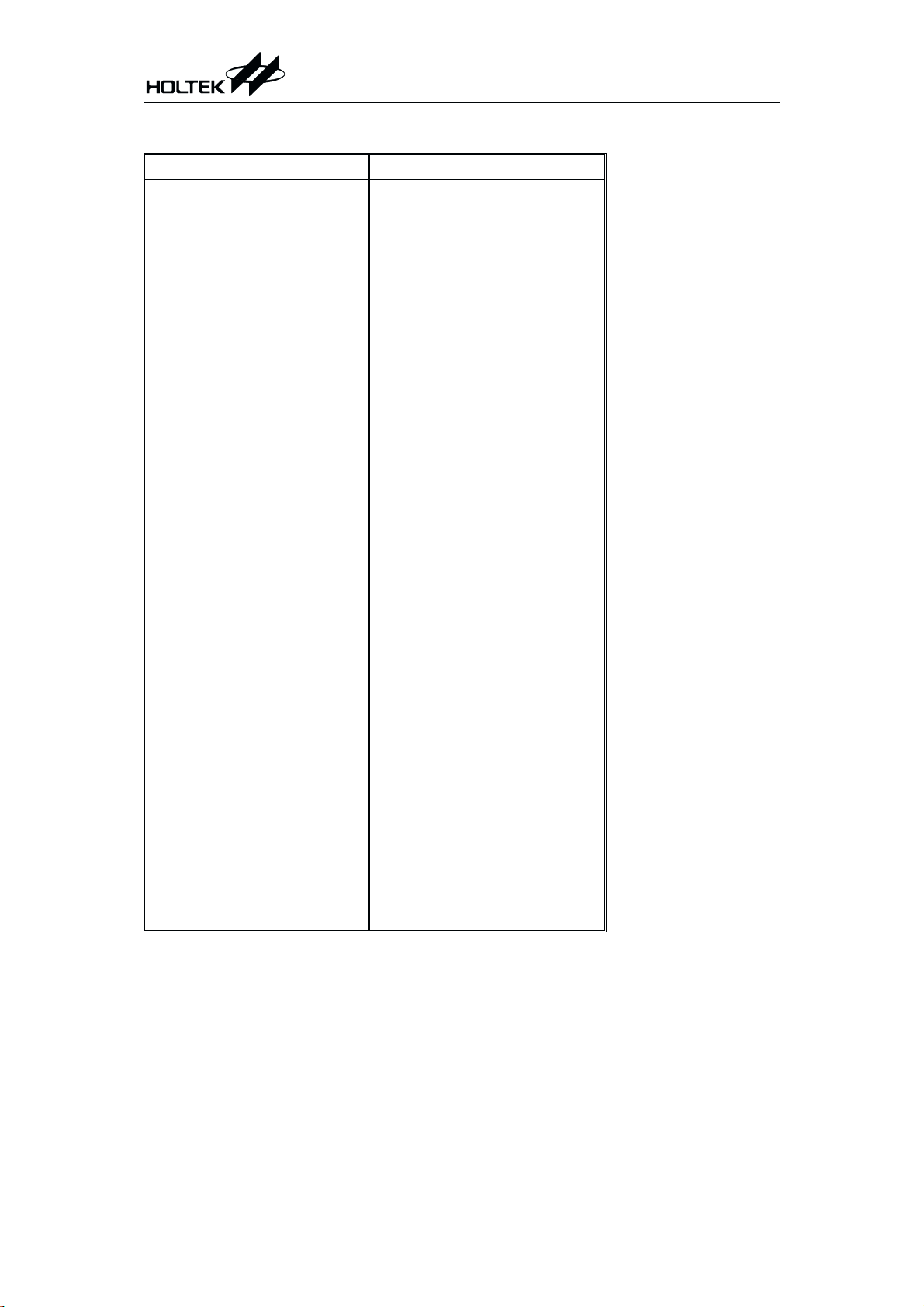
Pad Coordinates Unit: mil
Pad No. X Y Pad No. X Y
1
2
3
4
5
6
7
8
9
10
11
12
13
14
15
16
17
18
19
20
21
22
23
24
25
26
27
28
29
30
31
32
33
34 1.06
35 7.69
36 14.32
37 20.95
38 27.58
39 34.21
40 40.84
-115.68
-115.68
-113.69
-114.92
-115.68
-115.68
-115.68
-114.92 -6.29
-114.92 -18.27
-114.92 -24.91
-114.92 -36.89
-114.92 -43.52
-114.92 -55.51
-114.92 -62.13
-114.92 -74.12
-114.92 -80.75
-114.92 -92.74
-105.02 -92.74
-98.39 -92.74
-91.76 -92.74
-85.13 -92.74
-78.50 -92.74
-71.87 -92.74
-65.24 -92.74
-58.61 -92.74
-51.98 -92.74
-45.35 -92.74
-38.72 -92.74
-32.09 -92.74
-25.46 -92.74
-18.83 -92.74
-12.20 -92.74
-5.57 -92.74
77.99 41 47.47
71.36 42 54.10
54.83 43 60.73
46.62 44 67.36
37.10 45 73.99
23.80 46 80.62
4.21 47 87.25
48 93.88
49 100.51
50 107.14
51 113.77
52 114.88 92.74
53 108.25 92.74
54 101.62 92.74
55 94.99 92.74
56 88.36 92.74
57 81.73 92.74
58 75.10 92.74
59 68.47 92.74
60 61.84 92.74
61 55.21 92.74
62 48.58 92.74
63 41.95 92.74
64 35.32 92.74
65 28.69 92.74
66 22.06 92.74
67 15.43 92.74
68 8.80 92.74
69 2.17 92.74
-92.74
-92.74
-92.74
-92.74
-92.74
-92.74
-92.74
70
71
72
73
74
75
76
77
78
79
80
-4.46
-11.09
-17.72
-24.35
-30.98
-37.61
-44.24
-50.87
-57.50
-68.04
-82.71
-92.74
-92.74
-92.74
-92.74
-92.74
-92.74
-92.74
-92.74
-92.74
-92.74
-92.74
92.74
92.74
92.74
92.74
92.74
92.74
92.74
92.74
92.74
92.74
91.97
HT1626
4 April 21, 2000
Pad Description
Pad No. Pad Name I/O Description
The OSCI and OSCO pads are connected to a 32.768kHz crystal
in order to generate a system clock. If the system clock comes
1 OSCI I
2 OSCO O
3 VDD
4 VLCD I LCD operating voltage input pad.
5 IRQ
6, 7 BZ, BZ
8~11 T1~T4 I Not connected
12~27 COM0~COM15 O LCD common outputs
28~75 SEG0~SEG47 O LCD segment outputs
76 CS
77 RD
78 WR
79 DATA I/O Serial data input/output with pull-high resistor
80 VSS
from an external clock source, the external clock source should
be connected to the OSCI pad. But if an on-chip RC oscillator is
selected instead, the OSCI and OSCO pads can be left open.
Positive power supply
¾
Time base or Watchdog Timer overflow flag, NMOS open drain
O
output
O 2kHz or 4kHz tone frequency output pair
Chip selection input with pull-high resistor. When the CS
logic high, the data and command read from or write to the
HT1626 are disabled. The serial interface circuit is also reset.
I
But if the CS
data and command transmission between the host controller
and the HT1626 are all enabled.
READ clock input with pull-high resistor. Data in the RAM of
the HT1626 are clocked out on the rising edge of the RD
I
The clocked out data will appear on the data line. The host controller can use the next falling edge to latch the clocked out data.
WRITE clock input with pull-high resistor. Data on the DATA
I
line are latched into the HT1626 on the rising edge of the WR
signal.
Negative power supply, Ground
¾
is at logic low level and is input to the CS pad, the
HT1626
is
signal.
Absolute Maximum Ratings
Supply Voltage ..............................-0.3V to 5.5V
Input Voltage ................V
Note: These are stress ratings only. Stresses exceeding the range specified under ²Absolute Maxi
mum Ratings² may cause substantial damage to the device. Functional operation of this de
vice at other conditions beyond those listed in the specification is not implied and prolonged
exposure to extreme conditions may affect device reliability.
-0.3V to VDD+0.3V
SS
Storage Temperature.................-50°Cto125°C
Operating Temperature ..............-25°Cto75°C
5 April 21, 2000
-
-
HT1626
D.C. Characteristics
Symbol Parameter
V
I
DD1
I
DD2
I
DD11
I
DD22
I
STB
V
V
I
OL1
I
OH1
I
OL1
I
OH1
I
OL2
I
OH2
I
OL3
I
OH3
R
DD
IL
IH
PH
Operating Voltage
Operating Current
Operating Current
Operating Current
Operating Current
Standby Current
Input Low Voltage
Input High Voltage
BZ, BZ, IRQ
BZ, BZ
DATA
DATA
LCD Common Sink Current
LCD Common Source Current
LCD Segment Sink Current
LCD Segment Source Current
Pull-high Resistor
Test Conditions
V
DD
Conditions
¾¾
3V
No load/LCD ON
On-chip RC oscillator
5V
3V
No load/LCD ON
Crystal oscillator
5V
3V
No load/LCD OFF
On-chip RC oscillator
5V
3V
No load/LCD OFF
Crystal oscillator
5V
3V
No load
Power down mode
5V
3V
DATA, WR,CS,RD
5V 0
3V
DATA, WR,CS,RD
5V 4.0
V
3V
5V
3V
5V
3V
5V
3V
5V
3V
5V
3V
5V
3V
5V
3V
5V
3V
5V 50 100 150
=0.3V
OL
=0.5V
V
OL
V
=2.7V
OH
V
=4.5V
OH
V
=0.3V
OL
=0.5V
V
OL
V
=2.7V
OH
V
=4.5V
OH
V
=0.3V
OL
=0.5V
V
OL
V
=2.7V
OH
V
=4.5V
OH
V
=0.3V
OL
=0.5V
V
OL
V
=2.7V
OH
V
=4.5V
OH
DATA, WR,CS,RD
Min. Typ. Max. Unit
2.7
¾
155 310
¾
260 420
¾
150 310
¾
250 420
¾
830
¾
20 60
¾
¾¾
¾¾
112
¾
224
¾
0
¾
¾
2.4
¾
¾
0.9 1.8
1.7 3
-0.9 -1.8 ¾
-1.7 -3 ¾
0.9 1.8
1.7 3
-0.9 -1.8 ¾
-1.7 -3 ¾
80 160
180 360
-40 -80 ¾mA
-90 -180 ¾mA
50 100
120 240
-30 -60 ¾mA
-70 -140 ¾mA
100 200 300
Ta=25°C
5.2 V
mA
mA
mA
mA
mA
mA
20
mA
35
mA
mA
mA
0.6 V
1.0 V
3V
5V
mA
¾
mA
¾
mA
mA
mA
¾
mA
¾
mA
mA
¾mA
¾mA
¾mA
¾mA
kW
kW
6 April 21, 2000

HT1626
A.C. Characteristics
Symbol Parameter
f
SYS1
f
SYS2
f
LCD1
f
LCD2
t
COM
f
CLK1
f
CLK2
t
CS
t
CLK
t
r,tf
t
su
t
h
t
su1
t
h1
System Clock 3V On-chip RC oscillator 22 32 40 kHz
System Clock
LCD Frame Frequency
LCD Frame Frequency
LCD Common Period
Serial Data Clock (WR Pin)
Serial Data Clock (RD Pin)
Serial Interface Reset Pulse
Width (Figure 3)
WR,RDInput Pulse Width
Rise/Fall Time Serial Data
Clock Width (Figure 1)
Setup Time for DATA to WR,
RD
Clock Width (Figure 2)
Hold Time for DATA to WR,
RD
Clock Width (Figure 2)
Setup Time for CS to WR,RD
Clock Width (Figure 3)
Hold Time for CS to WR,RD
Clock Width (Figure 3)
(Figure 1)
Ta=25°C
Test Conditions
Min. Typ. Max. Unit
V
DD
Conditions
5V 24 32 40 kHz
3V
¾
32
¾
kHz
External clock source
5V
3V
¾
32
¾
kHz
44 64 80 Hz
On-chip RC oscillator
5V 48 64 80 Hz
3V
¾
64
¾
External clock source
5V
n: Number of COM
¾
3V
64
¾
n/f
¾
LCD
¾¾
¾
sec
¾
150 kHz
Duty cycle 50%
5V
3V
¾¾
¾¾
300 kHz
75 kHz
Duty cycle 50%
5V
CS
¾
Write mode 3.34
¾¾
¾
150 kHz
250
¾
¾¾
3V
Read mode 6.67
Write mode 1.67
¾¾
¾¾
5V
Read mode 3.34
¾¾
3V
¾¾
120
¾
5V
3V
¾¾
120
¾
5V
3V
¾¾
120
¾
5V
3V
¾¾
100
¾
5V
3V
¾¾
100
¾
5V
Hz
Hz
ns
ms
ms
ns
ns
ns
ns
ns
7 April 21, 2000
HT1626
D
W R , R D
Clock
90%
50%
10%
t
f
t
CLK
t
r
t
CLK
Figure 1
t
CS
CS
W R , R D
Clock
50%
FIR ST
Clock
50%
t
LAS T
Clock
h1
t
su1
Figure 3
Functional Description
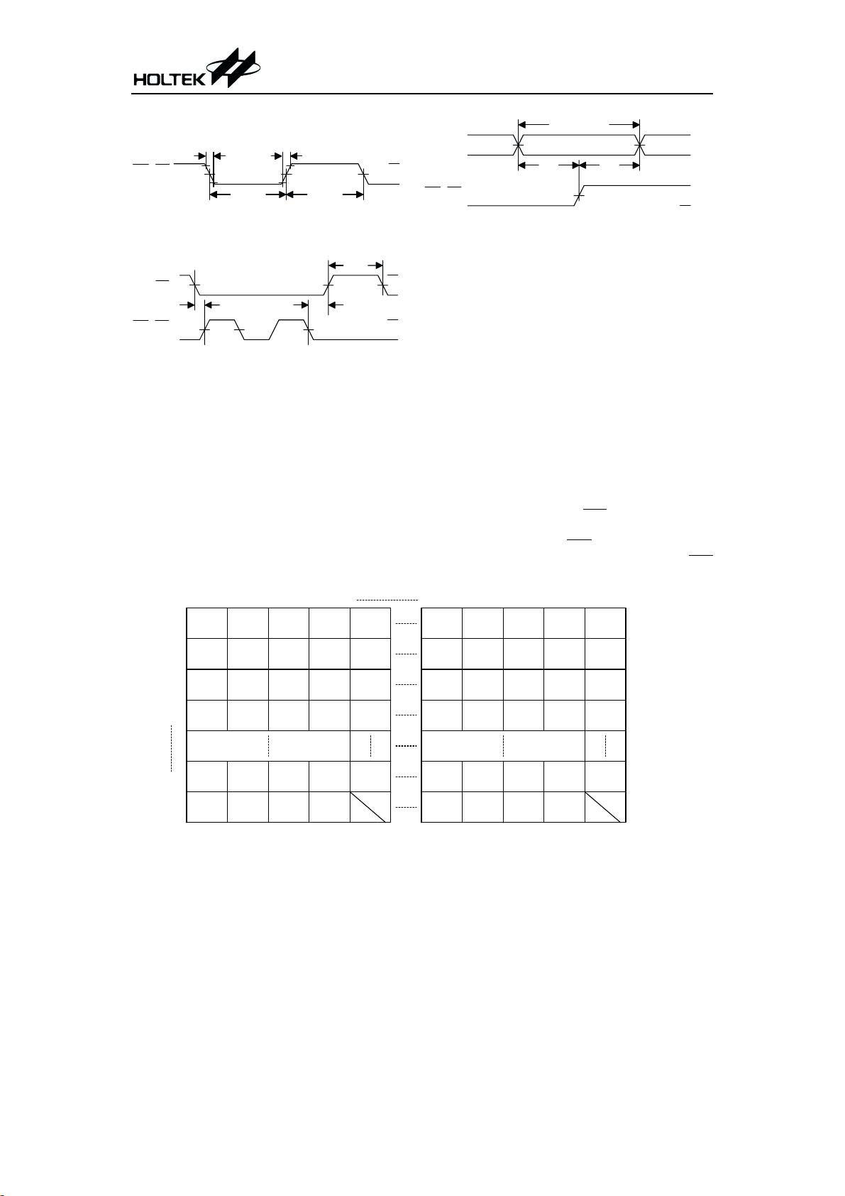
Display memory - RAM structure
The static display RAM is organized into 192´4
bits and stores the display data. The contents of
the RAM are directly mapped to the contents of
the LCD driver. Data in the RAM can be accessed by the READ, WRITE and READ-MODIFY-WRITE commands. The following is a mapping from the RAM to the LCD patterns.
COM 12COM 13COM 14COM 15
VALID DATA
V
GN
DB
DD
W R , R D
Clock
50%
50%
t
h
t
su
Figure 2
V
DD
GND
V
DD
GND
Time base and Watchdog Timer - WDT
The time base generator and WDT share the
same divided (/256) counter. TIMER DIS/EN/CLR
, WDT DIS/EN/CLR and IRQ
EN/DIS are independent from each other. Once the WDT
time-out occurs, the IRQ
pin will remain at
logic low level until the CLR WDT or the IRQ
DIS command is issued.
COM 0COM 1COM 2COM 3
V
DD
GND
V
DD
GND
SEG 0
SEG 1
SEG 2
SEG 3
SEG 47
D3 D2 D1 D0
3
7
11
15
191
Addr
Data
Data 4 Bits
(D 3, D 2, D 1, D 0)
RAM mapping
0
4
8
Address 8 B its
12
(A 7 , A 6 , ...., A 0 )
188
D3 D2 D1 D0
Addr
Data
8 April 21, 2000

HT1626
Tim e Base
C lock S ource
/256
CLR Timer
WDT
/4
CLR W DT
Timer and WDT configurations
If an external clock is selected as the source of
system frequency, the SYS DIS command turns
out invalid and the power down mode fails to be
carried out until the external clock source is re
moved.
Buzzer tone output
A simple tone generator is implemented in the
HT1626. The tone generator can output a pair
of differential driving signals on the BZ and BZ
which are used to generate a single tone.
Command format
The HT1626 can be configured by the software
setting. There are two mode commands to configure the HT1626 resource and to transfer the
LCD display data.
T IM E R E N /D IS
W D T E N /D IS
V
DD
D
CK
Q
IR Q E N /D IS
R
IR Q
The following are the data mode ID and the
command mode ID:
-
Operation Mode ID
READ Data 1 1 0
WRITE Data 1 0 1
READ-MODIFY-WRITE Data 1 0 1
COMMAND Command 1 0 0
If successive commands have been issued, the
command mode ID can be omitted. While the
system is operating in the non-successive command or the non-successive address data mode,
pin should be set to ²1², and the previous
the CS
operation mode will be reset also. The CS
returns to ²0², a new operation mode ID should
be issued first.
pin
Name Command Code Function
TONE OFF 0000-1000-X Turn-off tone output
TONE 4K 010X-XXXX-X Turn-on tone output, tone frequency is 4kHz
TONE 2K 0110-XXXX-X Turn-on tone output, tone frequency is 2kHz
9 April 21, 2000
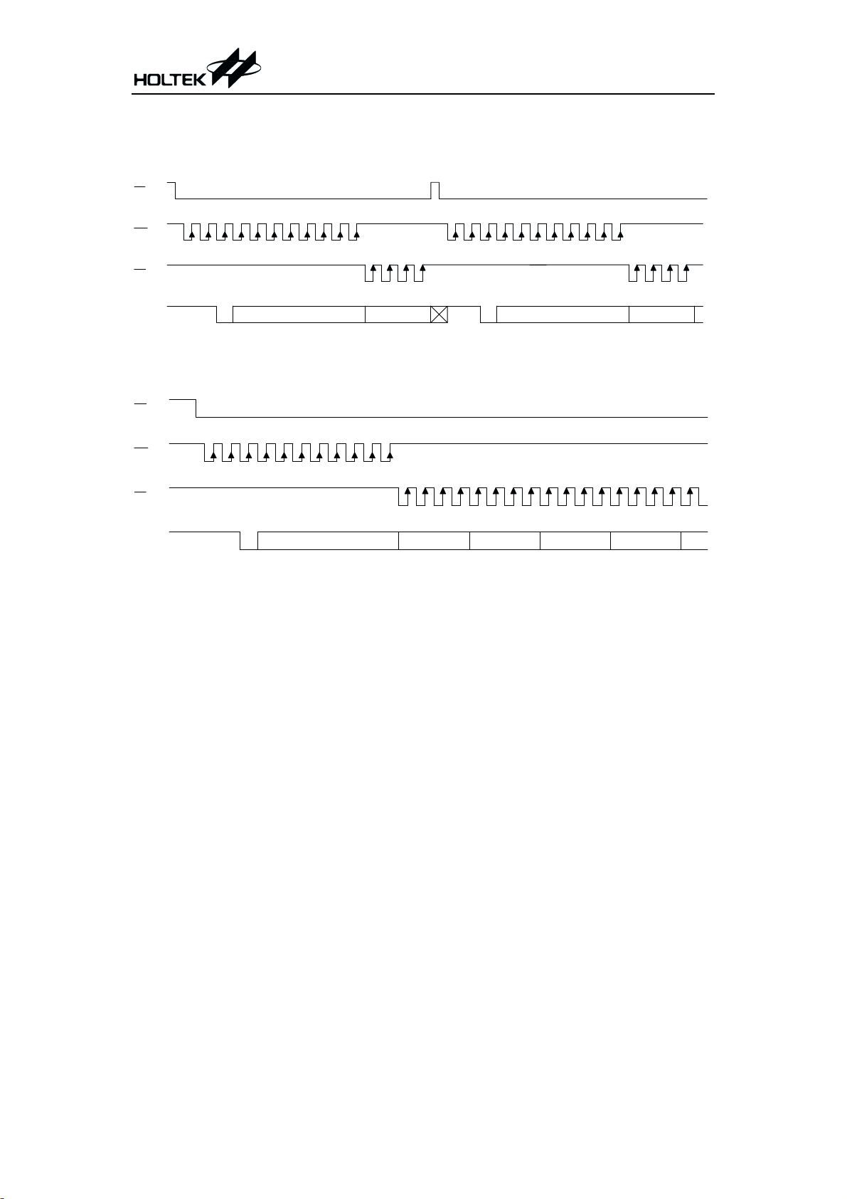
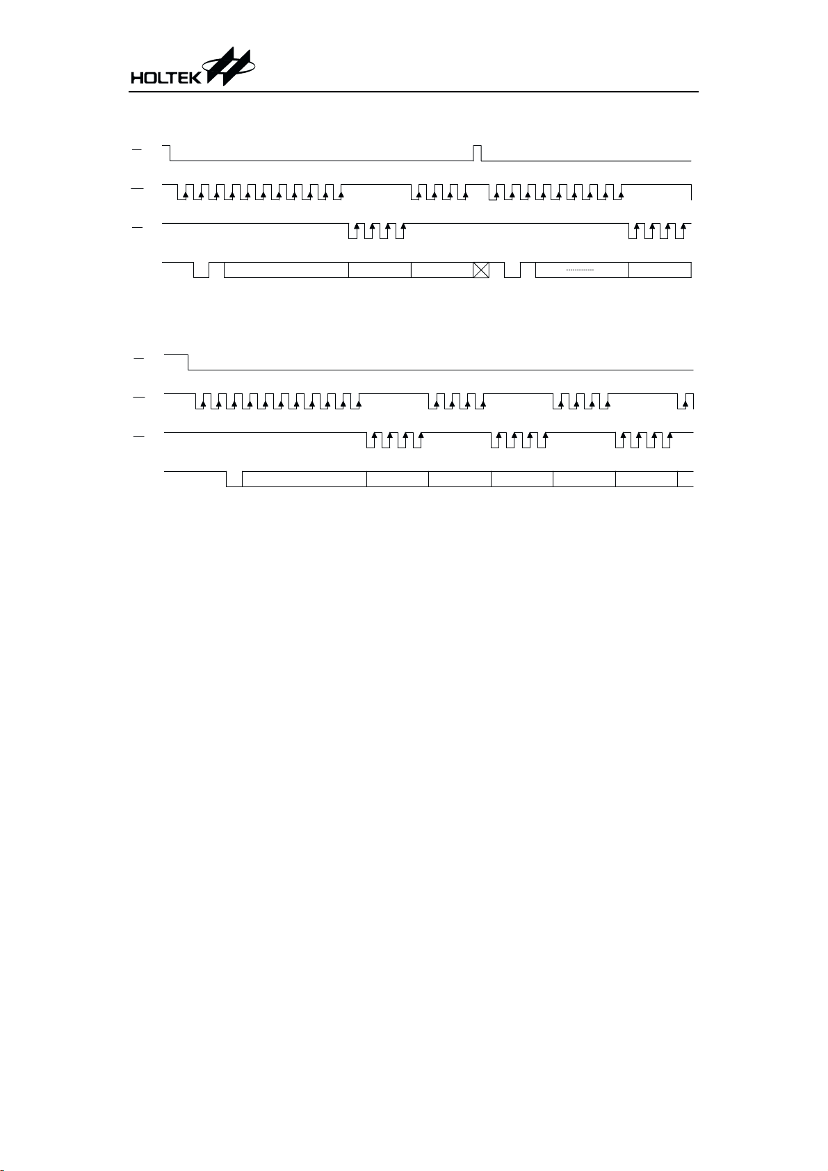
Timing Diagrams
READ mode (command code:110)
CS
WR
RD
HT1626
DATA
0A7
1
1
A5A4A3
A6 A1 A0 D 0 D1
M em ory A ddress 1 (M A 1) Data (M A2)
A2
READ mode (successive address reading)
CS
WR
RD
0
DATA
1
A7A6A5A4A3
1
M em ory A ddress (M A ) D ata (M A)
A1 A0 D 0 D1
A2
D2 D3
D ata (M A1) M em ory A ddress 2 (M A 2)
D2 D3
0
A7
A5A4A3
1
1
D0 D1
A6
D2 D3
D ata (M A+1) D ata (M A +2) D ata (M A +3)
D0 D1
A2
D2 D3
A1 A0 D0 D1
D0 D1
D2 D3
D2 D3
D0
10 April 21, 2000

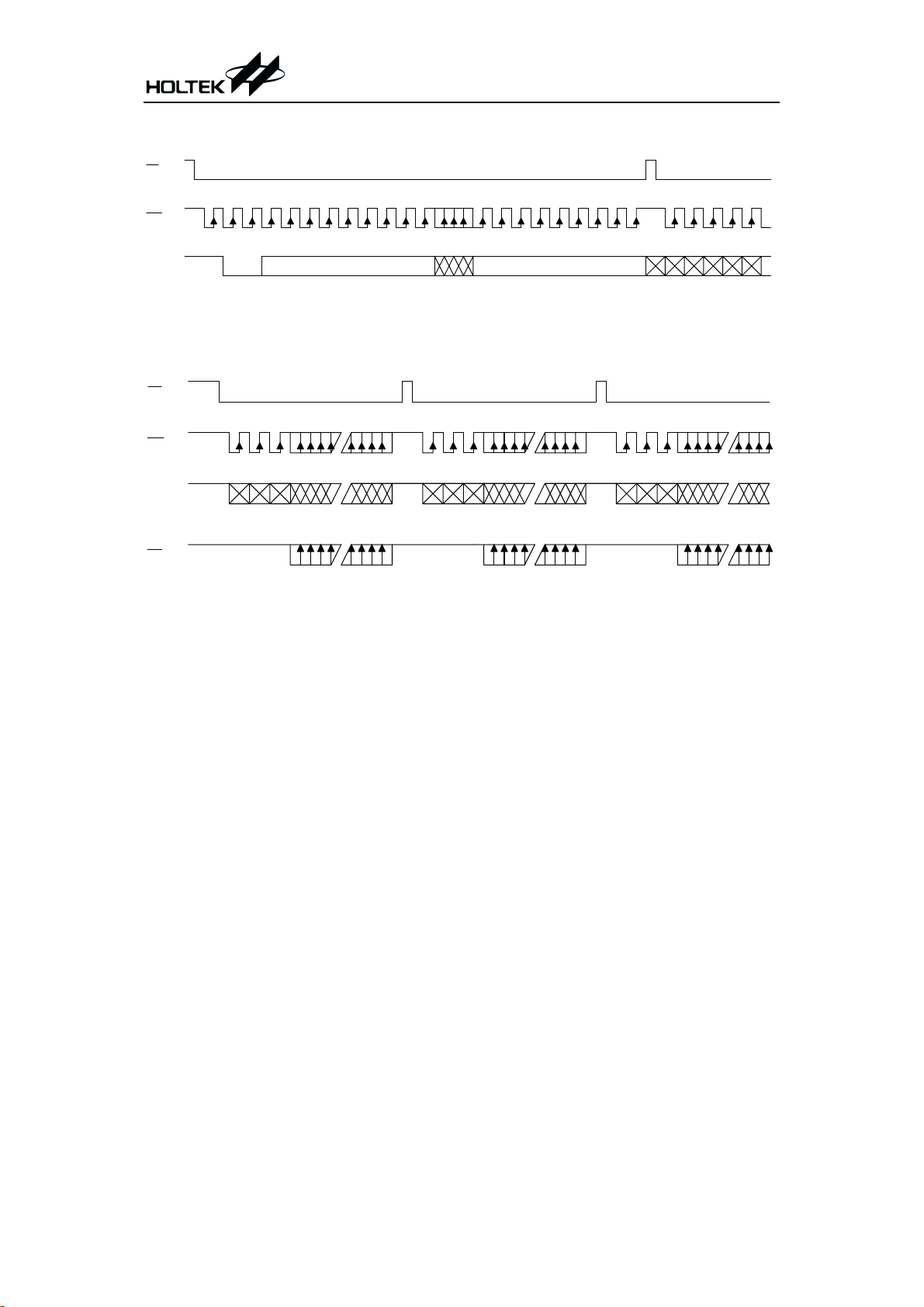
WRITE mode (command code:101)
CS
WR
HT1626
DATA
1A7
1
0
A5A4A3
A6 A1 A0 D0 D1
M em ory A ddress 1 (M A1) D ata (M A1)
A2
WRITE mode (successive address writing)
CS
WR
1
DATA
1
A7A6A5A4A3
0
M em ory A ddress (M A ) D ata (M A)
A1 A0 D0 D1
A2
D2 D3
1
A7
A5A4A3
1
0
D2 D3
D0 D1
D ata (M A+1) D ata (M A+ 2) D ata (M A+3)
A6
M em ory A ddress 2 (M A2) D ata (M A2)
D2 D3
D0 D1
A2
D2 D3
A1 A0 D 0 D1
D2 D3
D0 D1
D2 D3
D0
11 April 21, 2000
READ-MODIFY-WRITE mode (command code:101)
CS
WR
RD
HT1626
DATA
1
0
1A6
A7 A1 A0 D0 D1
A4A5A2
M em ory A ddress 1 (M A1) D ata (M A 1)
A3
D2 D3
D0 D1
Data (MA1)
D2 D3
READ-MODIFY-WRITE mode (successive address accessing)
CS
WR
RD
DATA
1
1
0
A6A7A4A5A2
M em ory A ddress (M A ) D ata (M A )
A3
A1 A0 D0 D1
D2 D3
D2 D3
D0 D1
D ata (M A) Data (M A +1) D ata (M A+1)
1
D0 D1
A6
A7
1
0
M em ory A ddress 2 (M A2) D ata (M A2)
D2 D3
D0 D1
A1 A0 D0 D1
D2 D3
D0
D1
Data (MA+2)
D2 D3
D2 D3
D0
12 April 21, 2000
Command mode (command code:100)
CS
WR
HT1626
DATA
1
0
0C8C7C6 C5
C4 C3 C2 C1
C om m and 1
Mode (data and command mode)
CS
WR
DATA
RD
C om m and
or
D ata M ode
Address and D ata
C0
C om m and
D ata M ode
C8C7C6 C5
or
C4 C3 C2 C1
C om m and iC om m and... C om m and
Address and D ata
C0
C om m and
D ata M ode
or
D ata M ode
or
Address and D ata
13 April 21, 2000

Application Circuits
m
C
C lock O ut
External C lock 1 (32kHz)
External C lock 2 (32kHz)
On-chip OSC
C rystal
32768H z
HT1626
CS
*
RD
WR
DATA
*
R
IR Q
OSCI
OSCO
C O M 0 ~ C O M 1 5 S E G 0 ~ S E G 4 7
H T1626
1/5 B ias, 1/16 D uty
LC D Panel
VDD
VLCD
BZ
BZ
*
VR
Piezo
*Note:
The connection of IRQ
The volatage applied to V
Adjust VR to fit LCD display, at V
and RD pin can be selected depending on the requirement of the mC.
pin must be lower than VDD.
LCD
DD
=5V, V
=4V, VR=15kW±20%.
LCD
Adjust R (external pull-high resistance) to fit user¢s time base clock.
14 April 21, 2000

Instruction Set Summary
Name ID Command Code D/C Function Def.
READ
WRITE
READMODIFYWRITE
SYS DIS
SYS EN
LCD OFF
LCD ON
TIMER DIS
WDT DIS
TIMER EN
WDT EN
TONE OFF
CLR TIMER
CLR WDT
RC 32K
EXT (XTAL)
32K
TONE 4K
TONE 2K
DIS
IRQ
EN
IRQ
F1
F2
F4
A7A6A5A4A3A2A1A0D0D1D2D3 D Read data from the RAM
110
A7A6A5A4A3A2A1A0D0D1D2D3 D Write data to the RAM
101
A7A6A5A4A3A2A1A0D0D1D2D3 D Read and Write data to the RAM
101
0000-0000-X C
100
0000-0001-X C Turn on system oscillator
100
0000-0010-X C Turn off LCD display Yes
100
0000-0011-X C Turn on LCD display
100
0000-0100-X C Disable time base output Yes
100
0000-0101-X C Disable WDT time-out flag output Yes
100
0000-0110-X C Enable time base output
100
0000-0111-X C Enable WDT time-out flag output
100
0000-1000-X C Turn off tone outputs Yes
100
0000-1101-X C
100
0000-1111-X C Clear the contents of the WDT stage
100
0001-10XX-X C
100
0001-11XX-X C
100
010X-XXXX-X C Tone frequency output: 4kHz
100
0110-XXXX-X C Tone frequency output: 2kHz
100
100X-0XXX-X C Disable IRQ output Yes
100
100X-1XXX-X C Enable IRQ output
100
101X-0000-X C
100
101X-0001-X C
100
101X-0010-X C
100
Turn off both system oscillator
and LCD bias generator
Clear the contents of the time
base generator
System clock source, on-chip RC
oscillator
System clock source, external
32kHz clock source or crystal
oscillator 32.768kHz
Time base clock output: 1Hz
The WDT time-out flag after: 4s
Time base clock output: 2Hz
The WDT time-out flag after: 2s
Time base clock output: 4Hz
The WDT time-out flag after: 1s
HT1626
Yes
Yes
15 April 21, 2000

Name ID Command Code D/C Function Def.
F8
F16
F32
F64
F128
TEST
NORMAL
Note:
X : Don¢t care
A7~A0 : RAM address
D3~D0 : RAM data
D/C : Data/Command mode
Def. : Power on reset denault
All the bold forms, namely 110, 101, and 100, are mode commands. Of these, 100indicates
the command mode ID. If successive commands have been issued, the command mode ID except for the first command will be omitted. The source of the tone frequency and of the time
base/WDT clock frequency can be derived from an on-chip 32kHz RC oscillator, a 32.768kHz
crystal oscillator, or an external 32kHz clock. Calculation of the frequency is based on the system frequency sources as stated above. It is recommended that the host controller should initialize the HT1626 after power on reset, for power on reset may fail, which in turn leads to the
malfunctioning of the HT1626.
101X-0011-X C
100
101X-0100-X C
100
101X-0101-X C
100
101X-0110-X C
100
101X-0111-X C
100
1110-0000-X C
100
1110-0011-X C Normal mode Yes
100
Time base clock output: 8Hz
The WDT time-out flag after: 1/2 s
Time base clock output: 16Hz
The WDT time-out flag after: 1/4 s
Time base clock output: 32Hz
The WDT time-out flag after: 1/8 s
Time base clock output: 64Hz
The WDT time-out flag after: 1/16 s
Time base clock output: 128Hz
The WDT time-out flag after: 1/32 s
Test mode, user don¢t use.
HT1626
Yes
16 April 21, 2000

HT1626
Holtek Semiconductor Inc. (Headquarters)
No.3 Creation Rd. II, Science-based Industrial Park, Hsinchu, Taiwan, R.O.C.
Tel: 886-3-563-1999
Fax: 886-3-563-1189
Holtek Semiconductor Inc. (Taipei Office)
5F, No.576, Sec.7 Chung Hsiao E. Rd., Taipei, Taiwan, R.O.C.
Tel: 886-2-2782-9635
Fax: 886-2-2782-9636
Fax: 886-2-2782-7128 (International sales hotline)
Holtek Semiconductor (Hong Kong) Ltd.
RM.711, Tower 2, Cheung Sha Wan Plaza, 833 Cheung Sha Wan Rd., Kowloon, Hong Kong
Tel: 852-2-745-8288
Fax: 852-2-742-8657
Copyright ã 2000 by HOLTEK SEMICONDUCTOR INC.
The information appearing in this Data Sheet is believed to be accurate at the time of publication. However, Holtek
assumes no responsibility arising from the use of the specifications described. The applications mentioned herein are
used solely for the purpose of illustration and Holtek makes no warranty or representation that such applications
will be suitable without further modification, nor recommends the use of its products for application that may pres
ent a risk to human life due to malfunction or otherwise. Holtek reserves the right to alter its products without prior
notification. For the most up-to-date information, please visit our web site at http://www.holtek.com.tw.
17 April 21, 2000
-
 Loading...