

RAM Mapping 32´4 LCD Controller for I/O MCU
Features
·
Operating voltage: 2.4V~5.2V
·
Built-in 256kHz RC oscillator
·
External 32.768kHz crystal or 256kHz frequency
source input
·
Selection of 1/2or1/3 bias, and selection of 1/2or
1/3or1/4 duty LCD applications
·
Internal time base frequency sources
·
Two selectable buzzer frequencies (2kHz/4kHz)
·
Power down command reduces power consumption
·
Built-in time base generator and WDT
·
Time base or WDT overflow output
·
8 kinds of time base/WDT clock sources
·
32´4 LCD driver
General Description
The HT1621 is a 128 pattern (32´4), memory mapping,
and multi-function LCD driver. The S/W configuration
feature of the HT1621 makes it suitable for multiple LCD
applications including LCD modules and display sub
HT1621
·
Built-in 32´4 bit display RAM
·
3-wire serial interface
·
Internal LCD driving frequency source
·
Software configuration feature
·
Data mode and command mode instructions
·
R/W address auto increment
·
Three data accessing modes
·
VLCD pin for adjusting LCD operating voltage
·
HT1621: 48-pin SSOP package
HT1621B: 48-pin DIP/SSOP/LQFP package
HT1621D: 28-pin SKDIP package
HT1621G: Gold bumped chip
systems. Only three or four lines are required for the in
terface between the host controller and the HT1621.
The HT1621 contains a power down command to re
duce power consumption.
-
-
-
Selection Table
HT162X HT1620 HT1621 HT1622 HT16220 HT1623 HT1625 HT1626
COM
SEG 32 32 32 32 48 64 48
Built-in Osc.
Crystal Osc.
4 4 888816
¾Ö Ö¾ÖÖÖ
ÖÖ¾ÖÖÖÖ
Rev. 1.30 1 August 6, 2003
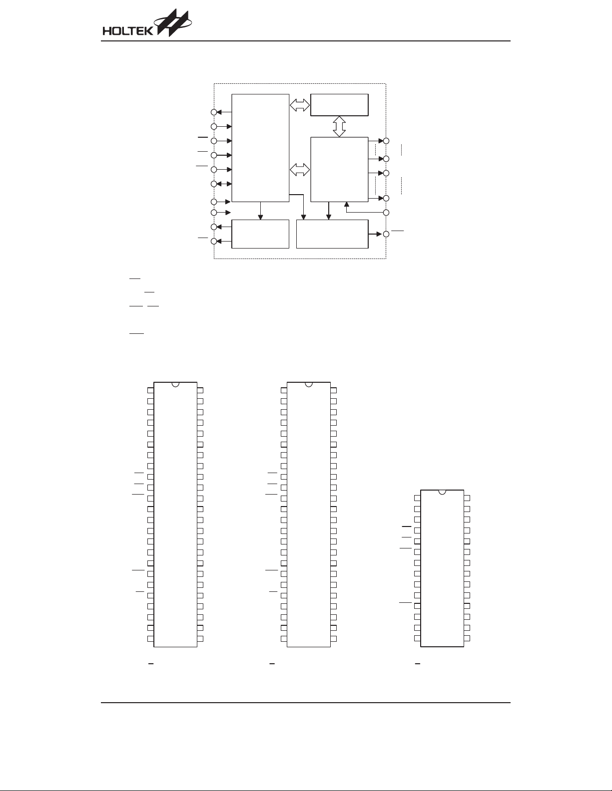
Block Diagram
HT1621
O S C O
O S C I
C S
R D
W R
D A T A
V D D
V S S
B Z
B Z
Note: CS: Chip selection
: Tone outputs
BZ, BZ
,RD, DATA: Serial interface
WR
COM0~COM3, SEG0~SEG31: LCD outputs
: Time base or WDT overflow output
IRQ
Pin Assignment
S E G 7
S E G 6
S E G 5
S E G 4
S E G 3
S E G 2
S E G 1
S E G 0
D A T A
V S S
O S C O
O S C I
V D D / V L C D
C O M 0
C O M 1
C O M 2
C O M 3
C S
R D
W R
N C
I R Q
B Z
B Z
4 8 S S O P - A
1
2
3
4
5
6
7
8
9
1 0
1 1
1 2
1 3
1 4
1 5
1 6
1 7
1 8
1 9
2 0
2 1
2 2
2 3
2 4
H T 1 6 2 1
4 8
S E G 8
4 7
S E G 9
4 6
S E G 1 0
4 5
S E G 1 1
4 4
S E G 1 2
4 3
S E G 1 3
4 2
S E G 1 4
4 1
S E G 1 5
4 0
S E G 1 6
3 9
S E G 1 7
3 8
S E G 1 8
3 7
S E G 1 9
3 6
S E G 2 0
3 5
S E G 2 1
3 4
S E G 2 2
3 3
S E G 2 3
3 2
S E G 2 4
3 1
S E G 2 5
3 0
S E G 2 6
2 9
S E G 2 7
2 8
S E G 2 8
2 7
S E G 2 9
2 6
S E G 3 0
2 5
S E G 3 1
C o n t r o l
a n d
T i m i n g
C i r c u i t
T o n e F r e q u e n c y
G e n e r a t o r
S E G 7
S E G 6
S E G 5
S E G 4
S E G 3
S E G 2
S E G 1
S E G 0
C S
R D
W R
D A T A
V S S
O S C O
O S C I
V L C D
V D D
I R Q
B Z
B Z
C O M 0
C O M 1
C O M 2
C O M 3
4 8 S S O P - A / D I P - A
D i s p l a y R A M
L C D D r i v e r /
B i a s C i r c u i t
W a t c h d o g T i m e r
a n d
T i m e B a s e G e n e r a t o r
1
2
3
4
5
6
7
8
9
1 0
1 1
1 2
1 3
1 4
1 5
1 6
1 7
1 8
1 9
2 0
2 1
2 2
2 3
2 4
4 8
4 7
4 6
4 5
4 4
4 3
4 2
4 1
4 0
3 9
3 8
3 7
3 6
3 5
3 4
3 3
3 2
3 1
3 0
2 9
2 8
2 7
2 6
2 5
H T 1 6 2 1 B
S E G 8
S E G 9
S E G 1 0
S E G 1 1
S E G 1 2
S E G 1 3
S E G 1 4
S E G 1 5
S E G 1 6
S E G 1 7
S E G 1 8
S E G 1 9
S E G 2 0
S E G 2 1
S E G 2 2
S E G 2 3
S E G 2 4
S E G 2 5
S E G 2 6
S E G 2 7
S E G 2 8
S E G 2 9
S E G 3 0
S E G 3 1
C O M 0
C O M 3
S E G 0
S E G 3 1
V L C D
I R Q
S E G 5
S E G 3
S E G 1
C S
R D
W R
D A T A
V S S
V L C D
V D D
I R Q
B Z
C O M 0
C O M 1
1
2
3
4
5
6
7
8
9
1 0
1 1
1 2
1 3
1 4
2 8
2 7
2 6
2 5
2 4
2 3
2 2
2 1
2 0
1 9
1 8
1 7
1 6
1 5
H T 1 6 2 1 D
2 8 S K D I P - A
S E G 7
S E G 9
S E G 1 1
S E G 1 3
S E G 1 5
S E G 1 7
S E G 1 9
S E G 2 1
S E G 2 3
S E G 2 5
S E G 2 7
S E G 2 9
S E G 3 1
C O M 2
Rev. 1.30 2 August 6, 2003
HT1621
S E G 1 1
S E G 1 0
S E G 9
S E G 8
S E G 7
S E G 6
S E G 5
S E G 4
S E G 3
S E G 2
S E G 1
S E G 0
Pad Assignment
S E G 0
D A T A
V S S
O S C O
O S C I
V L C D
V D D
4 64 7
4 8
1
C S
R D
2
3
W R
4
5
6
7
8
9
I R Q
1 0
1 1
B Z
B Z
1 2
S E G 2
S E G 1
1 3
C O M 0
S E G 3
1 4
1 5
C O M 2
C O M 1
S E G 4
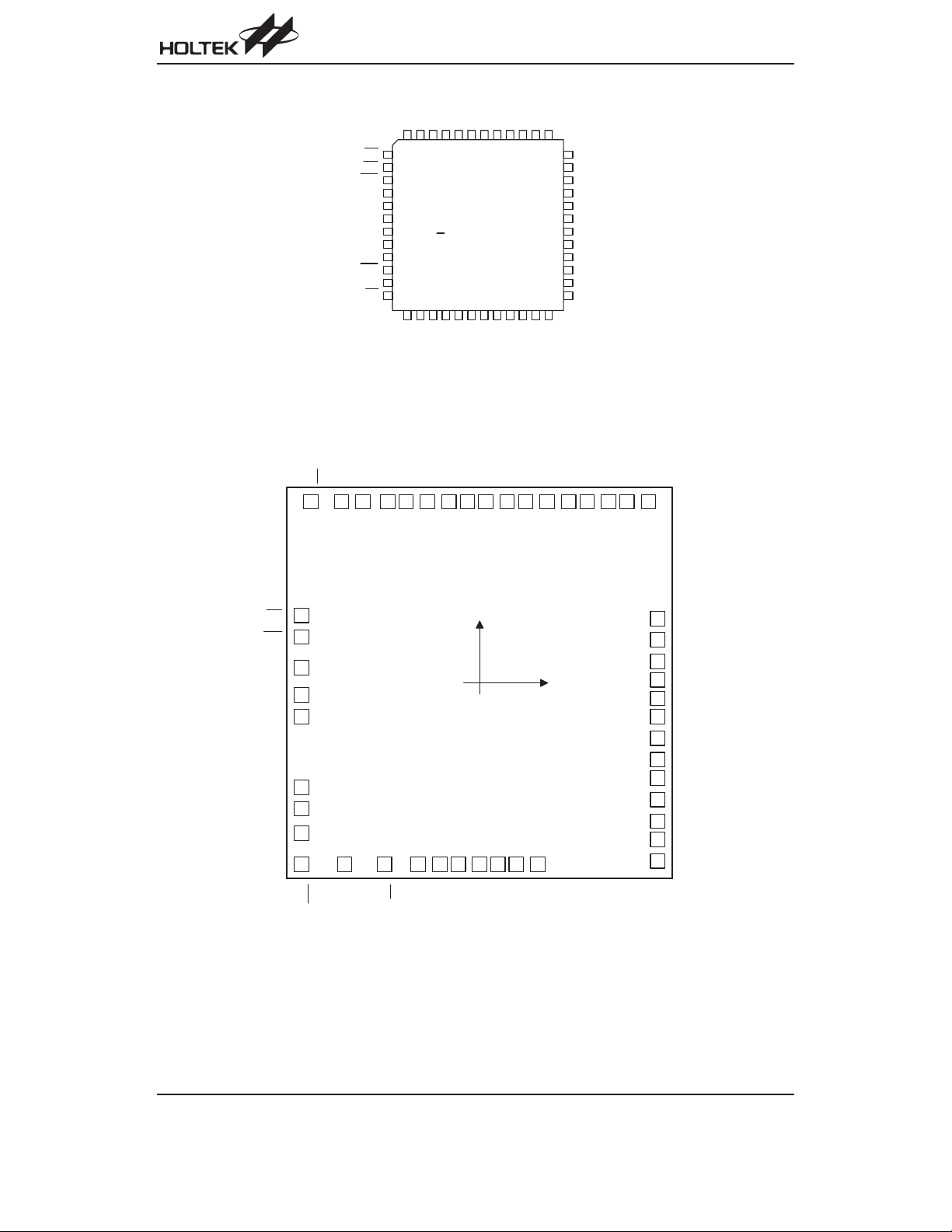
4 8 L Q F P - A
1 6
C O M 3
S E G 5
4 34 44 5
4 2
H T 1 6 2 1 B
1 8
1 7
1 9
S E G 2 9
S E G 3 0
S E G 3 1
S E G 7
S E G 6
4 1
2 0
2 1 2 2 2 3 2 4
S E G 2 8
S E G 2 7
S E G 8
3 73 83 94 0
3 6
S E G 1 2
3 5
S E G 1 3
3 4
S E G 1 4
3 3
S E G 1 5
3 2
S E G 1 6
3 1
S E G 1 7
3 0
S E G 1 8
2 9
S G E 1 9
2 8
S E G 2 0
2 7
S E G 2 1
2 6
S E G 2 2
2 5
S E G 2 3
S E G 2 4
S E G 2 5
S E G 2 6
S E G 1 5
S E G 1 4
S E G 1 3
S E G 1 2
S E G 1 1
S E G 1 0
S E G 9
C S
1
4 4
4 54 64 74 8
4 1
4 24 3
3 33 43 53 63 73 83 94 0
2
R D
3
W R
D A T A
V S S
O S C O
O S C I
V L C D
V D D
4
5
6
7
8
9
1 0
I R Q
1 2 1 3
1 1
B Z
B Z
1 4 1 5 1 6 1 7 1 8 1 9
C O M 0
C O M 1
Chip size: 127 ´ 131 (mil)
( 0 , 0 )
C O M 2
C O M 3
S E G 2 9
S E G 3 0
S E G 3 1
2
Bump height: 18mm ± 3mm
Min. Bump spacing: 72.36mm
Bump size: 96.042 ´ 96.042mm
2
* The IC substrate should be connected to VDD in the PCB layout artwork.
3 2
S E G 1 6
3 1
S E G 1 7
3 0
S E G 1 8
2 9
S E G 1 9
2 8
S E G 2 0
2 7
S E G 2 1
2 6
S E G 2 2
2 5
S E G 2 3
2 4
S E G 2 4
2 3
S E G 2 5
2 2
S E G 2 6
2 1
S E G 2 7
2 0
S E G 2 8
Rev. 1.30 3 August 6, 2003
HT1621
Pad Coordinates Unit: mil
Pad No. X Y Pad No. X Y
1
2
3
4
5
6
7
8
9
10
11
12
13
14
15
16
17 6.33
18 12.96
19 19.59
20 58.14
21 58.14
22 58.14
23 58.14
24 58.14
-55.04
-58.52
-58.52
-58.52
-58.52 -4.51
-58.52 -11.14
-58.52 -34.76
-58.52 -41.90
-58.52 -49.13
-58.52 -59.08
-44.07 -59.08
-31.58 -59.08
-20.70 -59.08
-13.98 -59.08
-7.05 -59.08
-0.34 -59.08
59.46 25 58.14
22.18 26 58.14
15.56 27 58.14
5.36 28 58.14
29 58.14 1.32
30 58.14 7.95
31 58.14 14.58
32 58.14 21.21
33 55.55 59.46
34 48.92 59.46
35 42.29 59.46
36 35.66 59.46
37 29.03 59.46
38 22.40 59.46
39 15.77 59.46
40 9.14 59.46
-59.08
-59.08
-59.08
-58.44
-51.81
-45.18
-38.55
-31.92
41 2.42 59.46
42
43
44
45
46
47
48
-4.21
-10.84
-17.47
-24.10
-30.73
-38.17
-45.39
-25.29
-18.66
-11.94
-5.31
59.46
59.46
59.46
59.46
59.46
59.46
59.46
Pad Description
Pad No. Pad Name I/O Function
Chip selection input with pull-high resistor
When the CS
1CS
2RD
3WR
4 DATA I/O Serial data input/output with pull-high resistor
5 VSS
7 OSCI I The OSCI and OSCO pads are connected to a 32.768kHz crystal in order to
6 OSCO O
8 VLCD I LCD power input
9 VDD
10 IRQ
11, 12 BZ, BZ
13~16 COM0~COM3 O LCD common outputs
48~17 SEG0~SEG31 O LCD segment outputs
the HT1621 are disabled. The serial interface circuit is also reset. But if CS
I
is at logic low level and is input to the CS pad, the data and command transmission between the host controller and the HT1621 are all enabled.
READ clock input with pull-high resistor
Data in the RAM of the HT1621 are clocked out onthe falling edge of the RD
I
signal. The clocked out data will appear on the DATA line. The host control
ler can use the next rising edge to latch the clocked out data.
WRITE clock input with pull-high resistor
I
Data on the DATA line are latched into the HT1621 on the rising edge of the
WR
signal.
Negative power supply, ground
¾
generate a system clock. If the system clock comes from an external clock
source, the external clock source should be connected to the OSCI pad. But
if an on-chip RC oscillator is selected instead, the OSCI and OSCO pads
can be left open.
Positive power supply
¾
O Time base or WDT overflow flag, NMOS open drain output
O 2kHz or 4kHz tone frequency output pair
is logic high, the data and command read from or written to
-
Rev. 1.30 4 August 6, 2003
HT1621
Absolute Maximum Ratings
Supply Voltage...........................VSS-0.3V to VSS+5.5V
Input Voltage..............................V
-0.3V to VDD+0.3V
SS
Storage Temperature ............................-50
Operating Temperature...........................-25
Note: These are stress ratings only. Stresses exceeding the range specified under ²Absolute Maximum Ratings² may
cause substantial damage to the device. Functional operation of this device at other conditions beyond those
listed in the specification is not implied and prolonged exposure to extreme conditions may affect device reliabil
ity.
o
Cto125oC
o
Cto75oC
-
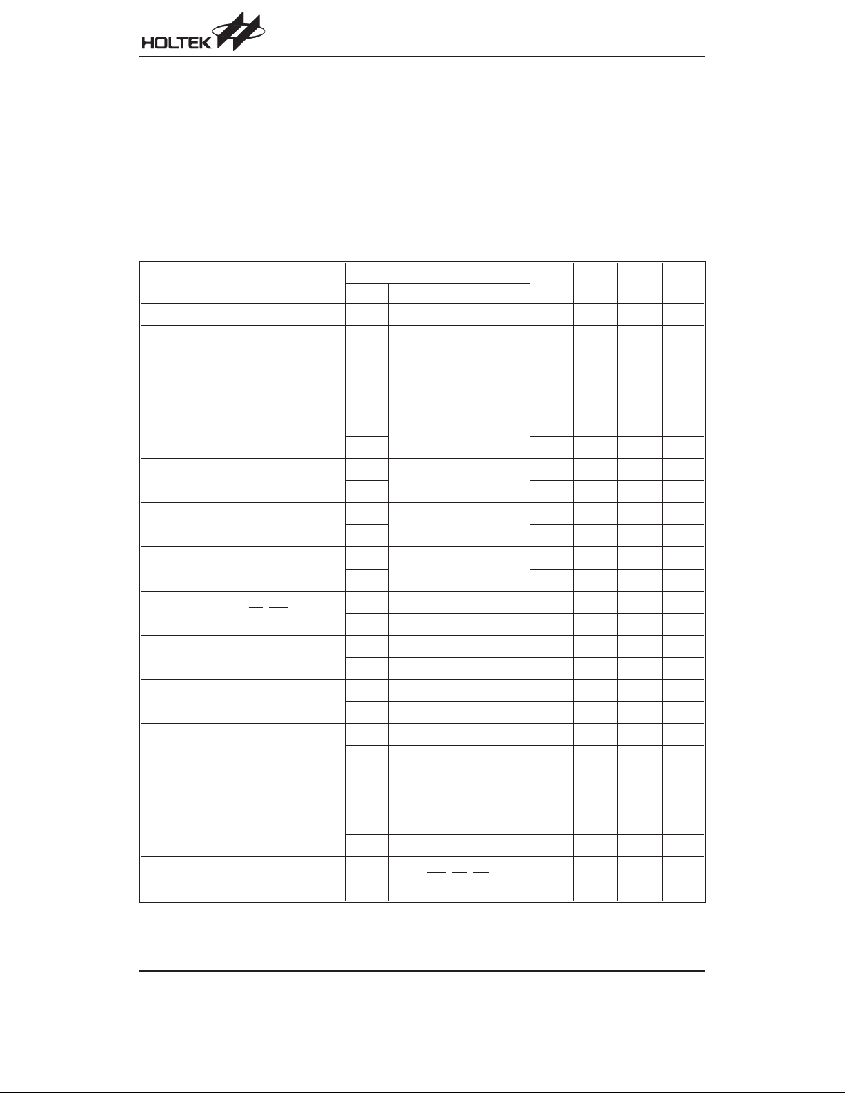
D.C. Characteristics
Symbol Parameter
V
Operating Voltage
DD
I
Operating Current
DD1
I
Operating Current
DD2
I
Operating Current
DD3
I
Standby Current
STB
V
Input Low Voltage
IL
V
Input High Voltage
IH
I
DATA, BZ, BZ, IRQ
OL1
I
DATA, BZ, BZ
OH1
I
LCD Common Sink Current
OL2
I
LCD Common Source Current
OH2
I
LCD Segment Sink Current
OL3
I
LCD Segment Source Current
OH3
R
Pull-high Resistor
PH
Test Conditions
V
DD
Conditions
¾¾
3V
No load/LCD ON
On-chip RC oscillator
5V
3V
No load/LCD ON
Crystal oscillator
5V
3V
No load/LCD ON
External clock source
5V
3V
No load, Power down mode
5V
3V
DATA, WR,CS,RD
5V 0
3V
DATA, WR,CS,RD
5V 4.0
=0.3V
V
3V
OL
V
V
V
V
V
V
V
V
V
V
V
OL
OH
OH
OL
OL
OH
OH
OL
OL
OH
OH
=0.5V
=2.7V
=4.5V
=0.3V
=0.5V
=2.7V
=4.5V
=0.3V
=0.5V
=2.7V
=4.5V
5V
3V
5V
3V
5V
3V
5V
3V
5V
3V
5V
3V
Min. Typ. Max. Unit
2.4
¾
¾
¾
¾
¾
¾
¾
¾
0
2.4
¾
150 300
300 600
60 120
120 240
100 200
200 400
0.1 5
0.3 10
¾
¾
¾
¾
5.2 V
0.6 V
1.0 V
3.0 V
5.0 V
0.5 1.2
1.3 2.6
-0.4 -0.8 ¾
-0.9 -1.8 ¾
80 150
150 250
-80 -120 ¾mA
-120 -200 ¾mA
60 120
120 200
-40 -70 ¾mA
-70 -100 ¾mA
40 80 150
DATA, WR,CS,RD
5V 30 60 100
Ta=25°C
mA
mA
mA
mA
mA
mA
mA
mA
mA
¾
mA
¾
mA
mA
¾mA
¾mA
¾mA
¾mA
kW
kW
Rev. 1.30 5 August 6, 2003
HT1621
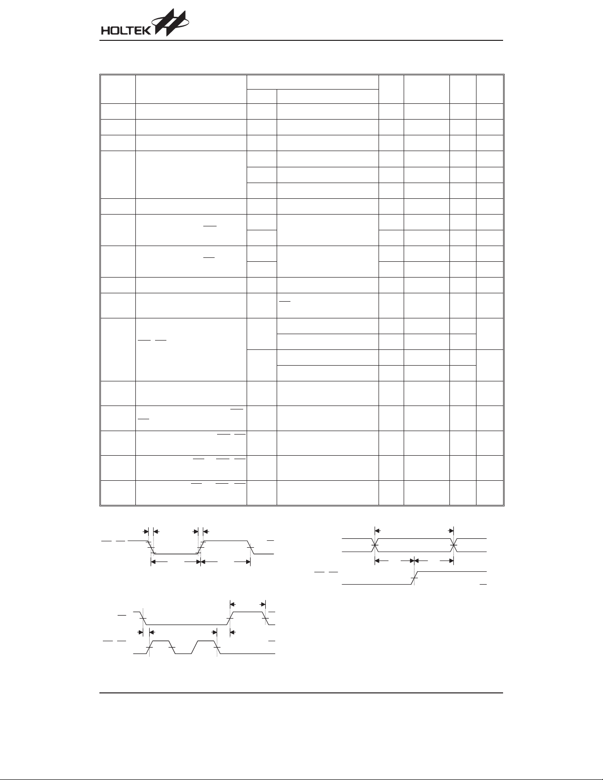
A.C. Characteristics
Symbol Parameter
f
System Clock
SYS1
f
System Clock
SYS2
f
System Clock
SYS3
f
LCD Clock
LCD
t
LCD Common Period
COM
f
Serial Data Clock (WR pin)
CLK1
f
Serial Data Clock (RD pin)
CLK2
f
Tone Frequency
TONE
Serial Interface Reset Pulse
t
CS
Width (Figure 3)
WR,RDInput Pulse Width
t
CLK
(Figure 1)
Rise/Fall Time Serial Data
t
r,tf
Clock Width (Figure 1)
Setup Time for DATA to WR,
t
su
RD
Clock Width (Figure 2)
Hold Time for DATA to WR,RD
t
h
Clock Width (Figure 2)
Setup Time for CS to WR,RD
t
su1
Clock Width (Figure 3)
Hold Time for CS to WR,RD
t
h1
Clock Width (Figure 3)
Test Conditions
V
DD
¾
¾
¾
¾
¾
¾
¾
Conditions
On-chip RC oscillator
Crystal oscillator
External clock source
On-chip RC oscillator
Crystal oscillator
External clock source
n: Number of COM
3V
Duty cycle 50%
5V
3V
Duty cycle 50%
5V
On-chip RC oscillator
¾
CS
¾
Write mode 3.34
3V
Read mode 6.67
Write mode 1.67
5V
Read mode 3.34
¾¾¾
¾¾¾
¾¾¾
¾¾¾
¾¾¾
Min. Typ. Max. Unit
32.768
f
SYS1
f
SYS2
f
SYS3
n/f
256
256
/1024
/128
/1024
LCD
¾
¾
¾
¾
¾
¾
¾
¾¾
¾¾
¾¾
¾¾
2.0 or 4.0
¾
¾
250
¾¾
¾¾
¾¾
¾¾
120
120
120
100
100
Ta=25°C
kHz
¾
kHz
¾
kHz
¾
Hz
¾
Hz
¾
Hz
¾
s
¾
150 kHz
300 kHz
75 kHz
150 kHz
kHz
¾
ns
¾
ms
ms
ns
¾
ns
¾
ns
¾
ns
¾
ns
¾
W R , R D
C l o c k
W R , R D
C l o c k
9 0 %
5 0 %
1 0 %
C S
5 0 %
F i r s t C l o c k L a s t C l o c k
t
f
t
C L K
Figure 1
t
S U 1
5 0 %
t
r
t
C L K
t
C S
t
h 1
V
G N D
V
G N D
V
G N D
D D
D D
D D
W R , R D
C l o c k
D B
5 0 %
t
S U
Figure 2
V a l i d D a t a
V
D D
t
h
5 0 %
G N D
V
G N D
D D
Figure 3
Rev. 1.30 6 August 6, 2003
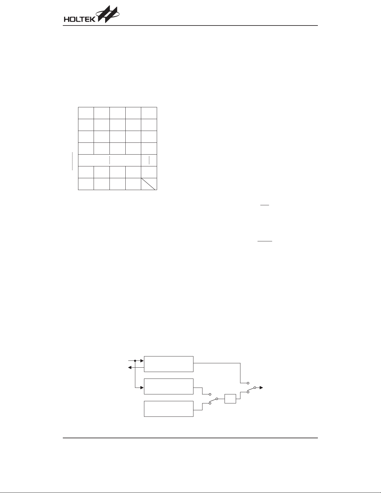
Functional Description
Display Memory - RAM
The static display memory (RAM) is organized into 32´4
bits and stores the displayed data. The contents of the
RAM are directly mapped to the contents of the LCD
driver. Data in the RAM can be accessed by the READ,
WRITE, and READ-MODIFY-WRITE commands. The
following is a mapping from the RAM tothe LCD pattern:
C O M 0C O M 1C O M 2C O M 3
S E G 0
S E G 1
S E G 2
S E G 3
S E G 3 1
D 3 D 2 D 1 D 0
D a t a 4 b i t s
( D 3 , D 2 , D 1 , D 0 )
RAM Mapping
System Oscillator
The HT1621 system clock is used to generate the time
base/Watchdog Timer (WDT) clock frequency, LCD
driving clock, and tone frequency. The source of the
clock may be from an on-chip RC oscillator (256kHz), a
crystal oscillator (32.768kHz), or an external 256kHz
clock by the S/W setting. The configuration of the system oscillator is as shown. After the SYS DIS command
is executed, the system clock will stop and the LCD bias
generator will turn off. That command is, however, avail
able only for the on-chip RC oscillator or for the crystal
oscillator. Once the system clock stops, the LCD display
will become blank, and the time base/WDT lose its func
tion as well.
The LCD OFF command is used to turn the LCD bias
generator off. After the LCD bias generator switches off
by issuing the LCD OFF command, using the SYS DIS
D a t a
0
1
2
3
3 1
A d d r
A d d r e s s 6 b i t s
( A 5 , A 4 , . . . , A 0 )
command reduces power consumption, serving as a
system power down command. But if the external clock
source is chosen as the system clock, using the SYS
DIS command can neither turn the oscillator off nor
carry out the power down mode. The crystal oscillator
option can be applied to connect an external frequency
source of 32kHz to the OSCI pin. In this case, the sys
tem fails to enter the power down mode, similar to the
case in the external 256kHz clock source operation. At
the initial system power on, the HT1621 is at the SYS
DIS state.
Time Base and Watchdog Timer (WDT)
The time base generator is comprised by an 8-stage
count-up ripple counter and is designed to generate an
accurate time base. The watch dog timer (WDT), on the
other hand, is composed of an 8-stage time base gener
ator along with a 2-stage count-up counter, and is de
signed to break the host controller or other subsystems
from abnormal states such as unknown or unwanted
jump, execution errors, etc. The WDT time-out will result
in the setting of an internal WDT time-out flag. The out
puts of the time base generator and of the WDT time-out
flag can be connected to the IRQ
output by a command
option. There are totally eight frequency sources available for the time base generator and the WDT clock.
The frequency is calculated by the following equation.
32kHz
f
=
WDT
n
2
where the value of n ranges from 0 to 7 by command options. The 32kHz in the above equation indicates that
the source of the system frequency is derived from a
crystal oscillator of 32.768kHz, an on-chip oscillator
(256kHz), or an external frequency of 256kHz.
If an on-chip oscillator (256kHz) or an external 256kHz
frequency is chosen as the source of the system fre
quency, the frequency source is by default prescaled to
32kHz by a 3-stage prescaler. Employing both the time
base generator and the WDT related commands, one
should be careful since the time base generator and
WDT share the same 8-stage counter. For example, in
voking the WDT DIS command disables the time base
generator whereas executing the WDT EN command
HT1621
-
-
-
-
-
-
O S C I
O S C O
C r y s t a l O s c i l l a t o r
3 2 7 6 8 H z
E x t e r n a l C l o c k S o u r c e
2 5 6 k H z
O n - c h i p R C O s c i l l a t o r
2 5 6 k H z
S y s t e m
C l o c k
1 / 8
System Oscillator Configuration
Rev. 1.30 7 August 6, 2003
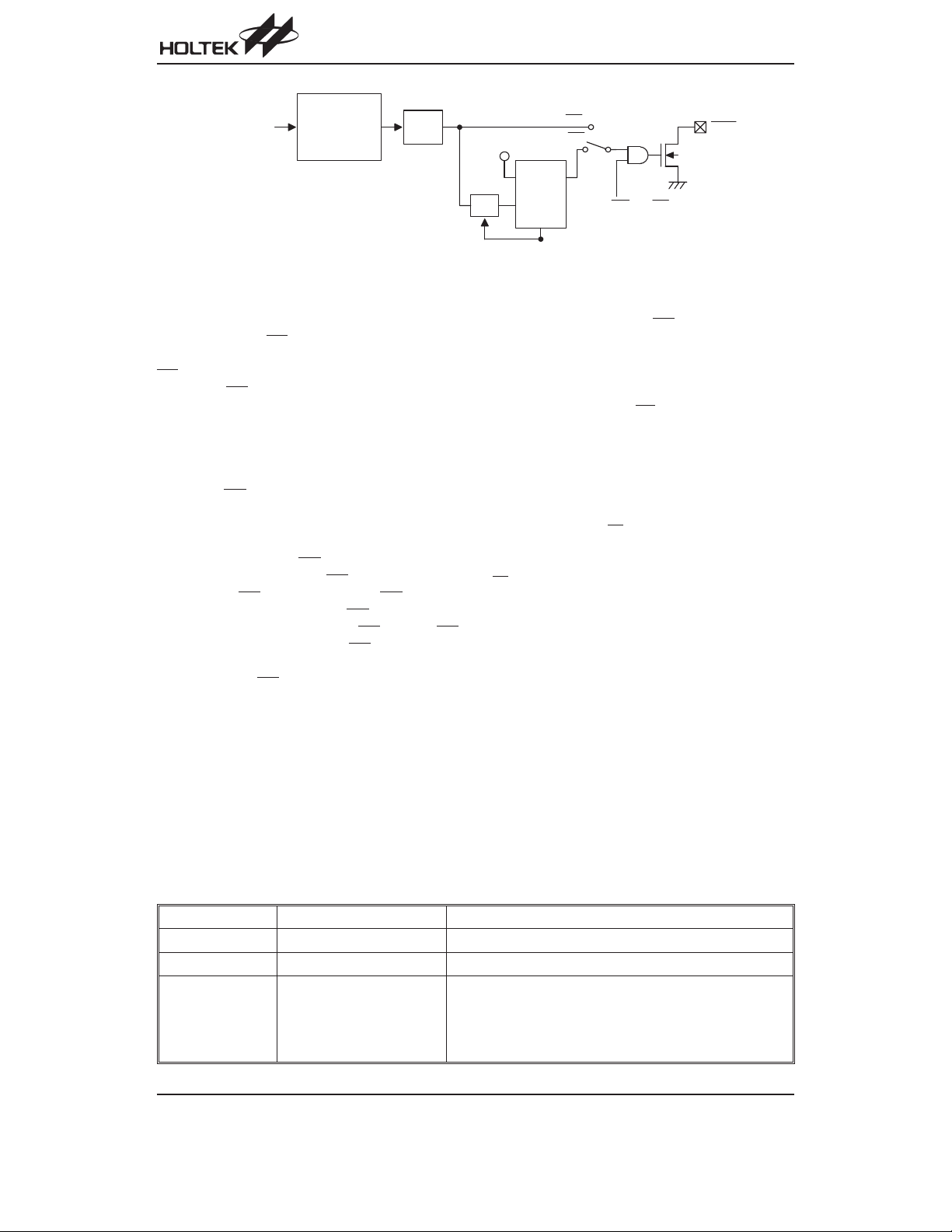
HT1621
T i m e r / W D T
S y s t e m C l o c k
f = 3 2 k H z
C l o c k S o u r c e s
n
/ 2
n = 0 ~ 7
/ 2 5 6
Timer and WDT Configurations
not only enables the time base generator but activates
the WDT time-out flag output (connect the WDT
time-out flag to the IRQ
pin). After the TIMER EN com
mand is transferred, the WDT is disconnected from the
IRQ
pin, and the output of the time base generator is con
nected to the IRQ
pin. The WDT can be cleared by execut
ing the CLR WDT command, and the contents of the time
base generator is cleared by executing the CLR WDT or
the CLR TIMER command. The CLR WDT or the CLR
TIMER command should be executed prior to the WDT
EN or the TIMER EN command respectively. Before ex
ecuting the IRQ
EN command the CLR WDT or CLR
TIMER command should be executed first. The CLR
TIMER command has to be executed before switching
from the WDT mode to the time base mode. Once the
WDT time-out occurs, the IRQ
level until the CLR WDT or the IRQ
sued. After the IRQ
output is disabled the IRQ pin will remain at the floating state. The IRQ
enabled or disabled by executing the IRQ
pin will stay at a logic low
DIS command is is-
output can be
EN or the IRQ
DIS command, respectively. The IRQ EN makes the
output ofthe time base generator or of the WDT time-out
flag appear on the IRQ
pin. The configuration of the time
base generator along with the WDT are as shown. In the
case of on-chip RC oscillator or crystal oscillator, the
power down mode can reduce power consumption
since the oscillator can be turned on or off by the corre
sponding system commands. At the power down mode
the time base/WDT loses all its functions.
On the other hand, if an external clock is selected as the
source of system frequency the SYS DIS command
turns out invalid and the power down mode fails to be
carried out. That is, after the external clock source is se
lected, the HT1621 will continue working until system
T I M E R E N / D I S
W D T E N / D I S
V
D D
Q
D
W D T
C K
/ 4
R
C L R W D T
I R Q E N / D I S
power fails or the external clock source is removed. Af
ter the system power on, the IRQ
will be disabled.
-
Tone Output
-
A simple tone generator is implemented in the HT1621.
-
The tone generator can output a pair of differential driv
ing signals on the BZ and BZ,
which are used to gener
ate a single tone. By executing the TONE4K and
TONE2K commands there are two tone frequency out
puts selectable. The TONE4K and TONE2K commands
-
set the tone frequency to 4kHz and 2kHz, respectively.
The tone output can be turned on or off by invoking the
TONE ON or the TONE OFF command. The tone out
puts, namely BZ and BZ
, are a pair of differential driving
outputs usedto drive a piezo buzzer. Once the system is
disabled or the tone output is inhibited, the BZ and the
BZ
outputs will remain at low level.
LCD Driver
The HT1621 is a 128 (32´4) pattern LCD driver. It can be
configured as 1/2 or 1/3 bias and 2 or 3 or 4 commons of
LCD driver by the S/W configuration. This feature
makes the HT1621 suitable for multiply LCD applica
tions. The LCD driving clock is derived from the system
clock. The value of the driving clock is always 256Hz even
when it is at a 32.768kHz crystal oscillator frequency, an
on-chip RC oscillator frequency, or an external fre
quency. The LCD corresponding commands are sum
marized in the table.
The bold form of100,namely 100, indicates the com
mand mode ID. If successive commands have been is
sued, the command mode ID except for the first
command, will be omitted. The LCD OFF command
turns the LCD display off by disabling the LCD bias gen
I R Q
-
-
-
-
-
-
-
-
-
-
-
Name Command Code Function
LCD OFF 10000000010X Turn off LCD outputs
LCD ON 10000000011X Turn on LCD outputs
c=0: 1/2 bias option
c=1: 1/3 bias option
BIAS & COM 1000010abXcX
ab=00: 2 commons option
ab=01: 3 commons option
ab=10: 4 commons option
Rev. 1.30 8 August 6, 2003

HT1621
erator. The LCD ON command, on the other hand, turns
the LCD display on by enabling the LCD bias generator.
The BIAS and COM are the LCD panel related com
mands. Using the LCD related commands, the HT1621
can be compatible with most types of LCD panels.
Command Format
The HT1621 can be configured by the S/W setting. There
are two mode commands to configure the HT1621 re
sources and to transfer the LCD display data. The configu
ration mode of the HT1621 is called command mode, and
its command mode ID is 100. The command mode con
sists of a system configuration command, a system
frequency selection command, a LCD configuration com
mand, a tone frequency selection command, a timer/WDT
setting command, and an operating command. The data
mode, on the other hand, includes READ, WRITE, and
READ-MODIFY-WRITE operations. The following are the
data mode IDs and the command mode ID:
Operation Mode ID
Read Data 1 1 0
Write Data 1 0 1
Read-Modify-Write Data 1 0 1
Command Command 1 0 0
The mode command should be issued before the data
or command is transferred. If successive commands
have been issued, the command mode ID, namely 100,
can be omitted. While the system is operating in the
non-successive command or the non-successive ad-
dress datamode, the CS
previous operation mode will be reset also. Once the CS
-
pin returns to ²0² a new operation mode ID should be is
sued first.
Interfacing
Only four lines are required to interface with the
HT1621. The CS
-
face circuit and to terminate the communication between
-
the host controller and the HT1621. If the CS
the data and command issued between the host controller
-
and the HT1621 are first disabled and then initialized. Be
fore issuing a mode command or mode switching, a high
-
level pulse is required to initialize the serial interface of the
HT1621. The DATA line is the serial data input/output line.
Data to be read or written or commands to be written have
to be passed through the DATA line. The RD
READ clock input. Data in the RAM are clocked out on the
falling edge of the RD
then appear on the DATA line. It is recommended that the
host controller read in correct data during the interval be
tween the rising edge and the next falling edge of the RD
signal. The WR line is the WRITE clock input. The data,
address, and command on the DATA line are all clocked
into the HT1621 on the rising edge of the WR
is an optional IRQ
the host controller and the HT1621. The IRQ
selected as a timer output or a WDT overflow flag output
by the S/W setting. The host controller can perform the
time base or the WDT function by being connected with
pin of the HT1621.
the IRQ
pin shouldbe set to ²1² and the
line is used to initialize the serial inter
signal, and the clocked out data will
line to be used as an interface between
-
-
pin is set to 1,
-
line is the
-
signal. There
pin can be
Timing Diagrams
READ Mode (Command Code:110)
C S
W R
R D
0 A 5
1
D A T A
Rev. 1.30 9 August 6, 2003
1
M e m o r y A d d r e s s 1 ( M A 1 ) D a t a ( M A 2 )
A 3 A 2
A 4
A 1
A 0
D 0 D 1
D 2
D 3
0 A 5
1
1
A 3 A 2
A 4
A 1
A 0
D 0 D 1
D 2
D 3
D a t a ( M A 1 ) M e m o r y A d d r e s s 2 ( M A 2 )
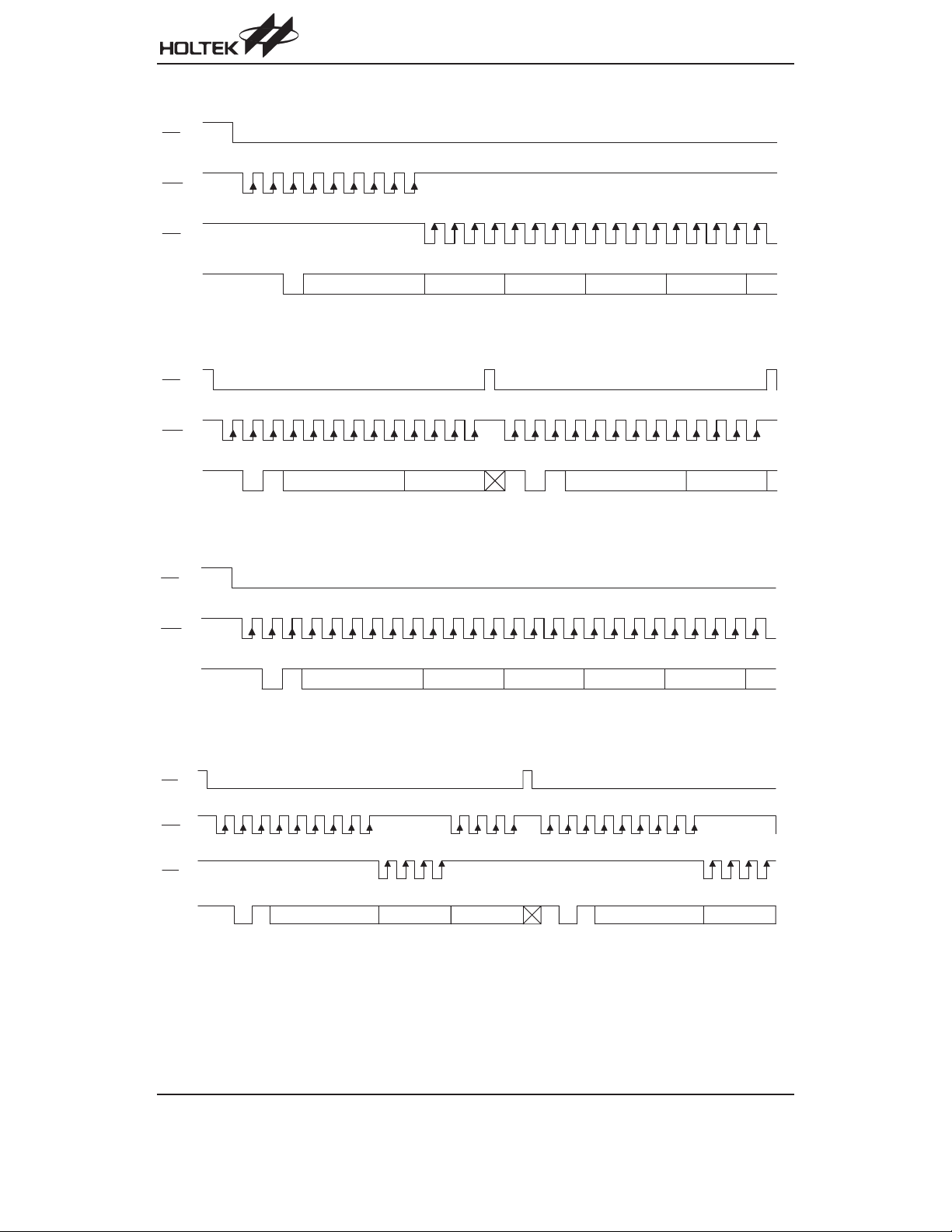
READ Mode (Successive Address Reading)
C S
W R
R D
HT1621
D A T A
0 A 5
1
1
A 3 A 2
A 4
A 1
M e m o r y A d d r e s s ( M A ) D a t a ( M A )
WRITE Mode (Command Code:101)
C S
W R
D A T A
1 A 5
1
0
M e m o r y A d d r e s s 1 ( M A 1 ) D a t a ( M A 1 )
A 3 A 2
A 4
A 1
A 0
WRITE Mode (Successive Address Writing)
C S
W R
D A T A
1 A 5
1
0
A 3 A 2
A 4
A 1
M e m o r y A d d r e s s ( M A ) D a t a ( M A )
A 0
D 0 D 1
A 0
D 0 D 1
D 0 D 1
D 0 D 1
D 2
D 3
D 2
D 3
D 0 D 1
D 2
D 3
D 0 D 1
D 2
D 3
D 0
D a t a ( M A + 1 ) D a t a ( M A + 2 ) D a t a ( M A + 3 )
D 2
D 3
1 A 5
1
0
A 3 A 2
A 4
A 1
A 0
D 0 D 1
D 2
D 3
M e m o r y A d d r e s s 2 ( M A 2 ) D a t a ( M A 2 )
D 0 D 1
D 2
D 3
D 2
D 3
D 0 D 1
D 2
D 3
D 0 D 1
D 2
D 3
D 0
D a t a ( M A + 1 ) D a t a ( M A + 2 ) D a t a ( M A + 3 )
Read-Modify-Write Mode (Command Code:101)
C S
W R
R D
A 5
D A T A
1 A 5
1
0
M e m o r y A d d r e s s 1 ( M A 1 ) D a t a ( M A 1 )
A 3 A 2
A 4
A 1
D 2
D 0 D 1
A 0
D 3
D 0 D 1
D a t a ( M A 1 )
D 2
D 3
1
1
0
A 3 A 2
A 4
M e m o r y A d d r e s s 2 ( M A 2 ) D a t a ( M A 2 )
A 1
A 0
D 0 D 1
D 2
D 3
Rev. 1.30 10 August 6, 2003
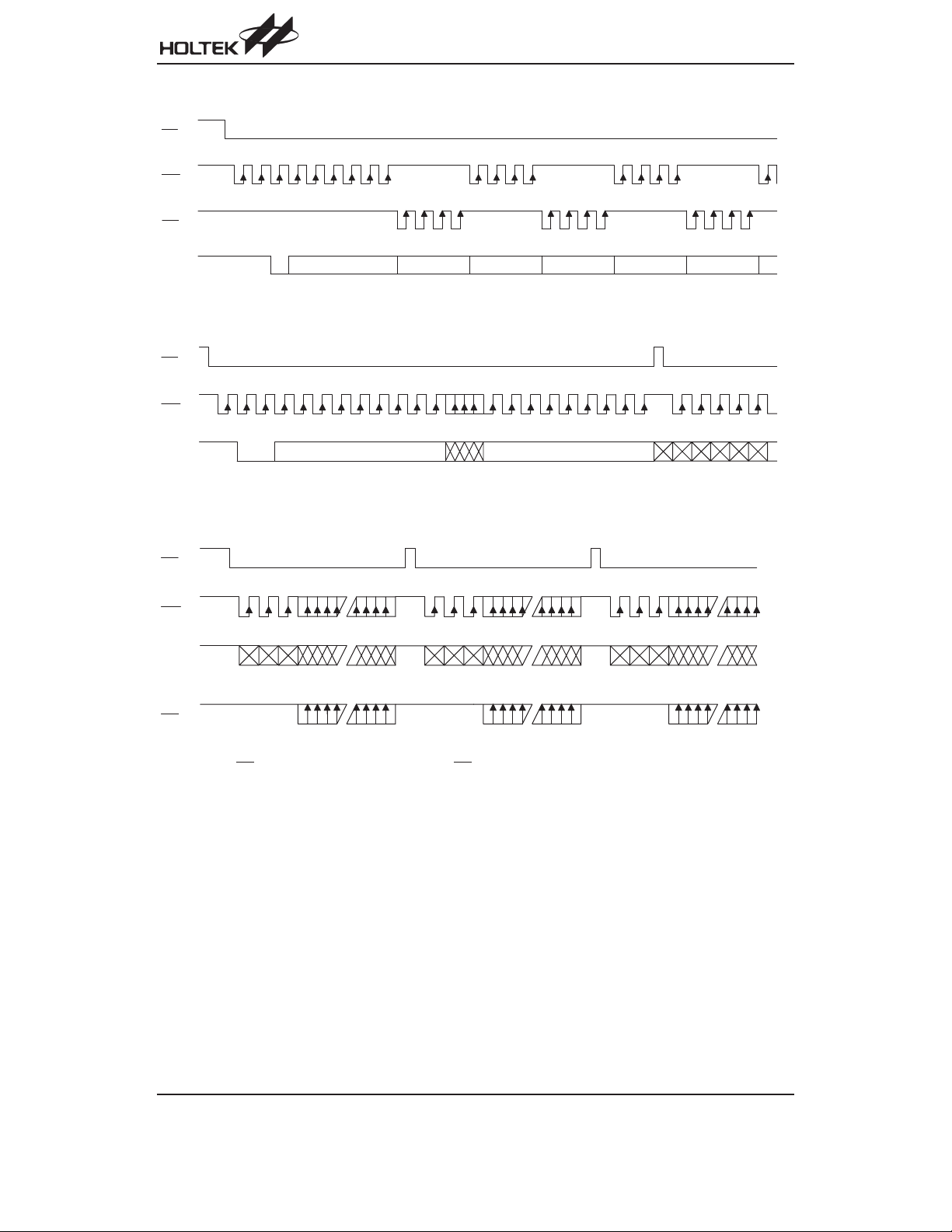
Read-Modify-Write Mode (Successive Address Accessing)
C S
W R
R D
HT1621
D A T A
1 A 5
1
0
A 3 A 2
A 4
M e m o r y A d d r e s s ( M A ) D a t a ( M A )
A 1
A 0
Command Mode (Command Code:100)
C S
W R
D A T A
0 C 8
1
0
C 7
C 6 C 5
C o m m a n d 1
C 4
C 3
Mode (Data And Command Mode)
C S
W R
D A T A
C o m m a n d
o r
D a t a M o d e
A d d r e s s & D a t a
D 0 D 1
C 2 C 1
D 2
D 3
C 0
C o m m a n d
o r
D a t a M o d e
D 2
D 0 D 1
D 3
D a t a ( M A ) D a t a ( M A + 1 ) D a t a ( M A + 1 )
C 8
C 6 C 5
C 7
A d d r e s s a n d D a t a
D 2
D 0 D 1
C o m m a n d iC o m m a n d . . . C o m m a n d
D 3
C 4
C 2 C 1
C 3
D 2
D 0 D 1
C 0
C o m m a n d
o r
D a t a M o d e
D 3
D a t a M o d e
D 2
D 0
D 1
D a t a ( M A + 2 )
o r
A d d r e s s a n d D a t a
D 3
D 0
R D
Note: It is recommended that the host controller should read in the data from the DATA line between the rising edge
of the RD
line and the falling edge of the next RD line.
Rev. 1.30 11 August 6, 2003
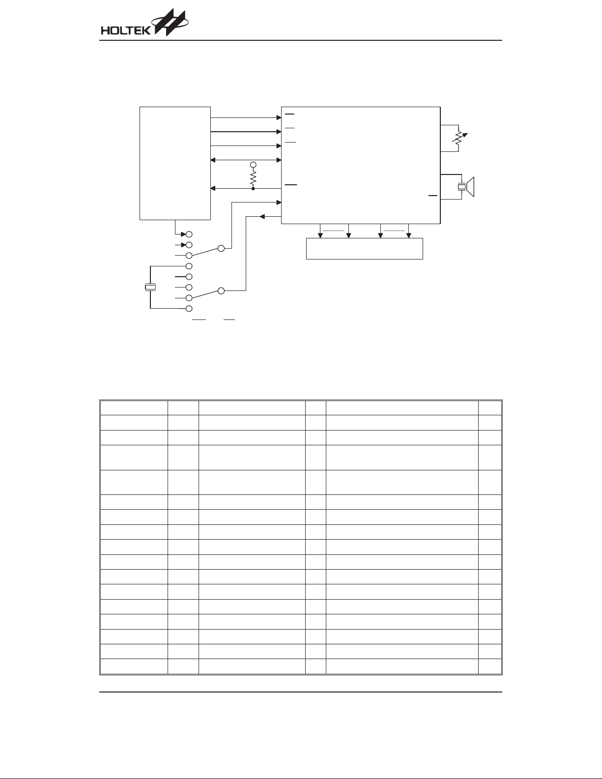
Application Circuits
Host Controller with an HT1621 Display System
HT1621
C S
*
R D
W R
M C U
C l o c k O u t
E x t e r n a l C o l c k 1
E x t e r n a l C o l c k 2
O n - c h i p O S C
C r y s t a l
3 2 7 6 8 H z
Note: The connection of IRQ
The voltage applied to V
Adjust VR to fit LCD display, at V
and RD pin can be selected depending on the requirement of the MCU.
pin must be lower than VDD.
LCD
=5V, V
DD
D A T A
*
R
I R Q
O S C I
O S C O
=4V, VR=15kW±20%.
LCD
Adjust R (external pull-high resistance) to fit user’s time base clock.
Command Summary
H T 1 6 2 1 B
C O M 0 ~ C O M 3 S E G 0 ~ S E G 3 1
1 / 2 o r 1 / 3 B i a s ; 1 / 2 , 1 / 3 o r 1 / 4 D u t y
L C D P a n e l
V D D
V L C D
*
V R
B Z
P i e z o
B Z
Name ID Command Code D/C Function Def.
READ 110 A5A4A3A2A1A0D0D1D2D3 D Read data from the RAM
WRITE 101 A5A4A3A2A1A0D0D1D2D3 D Write data to the RAM
READ-MODIFYWRITE
SYS DIS 100 0000-0000-X C
101 A5A4A3A2A1A0D0D1D2D3 D READ and WRITE to the RAM
Turn off both system oscillator and LCD
bias generator
Yes
SYS EN 100 0000-0001-X C Turn on system oscillator
LCD OFF 100 0000-0010-X C Turn off LCD bias generator Yes
LCD ON 100 0000-0011-X C Turn on LCD bias generator
TIMER DIS 100 0000-0100-X C Disable time base output
WDT DIS 100 0000-0101-X C Disable WDT time-out flag output
TIMER EN 100 0000-0110-X C Enable time base output
WDT EN 100 0000-0111-X C Enable WDT time-out flag output
TONE OFF 100 0000-1000-X C Turn off tone outputs Yes
TONE ON 100 0000-1001-X C Turn on tone outputs
CLR TIMER 100 0000-11XX-X C Clear the contents of time base generator
CLR WDT 100 0000-111X-X C Clear the contents of WDT stage
XTAL 32K 100 0001-01XX-X C System clock source, crystal oscillator
Rev. 1.30 12 August 6, 2003
HT1621
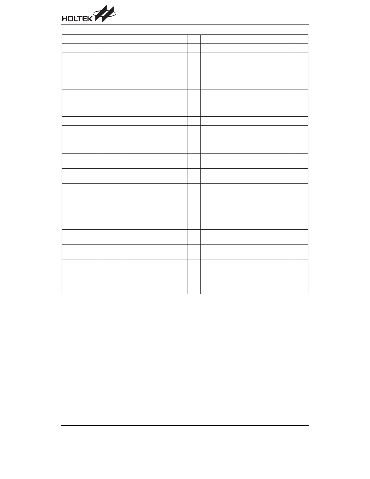
Name ID Command Code D/C Function Def.
RC 256K 100 0001-10XX-X C System clock source, on-chip RC oscillator Yes
EXT 256K 100 0001-11XX-X C System clock source, externalclock source
LCD 1/2 bias option
BIAS 1/2 100 0010-abX0-X C
BIAS 1/3 100 0010-abX1-X C
TONE 4K 100 010X-XXXX-X C Tone frequency, 4kHz
TONE 2K 100 011X-XXXX-X C Tone frequency, 2kHz
IRQ
DIS 100 100X-0XXX-X C Disable IRQ output Yes
IRQ
EN 100 100X-1XXX-X C Enable IRQ output
F1 100 101X-X000-X C
F2 100 101X-X001-X C
F4 100 101X-X010-X C
F8 100 101X-X011-X C
F16 100 101X-X100-X C
F32 100 101X-X101-X C
F64 100 101X-X110-X C
F128 100 101X-X111-X C
TEST 100 1110-0000-X C
NORMAL 100 1110-0011-X C Normal mode Yes
ab=00: 2 commons option
ab=01: 3 commons option
ab=10: 4 commons option
LCD 1/3 bias option
ab=00: 2 commons option
ab=01: 3 commons option
ab=10: 4 commons option
Time base/WDT clock output:1Hz
The WDT time-out flag after: 4s
Time base/WDT clock output:2Hz
The WDT time-out flag after: 2s
Time base/WDT clock output:4Hz
The WDT time-out flag after: 1s
Time base/WDT clock output:8Hz
The WDT time-out flag after: 1/2s
Time base/WDT clock output:16Hz
The WDT time-out flag after: 1/4s
Time base/WDT clock output:32Hz
The WDT time-out flag after: 1/8s
Time base/WDT clock output:64Hz
The WDT time-out flag after: 1/16s
Time base/WDT clock output:128Hz
The WDT time-out flag after: 1/32s
Test mode, user don¢t use.
Yes
Note: X : Don,t care
A5~A0 : RAM addresses
D3~D0 : RAM data
D/C : Data/command mode
Def. : Power on reset default
All the bold forms, namely 110, 101, and 100, are mode commands. Of these, 100indicates the command
mode ID. If successive commands have been issued, the command mode ID except for the first command will
be omitted. The source of the tone frequency and of the time base/WDT clock frequency can be derived from
an on-chip 256kHz RC oscillator, a 32.768kHz crystal oscillator, or an external 256kHz clock. Calculation of the
frequency is based on the system frequency sources as stated above. It is recommended that the host control
ler should initialize the HT1621 after power on reset, for power on reset may fail, which in turn leads to the mal
functioning of the HT1621.
Rev. 1.30 13 August 6, 2003
-
-

Package Information
48-pin SSOP (300mil) Outline Dimensions
HT1621
4 8
A
1
C
C '
D
E
Symbol
Min. Nom. Max.
A 395
B 291
C8
C¢
613
D85
E
¾
F4
G25
H4
2 5
B
2 4
F
Dimensions in mil
¾
¾
¾
¾
¾
25
¾
¾
¾
G
a
a 0°¾8°
H
420
299
12
637
99
¾
10
35
12
Rev. 1.30 14 August 6, 2003
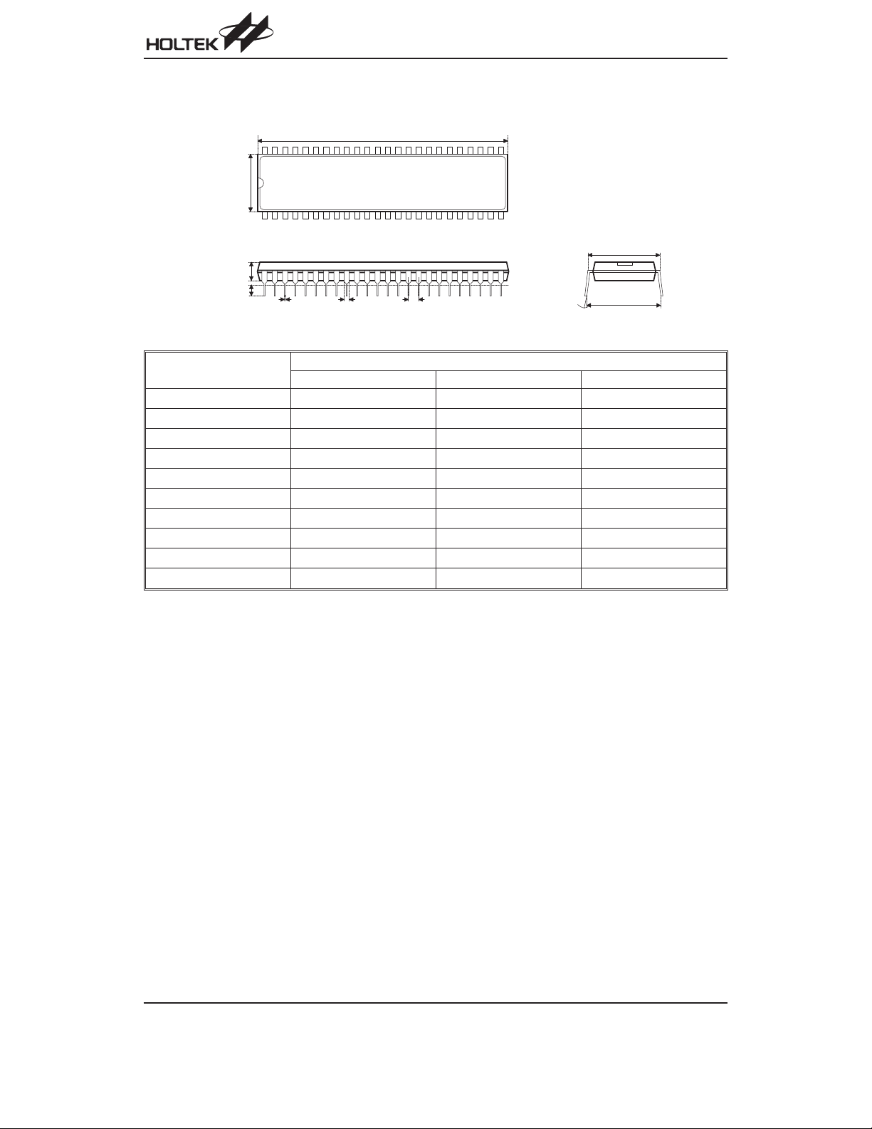
48-pin DIP (600mil) Outline Dimensions
HT1621
A
4 8
B
1
C
D
Symbol
E
F
Min. Nom. Max.
G
A 2435
B 535
C 145
D 125
E16
F50
G
¾
H 595
I 635
2 5
2 4
a
Dimensions in mil
¾
¾
¾
¾
¾
¾
100
¾
¾
a 0°¾15°
H
I
2445
555
155
145
20
70
¾
615
670
Rev. 1.30 15 August 6, 2003

48-pin LQFP (7´7) Outline Dimensions
J
HT1621
C
H
G
K
3 6 2 5
3 7
A
B
4 8
Symbol
A 8.90
B 6.90
C 8.90
D 6.90
E
F
G 1.35
H
I
J 0.45
K 0.10
D
2 4
F
E
1 3
1 21
Dimensions in mm
Min. Nom. Max.
¾
¾
¾
¾
¾
¾
0.50
0.20
¾
¾¾
¾
0.10
¾
¾
a 0°¾7°
I
a
9.10
7.10
9.10
7.10
¾
¾
1.45
1.60
¾
0.75
0.20
Rev. 1.30 16 August 6, 2003

28-pin SKDIP (300mil) Outline Dimensions
A
HT1621
Symbol
1
C
D
E
F
Min. Nom. Max.
2 8
B
A 1375
B 278
C 125
D 125
E16
F50
G
¾
H 295
I 330
1 5
1 4
H
G
a
I
Dimensions in mil
¾
¾
¾
¾
¾
¾
100
¾
¾
a 0°¾15°
1395
298
135
145
20
70
¾
315
375
Rev. 1.30 17 August 6, 2003
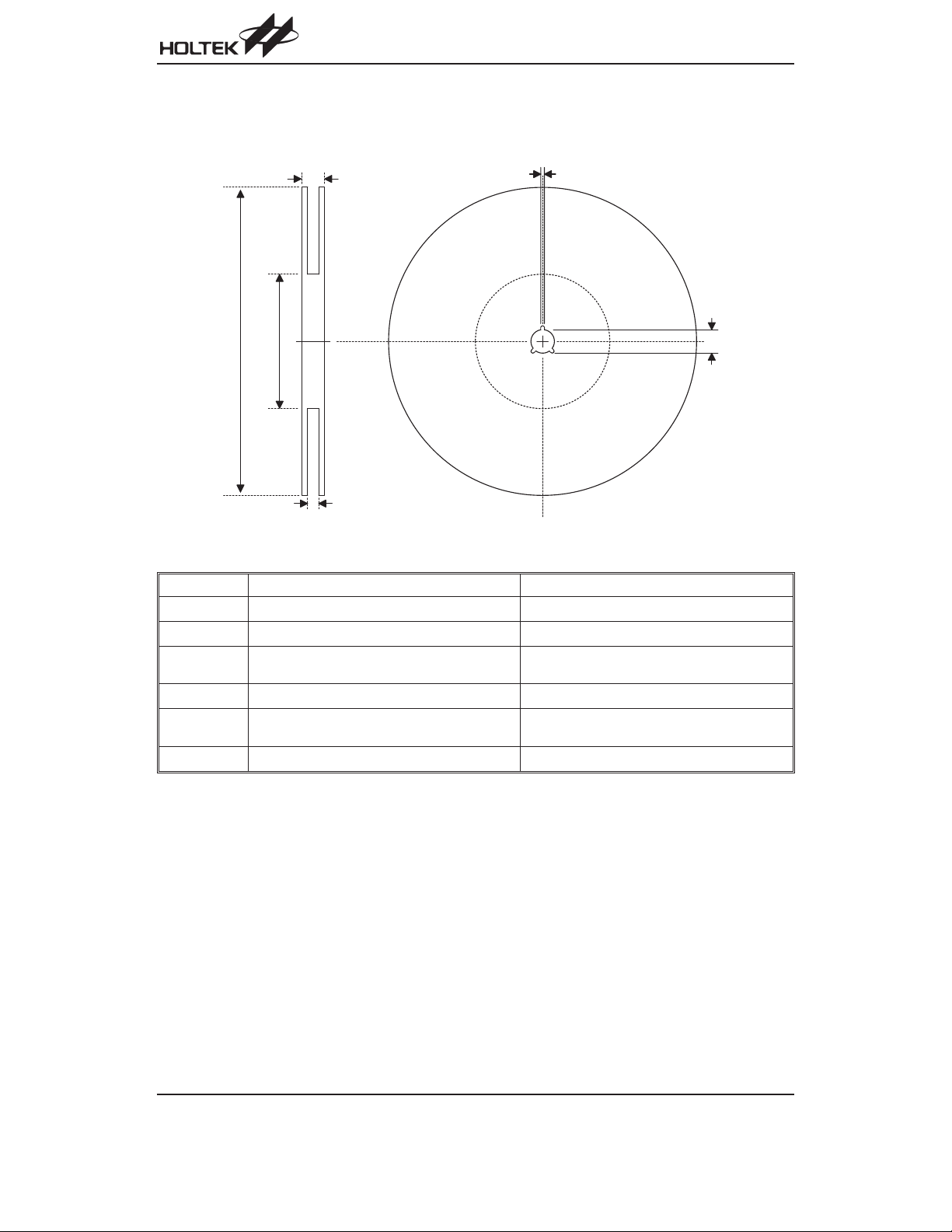
Product Tape and Reel Specifications
Reel Dimensions
HT1621
T 2
A
B
T 1
D
SSOP 48W
Symbol Description Dimensions in mm
A Reel Outer Diameter
B Reel Inner Diameter
C Spindle Hole Diameter
D Key Slit Width
T1 Space Between Flange
T2 Reel Thickness
330±1.0
100±0.1
13.0+0.5
2.0±0.5
32.2+0.3
38.2±0.2
C
-0.2
-0.2
Rev. 1.30 18 August 6, 2003

Carrier Tape Dimensions
HT1621
D
E
F
PD 1
P 1P 0
W
A 0
B 0
C
SSOP 48W
Symbol Description Dimensions in mm
W Carrier Tape Width
P Cavity Pitch
E Perforation Position
F Cavity to Perforation (Width Direction)
32.0±0.3
16.0±0.1
1.75±0.1
14.2±0.1
D Perforation Diameter 2.0 Min.
D1 Cavity Hole Diameter 1.5+0.25
P0 Perforation Pitch
P1 Cavity to Perforation (Length Direction)
A0 Cavity Length
B0 Cavity Width
K1 Cavity Depth
K2 Cavity Depth
t Carrier Tape Thickness
4.0±0.1
2.0±0.1
12.0±0.1
16.20±0.1
2.4±0.1
3.2±0.1
0.35±0.05
C Cover Tape Width 25.5
t
K 1
K 2
Rev. 1.30 19 August 6, 2003

HT1621
Holtek Semiconductor Inc. (Headquarters)
No.3, Creation Rd. II, Science-based Industrial Park, Hsinchu, Taiwan
Tel: 886-3-563-1999
Fax: 886-3-563-1189
http://www.holtek.com.tw
Holtek Semiconductor Inc. (Sales Office)
11F, No.576, Sec.7 Chung Hsiao E. Rd., Taipei, Taiwan
Tel: 886-2-2782-9635
Fax: 886-2-2782-9636
Fax: 886-2-2782-7128 (International sales hotline)
Holtek Semiconductor (Shanghai) Inc.
7th Floor, Building 2, No.889, Yi Shan Rd., Shanghai, China
Tel: 021-6485-5560
Fax: 021-6485-0313
http://www.holtek.com.cn
Holtek Semiconductor (Hong Kong) Ltd.
Block A, 3/F, Tin On Industrial Building, 777-779 Cheung Sha Wan Rd., Kowloon, Hong Kong
Tel: 852-2-745-8288
Fax: 852-2-742-8657
Holmate Semiconductor, Inc.
46712 Fremont Blvd., Fremont, CA 94538
Tel: 510-252-9880
Fax: 510-252-9885
http://www.holmate.com
Copyright Ó 2003 by HOLTEK SEMICONDUCTOR INC.
The information appearing in this Data Sheet is believed to be accurate at the time of publication. However, Holtek as
sumes no responsibility arising from the use of the specifications described. The applications mentioned herein are used
solely for the purpose of illustration and Holtek makes no warranty or representation that such applications will be suitable
without further modification, nor recommends the use of its products for application that may present a risk to human life
due to malfunction or otherwise. Holtek¢s products are not authorized for use as critical components in life support devices
or systems. Holtek reserves the right to alter its products without prior notification. For the most up-to-date information,
please visit our web site at http://www.holtek.com.tw.
-
Rev. 1.30 20 August 6, 2003
 Loading...