

Features
Operating voltage: 2.0V~5.5V
·
Maximum input serial clock: 500kHz at
·
V
=2V, 2MHz at VDD=5V
DD
Operating current: less than 400nA at 2V,
·
less than 1.2mAat5V
TTL compatible
·
-
VIH: 2.0V~VDD+0.3V at VDD=5V
-
VIL: -0.3V~+0.8V at VDD=5V
Applications
Microcomputer serial clock
·
General Description
The HT1380/HT1381 is a serial timekeeper IC
which provides seconds, minutes, hours, day,
date, month and year information. The number
of days in each month and leap years are auto
matically adjusted. The HT1380/HT1381 is de
signed for low power consumption and can
operate in two modes: one is the 12-hour mode
with an AM/PM indicator, the other is the
24-hour mode.
HT1380/HT1381
Serial Timekeeper Chip
Two data transmission modes: single-byte,
·
or burst mode
Serial I/O transmission
·
All registers store BCD format
·
HT1380: 8-pin DIP package
·
HT1381: 8-pin SOP package
Clock and Calendar
·
The HT1380/HT1381 has several registers to
store the corresponding information with 8-bit
data format. A 32768Hz crystal is required to
provide the correct timing. In order to minimize
the pin number, the HT1380/HT1381 use a se
rial I/O transmission method to interface with a
microprocessor. Only three wires are required:
(1) REST
livered 1 byte at a time or in a burst of up to 8
bytes.
, (2) SCLK and (3) I/O. Data can be de-
-
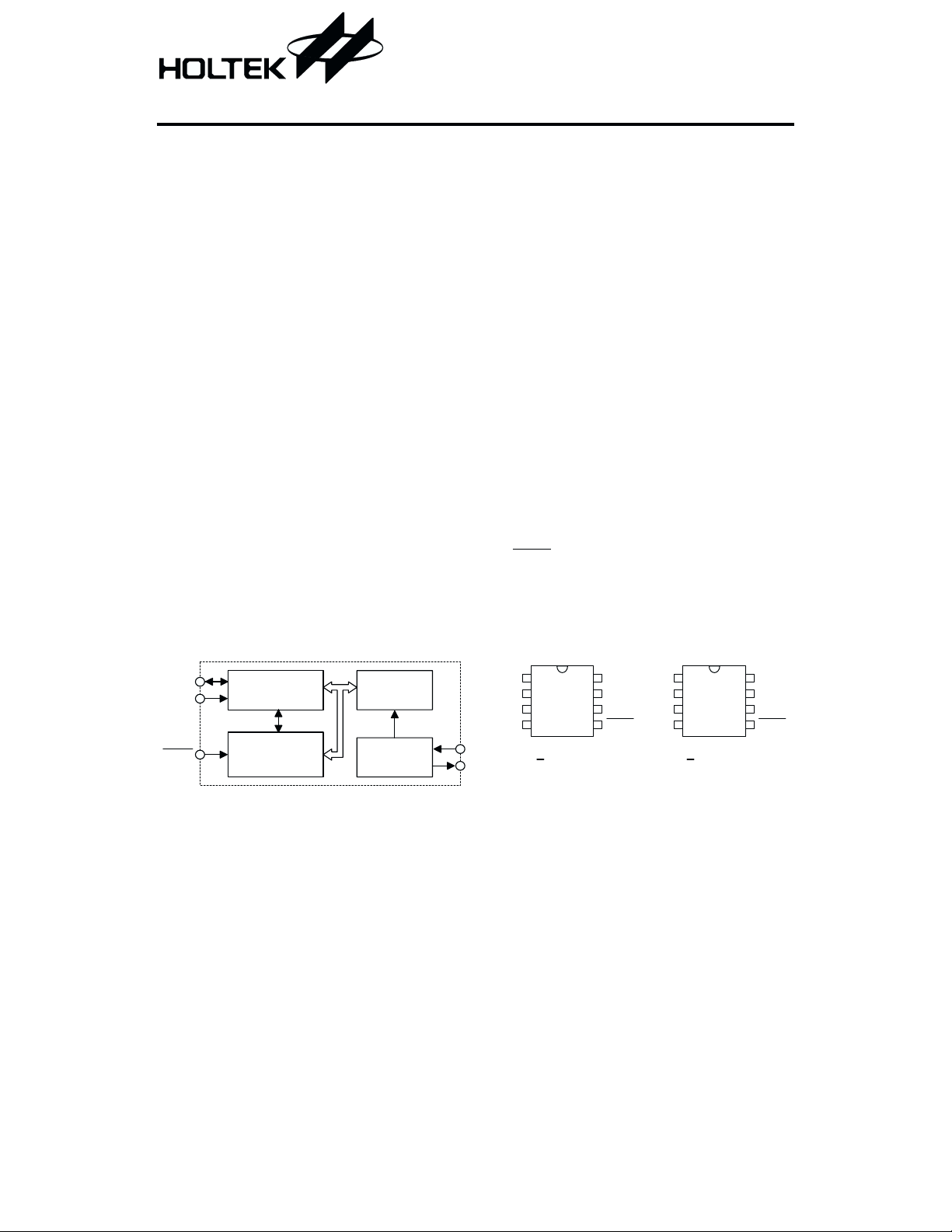
Block Diagram Pin Assignment
I/O
SCLK
REST
Data Shift
R egister
Command
C ontrol Logic
R eal Tim e
Clock
O s c illa to r a n d
Divider
Circuit
1
NC
2
X1
3
X2
4
VSS
X1
X2
1 September 18, 2000
H T1380
8 D IP
VDD
8
7
SCLK
I/O
6
REST
5
NC
VSS
X1
X2
1
2
3
4
H T1381
8 S O P
VDD
8
7
SCLK
I/O
6
REST
5
HT1380/HT1381
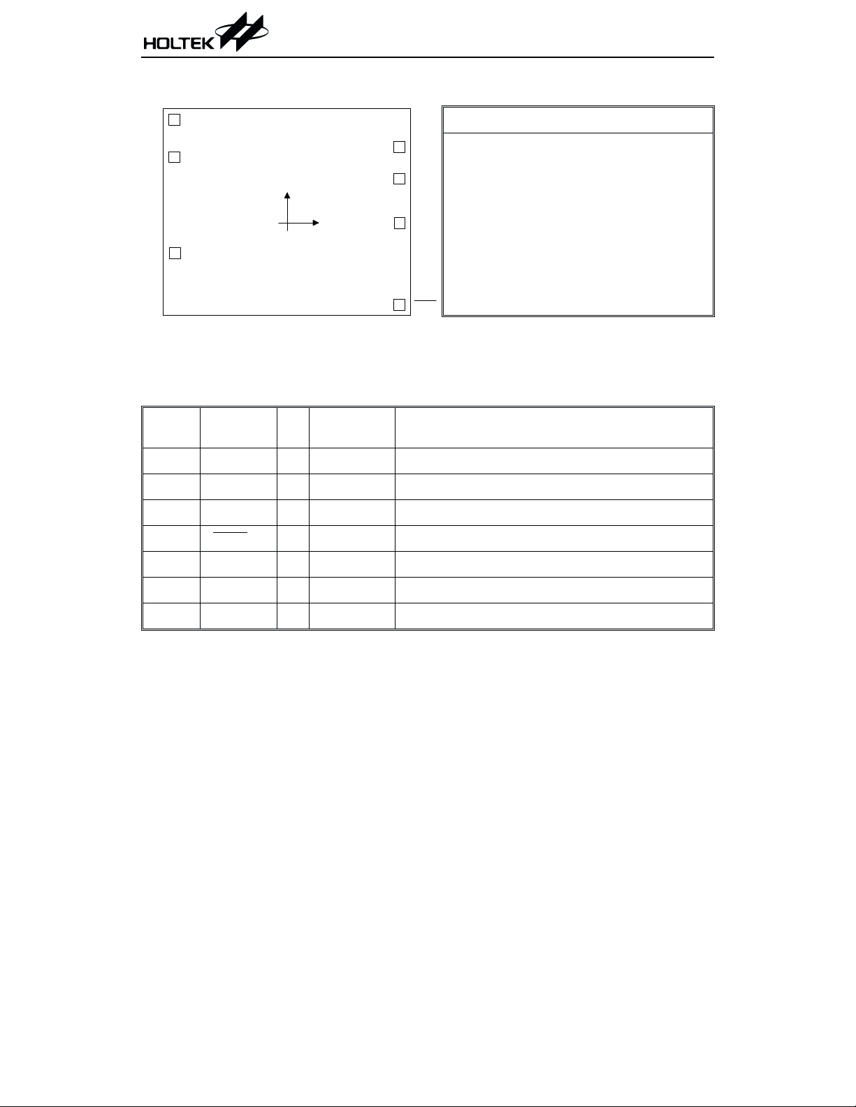
Pad Assignment Pad Coordinates
1
VSS
X1
7
X2
2
(0 ,0 )
3
VDD
6
SCLK
5
I/O
Pad No. X Y
1
2
3
-851.40
-851.40
-844.40 -203.90
4 845.90
5 848.40
6 845.90 332.60
7 844.40 572.60
Chip size: 2010 ´ 1920 (mm)
4
REST
2
* The IC substrate should be connected to VSS in the PCB layout artwork.
Pad Description
Pad No. Pad Name I/O
1 X1 I CMOS 32768Hz crystal input pad
2 X2 O CMOS Oscillator output pad
Internal
Connection
Description
Unit: mm
775.00
494.60
-618.30
-4.30
3 VSS
4 REST
¾
I CMOS Reset pin with serial transmission
CMOS Negative power supply, ground
5 I/O I/O CMOS Data input/output pin with serial transmission
6 SCLK I CMOS Serial clock pulse pin with serial transmission
7 VDD
¾
CMOS Positive power supply
Absolute Maximum Ratings
Supply Voltage..............................-0.3V to 5.5V
Input Voltage .................V
-0.3V to VDD+0.3V
SS
Note: These are stress ratings only. Stresses exceeding the range specified under ²Absolute Maxi
mum Ratings² may cause substantial damage to the device. Functional operation of this de
vice at other conditions beyond those listed in the specification is not implied and prolonged
exposure to extreme conditions may affect device reliability.
Storage Temperature.................-50°Cto125°C
Operating Temperature ..................0°Cto70°C
2 September 18, 2000
-
-
HT1380/HT1381
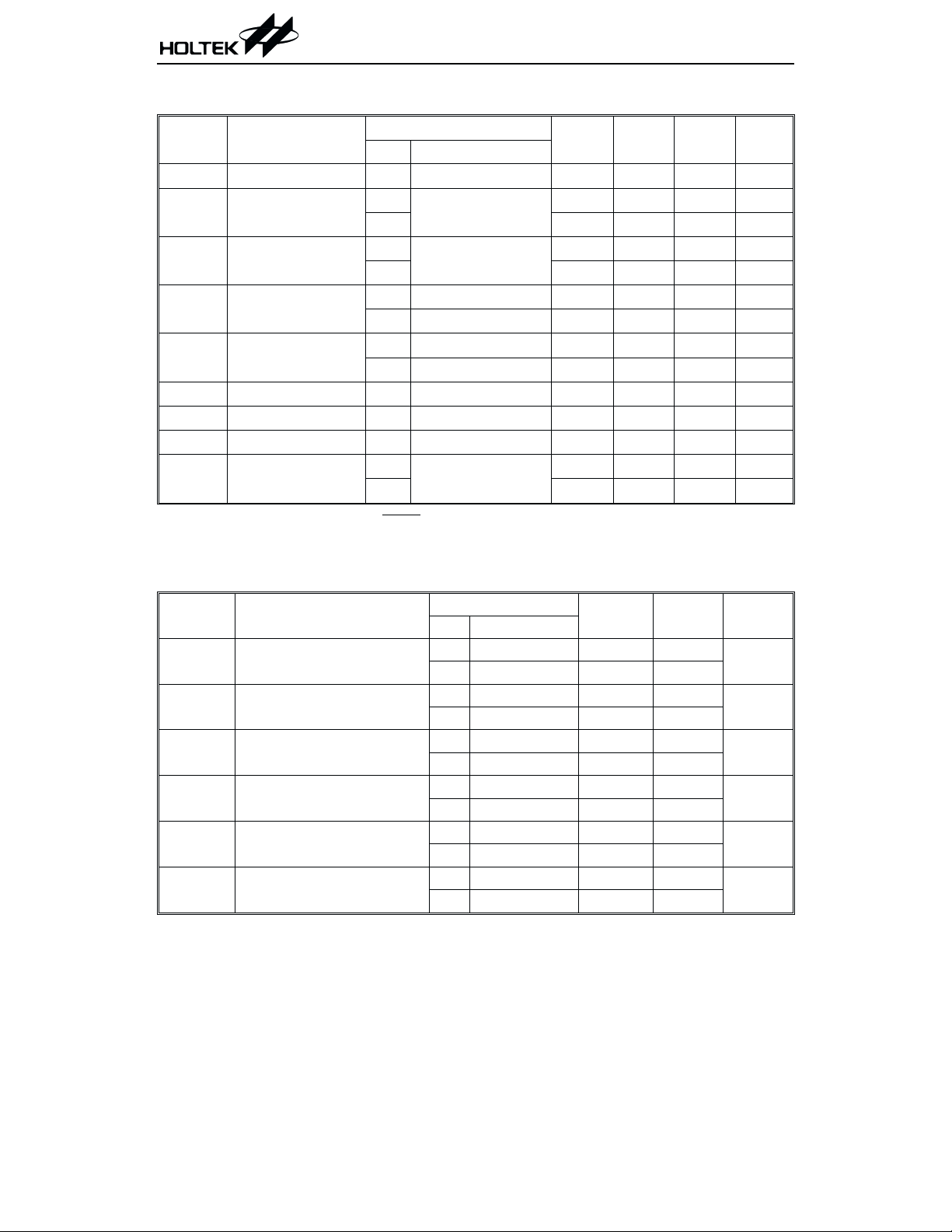
D.C. Characteristics
Symbol Parameter
* I
V
DD
I
STB
I
DD
I
OH
I
OL
V
IH
V
IL
f
OSC
f
SCLK
STB
Operating Voltage
Standby Current
Operating Current
Source Current
Sink Current
²H² Input Voltage
²L² Input Voltage
System Frequency 5V
Serial Clock
is specified with SCLK, I/O, REST open. The clock halt bit must be set to logic 1 (oscillator
disabled).
Test Conditions
V
DD
Conditions
¾¾
2V
5V
2V
5V
2V
5V
2V
5V
5V
5V
No load
V
V
V
V
¾
=1.8V
OH
=4.5V
OH
=0.2V
OL
=0.5V
OL
¾
¾¾¾
32768Hz X¢TAL ¾
2V
5V
¾
Min. Typ. Max. Unit
2
¾
¾¾
¾¾
¾
¾
0.7 1.0
0.7 1.2
-0.2 -0.4 ¾
-0.5 -1.0 ¾
0.7 1.5
2.0 4.0
2
¾¾
32768
¾¾
¾¾
Ta=25°C
5.5 V
100 nA
100 nA
mA
mA
mA
mA
¾
¾
mA
mA
V
0.8 V
¾
Hz
0.5 MHz
2 MHz
A.C. Characteristics
Symbol Parameter
t
DC
t
CDH
t
CDD
t
CL
t
CH
f
CLK
Data to Clock Setup
Clock to Data Hold
Clock to Data Delay
Clock Low Time
Clock High Time
Clock Frequency
Test Conditions
V
Conditions
DD
2V
5V
2V
5V
2V
5V
2V
5V
2V
5V
2V
5V
¾
¾
¾
¾
¾¾
¾¾
¾
¾
¾
¾
¾¾
¾
3 September 18, 2000
Min. Max. Unit
200
50
280
70
¾
¾
¾
¾
800
200
1000
250
1000
250
¾
¾
¾
¾
0.5
D.C. 2.0
Ta=25°C
ns
ns
ns
ns
ns
MHz

HT1380/HT1381
Symbol Parameter
t
r
t
f
t
CC
t
CCH
t
CWH
t
CDZ
Clock Rise and Fall Time
Reset to Clock Setup
Clock to Reset Hold
Reset Inactive Time
Reset to I/O High Impedance
Test Conditions
V
DD
2V
5V
2V
5V
2V
5V
2V
5V
2V
5V
Functional Description
The HT1380/HT1381 mainly contains the fol
lowing internal elements: a data shift register
array to store the clock/calendar data, com
mand control logic, oscillator circuit and read
timer clock. The clock is contained in eight
read/write registers as shown below. Data con
tained in the clock register is in binary coded
decimal format.
Two modes are available for transferring the
data between the microprocessor and the
Conditions
¾¾
¾¾
¾
¾
¾
¾
¾
¾
¾¾
¾¾
HT1380/HT1381. One is in single-byte mode
-
Min. Max. Unit
2000
500
4
1
240
60
4
1
¾
¾
¾
¾
¾
¾
280
70
and the other is in multiple-byte mode.
The HT1380/HT1381 also contains two addi
tional bits, the clock halt bit (CH) and the write
protect bit (WP). These bits control the opera
tion of the oscillator and so data can be written
to the register array. These two bits should first
be specified in order to read from and write to
the register array properly.
ns
us
ns
us
ns
-
-
Command byte
For each data transfer, a Command Byte is initiated to specify which register is accessed. This is to
determine whether a read, write, or test cycle is operated and whether a single byte or burst mode
transfer is to occur. Refer to the table shown below and follow the steps to write the data to the chip.
First give a Command Byte of HT1380/HT1381, and then write a data in the register.
This table illustrates the correlation between Command Byte and their bits:
Command Byte
Function Description C7 C6 C5 C4 C3 C2 C1 C0
Select Read or Write Cycle R/W
Specify the Register to be Accessed A2 A1 A0
Clock Halt Flag C
For IC Test Only 1001xxx1
Select Single Byte or Burst Mode 1011111x
Note: ²x² stands for don¢t care
4 September 18, 2000

The following table shows the register address and its data format:
Register
Name
Seconds 00~59 CH 10 SEC SEC 000
Minutes 00~59 0 10 MIN MIN 001
Hours
Date 01~31 0 0 10 DATE DATE 011
Month 01~12 0 0 0 10M MONTH 100
Day 01~07 0 0 0 0 DAY 101
Year 00~99 10 YEAR YEAR 110
Write
Protect
Range
Data
01~12
00~23
00~80 WP ALWAYS ZERO 111
D7 D6 D5 D4 D3 D2 D1 D0
12\2400AP10HR
Register Definition
HR
HOUR 010
Address
A2~A0
HT1380/HT1381
Bit
Command
R/W
W
R
W
R
W
R
W
R
W
R
W
R
W
R
W
R
Byte
10000000
10000001
10000010
10000011
10000100
10000101
10000110
10000111
10001000
10001001
10001010
10001011
10001100
10001101
10001110
10001111
CH:
Clock Halt bit
CH=0 oscillator enabled
CH=1 oscillator disabled
Write protect bit
WP:
WP=0 register data can be written in
WP=1 register data can not be written in
Bit 7 of Reg2:
Bit 5 of Reg2:
R/W signal
The LSB of the Command Byte determines
whether the data in the register be read or be
written to.
When it is set as ²0² means that a write cycle is
to take place otherwise this chip will be set into
the read mode.
12/24 mode flag
bit 7=1, 12-hour mode
bit 7=0, 24-hour mode
AM/PM mode defined
AP=1 PM mode
AP=0 AM mode
A0~A2
A0 to A2 of the Command Byte is used to specify
which registers are to be accessed. There are
eight registers used to control the month data,
etc., and each of these registers have to be set as
a write cycle in the initial time.
Burst mode
When the Command Byte is 10111110 (or
10111111) , the HT1380/HT1381 is configured in
burst mode. In this mode the eight clock/calen
dar registers can be written (or read) in series,
starting with bit 0 of register address 0 (see the
timing on the next page).
Test mode
When the Command Byte is set as 1001xxx1,
HT1380/HT1381 is configured in test mode.
The test mode is used by Holtek only for testing
purposes. If used generally, unpredictable con
ditions may occur.
5 September 18, 2000
-
-

HT1380/HT1381
Write protect register
This register is used to prevent a write opera
tion to any other register. Data can be written
into the designated register only if the Write
Protect signal (WP) is set to logic 0. The Write
Protect Register should be set first before re
starting the system or before writing the new
data to the system, and it should set as logic 1 in
the read cycle. The Write Protect bit cannot be
written to in the burst mode.
Clock Halt bit
D7 of the Seconds Register is defined as the
Clock Halt Flag (CH).
When this bit is set to logic 1, the clock oscilla
tor is stopped and the chip goes into a
low-power standby mode. When this bit is writ
ten to logic 0, the clock will start.
12-hour/24-hour mode
The D7 of the hour register is defined as the
12-hour or 24-hour mode select bit.
When this bit is in high level, the 12-hour mode
is selected otherwise it¢s the 24-hour mode.
AM-PM mode
These are two functions for the D5 of the hour
register determined by the value D7 of the same
register.
One is used in AM/PM selection on the 12-hour
mode. When D5 is logic 1, it is PM, otherwise
it¢s AM. The other is used to set the second
10-hour bit (20~23 hours) on the 24-hour mode.
Reset and Serial Clock control
The REST
pin is used to allow access data to the
shift register like a toggle switch. When the
REST
pin is taken high, the built-in control
logic is turned on and the address/command se
quence can access the corresponding shift regis
ter. The REST pin is also used to terminate
either single-byte or burst mode data format.
The input signal of SCLK is a sequence of a fall
ing edge followed by a rising edge and it is used
to synchronize the register data whether read
or write. For data input, the data must be read
after the rising edge of SCLK. The data on the
I/O pin becomes output mode after the falling
edge of the SCLK. All data transfer terminates
if the REST
pin is low and the I/O pin goes to a
high impedance state. The data transfer is il
lustrated on the next page.
Data in and Data out
In writing a data byte with HT1380/HT1381,
the read/write should first set as R/W=0 in the
Command Byte and follow with the correspond
ing data register on the rising edge of the next
eight SCLK cycles. Additional SCLK cycles are
ignored. Data inputs are entered starting with
bit 0.
In reading a data on the register of
HT1380/HT1381, R/W=1 should first be en
tered as input. The data bit outputs on the fall
ing edge of the next eight SCLK cycles. Note
that the first data bit to be transmitted on the
first falling edge after the last bit of the read
command byte is written. Additional SCLK cycles re-transmits the data bytes as long as
REST
remains at high level. Data outputs are
read starting with bit 0.
Crystal selection
A 32768Hz crystal can be directly connected to
the HT1380/HT1381 via pin 2 and pin 3 (X1,
X2). In order to obtain the correct frequency,
two additional load capacities (C1, C2) are
needed. The value of the capacity depends on
how accurate the crystal is. We suggest that
you can follow the table on the next page.
32768H z
-
X1
-
C1 C2
-
-
-
-
-
X2
6 September 18, 2000

The following diagram shows the single and burst mode transfer:
Single byte transfer
SCLK
REST
0 1 2 3 4 5 6 7 0 1 2 3 4 5 6 7
HT1380/HT1381
I/O
R/W A0 A1 A2 0 0 1
0
COM M AND BYTE
D A T A I/O
B u rs t m o d e tra n s fe r
SCLK
REST
0 1 2 3 4 5 6 7
I/O
R/W
11111
COM M AND BYTE DATA BYTE7DATA BYTE0
07 07
01
The table illustrates the values suggested for capacities C1, C2
Part No. Crystal Error Capacity Value
±10ppm
5pF
HT1380/HT1381
10~20ppm 8pF
Operating flowchart
To initiate any transfer of data, REST
is taken high and an 8-bit command byte is first loaded into the
control logic to provide the register address and command information. Following the command
word, the clock/calendar data is serially transferred to or from the corresponding register. The REST
pin must be taken low again after the transfer operation is completed. All data enter on the rising
edge of SCLK and outputs on the falling edge of SCLK. In total, 16 clock pulses are needed for a sin
gle byte mode and 72 for burst mode. Both input and output data starts with bit 0.
In using the HT1380/HT1381, set first the WP and CH to 0 and wait for about 3 seconds, the oscilla
tor will generate the clocks for internal use. Then, choose either single mode or burst mode to input
the data. The read or write operating flowcharts are shown on the next page.
-
-
7 September 18, 2000

To disable the write
·
protect (WP=0) bit and
enable the oscillator
(CH=0)
Single byte data
·
transfer
Burst mode data
·
transfer
HT1380/HT1381
START
Set R EST pin
from low to high
In p u t th e w rite
protect com m and
byte 8EH
D isable the w rite
protect bit (W P)
by setting the M SB
of register 7 to zero
Reset REST pin
from high to low
Set R EST pin
from low to high
Input the w rite
com m and byte 80H
Enable the oscillator
by setting the M SB of
register 0 to zero
START
D isable the w rite protect
bit and enable the oscillator
Set R EST pin
from low to high
Input the com m and
b y te s ta rtin g w ith b it 0
*
R ead or w rite the
corresponding register data
b y te s ta rtin g w ith b it 0
R e s e t R E S T p in
fro m h ig h to lo w
If another register
is accessed
No
END
Yes
START
D isable the w rite protect
bit and enable the oscillator
Set R EST pin
from low to high
Input the burst m ode
com m and byte ($BE or
$ B F ) s ta rtin g w ith b it 0
R ead or w rite all register
*
data byte (64 data bits) in
the H T1381 starting w ith
bit 0 of register 0
R e s e t R E S T p in
from high to low
END
Reset REST pin
from high to low
END
* In reading data byte from HT1380/HT1381 register, the first data bit to be transmitted at the first
falling edge after the last bit of the command byte is written.
8 September 18, 2000

Timing Diagrams
Read data transfer
HT1380/HT1381
REST
SCLK
I/O
t
CC
t
DC
0
Write data transfer
REST
t
CC
SCLK
t
DC
I/O
0
COM M AND BYTE
Application Circuits
t
CDH
COM M AND BYTE
t
CDH
t
CDD
7 7
t
CH
t
CL
7 7
0
OUTPUT DATA BYTE
t
f
0
IN PU T D A TA B YTE
V
DD
t
CDZ
t
t
CCH
CW H
t
r
X1
X2
VSS
p
m
In te rfa c e
SCLK
I/O
REST
H T 1380/H T1381
*Note: The value of the capacity depends on how accurate the crystal is.
Refer to the suggestion table of page 7.
9 September 18, 2000
*C 1
32768H z
*C 2

HT1380/HT1381
Holtek Semiconductor Inc. (Headquarters)
No.3, Creation Rd. II, Science Park, Hsinchu, Taiwan
Tel: 886-3-563-1999
Fax: 886-3-563-1189
http://www.holtek.com.tw
Holtek Semiconductor Inc. (Taipei Sales Office)
4F-2, No. 3-2, YuanQu St., Nankang Software Park, Taipei 115, Taiwan
Tel: 886-2-2655-7070
Fax: 886-2-2655-7373
Fax: 886-2-2655-7383 (International sales hotline)
Holtek Semiconductor Inc. (Shanghai Sales Office)
7th Floor, Building 2, No.889, Yi Shan Rd., Shanghai, China 200233
Tel: 021-6485-5560
Fax: 021-6485-0313
http://www.holtek.com.cn
Holtek Semiconductor Inc. (Shenzhen Sales Office)
5/F, Unit A, Productivity Building, Cross of Science M 3rd Road and Gaoxin M 2nd Road, Science Park,
Nanshan District, Shenzhen, China 518057
Tel: 0755-8616-9908, 8616-9308
Fax: 0755-8616-9533
Holtek Semiconductor Inc. (Beijing Sales Office)
Suite 1721, Jinyu Tower, A129 West Xuan Wu Men Street, Xicheng District, Beijing, China 100031
Tel: 010-66410030, 66417751, 66417752
Fax: 010-66410125
Holtek Semiconductor Inc. (Chengdu Sales Office)
709, Building 3, Champagne Plaza, No.97 Dongda Street, Chengdu, Sichuan, China 610016
Tel: 028-6653-6590
Fax: 028-6653-6591
Holmate Semiconductor, Inc. (North America Sales Office)
46729 Fremont Blvd., Fremont, CA 94538
Tel: 510-252-9880
Fax: 510-252-9885
http://www.holmate.com
Copyright Ó 2000 by HOLTEK SEMICONDUCTOR INC.
The information appearing in this Data Sheet is believed to be accurate at the time of publication. However, Holtek
assumes no responsibility arising from the use of the specifications described. The applications mentioned herein are
used solely for the purpose of illustration and Holtek makes no warranty or representation that such applications
will be suitable without further modification, nor recommends the use of its products for application that may pres
ent a risk to human life due to malfunction or otherwise. Holtek¢s products are not authorized for use as critical com
ponents in life support devices or systems. Holtek reserves the right to alter its products without prior notification.
For the most up-to-date information, please visit our web site at http://www.holtek.com.tw.
10 September 18, 2000
-
-
 Loading...