

0.5A General Purpose LDO
Features
·
Output voltage ranges: Fixed range of 1.5V, 1.8V,
2.5V, 3.3V, 5.0V or adjustable type.
·
High accuracy: ±2%
·
Low voltage drop: 1.1V (typ.), V
Applications
·
Active SCSI terminations
·
Post regulator for switching power supplies
·
Low voltage microcontrollers
General Description
The HT1087 devices are a series of three-terminal high
current low voltage regulators. They can deliver an out
put current of 0.5A and can accept input voltages up to
12V. The devices are available in both adjustable and
=5.0V at 0.5A
OUT
HT1087 Series
·
Guaranteed output current: 0.5A
·
Low quiescent current: 8mA (typ.)
·
Integrated current limit & thermal protection circuits
·
SOT89, TO92 packages
·
Motherboard clock supplies
·
Battery chargers
fixed output voltage type with a range of 1.5V to 5.0V. In
ternal current limit and thermal protection circuits pro
vide protection against overload conditions that could
create excessive junction temperatures.
-
-
Selection Table
Part No. Output Voltage Package Marking
HT1087-ADJ Adjust
HT1087-15 1.5V
HT1087-18 1.8V
HT1087-25 2.5V
HT1087-33 3.3V
HT1087-50 5.0V
Note:
For lead free devices, a ²#² mark is suffixed at the end of the date code.
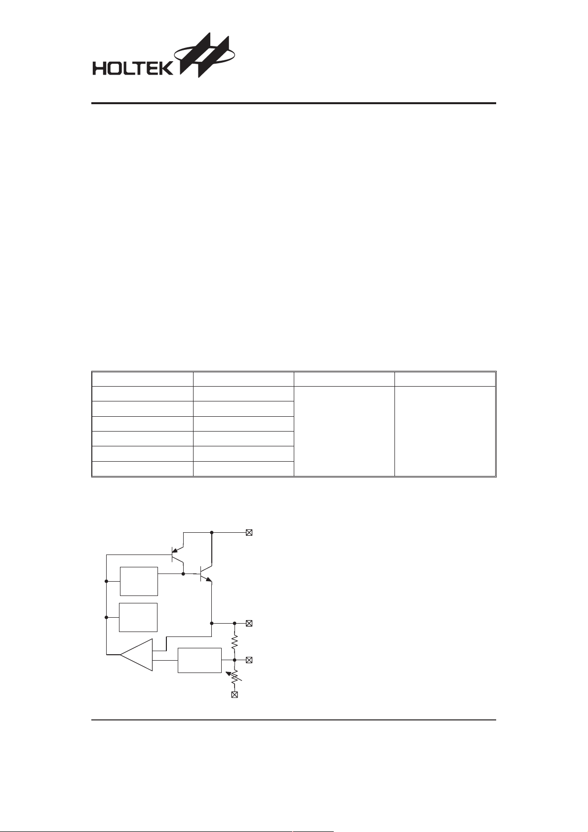
Block Diagram
V
I N
C u r r e n t
L i m i t i n g
A m p l i f i e r
T h e r m a l
P r o t e c t i o n
V
O U T
SOT89
TO92
HT1087-ADJ
HT1087-15
HT1087-18
HT1087-25
HT1087-33
HT1087-50
E r r o r
A m p .
Rev. 1.10 1 October 5, 2007
B a n d g a p
R e f e r e n c e
A D J
G N D
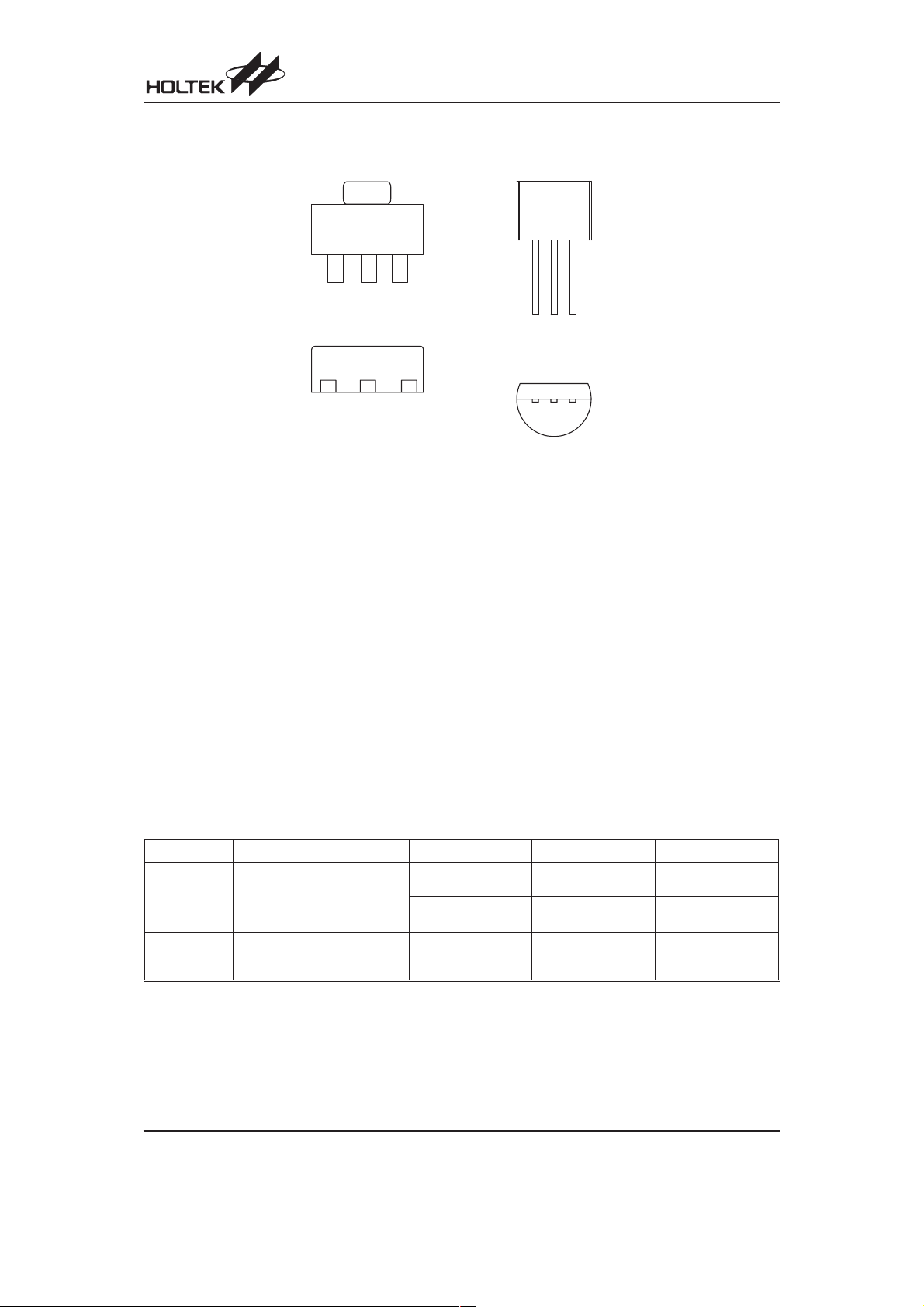
Pin Assignment
HT1087 Series
S O T 8 9
T o p V i e w
V I N
G N D /
A D J
G N D /
A D J
H T 1 0 8 7 - X X
V O U T
V O U T V I N
Absolute Maximum Ratings*
Input Supply Voltage ..................VSS-0.3V to VSS+13V
T O 9 2
H T 1 0 8 7 - X X
V O U T
G N D / A D J
V O U T
G N D / A D J
F r o n t V i e w
V I N
B o t t o m V i e w
V I N
Storage Temperature ...........................-50°Cto125°C
Note: These are stress ratings only. Stresses exceeding the range specified under ²Absolute Maximum Ratings² may
cause substantial damage to the device. Functional operation of this device at other conditions beyond those listed
in the specification is not implied and prolonged exposure to extreme conditions may affect device reliability.
²*² Absolute maximum ratings indicate limits beyond which damage to the device may occur. Operating Ratings indicate conditions for which the device is intended to be functional, but do not guarantee specific performance limits.
The guaranteed specifications apply only for the test conditions listed.
Recommended Operating Conditions
Input Supply Voltage ..................VSS-0.3V to VSS+12V
Ambient Temperature ............................-40°Cto85°C
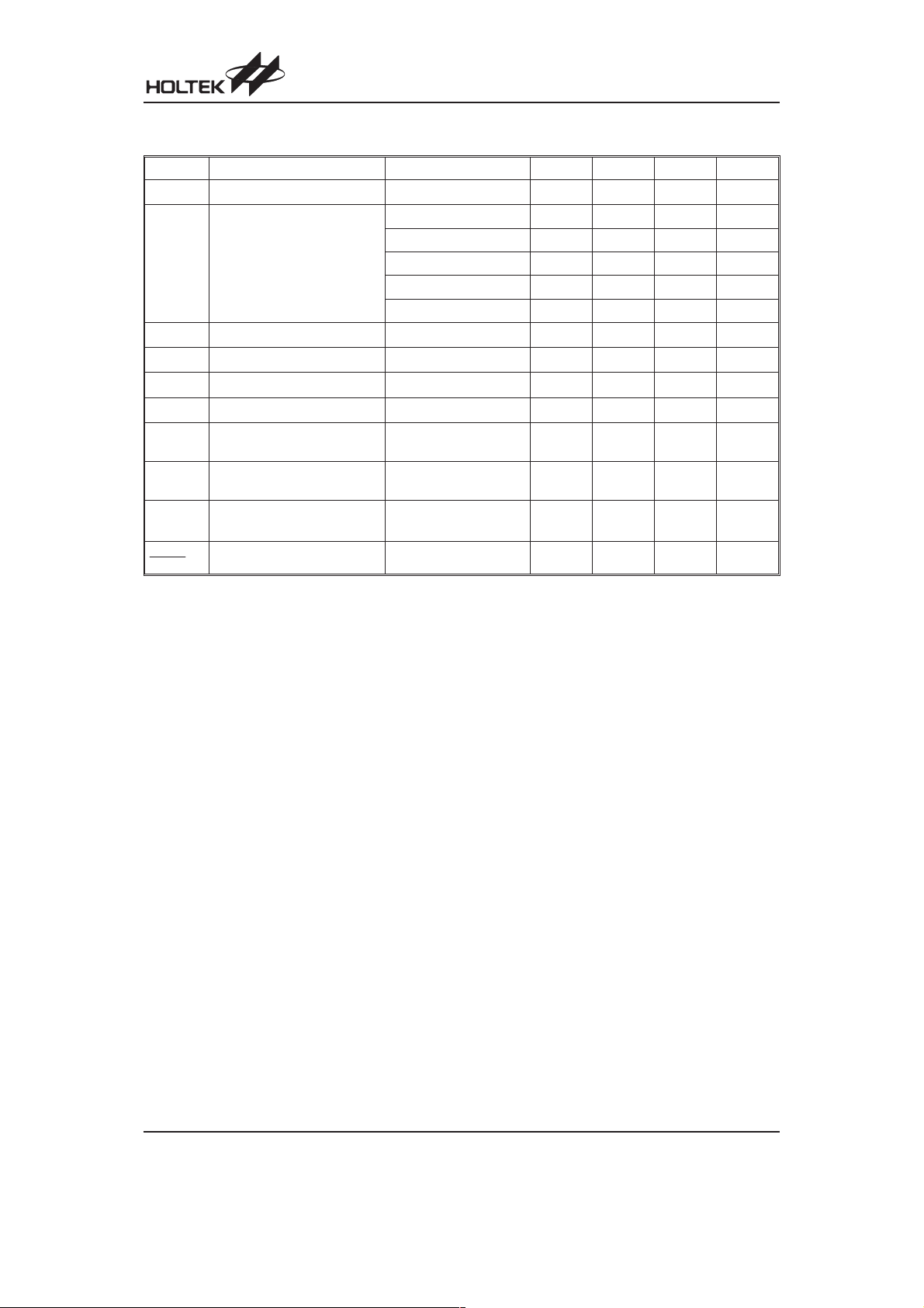
Thermal Information
Symbol Parameter Package Max. Unit
Thermal Resistance
q
JA
(Junction to Ambient)
(Assume no ambient airflow,
no heat sink)
P
D
Power Dissipation
Note: PDis measured at Ta= 25°C
SOT-89
TO-92 200
SOT-89 0.5 W
TO-92 0.5 W
200
°C/W
°C/W
Rev. 1.10 2 October 5, 2007
HT1087 Series
Electrical Characteristics
TJ=25°C, VIN=V
+1.5V, IO=10mA, unless otherwise specified (see note 1)
OUT
Symbol Parameter Test Conditions Min. Typ. Max. Unit
V
REF
Reference Voltage
2.75V £ V
IN
£ 12V
1.225 1.250 1.275 V
HT1087-15 1.470 1.500 1.530 V
HT1087-18 1.764 1.800 1.836 V
V
OUT
Output Voltage
HT1087-25 2.450 2.500 2.550 V
HT1087-33 3.234 3.300 3.366 V
HT1087-50 4.900 5.000 5.100 V
=0.5A
DV
DV
V
I
LIMIT
I
ADJ
I
SS
LOAD
LINE
DIF
Load Regulation (see note 2)
Line Regulation
Dropout Voltage (see note 3)
Current Limit (see note 4)
Adjust Pin Current
(Variable Version)
Quiescent Current
(Fixed Version)
RR Ripple Rejection
V
D
O U T
T
D
Temperature Coefficient
a
I
OUT
2.75V £ V
DV
OUT
DV
OUT
2.75V £ V
2.75V £ V
£ 12V ¾
IN
=2%, I
=0.5A ¾
OUT
=10%
£ 12V
IN
£ 12V
IN
120Hz input ripple
=22mF
C
OUT
-40°C<Ta<85°C ¾±0.4 ¾ mV/°C
1
¾
0.015 0.15 %/V
1.1 1.3 V
0.5 1.5
¾
55 120
¾
¾
60
20 mV
¾
813mA
¾
A
mA
dB
Note:
1. Specifications are production tested at room temperature, Ta. Specifications within the -40°Cto85°C
operating temperature range are assured by design, characterization and correlation withStatistical Quality
Controls (SQC).
2. Loadregulation is measured at a constant junction temperature, using pulse testing with a low ON time and
is guaranteed up to the maximum power dissipation. Power dissipation is determined by the input/output
differential voltage and the output current. Guaranteed maximum power dissipation will notbe available over
the full input/output range. The maximum allowable power dissipation at any ambient temperature is
=(T
P
D
J(MAX)
- Ta ) / qJA.
3. Dropoutvoltage is defined as the input voltage minus the output voltage that produces a 2% change inthe
output voltage from the value at V
IN=VOUT
+1.5V with a fixed load.
4. Current limit is measured by pulsing for a short time.
Rev. 1.10 3 October 5, 2007
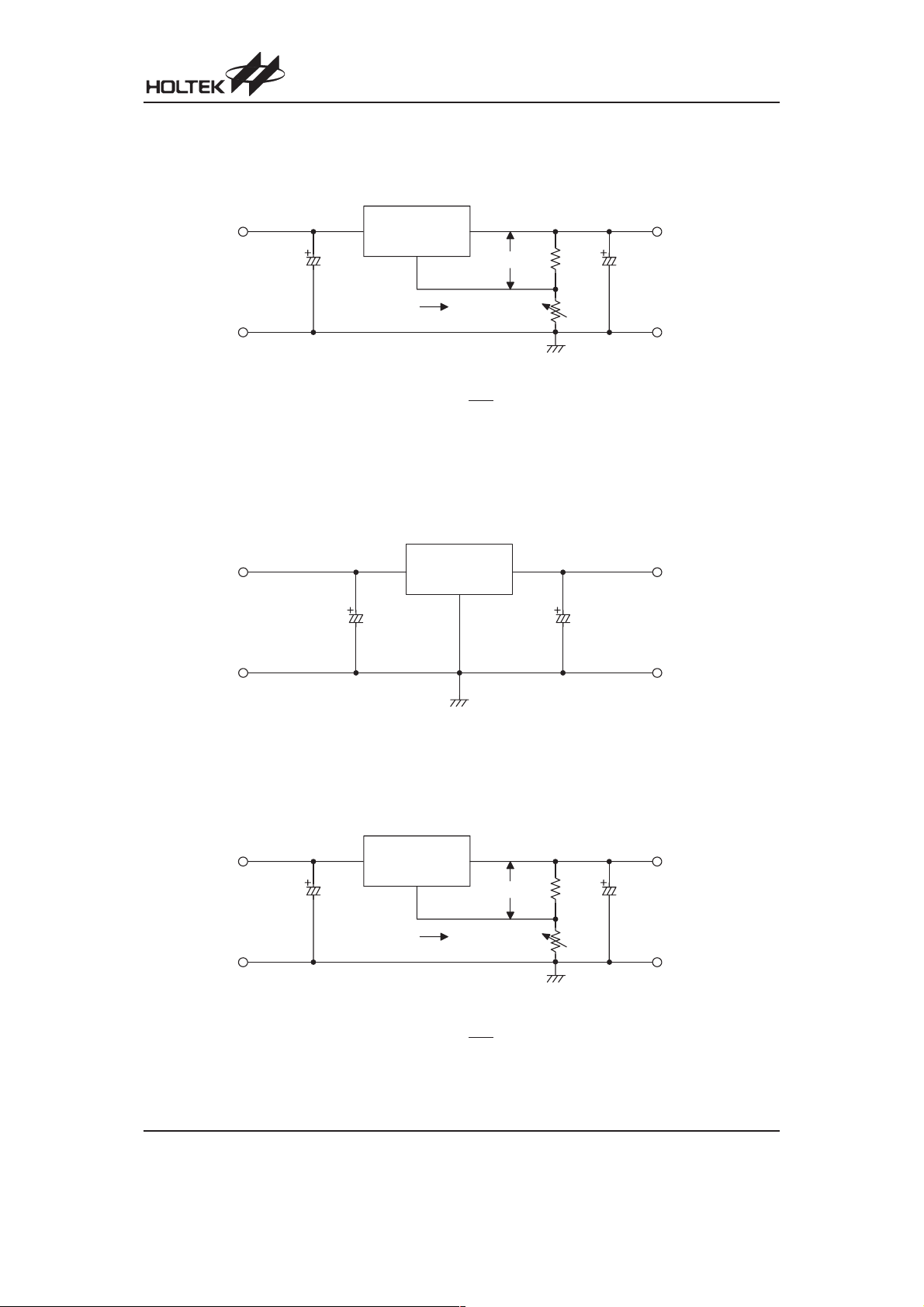
Application Circuits
Basic Circuits
·
Variable voltage type
HT1087 Series
V
I N
C 1
1 0
m
C o m m o n C o m m o n
Note:
C1 isrequired if the needed if the device is located far from filter capacitors, the recommended value is 10mF.
V I N
H T 1 0 8 7 - A D J
F
V=V(1+
OUT REF ADJ
A D J
I
A D J
V O U T
V
R2
)+I R2
R1
R E F
S i n g l e p o i n t G N D
R 1
1 2 5
W
R 2
1 k
W
V
O U T
C 2
1 0
F
m
C2 is required for stability, the recommended value is 10mF.
R1 is required for regulation, the recommended value is 125W.
·
Fixed voltage type
V
I N
V I N
H T 1 0 8 7
V O U T
V
O U T
S e r i e s
C 1
F
1 0
m
G N D
C 2
F
1 0
m
C o m m o n C o m m o n
Note:
C1 isrequired if the needed if the device is located far from filter capacitors, the recommended value is 10mF.
S i n g l e p o i n t G N D
C2 is required for stability, the recommended value is 10mF.
Typical Application Circuits
·
1.25~10.5V regulator
2 . 7 5 V£V
C o m m o n C o m m o n
1 2 V
I N
£
C 1
1 0
m
V I N
H T 1 0 8 7 - A D J
F
V=V(1+
OUT REF ADJ
A D J
I
A D J
V O U T
V
R2
)+I R2
R1
R E F
S i n g l e p o i n t G N D
R 1
1 2 5
W
R 2
1 k
W
V
O U T
C 2
1 0
F
m
Rev. 1.10 4 October 5, 2007

·
Digitally selected outputs
HT1087 Series
V
I N
C 1
1 0
V I N
H T 1 0 8 7 - A D J
F
m
R 2 R 3 R 4 R 5 R n
C o m m o n C o m m o n
N o t e : R 2 c a n s e t t h e m a x i m u m v o l t a g e .
·
High output current positive voltage regulator
T r 1
V
I N
R 1
C 1
1 0
F
m
C o m m o n C o m m o n
V
V O U T
O U T
R 1
1 2 5
A D J
I n p u t s
I
C 1
V I N
H T 1 0 8 7
S e r i e s
V O U T
I
R E G
G N D
W
S i n g l e p o i n t
G N D
C 2
1 0
C 2
1 0
F
m
V
O U T
I
O
F
m
S i n g l e p o i n t G N D
·
Increased Output voltage Circuit
V
I N
C o m m o n C o m m o n
V
=
IO = I
B E 1
I
-
R E G
+ I
C 1
I
C 1
( 1 +b)
R E G
V O U T
,
V
O U T
R
1
V I N
H T 1 0 8 7
S e r i e s
C 1
1 0
F
m
G N D
I
S S
D 1
S i n g l e p o i n t G N D
V=V+V
OUT XX D1
V
XX
R=
1
I
SS
C 2
V
1 0
X X
F
m
R 1
Rev. 1.10 5 October 5, 2007

·
Dual Supply Circuit
HT1087 Series
I C 1
V
I N
I C 2
V I N
H T 1 0 8 7
S e r i e s
C 1
1 0
F
m
G N D
V I N
V O U T
H T 1 0 8 7
S e r i e s
C 2
1 0
F
m
G N D
R 1
V O U T
V
O U T 1
V
X X 1
V
X X 2
C 3
1 0
F
m
V
O U T 2
C o m m o n C o m m o n
·
Tracking Voltage Regulator
V
I N
- V
I N
V I N
C 1
1 0
F
m
S i n g l e p o i n t G N D
S i n g l e p o i n t G N D
V=V+V
OUT1 XX2 XX1
V=V
OUT2 XX2
H T 1 0 8 7
V O U T
S e r i e s
G N D
R
-V = V x
OOUT
A
R
B
V
O U T
C 2
1 0
m
R
F
A
R
B
- V
O
Rev. 1.10 6 October 5, 2007

Package Information
3-Pin SOT89 Outline Dimensions
HT1087 Series
A
B
E
G
F
Symbol
H
Dimensions in mil
Min. Nom. Max.
A 173
B64
C90
D35
E 155
F14
G17
H
¾
I55
J14
I
J
C
D
¾
¾
¾
¾
¾
¾
¾
59
¾
¾
181
72
102
47
167
19
22
¾
63
17
Rev. 1.10 7 October 5, 2007

3-Pin TO92 Outline Dimensions
HT1087 Series
A
B
D
C
E
F
G
H
Symbol
Min. Nom. Max.
A 170
B 170
C 500
D11
E90
F45
G45
H 130
I8
Dimensions in mil
¾
¾
¾¾
¾
¾
¾
¾
¾
¾
a 4°¾6°
200
200
20
110
55
65
160
18
Rev. 1.10 8 October 5, 2007

Product Tape and Reel Specifications
Reel Dimensions
HT1087 Series
T 2
A
B
T 1
D
SOT89
Symbol Description Dimensions in mm
A Reel Outer Diameter
B Reel Inner Diameter
180±1.0
62±1.5
C Spindle Hole Diameter 12.75+0.15
D Key Slit Width
1.9±0.15
T1 Space Between Flange 12.4+0.2
T2 Reel Thickness
17-0.4
C
Rev. 1.10 9 October 5, 2007

TO92 Reel Dimensions (Unit: mm)
HT1087 Series
P a c k a g e U p , F l a t S i d e U p
3 0
P a c k a g e U p , F l a t S i d e D o w n
5 8
8 8
3 6 0
4 3
Rev. 1.10 10 October 5, 2007

Carrier Tape Dimensions
E
HT1087 Series
D
P 1P 0
t
F
PD 1
A 0
W
C
SOT89
Symbol Description Dimensions in mm
W Carrier Tape Width
P Cavity Pitch
E Perforation Position
F Cavity to Perforation (Width Direction)
12.0+0.3
8.0±0.1
1.75±0.1
5.5±0.05
D Perforation Diameter 1.5+0.1
D1 Cavity Hole Diameter 1.5+0.1
P0 Perforation Pitch
P1 Cavity to Perforation (Length Direction)
A0 Cavity Length
B0 Cavity Width
K0 Cavity Depth
t Carrier Tape Thickness
4.0±0.1
2.0±0.10
4.8±0.1
4.5±0.1
1.8±0.1
0.30±0.013
C Cover Tape Width 9.3
B 0
K 0
-0.1
Rev. 1.10 11 October 5, 2007

TO92 Carrier Tape Dimensions
HT1087 Series
P
H 1
H
H 0
F 1 F 2
P 2
P 0
l 1
D 0
TO92
Symbol Description Dimensions in mm
I1 Taped Lead Length (2.5)
P Component Pitch
P
P
F
F
Dh
0
2
1
2
Perforation Pitch
Component to Perforation (Length Direction)
Lead Spread
Lead Spread
Component Alignment
W Carrier Tape Width
W
W
W
H
0
H
1
D
0
Hold-down Tape Width
0
Perforation Position
1
Hold-down Tape Position (0.5)
2
Lead Clinch Height
Component Height Less than 24.7
Perforation Diameter
t Taped Lead Thickness
H Component Base Height
Note:
Thickness less than 0.38±0.05mm~0.5mm
12.7±1.0
12.7±0.3
6.35±0.4
2.5+0.4
2.5+0.4
0±0.1
18.0+1.0
6.0±0.5
9.0±0.5
16.0±0.5
4.0±0.2
0.7±0.2
19.0±0.5
P0 Accumulated pitch tolerance: ±1mm/20pitches.
( ) Bracketed figures are for consultation only
-0.1
-0.1
-0.5
h
D
W 2
W 0
W 1
W
t
Rev. 1.10 12 October 5, 2007

Holtek Semiconductor Inc. (Headquarters)
No.3, Creation Rd. II, Science Park, Hsinchu, Taiwan
Tel: 886-3-563-1999
Fax: 886-3-563-1189
http://www.holtek.com.tw
Holtek Semiconductor Inc. (Taipei Sales Office)
4F-2, No. 3-2, YuanQu St., Nankang Software Park, Taipei 115, Taiwan
Tel: 886-2-2655-7070
Fax: 886-2-2655-7373
Fax: 886-2-2655-7383 (International sales hotline)
HT1087 Series
Holtek Semiconductor Inc. (Shanghai Sales Office)
7th Floor, Building 2, No.889, Yi Shan Rd., Shanghai, China 200233
Tel: 86-21-6485-5560
Fax: 86-21-6485-0313
http://www.holtek.com.cn
Holtek Semiconductor Inc. (Shenzhen Sales Office)
5/F, Unit A, Productivity Building, Cross of Science M 3rd Road and Gaoxin M 2nd Road, Science Park, Nanshan District,
Shenzhen, China 518057
Tel: 86-755-8616-9908, 86-755-8616-9308
Fax: 86-755-8616-9722
Holtek Semiconductor Inc. (Beijing Sales Office)
Suite 1721, Jinyu Tower, A129 West Xuan Wu Men Street, Xicheng District, Beijing, China 100031
Tel: 86-10-6641-0030, 86-10-6641-7751, 86-10-6641-7752
Fax: 86-10-6641-0125
Holtek Semiconductor Inc. (Chengdu Sales Office)
709, Building 3, Champagne Plaza, No.97 Dongda Street, Chengdu, Sichuan, China 610016
Tel: 86-28-6653-6590
Fax: 86-28-6653-6591
Holmate Semiconductor, Inc. (North America Sales Office)
46729 Fremont Blvd., Fremont, CA 94538
Tel: 1-510-252-9880
Fax: 1-510-252-9885
http://www.holmate.com
Copyright Ó 2007 by HOLTEK SEMICONDUCTOR INC.
The information appearing in this Data Sheet is believed to be accurate at the time of publication. However, Holtek as
sumes no responsibility arising from the use of the specifications described. The applications mentioned herein are used
solely for the purpose of illustration and Holtek makes no warranty or representation that such applications will be suitable
without further modification, nor recommends the use of its products for application that may present a risk to human life
due to malfunction or otherwise. Holtek¢s products are not authorized for use as critical components in life support devices
or systems. Holtek reserves the right to alter its products without prior notification. For the most up-to-date information,
please visit our web site at http://www.holtek.com.tw.
-
Rev. 1.10 13 October 5, 2007
 Loading...