

Page 1

ESK32-A2A31 2.8 Inch TFT LCD Module
User Manual
Revision: V1.00 Date: February 02, 2018February 02, 2018
Page 2

Rev. 1.00 2 of 12 February 02, 2018
ESK32-A2A31 2.8 Inch TFT LCD Module
User Manual
Table of Contents
Table of Contents
1 Introduction ............................................................................................................. 5
2 Hardware Layout ..................................................................................................... 5
Communication Interface Switch – SW1 .......................................................................................... 6
Extension Connector – CN2 ............................................................................................................. 6
3 Using the Module .................................................................................................... 7
Tool Preparation ..................................................................................................................... 7
LCD Module Setting ............................................................................................................... 7
Expansion Board Setting ....................................................................................................... 7
Board Assembly ..................................................................................................................... 9
Obtain the Example Program ................................................................................................ 9
Compile and Execute the Program ...................................................................................... 10
4 Schematics ............................................................................................................ 10
2.8 Inches TFT LCD Module – ESK32-A2A31.................................................................................11
Page 3

Rev. 1.00 3 of 12 February 02, 2018
ESK32-A2A31 2.8 Inch TFT LCD Module
User Manual
List of Tables
List of Tables
Table 1. Communication Interface Switch SW1 ........................................................................................ 6
Table 2. Extension Connector CN2 ........................................................................................................... 6
Table 3. Expansion Board EBI Interface Switches .................................................................................... 8
Page 4

Rev. 1.00 4 of 12 February 02, 2018
ESK32-A2A31 2.8 Inch TFT LCD Module
User Manual
List of Figures
List of Figures
Figure 1. TFT LCD Module Layout ........................................................................................................... 5
Figure 2. Extension Connector CN2 ......................................................................................................... 6
Figure 3. LCD Module Communication Interface Setting ......................................................................... 7
Figure 4. LCD Module + Expansion Board + Starter Kit ........................................................................... 9
Figure 5. HT32 Firmware Library Download Web Link ........................................................................... 10
Figure 6. 2.8 Inches TFT LCD Module (ESK32-A2A31) Schematic ........................................................11
Page 5

Rev. 1.00 5 of 12 February 02, 2018
ESK32-A2A31 2.8 Inch TFT LCD Module
User Manual
Introduction
1
Introduction
The ESK32-A2A31 TFT LCD Module is designed for the HT32 series expansion board. It supports
SPI and EBI communication interfaces. The ESK32-A2A31 hardware and software can be used
with the ESK32-20001/ESK32-21001 and the HT32 firmware library, providing users with a
complete development environment with which to learn how to use the EBI and SPI interfaces.
Specications:
▆
Use Himax’s TFT LCD driver IC: HX8347-I (T)
▆
2.8 inch TFT LCD with 65 K colours and 320×240 resolutions
▆
Supports SPI and EBI interfaces
2
Hardware Layout
Figure 1. TFT LCD Module Layout
Page 6

Rev. 1.00 6 of 12 February 02, 2018
ESK32-A2A31 2.8 Inch TFT LCD Module
User Manual
Hardware Layout
Communication Interface Switch – SW1
Table 1. Communication Interface Switch SW1
Switch No.
Description
1 2 3 4
0 0 0 x 8080 MCU 16-bit parallel
1 0 0 x 8080 MCU 8-bit parallel
ID 0 1 x 3-wire serial interface
x 1 1 x 4-wire serial interface
x: Don‘t care
Extension Connector – CN2
Figure 2. Extension Connector CN2
Table 2. Extension Connector CN2
Pin No. Description Pin No. Description
1 VDD5 2 GND
3 BL_EN 4 NC
5 NC 6 WR/SCL
7 MISO 8 MOSI
9 /CS 10 NC
11 NC 12 /Reset
13 GND 14 VDD33
15 PD0 16 PD1
17 PD2 18 PD3
19 PD4 20 PD5
21 PD6 22 PD7
23 PD8 24 PD9
25 PD10 26 PD11
27 PD12 28 PD13
29 PD14 30 PD15
31 PD16 32 PD17
33 /RD 34 RS
Page 7

Rev. 1.00 7 of 12 February 02, 2018
ESK32-A2A31 2.8 Inch TFT LCD Module
User Manual
Using the Module
3
Using the Module
Tool Preparation
Users need to prepare the HT32 Series expansion board (ESK32-2x001) and the Starter Kit
(ESK32-30xxx)
LCD Module Setting
Before adjusting the communication interface using SW1, refer to the following descriptions and
gure 3 for the LCD module setting details.
If the MCU uses the EBI interface to drive the LCD module, the LCD module should be selected to
be in the EBI mode by switching SW1 of the LCD module to “0000” (default setting).
If the MCU uses the SPI interface to drive the LCD module, the LCD module should be selected to
be in the SPI mode by switching SW1 of the LCD module to “0010”.
Figure 3. LCD Module Communication Interface Setting
Expansion Board Setting
The expansion board settings, J1, J2 and J3 are associated with the LCD module, refer to table 3 for
more details. Refer to the “ESK32-2x001 Expansion Board User Manual” for details on using this
expansion board.
J1: This is used to select whether the LCD Backlight is controlled by the MCU I/O pins or not.
When the MCU I/O pins are insufcient, J1 can be switched to the BL_ON position, ensuring
that the LCD Backlight is always on.
J2: This is used for the EBI interface read operation and determines the MCU EBI OE pin is
connected to the nRD pin of the LCD module or not. When the LCD module needs to read back
the registers or display the RAM, J2 should be switched to OE.
J3: If the MCU supports the EBI interface, then J3 should be open, otherwise J3 should be shorted.
Page 8

Rev. 1.00 8 of 12 February 02, 2018
ESK32-A2A31 2.8 Inch TFT LCD Module
User Manual
Using the Module
Table 3. Expansion Board EBI Interface Switches
Jumpers Descriptions
J1
LCD Backlight will always be on
LCD Backlight controlled by I/O pin
J2
The LCD module nRD pin is switched to the EBI OE pin
The LCD module nRD pin is switched to a xed pull high
J3
Short: LCD SPI mode
Open: LCD EBI mode
Page 9

Rev. 1.00 9 of 12 February 02, 2018
ESK32-A2A31 2.8 Inch TFT LCD Module
User Manual
Using the Module
Board Assembly
The HT32 series expansion board (ESK32-2x001) is connected to the Starter Kit and the 2.8 inch
LCD module, as shown in gure 4.
Figure 4. LCD Module + Expansion Board + Starter Kit
Obtain the Example Program
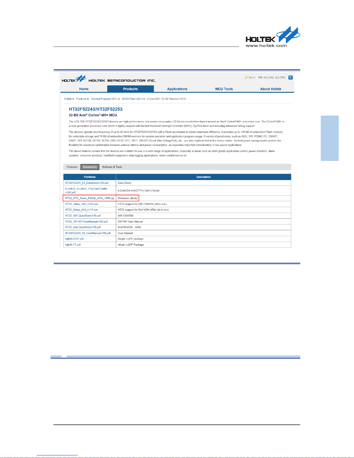
Download the latest Holtek HT32 Firmware Library. The download web link is shown in gure 5.
Unzip the HT32 Firmware Library after downloading.
Page 10
Rev. 1.00 10 of 12 February 02, 2018
ESK32-A2A31 2.8 Inch TFT LCD Module
User Manual
Schematics
Figure 5. HT32 Firmware Library Download Web Link
Compile and Execute the Program
Open the LCD example project:
Keil: \example\LCD\LCD28\MDK_ARMvx\Project_xxxxx.uvprojx
IAR: \example\LCD\LCD28\EWARMvx\Project_xxxxx.eww
Compile and execute the LCD example program after which, “Holtek HT32 Series LCD Example”
will appear on the LCD.
4
Schematics
This section shows the LCD module circuitry.
Page 11

2.8 Inches TFT LCD Module – ESK32-A2A31
Mount only for SPI interfaceMount only for parallel interface
0 0 0 80-System 16-bit
Ⅰ
IM2 IM1 IM0 Interface Mode
0 0 1 80-System 8-bit
Ⅰ
1 0 ID 3-Wire serial
Ⅰ
1 1 X 4-Wire serial
Ⅰ
LED_A
PD0
PD1
PD2
PD3
PD4
PD5
PD6
PD7
PD8
PD9
PD11
PD12
PD13
PD14
PD15
PD16
PD17
SDI
WR/SCL
/RD
/RESET
RS
/CS
WR/SCL
/CS
/RD
RS
EN
/CS
PD0
PD2
PD4
PD6
PD8
PD10
PD12
PD14
PD16
/RD RS
PD17
PD15
PD13
PD11
PD9
PD7
PD5
PD3
PD1
/RESET
WR/SCL
SDISDO
SDO
LED_K1
LED_K2
LED_K3
LED_K4
PD10
PD15
PD14
PD13
PD12
PD11
PD10
PD9
PD8
PD7
PD6
PD5
PD4
PD3
PD2
PD1
PD0
PD16
PD17
LED_A
EN
LED_K1
LED_K2
LED_K3
LED_K4
VDD33
VDD33
VDD33
VDD33
RN1
RP4K7
RN1
RP4K7
182736
45
R3
10K/5%/0603
R3
10K/5%/0603
R8 75/5%/0603R8 75/5%/0603
C3
1uF/0603C31uF/0603
C2 1uF/0603C2 1uF/0603
R1 4K7/0603R1 4K7/0603
R11 75/5%/0603R11 75/5%/0603
R7
4K7/0603R74K7/0603
U1
HT7936U1HT7936
VOUT
1
GND
2
EN3C-
4
VIN
5
C+
6
CN2
LCM HEADER 17X2
CN2
LCM HEADER 17X2
VDD51GND0
2
BL_EN3I2C_SDA
4
I2C_SCL5WR/SCL
6
MISO7MOSI
8
/CS9PENIRQ
10
NC011/RESET
12
GND113VDD33
14
PD0
15
PD1
16
PD2
17
PD3
18
PD4
19
PD5
20
PD6
21
PD7
22
PD8
23
PD9
24
PD1025PD11
26
PD1227PD13
28
PD1429PD15
30
PD1631PD17
32
/RD
33
RS
34
RN2
RP4K7
RN2
RP4K7
182736
45
SW1
SW DIP-4
SW1
SW DIP-4
R10 75/5%/0603R10 75/5%/0603
R9 75/5%/0603R9 75/5%/0603
RN5
RP4K7
RN5
RP4K7
182736
45
C1
1uF/0603C11uF/0603
RN3
RP4K7
RN3
RP4K7
182736
45
R5
4K7/0603R54K7/0603
R4
4K7/0603R44K7/0603
R2 4K7/0603R2 4K7/0603
+
C4
10uF/CASE-A
+
C4
10uF/CASE-A
RN4
RP4K7
RN4
RP4K7
182736
45
CN1
TFT3P4263 /40PIN
CN1
TFT3P4263 /40PIN
LEDA1LEDK12LEDK23LEDK34LEDK45IM06IM17IM28IM39/RESET10DB1711DB1612DB1513DB1414DB1315DB1216DB1117DB1018DB919DB820DB721DB622DB523DB424DB325DB226DB127DB028SDO29SDI30RD31WR/SCL32RS33CS34FMARK35IOVCC36VCC37VCI38GND39NC
40
R6
4K7/0603R64K7/0603
Figure 6. 2.8 Inches TFT LCD Module (ESK32-A2A31) Schematic
Page 12

Rev. 1.00 12 of 12 February 02, 2018
ESK32-A2A31 2.8 Inch TFT LCD Module
User Manual
Schematics
Copyright© 2018 by HOLTEK SEMICONDUCTOR INC.
The information appearing in this Data Sheet is believed to be accurate at the time
of publication. However, Holtek assumes no responsibility arising from the use of
the specifications described. The applications mentioned herein are used solely for
the purpose of illustration and Holtek makes no warranty or representation that such
applications will be suitable without further modification, nor recommends the use of
its products for application that may present a risk to human life due to malfunction or
otherwise. Holtek's products are not authorized for use as critical components in life
support devices or systems. Holtek reserves the right to alter its products without prior
notication. For the most up-to-date information, please visit our web site at http://www.
holtek.com/en/.
 Loading...