

HI-8685,HI-8686
ARINCINTERFACEDEVICE
ARINC429&561SerialDatato16-BitParallelData
DESCRIPTION
TheHI-8685andHI-8686aresystemcomponentsfor
interfacingincomingARINC429signalsto16-bitparallel
datausingproven+5Vanalog/digitalCMOStechnology.
Bothproductsincorporatethedigitallogicandanalogline
receivercircuitryinasingledevice.
ThereceiversontheHI-8685andtheHI-8686connect
directlytotheARINC429Busandtranslatetheincoming
signalstonormalCMOSlevels.Internalcomparatorlevels
aresetjustbelowthestandard6.5voltminimumdata
thresholdandjustabovethestandard2.5voltmaximumnull
threshold.The-10versionoftheHI-8685allowst he
incorporationofanexternal10Kresistanceinserieswith
eachARINCinputforlightningprotectionwithoutaffecting
ARINCleveldetection.
Bothproductsofferhighspeed16-bitparallelbusinterface,
a32-bitbuffer,anderrordetectionforwordlengthandparity.
Aresetpinisalsoprovidedforpower-oninitialization.
Ω
!
!
AutomaticconversionofserialARINC429,575&
561datato16-bitparalleldata
Highspeedparallel16-bitdatabus
Errordetection-and
On-chiplinereceiver
Inputhysteresisofatleast2volts
Testlnputsbypassanaloginputs
Simplifiedlightningprotectionwiththeabilitytoadd
10Kohmexternalseriesresistors
Small,packageoptions:
SOIC,TQFPandPLCC
Militaryprocessingavailable
!
!
!
!
!
!
!
!
wordlengthparity
Resetinputforpower-oninitialization
surfacemount,plastic
FEATURES
PINCONFIGURATIONS (TopView)
February2001
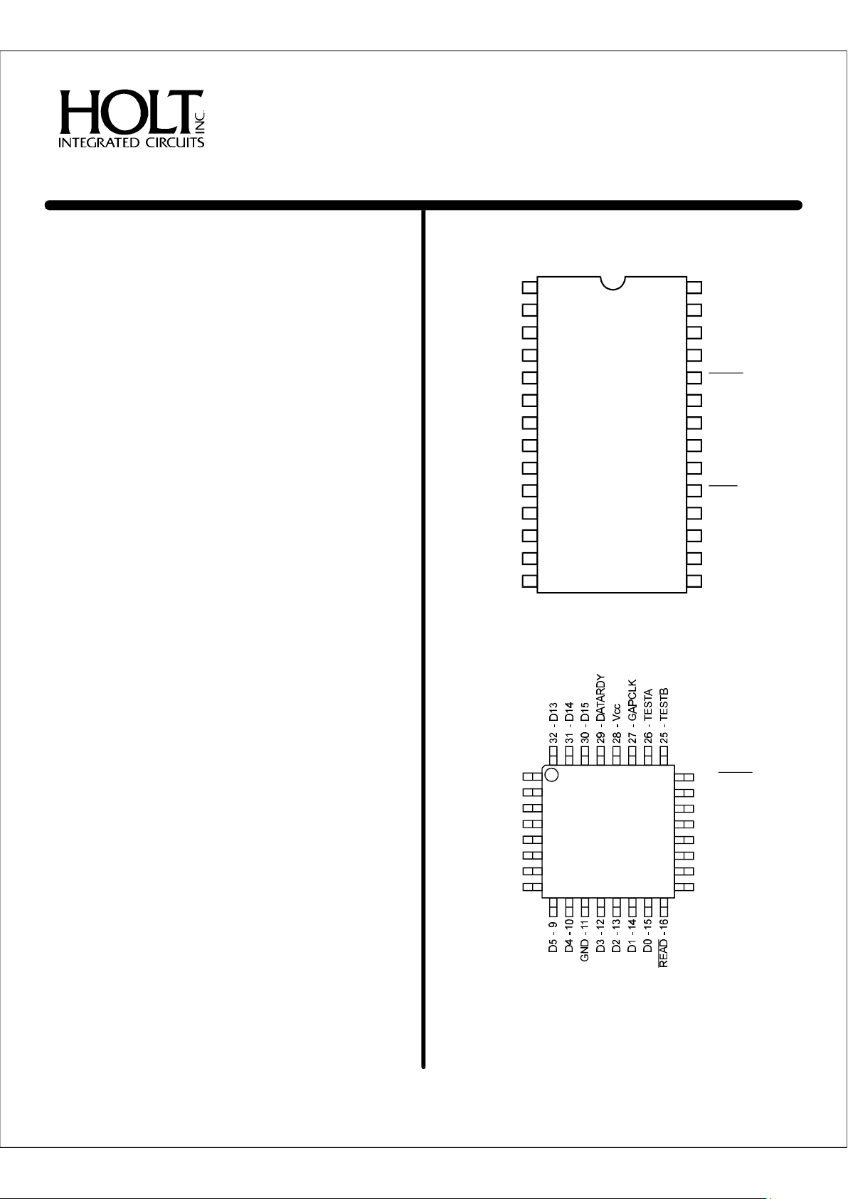
HI-8685
28-PinPlasticSOIC-WBPackage
HI-8686
32-PinPlasticTQFPPackage
HI-8686PQI
HI-8686PQT
2423-RINB-10
22-RINB
21-RINA
20-RINA-10
19-ERROR
18-PARITYENB
17-N/C
RESET
HI-8685PSI
HI-8685PST
&
HI-8685PSI-10
HI-8685PST-10
DATARDY
D15
D14
D13
D12
D11
D10
D9
D8
D7
D6
D5
D4
GND
Vcc
GAPCLK
TESTA
TESTB
RINB(-10)
RINA(-10)
ERROR
PARITYENB
D0
D1
D2
D3
RESET
READ
28
27
26
25
24
23
22
21
20
19
18
17
16
15
1
2
3
4
5
6
7
8
9
10
11
12
13
14
N/C-1
D12-2
D11-3
D10-4
D9-5
D8-6
D7-7
D6-8
HOLTINTEGRATEDCIRCUITS
1(DS8685Rev.G)02/01
(Seepage8foradditionalpinconfigurations)
HI-8685,HI-8686
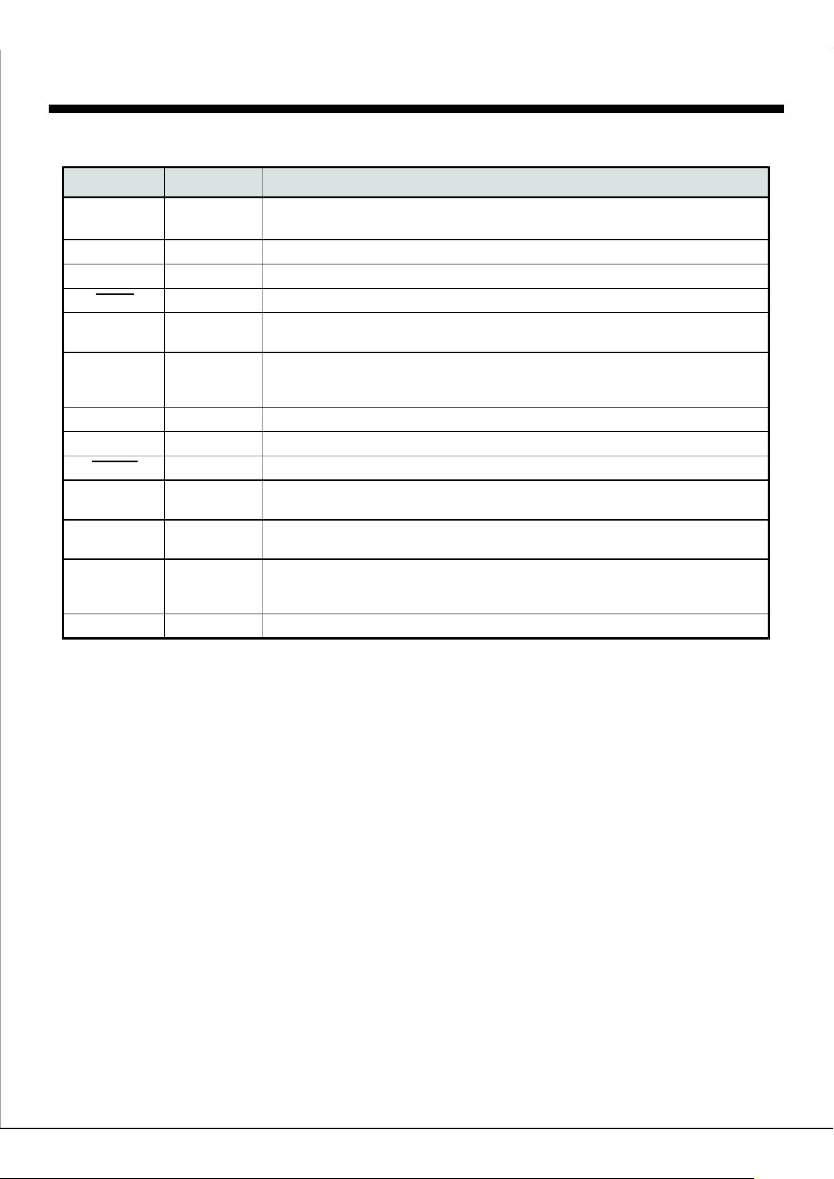
PINDESCRIPTIONS
DATARDYOUTPUTReceiverdatareadyflag.Ahighlevelindicatesdataisavailableinthereceive
buffer.Flaggoeslowwhenthefirst16-bitbyteisread.
D0toD15OUTPUT16-bitparalleldatabus(tri-state)
GNDPOWER0V
INPUTReadstrobe.Alowleveltransfersreceivebufferdatatothedatabus
PARITYENBINPUTParityEnable-Ahighlevelactivatesoddparitycheckingwhichreplacesthe
32ndARINCbitwithanerrorbit.Otherwise,the32ndARINCbitisunchanged
ERROROUTPUTErrorFlag.Ahighlevelindicatesabitcounterror(numberofARINCbitswas
lessthanorgreaterthan32)and/oraparity errorifparitydetectionwasenabled
(PARITYENBhigh)
RINA/RINA-10INPUTPositivedirectARINCserialdatainput
RINB/RINB-10INPUTNegativedirectARINCserialdatainput(bothRINBandRINB-10onHI-8686)
INPUTInternallogicstatesareinitializedwithalowlevel
TESTAINPUTUsedinconjunctionwiththeTESTBinputtobypassthebuilt-inanalogline
receivercircuitry
TESTBINPUTU
GAPCLKINPUTGapClock.DeterminestheminimumtimerequiredbetweenARINCwordsfor
detection.Theminimumwordgaptimeisbetween16and17clockcyclesof
thissignal.
VccPOWER+5V±10%supply
SIGNALFUNCTIONDESCRIPTION
READ
RESET
(bothRINAandRINA-10onHI-8686)
sedinconjunctionwiththeTESTAinputtobypassthebuilt-inanalogline
receivercircuitry
FUNCTIONALDESCRIPTION
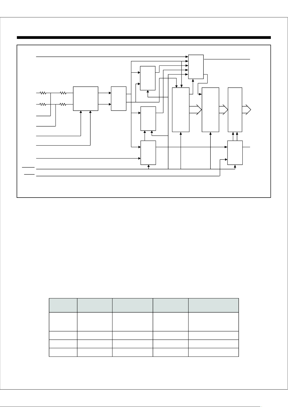
TheHI-8685andHI-8686areserialto16-bitparallelconverters.Theincomingdatastreamisseriallyshiftedintoaninput
register,checkedforerrors,andthentransferredinparallelto
a32-bitreceivebuffer.Thereceivedatacanbeaccessedusingtwo16-bitparallelreadoperationswhilethenextserial
datasteamisbeingreceived.
TheblockdiagramforboththeHI-8685andHI-8685-10productsisfoundinFigure1.Bothhavebuilt-inreceiverseliminatingtheneedforadditionalexternalARINCleveldetection
circuitry.Theonlydifferencebetweenthetwoproductsisthe
am ountofinternalresistanceinserieswitheachARINCinput.
Typically35KresistorsareinserieswithboththeRINAand
RINBARINC429inputs.Theyconnecttoleveltranslators
whoseresistancetoGNDistypically10KAfterleveltrans-
RECEIVERINPUTS
HI-8685ARINCINPUTS(RINA&RINB)
Ω
Ω.
lation,thebufferedinputsdriveadifferentialamplifier.The
differentialsignaliscomparedtolevelsderivedfromadivider
betweenVCCandGND.Thenominalsettingscorrespondto
aOne/Zeroamplitudeof6.0VandaNullamplitudeof3.3V.A
validARINCOne/ZeroinputsetsalatchandaNullinputresetsthelatch.
Sinceanyaddedexternalseriesresistancewillaffectthevoltagetranslation,theHI-8685-10producthasonly25Kof
the35KseriesresistancerequiredforproperARINC429
leveldetection.Theremaining10Krequiredisavailableto
theuserforincorporationinexterna lcircuitrysuchasfor
lightningprotection.
TheHI-8686hasbothsetsofARINCinputs,RINA/RINA-10
andRINB/RINB-10availabletotheuser.
HI-8685-10ARINCINPUTS(RINA-10&RINB-10)
HI-8686ARINCINPUTS
Ω
Ω
Ω
HOLTINTEGRATEDCIRCUITS
2
HI-8685,HI-8686
PROTOCOLDETECTION
TheARINCclockandOne/Zerodatathatarederivedfrom
theoutputsofthebuilt-inlinereceiverisillustratedin
Figure3.Theresultingsteamofdigitaldataisshiftedintoa
32-bitinputregister.
TheARINCclockandOne/Zerodatacanalsobecreated
fromtheTESTAandTESTBinputsasshowninFigure4.
Wheneithertestinputishigh,thebuilt-inanaloglinedriver
isdisabled.
digital
ForARINC561operation,theTESTAandTESTBdigitalinputdatastreamsmustbederivedfromtheARINC561data,
clockandsyncwithexternallogic.
GAPDETECTION
Theendofadatawordisdetectedbyaninternalcounter
thattimesoutwhenadataOneorZeroisnotreceivedfora
periodequalto16cyclesoftheGAPCLKsignal.Thegap
detectiontimemayvarybetween16and17cyclesofthe
GAPCLKsignalsincetheincomingdataandGAPCLKare
notusuallysynchronousinputs.Therequiredfrequencyof
GAPCLKisafunctionofthemininumgaptimespecifiedfor
thetypeofARINCdatabeingreceived.Table1indicates
typicalfrequenciesthatmaybeusedforthevariousdata
ratesnormallyencountered.
BIT
COUNT
PARITY
DETECT
GAP
DETECT
32-BIT
SHIFT
REG.
32-BIT
RECEIVE
BUFFER
32-BIT
TO
16-BIT
MUX
ERROR
DETECT
CLOCK
&
DATA
DETECT
PARITY
ENB
RINB
TESTA
TESTB
GAPCLK
RESET
BYTE
COUNT
READ
DATARDY
ERROR
32 16
32
Figure1.BlockDiagram
ESD
PROTECTION
&
LINE
RECEIVER
DATABUSBITPERIODMINIMUMGAPGAPCLOCKGAPDETECTION
TYPE(s)(s)MHzTIME(s)µµµ
42910450.7521.3-22.7
1.016-17
1.510.7-11.3
42969-133310-5990.1160-170
57569-133310-5990.1160-170
56169-133103-2000.280-85
Table1-TypicalGapDetectionTimes
FUNCTIONALDESCRIPTION(cont.)
RXA
RXB
10K Ω
BIT32
BIT32
RINA
10K Ω
D0-D15
25K Ω
25K Ω
RINB-10
RINA-10
DATA
CLK
HOLTINTEGRATEDCIRCUITS
3
 Loading...