

HI-8685,HI-8686
ARINCINTERFACEDEVICE
ARINC429&561SerialDatato16-BitParallelData
DESCRIPTION
TheHI-8685andHI-8686aresystemcomponentsfor
interfacingincomingARINC429signalsto16-bitparallel
datausingproven+5Vanalog/digitalCMOStechnology.
Bothproductsincorporatethedigitallogicandanalogline
receivercircuitryinasingledevice.
ThereceiversontheHI-8685andtheHI-8686connect
directlytotheARINC429Busandtranslatetheincoming
signalstonormalCMOSlevels.Internalcomparatorlevels
aresetjustbelowthestandard6.5voltminimumdata
thresholdandjustabovethestandard2.5voltmaximumnull
threshold.The-10versionoftheHI-8685allowst he
incorporationofanexternal10Kresistanceinserieswith
eachARINCinputforlightningprotectionwithoutaffecting
ARINCleveldetection.
Bothproductsofferhighspeed16-bitparallelbusinterface,
a32-bitbuffer,anderrordetectionforwordlengthandparity.
Aresetpinisalsoprovidedforpower-oninitialization.
Ω
!
!
AutomaticconversionofserialARINC429,575&
561datato16-bitparalleldata
Highspeedparallel16-bitdatabus
Errordetection-and
On-chiplinereceiver
Inputhysteresisofatleast2volts
Testlnputsbypassanaloginputs
Simplifiedlightningprotectionwiththeabilitytoadd
10Kohmexternalseriesresistors
Small,packageoptions:
SOIC,TQFPandPLCC
Militaryprocessingavailable
!
!
!
!
!
!
!
!
wordlengthparity
Resetinputforpower-oninitialization
surfacemount,plastic
FEATURES
PINCONFIGURATIONS (TopView)
February2001
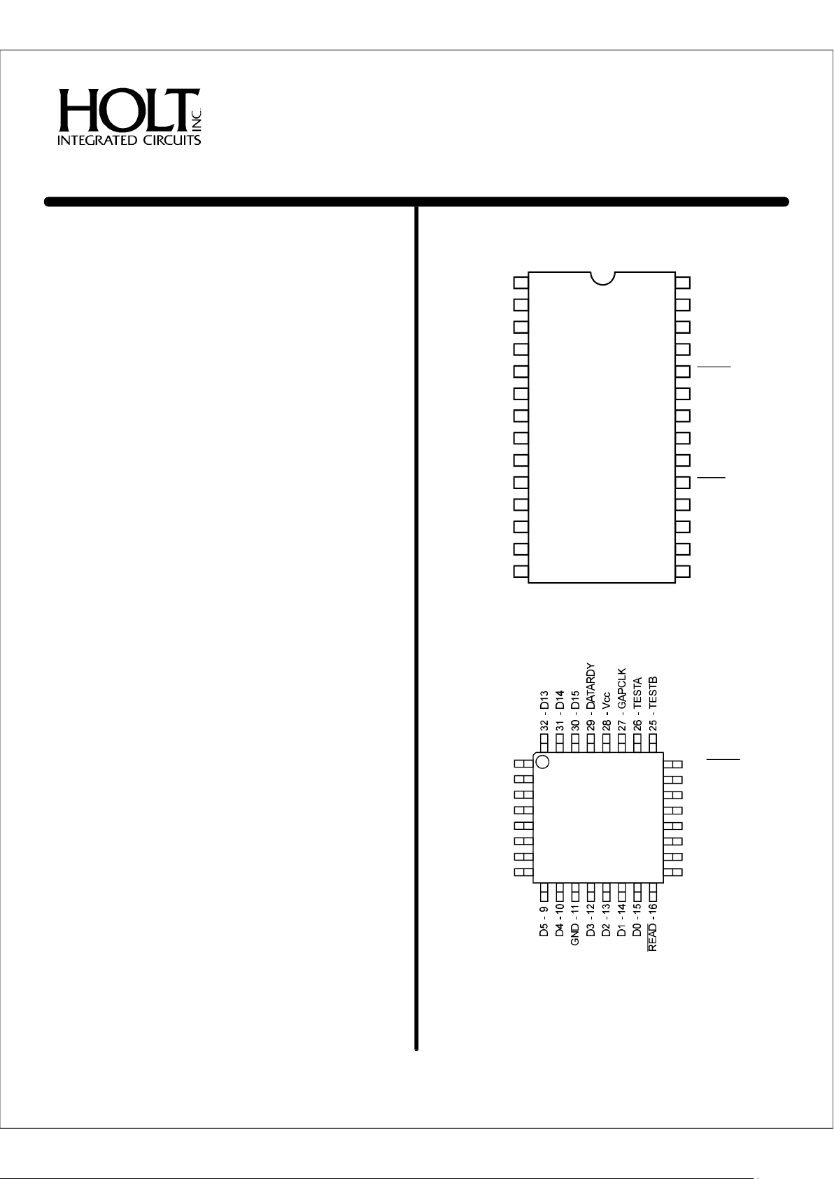
HI-8685
28-PinPlasticSOIC-WBPackage
HI-8686
32-PinPlasticTQFPPackage
HI-8686PQI
HI-8686PQT
2423-RINB-10
22-RINB
21-RINA
20-RINA-10
19-ERROR
18-PARITYENB
17-N/C
RESET
HI-8685PSI
HI-8685PST
&
HI-8685PSI-10
HI-8685PST-10
DATARDY
D15
D14
D13
D12
D11
D10
D9
D8
D7
D6
D5
D4
GND
Vcc
GAPCLK
TESTA
TESTB
RINB(-10)
RINA(-10)
ERROR
PARITYENB
D0
D1
D2
D3
RESET
READ
28
27
26
25
24
23
22
21
20
19
18
17
16
15
1
2
3
4
5
6
7
8
9
10
11
12
13
14
N/C-1
D12-2
D11-3
D10-4
D9-5
D8-6
D7-7
D6-8
HOLTINTEGRATEDCIRCUITS
1(DS8685Rev.G)02/01
(Seepage8foradditionalpinconfigurations)
HI-8685,HI-8686
PINDESCRIPTIONS
DATARDYOUTPUTReceiverdatareadyflag.Ahighlevelindicatesdataisavailableinthereceive
buffer.Flaggoeslowwhenthefirst16-bitbyteisread.
D0toD15OUTPUT16-bitparalleldatabus(tri-state)
GNDPOWER0V
INPUTReadstrobe.Alowleveltransfersreceivebufferdatatothedatabus
PARITYENBINPUTParityEnable-Ahighlevelactivatesoddparitycheckingwhichreplacesthe
32ndARINCbitwithanerrorbit.Otherwise,the32ndARINCbitisunchanged
ERROROUTPUTErrorFlag.Ahighlevelindicatesabitcounterror(numberofARINCbitswas
lessthanorgreaterthan32)and/oraparity errorifparitydetectionwasenabled
(PARITYENBhigh)
RINA/RINA-10INPUTPositivedirectARINCserialdatainput
RINB/RINB-10INPUTNegativedirectARINCserialdatainput(bothRINBandRINB-10onHI-8686)
INPUTInternallogicstatesareinitializedwithalowlevel
TESTAINPUTUsedinconjunctionwiththeTESTBinputtobypassthebuilt-inanalogline
receivercircuitry
TESTBINPUTU
GAPCLKINPUTGapClock.DeterminestheminimumtimerequiredbetweenARINCwordsfor
detection.Theminimumwordgaptimeisbetween16and17clockcyclesof
thissignal.
VccPOWER+5V±10%supply
SIGNALFUNCTIONDESCRIPTION
READ
RESET
(bothRINAandRINA-10onHI-8686)
sedinconjunctionwiththeTESTAinputtobypassthebuilt-inanalogline
receivercircuitry
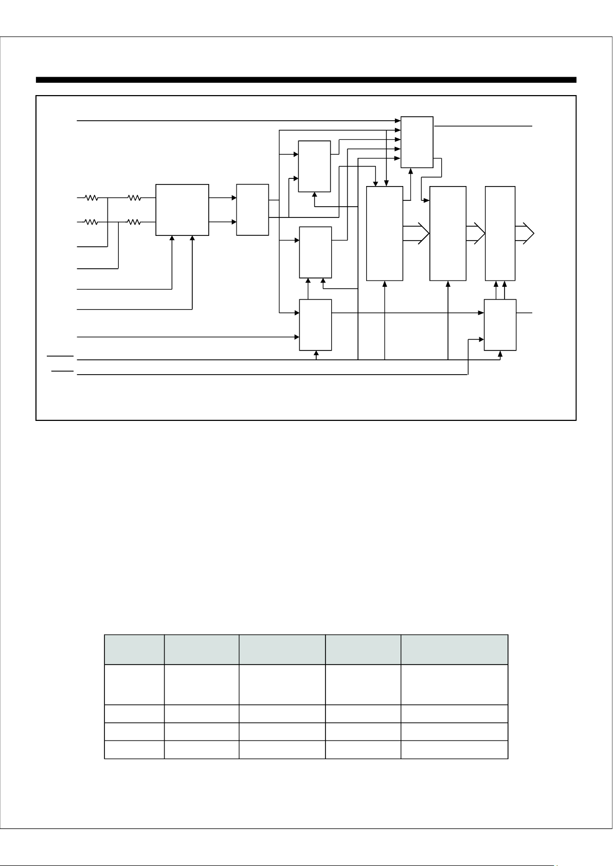
FUNCTIONALDESCRIPTION
TheHI-8685andHI-8686areserialto16-bitparallelconverters.Theincomingdatastreamisseriallyshiftedintoaninput
register,checkedforerrors,andthentransferredinparallelto
a32-bitreceivebuffer.Thereceivedatacanbeaccessedusingtwo16-bitparallelreadoperationswhilethenextserial
datasteamisbeingreceived.
TheblockdiagramforboththeHI-8685andHI-8685-10productsisfoundinFigure1.Bothhavebuilt-inreceiverseliminatingtheneedforadditionalexternalARINCleveldetection
circuitry.Theonlydifferencebetweenthetwoproductsisthe
am ountofinternalresistanceinserieswitheachARINCinput.
Typically35KresistorsareinserieswithboththeRINAand
RINBARINC429inputs.Theyconnecttoleveltranslators
whoseresistancetoGNDistypically10KAfterleveltrans-
RECEIVERINPUTS
HI-8685ARINCINPUTS(RINA&RINB)
Ω
Ω.
lation,thebufferedinputsdriveadifferentialamplifier.The
differentialsignaliscomparedtolevelsderivedfromadivider
betweenVCCandGND.Thenominalsettingscorrespondto
aOne/Zeroamplitudeof6.0VandaNullamplitudeof3.3V.A
validARINCOne/ZeroinputsetsalatchandaNullinputresetsthelatch.
Sinceanyaddedexternalseriesresistancewillaffectthevoltagetranslation,theHI-8685-10producthasonly25Kof
the35KseriesresistancerequiredforproperARINC429
leveldetection.Theremaining10Krequiredisavailableto
theuserforincorporationinexterna lcircuitrysuchasfor
lightningprotection.
TheHI-8686hasbothsetsofARINCinputs,RINA/RINA-10
andRINB/RINB-10availabletotheuser.
HI-8685-10ARINCINPUTS(RINA-10&RINB-10)
HI-8686ARINCINPUTS
Ω
Ω
Ω
HOLTINTEGRATEDCIRCUITS
2
HI-8685,HI-8686
PROTOCOLDETECTION
TheARINCclockandOne/Zerodatathatarederivedfrom
theoutputsofthebuilt-inlinereceiverisillustratedin
Figure3.Theresultingsteamofdigitaldataisshiftedintoa
32-bitinputregister.
TheARINCclockandOne/Zerodatacanalsobecreated
fromtheTESTAandTESTBinputsasshowninFigure4.
Wheneithertestinputishigh,thebuilt-inanaloglinedriver
isdisabled.
digital
ForARINC561operation,theTESTAandTESTBdigitalinputdatastreamsmustbederivedfromtheARINC561data,
clockandsyncwithexternallogic.
GAPDETECTION
Theendofadatawordisdetectedbyaninternalcounter
thattimesoutwhenadataOneorZeroisnotreceivedfora
periodequalto16cyclesoftheGAPCLKsignal.Thegap
detectiontimemayvarybetween16and17cyclesofthe
GAPCLKsignalsincetheincomingdataandGAPCLKare
notusuallysynchronousinputs.Therequiredfrequencyof
GAPCLKisafunctionofthemininumgaptimespecifiedfor
thetypeofARINCdatabeingreceived.Table1indicates
typicalfrequenciesthatmaybeusedforthevariousdata
ratesnormallyencountered.
BIT
COUNT
PARITY
DETECT
GAP
DETECT
32-BIT
SHIFT
REG.
32-BIT
RECEIVE
BUFFER
32-BIT
TO
16-BIT
MUX
ERROR
DETECT
CLOCK
&
DATA
DETECT
PARITY
ENB
RINB
TESTA
TESTB
GAPCLK
RESET
BYTE
COUNT
READ
DATARDY
ERROR
32 16
32
Figure1.BlockDiagram
ESD
PROTECTION
&
LINE
RECEIVER
DATABUSBITPERIODMINIMUMGAPGAPCLOCKGAPDETECTION
TYPE(s)(s)MHzTIME(s)µµµ
42910450.7521.3-22.7
1.016-17
1.510.7-11.3
42969-133310-5990.1160-170
57569-133310-5990.1160-170
56169-133103-2000.280-85
Table1-TypicalGapDetectionTimes
FUNCTIONALDESCRIPTION(cont.)
RXA
RXB
10K Ω
BIT32
BIT32
RINA
10K Ω
D0-D15
25K Ω
25K Ω
RINB-10
RINA-10
DATA
CLK
HOLTINTEGRATEDCIRCUITS
3
HI-8685,HI-8686
Onceawordgapisdetected,thedatawordintheinputregisteristransferredtothereceivebufferandcheckedforerrors.
Whenparitydetectionisenabled(PARITYENBhigh),the
receivedwordischeckedforoddparity.Ifthereisaparity
error,the32ndbitofthereceiveddatawordissethigh.
Ifparitycheckingisdisabled(PARITYENBlow)the32nd
bitofthedatawordisalwaysthe32ndARINCbitreceived.
TheERRORflagoutputissethighuponreceiptofaword
gapandthenumberofbitsreceivedsincetheprevious
wordgapislessthanorgreaterthan32.TheERRORflag
isresetlowwhenthenext validARINCwordiswritteninto
thereceivebufferorwhenispulsedlow.
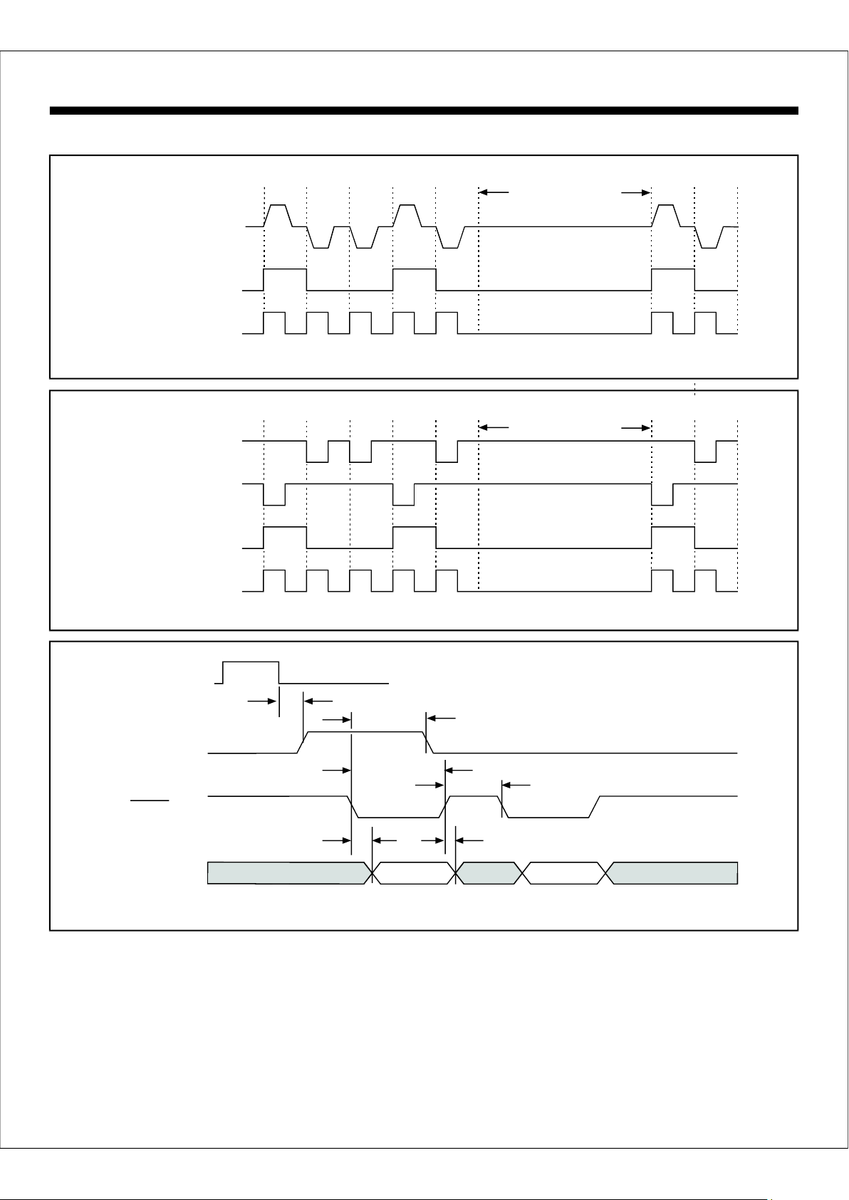
Whenthedatawordistransferredtothereceivebuffer,the
DATARDYpingoeshigh.Thedatawordcanthenberead
intwo16-bitbytesbypulsingtheinputlowasindicatedinFigure5.ThefirstreadcycleresetsDATARDY
lowandincrementsaninternalcountertothesecond
16-bitbyte.Therelationshipbetweeneachbitofan
ARINCwordreceivedandeachbitofthetwo16-bitdata
busbytesisspecifiedinFigure2.
WhenanewARINCwordisreceiveditalwaysoverwrites
thereceivebuffer.Ifthefirstbyteofthepreviouswordhas
notbeenread,thenpreviousdataislostandthereceive
bufferwillcontainthenewARINCword.However,ifthe
DATARDYpingoeshighbetweenthereadingofthefirst
andsecondbytes,thefirstbyteisnolongervalidbecause
thecorrespondingsecondbytehasbeenoverwrittenby
thenewARINCword.Also,thenextreadwillbeofthefirst
byteofthenewARINCwordsincetheinternalbytecounter
isalwaysresettothefirstbytewhennewdataistransferredtothereceivebuffer.
ERRORCHECKING
READINGRECEIVEBUFFER
RESET
READ
FUNCTIONALDESCRIPTION(cont.)
TRUTHTABLE1.
RINA(-10)RINB(-10)TESTATESTBRXARXB
-1.50Vto+1.50V-1.50Vto+1.50V0000
-3.25Vto-6.50V+3.25Vto+6.50V0001
+3.25Vto+6.50V-3.25Vto-6.50V0010
XX0101
XX1010
XX1100
X=don'tcare
ReadByteDataBusBitsARINCBits
1stByte1D0-D15ARINC1-ARINC16
2ndByte2D0-D15ARINC17-ARINC32
FIGURE2.ORDEROFRECEIVEDDATA
RESET
TESTMODE
Alowontheinputsetsaflip-flopwhichinitializesthe
internallogic.Whengoeshigh,theinternallogicremainsintheinitializedstateuntilthefirstwordgapisdetectedpreventingreceptionofapartialword.
Thebuilt-indifferentiallinereceivercanbedisabledallowing
thedataandclockdetectioncircuitrytobedrivendirectly
withdigitalsignals.ThelogicalORfunctionoftheTESTA
andTESTBisdefinedinTruthTable1.Thetwoinputscan
beusedfortestingthereceiverlogicandforinputtingARINC
429typedataderivedfromanothersource/protocol.See
Figure4fortypi caltestinputtiming.
Thedeviceshouldalwaysbeinitializedwithimmediatelyafterenteringthetestmodetoclearapartialword
thatmayhavebeenreceivedsincethelastwordgap.Otherwise,anERRORconditionmayoccurandthefirst32bits
ofdataonthetestinputsmaynotbeproperlyreceived.
Also,whenenteringthetestmode,bothTESTAandTESTB
shouldbesethighandheldinthatstateforatleastone
wordgapperiod(17gapclocks)aftergoeshigh.
Whenexitingthetestmode,bothtestinputsshouldbeheld
lowandthedeviceinitializedwith
RESET
RESET
RESET
RESET
RESET.
HOLTINTEGRATEDCIRCUITS
4
HI-8685,HI-8686
ARINCDataBitsWordGap
2829303132124BitPeriodsMin.
VDIFF
RINA-RINB
0V
+10V
-10V
FIGURE3-RECEIVERINPUTTIMINGFORARINC429
DERIVEDDATA
DERIVEDCLOCK
ARINCDataBitsWordGap
2829303132124BitPeriodsMin.
TESTA
+5V
0V
TESTB
0V
+5V
DERIVEDCLOCK
DERIVEDDATA
FIGURE5-RECEIVERPARALLELDATABUSTIMING
DATARDY
READ
D0-D15
VALID
t
RDYCLR
t
RDPW
t
RR
t
FD
t
RD
VALID
1st16-bits 2nd16-bits
t
DRDY
DERIVEDDATA
TIMINGDIAGRAMS
FIGURE4-TESTINPUTTIMINGFORARINC429
32nd
ARINCbit
HOLTINTEGRATEDCIRCUITS
5

PARAMETERSSYMBOLTESTCONDITIONSMINTYPMAXUNITS
ARINCBusInputs (RINA,RINB,RINA-10&RINB-10)
Differentialinputvoltage
oneorzeroVdifferentialvoltage6.510.013.0volts
nullV""""--2.75volts
commonmodeVwithrespecttoGND--5.0volts
Inputresistance
RINA(-10)toRINB(-10)Rsuppliesfloating3075-Kohm
RINA(-10)orRINB(-10)toGNDorVR"""'1940-Kohm
Inputcapacitance(Guaranteedbutnottested)
differentialCRINA(-10)toRINB(-10)--20pF
toGNDC--20pF
toVC--20pF
DIN
NIN
COM
DIFF
CCSUP
DIFF
G
CCH
SupplyVoltages
V.................................................+5V
TemperatureRange
IndustrialScreening..............-40°Cto+85°C
Hi-TempScreening..............-55°Cto+125°C
MilitaryScreening..................-55°Cto+125°C
JunctionTemperature,Tj....................175°C
CC ±10%
≤+
AllvoltagesreferencedtoGND
Supplyvoltages
V.......................................................+7.0V
Voltageoninputs
RINA(-10)toRINB(-10).........+29Vto-29V
Allotherinputpins..................-0.3toVcc+0.3
DCcurrentperinputpin.......................+10mA
Powerdissipationat25°C
plastic28-pinSO.....1.8W,derate14.1mW/°C
plastic28-pinPLCC.2.3
plastic32-pinSO......1.6
SolderTemperature
Leads.............................+280°Cfor10sec
Packagebody..................................+220°C
StorageTemperature........ .....-65°Cto+150°C
CC
W,derate18.2mW/°C
W,derate15.4mW/°C
NOTE:Stressesaboveabsolutemaximum
ratingsoroutsiderecommendedoperating
conditionsmaycausepermanentdamageto
thedevice.Thesearestressratingsonly.
Operationatthelimitsisnotrecommended.
ABSOLUTEMAXIMUMRATINGS
RECOMMENDEDOPERATINGCONDITIONS
Vcc=5V,GND=0V,TA=OperatingTemperatureRange(unlessotherwisespecified).
DCELECTRICALCHARACTERISTICS
HI-8685,HI-8686
HOLTINTEGRATEDCIRCUITS
6

Vcc=5V,GND=0V,TA=OperatingTemperatureRange(unlessotherwisespecified).
HI-8685,HI-8686
DCELECTRICALCHARACTERISTICS(cont.)
PARAMETERSSYMBOLTESTCONDITIONSMINTYPMAXUNITS
DigitalInputs
Outputs
OperatingSupplyCurrent
(,GAPCLK,,PARITYENA,TESTA&TESTB)
Inputvoltage
highV2.0-V
lowV0.0-0.8volts
Inputcurrent
source--1.0
sink-1.0--
InputcapacitanceC--8.0pF
(D0toD15,ERROR&DATARDY)
Outputvoltage
high
lowI=1.6mA--0.4volts
Outputtri-statecurrent(D0-D15only)
V=5.0V--1.0A
V=0.0V-1.0--
Outputcapacitance--15pF
VIV=0.0V,outputsopen--6.5mA
RESETREAD
IHCC
IL
I
OL
OH
OL
CCCCIN
µ
volts
IV=5.0VA
IV=0.0VA
VI=-1.0mA2.7--volts
V
I
IA
C
IHIN
ILIN
OHOH
OL
IH
IL
O
µ
µ
µ
PARAMETERSSYMBOLTESTCONDITIONSMINTYPMAXUNITS
pulsewidtht50ns
Datadelayfromt20ns
todatafloatingt20ns
toDATARDYcleart25ns
pulsetonextpulset25ns
GAPCLKfrequencyf1MHz
32ndARINCbittoDATARDYt1617clocks
READ
READ
READ
READ
READREAD
RDPW
RD
FD
RDYCLR
RR
GC
DRDY
ACELECTRICALCHARACTERISTICS
Vcc=5V,GND=0V,TA=OperatingTemperatureRange(unlessotherwisespecified).
HOLTINTEGRATEDCIRCUITS
7

HI-8685,HI-8686
HI-8685
28-PinPlasticPLCC
ORDERINGINFORMATION
HI-8685PJI28PINPLASTICPLCCNO
BUILT-IN
PARTPACKAGELINEEXT.10KTEMPERATUREBURNLEAD
NUMBERDESCRIPTIONRECV'RREQUIREDRANGEFLOWINFINISH
Ω
YES-40°CTO+85°CINOSOLDER
HI-8685PJT28PINPLASTICPLCCYESNO-55°CTO+125°CTNOSOLDER
HI-8685PSI28PINPLASTICSOIC-WBYESNO-40°CTO+85°CINOSOLDER
HI-8685PST28PINPLASTICSOIC-WBYESNO-55°CTO+125°CTNOSOLDER
HI-8686PQI32PINPLASTICTQFPYESOPTIONAL-40°CTO+85°CINOSOLDER
HI-8686PQT32PINPLASTICTQFPYESOPTIONAL-55°CTO+125°CTNOSOLDER
HI-8685PJI-1028PINPLASTICPLCCYESYES-40°CTO+85°CINOSOLDER
HI-8685PJT-1028PINPLASTICPLCCYESYES-55°CTO+125°CTNOSOLDER
HI-8685PSI-1028PINPLASTICSOIC-WBYESYES-40°CTO+85°CINOSOLDER
HI-8685PST-1028PINPLAST ICSOIC-WBYESYES-55°CTO+125°CTNOSOLDER
4321282726
5
6
7
8
9
10
11
25
24
23
22
21
20
19
TESTB
RINB(RINB-10)
RINA(RINA-10)
ERROR
PARITYENB
RESET
READ
HI-8685PJI
HI-8685PJT
&
HI-8685PJI-10
HI-8685PJT-10
12131415161718
D12
D11
D10
D9
D8
D7
D6
Legend:WB-WideBody
HOLTINTEGRATEDCIRCUITS
8
ADDITIONALHI-8685PINCONFIGURATION
(Seepage1foradditionalpinconfigurations)

.7055±.0045
(17.920±.114)
.4065±.0125
(10.325±.318)
.295±.004
(7.493±.102)
.050
(1.27)
0°to8°
.033±.017
(.838±.432)
.095±.005
(2.413±.127)
.0075±.0035
(.191±.089)
TYP
.018
(.457)
TYP
SEEDETAILA
DETAILA
PackageType:
28-PINPLASTICSMALLOUTLINE(SOIC)-WB
(WideBody)
28HW
.0105±.0015
(.2667±.0381)
HI-8685,HI-8686PACKAGEDIMENSIONS
inches(millimeters)
HOLTINTEGRATEDCIRCUITS
9
PackageType:
28-PINPLASTICPLCC
28J
.045x45°
SEEDETAIL
PINNO.1IDENT
.017 ± .004
(.432 ± .102)
.050 ± .005
(1.27 ± .127)
DETAILA
.015 ± .002
(.381 ± .051)
A
.152±.002
(3.861±.051)
.020MIN
(.508 ΜΙΝ )
.026±.003x30°
(.660±.076x30°)
.035R
(.889R)
TYP
.010±.0003
(.256±.0076)
.020MIN
(.508MIN)
.420±.010
(10.668±.254)
.029±.003
(.737±.076)
.454±.002
(11.532±.051)
SQ.
.490±.005
(12.446±.127)
SQ.

HI-8685,HI-8686PACKAGEDIMENSIONS
inches(millimeters)
HOLTINTEGRATEDCIRCUITS
10
PackageType:
32PTQS
32PINPLASTICTHINQUADFLATPACK(TQFP)
.3543BSC
(9.00BSC )
SQ.
.063MAX.
(1.60MAX. )
.0315BSC
(0.80BSC )
.0148.0030±
(0.375 ±).075
.0551.002±
(1.4 ± .05)
.0031RMIN.
(0.08RMIN. )
.0039.002±
(0.10 ±).05
0°7°≤Θ≤
.2755BSC
(7.00BSC )
SQ.
SeeDetailA
DetailA
.0055R.0024±
(0.14R ±).06
.0236.0059±
(0.60 ±).15
.00057.00022±
(0.0145 ±).0055
 Loading...