

HI-8683,HI-8684
ARINCINTERFACEDEVICE
ARINC429&561SerialDatato8-BitParallelData
DESCRIPTION
TheHI-8683andHI-8684aresystemcomponentsfor
interfacingincomingARINC429signalsto8-bitparallel
datausingproven+5Vanalog/digitalCMOStechnology.
TheHI-8683isadigitaldevicethatrequiresanexternal
analoglinereceiversuchastheHI-8482orHI-8588
betweentheARINCbusandthedeviceinputs.TheHI-8684
incorporatesthedigitallogicandanaloglinereceiver
circuitryinasingledevice.
TheHI-8683isalsoavailableasasecondsourcetothe
DLS-11218pinDIPand28pinPLCC
packagepinouts.
ThereceiversontheHI-8684connectdirectlytotheARINC
429Busandtransl atetheincomingsignalstonormalCMOS
levels.Internalcomparatorlevelsaresetjustbelowthe
standard6.5voltminimumdatathresholdandjustabovethe
standard2.5voltmaximumnullthreshold.The-10version
oftheHI-8684allowstheincorporationofanexternal10K
resistanceinserieswitheachARINCinputforlightning
protectionwithoutaffectingARINCleveldetection.
Bothproductsofferhighspeed8-bitparallelbusinterface,a
32-bitbuffer,anderrordetectionforwordlengthandparity.
Aresetpinisalsoprovidedforpower-oninitialization.
withtheoriginal
Ω
!
!
AutomaticconversionofserialARINC429,575&
561datato8-bitparalleldata
Highspeedparallel8-bitdatabus
Errordetection-and
On-chiplinereceiveroption(HI-8684)
Inputhysteresisofatleast2volts(HI-8684)
Testinputsbypassanaloginputs(HI-8684)
Simplifiedlightningprotectionwiththeabilitytoadd
10Kohmexternalseriesresistors(HI-8684-10)
Plasticpackageoptions-surfacemount(SOIC),
PLCCandDIP
Militaryprocessingavailable
!
!
!
!
!
!
!
!
wordlengthparity
Resetinputforpower-oninitialization
FEATURES
PINCONFIGURATIONS (TopView)
January2001
DATARDY
D7
D6
D5
D4
D3
D2
D1
D0
HI-8684PSI
HI-8684PST
&
HI-8684PSI-10
HI-8684PST-10
1
2
3
4
5
6
7
8
9
10
(Seepage8foradditionalpinconfigurations)
1
2
3
4
5
6
7
8
9
1
2
3
4
5
6
7
8
9
18
17
16
15
14
13
12
11
10
20
19
18
17
16
15
14
13
12
11
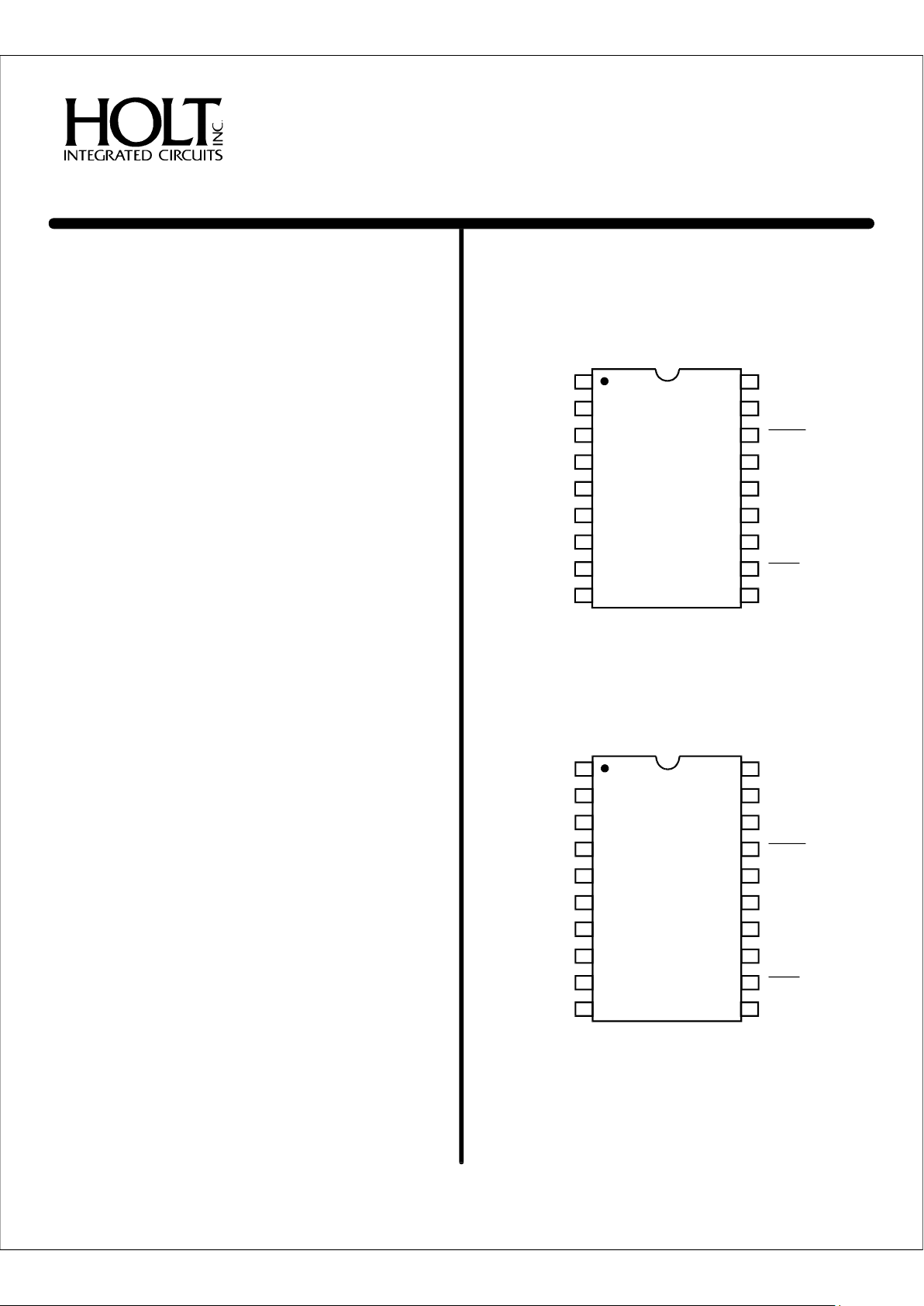
HI-8683
18-PinPlasticSOIC-WBPackage
HI-8684
20-PinPlasticSOIC-WBPackage
HI-8683PSI
HI-8683PST
Vcc
GAPCLK
INB
INA
ERROR
PARITYENB
GND
RESET
READ
GAPCLK
TESTA
TESTB
RINB(-10)
RINA(-10)
ERROR
PARITYENB
GND
RESET
READ
Vcc
DATARDY
D7
D6
D5
D4
D3
D2
D1
D0
HOLTINTEGRATEDCIRCUITS
1(DS8683Rev.D)01/01
HI-8683,HI-8684
PINDESCRIPTIONS
DATARDYOUTPUTReceiverdatareadyflag.Ahighlevelindicatesdataisavailableinthereceive
buffer.Flaggoeslowwhenthefirst8-bitbyteisread.
D1toD7OUTPUT8-bitparalleldatabus(tri-state)
GNDPOWER0V
INPUTReadstrobe.Alowleveltransfersreceivebufferdatatothedatabus
PARITYENBINPUTParityEnable-Ahighlevelactivatesoddparitycheckingwhichreplacesthe
32ndARINCbitwithanerrorbit.Otherwise,the32ndARINCbitisunchanged
ERROROUTPUTErrorFlag.Ahighlevelindicatesabitcounterror(numberofARINCbitswas
lessthanorgreaterthan32)and/oraparityerr orifparitydetectionwasenabled
(PARITYENBhigh)
INAINPUTPositivedigitalserialdatainput(HI-8683only)
INBINPUTNegativedigitalserialdatainput(HI-8683only)
RINA/RINA-10INPUTPositivedirectARINCserialdatainput
RINB/RINB-10INPUTNegativedirectARINCserialdatainput(HI-8684&HI-8684-10only)
INPUTInternallogicstatesareinitializedwithalowlevel
TESTAINPUTUsedinconjunctionwiththeTESTBinputtobypassthebuilt-inanalogline
receivercircuitry
TESTBINPUTU
GAPCLKINPUTGapClock.DeterminestheminimumtimerequiredbetweenARINCwordsfor
dete ction.Theminimumwordgaptimeisbetween16and17clockcyclesof
thissignal.
VccPOWER+5V±10%supply
SIGNALFUNCTIONDESCRIPTION
READ
RESET
(HI-8684&HI-8684-10only)
(HI-8684&HI-8684-10only)
sedinconjunctionwiththeTESTAinputtobypassthebuilt-inanalogline
receivercircuitry(HI-8684&HI-8684-10only)
HOLTINTEGRATEDCIRCUITS
2
FUNCTIONALDESCRIPTION
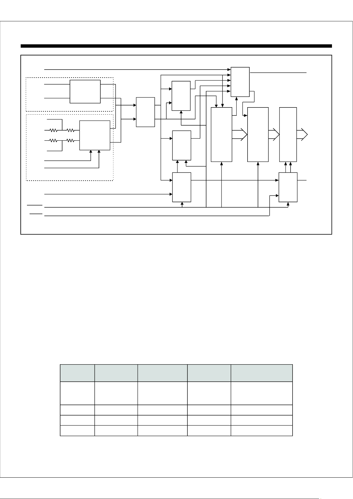
TheHI-8683andHI-8684areserialto8-bitparallelconverters.Theincomingdatastreamisseriallyshiftedintoaninput
register,checkedforerrors,andthentransferredinparallelto
a32-bitreceivebuffer.Thereceivedatacanbeaccessedusingfour8-bitparallelreadoperationswhilethenextserial
datasteamisbeingreceived.
Figure1isablockdiagramofboththeHI-8683andHI-8684.
ThedifferencebetweenthetwoproductsistheHI-8684has
abuilt-inlinereceiverwhereastheHI-8683isstrictlyadigital
deviceandrequiresanexternalARINClinereceiversuchas
theHolt HI-8482,HI-8588orHI-8590tointerfacetothe
ARINC429bus.
RECEIVERINPUTS
HI-8684LineReceiver
Typically35KresistorsareinserieswithboththeRINAand
RINBARINC429inputs.Theyconnecttoleveltranslators
whoseresistancetoGNDistypically10KAfterleveltranslation,thebufferedinputsdriveadifferentialamplifier.The
differentialsignaliscomparedtolevelsderivedfromadivider
betweenVCCandGND.Thenominalsettingscorrespondto
aOne/Zeroamplitudeof6.0VandaNullamplitudeof3.3V.A
validARINCOne/ZeroinputsetsalatchandaNullinputresetsthelatch.
Sinceanyaddedexternalseriesresistancewillaffectthevoltagetranslation,theHI-8684-10i savailablewith25Kofthe
35KseriesresistancerequiredforproperARINC429level
detection.Theremaining10Krequiredthatmustbeadded
canbeincorporatedinotherexternalcircuitrysuchaslightningprotection.Exceptforthedifferentinputseriesresistance,theHI-8684andHI-8684-10areidentical.
Ω
Ω.
Ω
Ω
Ω
HI-8683,HI-8684
HOLTINTEGRATEDCIRCUITS
3
PROTOCOLDETECTION
ARINCclockanddataintheHI-8683arederivedfromthe
twostreamsofdigitaldataattheINAandINBinputsandthe
resultingOne/Zerodataisshiftedintoa32-bitinputregister
asillustratedinFigure3.
IntheHI-8684,theOne/Zerodatashiftedintotheinputregisteriscreatedfromeitherthetwodigitaloutputsofthebuiltinlinereceiver(Figure3)ortheTESTAandTESTBinputs
(Figure4).
ForARINC561operation,theINAandINBdatastreamsinputsmustbederivedfromtheARINC561data,clockand
syncwithexternallogic.
GAPDETECTION
Theendofadatawordisdetectedbyaninternalcounter
thattimesoutwhenadataOneorZeroisnotreceivedfora
periodequalto16cyclesoftheGAPCLKsignal.Thegap
detectiontimemayvarybetween16and17cyclesofthe
GAPCLKsignalsincetheincomingdataandGAPCLKare
notusuallysynchronousinputs.Therequiredfrequencyof
GAPCLKisafunctionofthemininumgaptimespecifiedfor
thetypeofARINCdatabeingreceived.Table1indicates
typicalfrequenciesthatmaybeusedforthevariousdata
ratesnormallyencountered.
BIT
COUNT
PARITY
DETECT
GAP
DETECT
32-BIT
SHIFT
REG.
32-BIT
RECEIVE
BUFFER
32-BIT
TO
8-BIT
MUX
ERROR
DETECT
CLOCK
&
DATA
DETECT
HI-8683ONLY
HI-8684ONLY
INA
PARITY
ENB
INB
RINB
TESTA
TESTB
GAPCLK
RESET
BYTE
COUNT
READ
DATARDY
ERROR
32 8
32
Figure1.BlockDiagram
ESD
PROTECTION
&
LINE
RECEIVER
ESD
PROTECTION
DATABUSBITPERIODMINIMUMGAPGAPCLOCKGAPDETECTION
TYPE(s)(s)MHzTIME(s)µµµ
42910450.7521.3-22.7
1.016-17
1.510.7-11.3
42969-133310-5990.1160-170
57569-133310-5990.1160-170
56169-133103-2000.280-85
Table1-TypicalGapDetectionTimes
FUNCTIONALDESCRIPTION(cont.)
RXA
RXB
10K Ω
BIT32
BIT32
RINA
D0-D7
DATA
CLK
RINB-10
RINA-10
10K Ω
25K Ω
25K Ω
 Loading...