

Datasheet HI-8683PST, HI-8683PSI-10, HI-8683PSI, HI-8683PJT, HI-8683PJI-10 Datasheet (HOLT)
...
HI-8683,HI-8684
ARINCINTERFACEDEVICE
ARINC429&561SerialDatato8-BitParallelData
DESCRIPTION
TheHI-8683andHI-8684aresystemcomponentsfor
interfacingincomingARINC429signalsto8-bitparallel
datausingproven+5Vanalog/digitalCMOStechnology.
TheHI-8683isadigitaldevicethatrequiresanexternal
analoglinereceiversuchastheHI-8482orHI-8588
betweentheARINCbusandthedeviceinputs.TheHI-8684
incorporatesthedigitallogicandanaloglinereceiver
circuitryinasingledevice.
TheHI-8683isalsoavailableasasecondsourcetothe
DLS-11218pinDIPand28pinPLCC
packagepinouts.
ThereceiversontheHI-8684connectdirectlytotheARINC
429Busandtransl atetheincomingsignalstonormalCMOS
levels.Internalcomparatorlevelsaresetjustbelowthe
standard6.5voltminimumdatathresholdandjustabovethe
standard2.5voltmaximumnullthreshold.The-10version
oftheHI-8684allowstheincorporationofanexternal10K
resistanceinserieswitheachARINCinputforlightning
protectionwithoutaffectingARINCleveldetection.
Bothproductsofferhighspeed8-bitparallelbusinterface,a
32-bitbuffer,anderrordetectionforwordlengthandparity.
Aresetpinisalsoprovidedforpower-oninitialization.
withtheoriginal
Ω
!
!
AutomaticconversionofserialARINC429,575&
561datato8-bitparalleldata
Highspeedparallel8-bitdatabus
Errordetection-and
On-chiplinereceiveroption(HI-8684)
Inputhysteresisofatleast2volts(HI-8684)
Testinputsbypassanaloginputs(HI-8684)
Simplifiedlightningprotectionwiththeabilitytoadd
10Kohmexternalseriesresistors(HI-8684-10)
Plasticpackageoptions-surfacemount(SOIC),
PLCCandDIP
Militaryprocessingavailable
!
!
!
!
!
!
!
!
wordlengthparity
Resetinputforpower-oninitialization
FEATURES
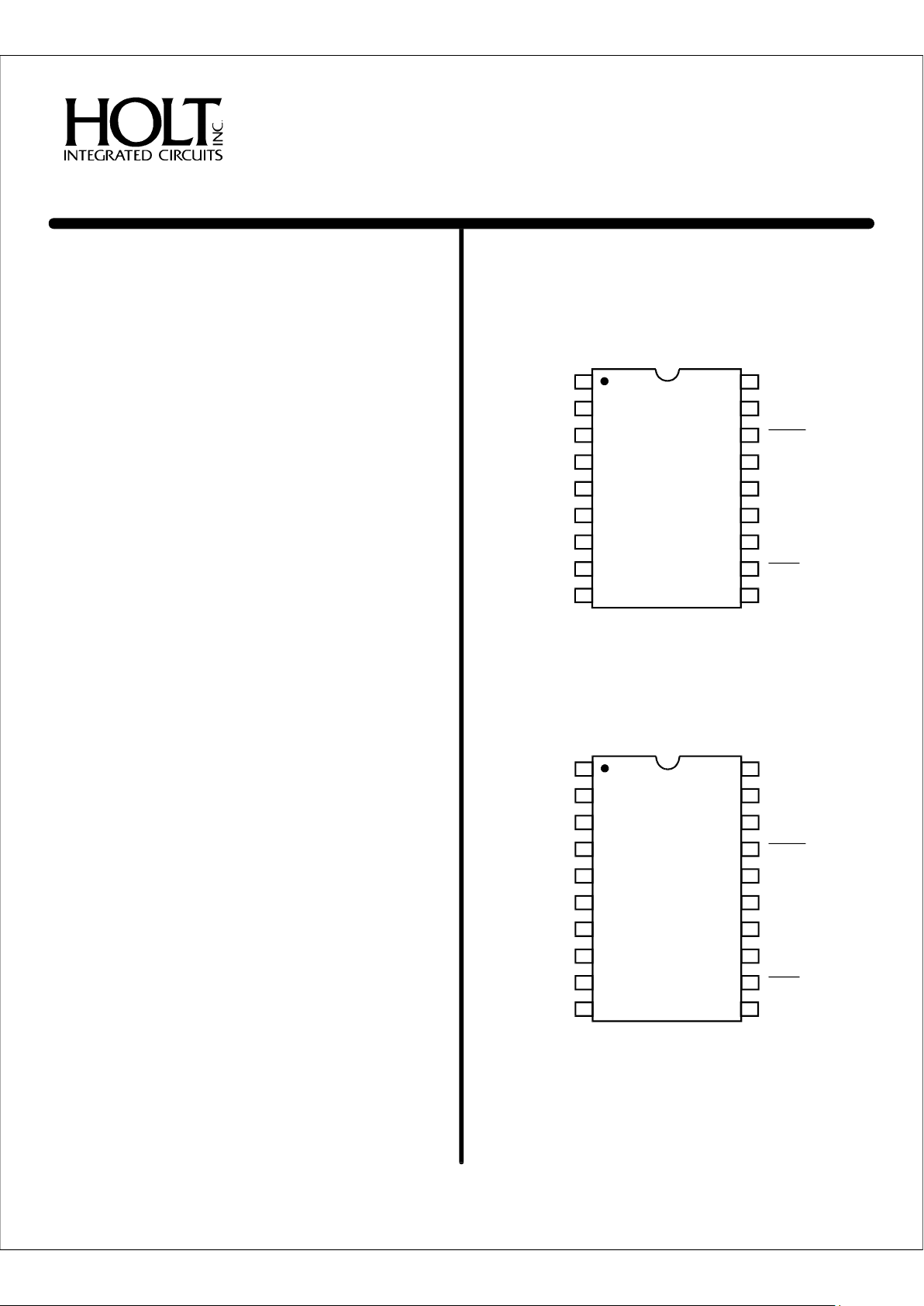
PINCONFIGURATIONS (TopView)
January2001
DATARDY
D7
D6
D5
D4
D3
D2
D1
D0
HI-8684PSI
HI-8684PST
&
HI-8684PSI-10
HI-8684PST-10
1
2
3
4
5
6
7
8
9
10
(Seepage8foradditionalpinconfigurations)
1
2
3
4
5
6
7
8
9
1
2
3
4
5
6
7
8
9
18
17
16
15
14
13
12
11
10
20
19
18
17
16
15
14
13
12
11
HI-8683
18-PinPlasticSOIC-WBPackage
HI-8684
20-PinPlasticSOIC-WBPackage
HI-8683PSI
HI-8683PST
Vcc
GAPCLK
INB
INA
ERROR
PARITYENB
GND
RESET
READ
GAPCLK
TESTA
TESTB
RINB(-10)
RINA(-10)
ERROR
PARITYENB
GND
RESET
READ
Vcc
DATARDY
D7
D6
D5
D4
D3
D2
D1
D0
HOLTINTEGRATEDCIRCUITS
1(DS8683Rev.D)01/01
HI-8683,HI-8684
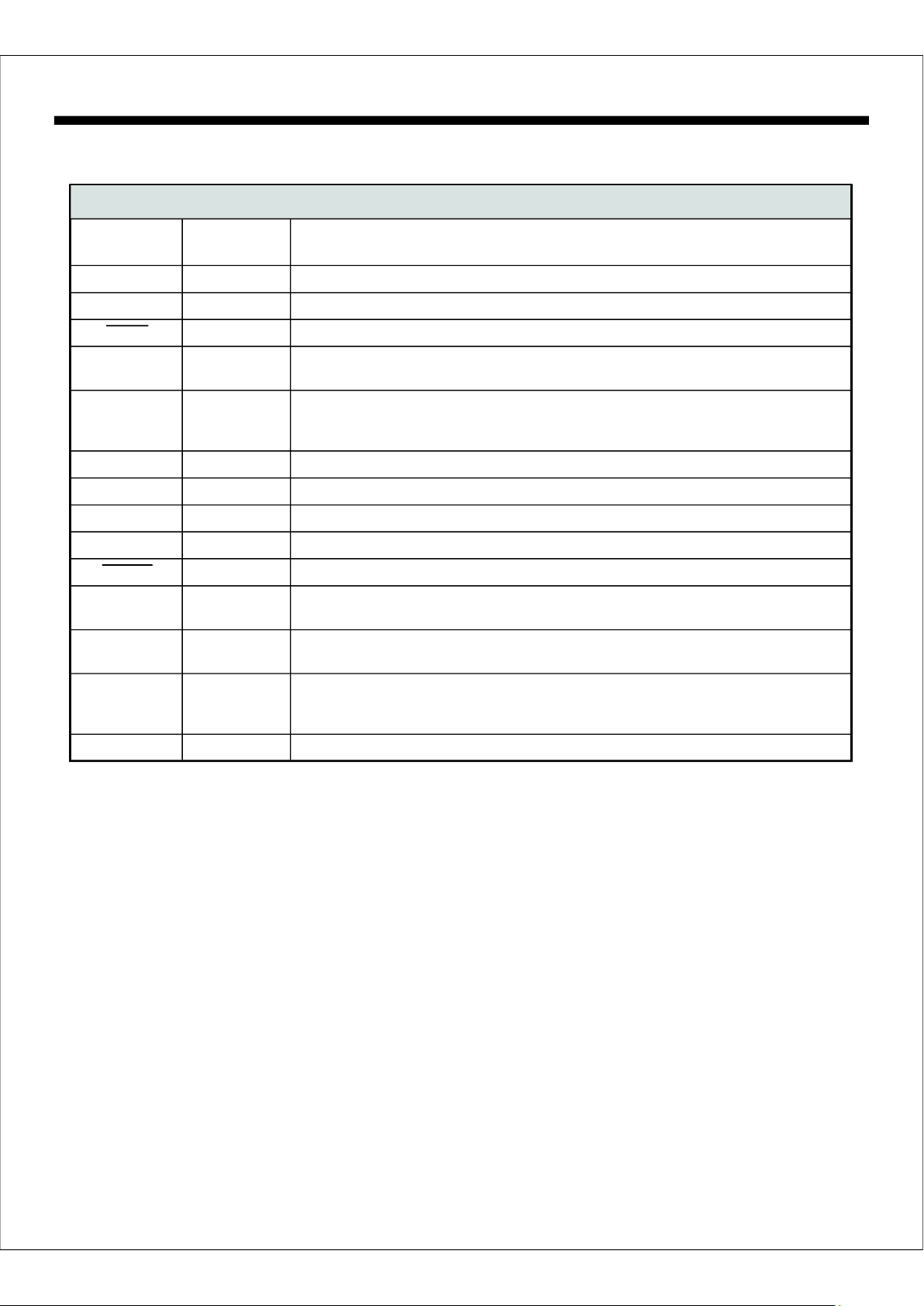
PINDESCRIPTIONS
DATARDYOUTPUTReceiverdatareadyflag.Ahighlevelindicatesdataisavailableinthereceive
buffer.Flaggoeslowwhenthefirst8-bitbyteisread.
D1toD7OUTPUT8-bitparalleldatabus(tri-state)
GNDPOWER0V
INPUTReadstrobe.Alowleveltransfersreceivebufferdatatothedatabus
PARITYENBINPUTParityEnable-Ahighlevelactivatesoddparitycheckingwhichreplacesthe
32ndARINCbitwithanerrorbit.Otherwise,the32ndARINCbitisunchanged
ERROROUTPUTErrorFlag.Ahighlevelindicatesabitcounterror(numberofARINCbitswas
lessthanorgreaterthan32)and/oraparityerr orifparitydetectionwasenabled
(PARITYENBhigh)
INAINPUTPositivedigitalserialdatainput(HI-8683only)
INBINPUTNegativedigitalserialdatainput(HI-8683only)
RINA/RINA-10INPUTPositivedirectARINCserialdatainput
RINB/RINB-10INPUTNegativedirectARINCserialdatainput(HI-8684&HI-8684-10only)
INPUTInternallogicstatesareinitializedwithalowlevel
TESTAINPUTUsedinconjunctionwiththeTESTBinputtobypassthebuilt-inanalogline
receivercircuitry
TESTBINPUTU
GAPCLKINPUTGapClock.DeterminestheminimumtimerequiredbetweenARINCwordsfor
dete ction.Theminimumwordgaptimeisbetween16and17clockcyclesof
thissignal.
VccPOWER+5V±10%supply
SIGNALFUNCTIONDESCRIPTION
READ
RESET
(HI-8684&HI-8684-10only)
(HI-8684&HI-8684-10only)
sedinconjunctionwiththeTESTAinputtobypassthebuilt-inanalogline
receivercircuitry(HI-8684&HI-8684-10only)
HOLTINTEGRATEDCIRCUITS
2
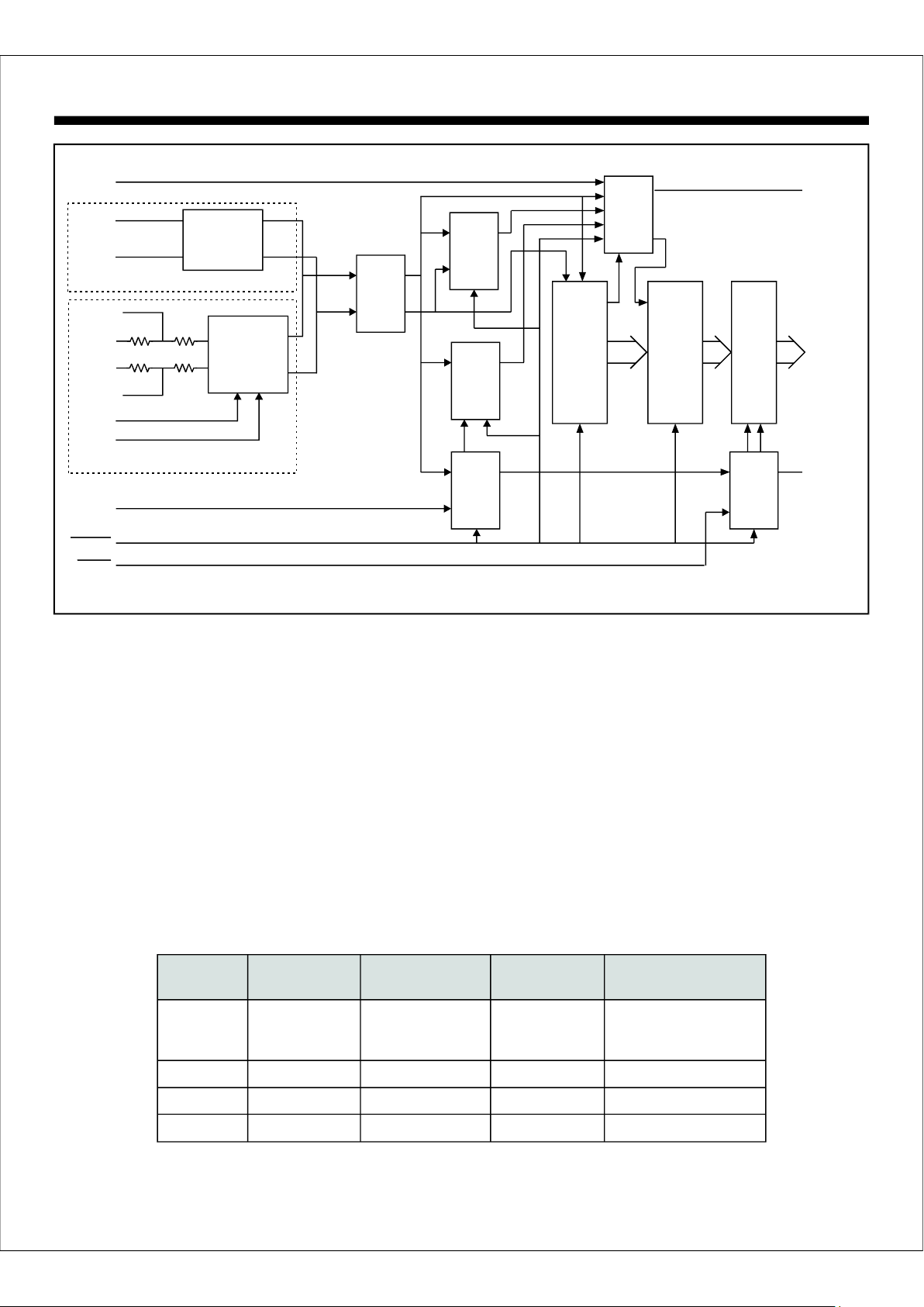
FUNCTIONALDESCRIPTION
TheHI-8683andHI-8684areserialto8-bitparallelconverters.Theincomingdatastreamisseriallyshiftedintoaninput
register,checkedforerrors,andthentransferredinparallelto
a32-bitreceivebuffer.Thereceivedatacanbeaccessedusingfour8-bitparallelreadoperationswhilethenextserial
datasteamisbeingreceived.
Figure1isablockdiagramofboththeHI-8683andHI-8684.
ThedifferencebetweenthetwoproductsistheHI-8684has
abuilt-inlinereceiverwhereastheHI-8683isstrictlyadigital
deviceandrequiresanexternalARINClinereceiversuchas
theHolt HI-8482,HI-8588orHI-8590tointerfacetothe
ARINC429bus.
RECEIVERINPUTS
HI-8684LineReceiver
Typically35KresistorsareinserieswithboththeRINAand
RINBARINC429inputs.Theyconnecttoleveltranslators
whoseresistancetoGNDistypically10KAfterleveltranslation,thebufferedinputsdriveadifferentialamplifier.The
differentialsignaliscomparedtolevelsderivedfromadivider
betweenVCCandGND.Thenominalsettingscorrespondto
aOne/Zeroamplitudeof6.0VandaNullamplitudeof3.3V.A
validARINCOne/ZeroinputsetsalatchandaNullinputresetsthelatch.
Sinceanyaddedexternalseriesresistancewillaffectthevoltagetranslation,theHI-8684-10i savailablewith25Kofthe
35KseriesresistancerequiredforproperARINC429level
detection.Theremaining10Krequiredthatmustbeadded
canbeincorporatedinotherexternalcircuitrysuchaslightningprotection.Exceptforthedifferentinputseriesresistance,theHI-8684andHI-8684-10areidentical.
Ω
Ω.
Ω
Ω
Ω
HI-8683,HI-8684
HOLTINTEGRATEDCIRCUITS
3
PROTOCOLDETECTION
ARINCclockanddataintheHI-8683arederivedfromthe
twostreamsofdigitaldataattheINAandINBinputsandthe
resultingOne/Zerodataisshiftedintoa32-bitinputregister
asillustratedinFigure3.
IntheHI-8684,theOne/Zerodatashiftedintotheinputregisteriscreatedfromeitherthetwodigitaloutputsofthebuiltinlinereceiver(Figure3)ortheTESTAandTESTBinputs
(Figure4).
ForARINC561operation,theINAandINBdatastreamsinputsmustbederivedfromtheARINC561data,clockand
syncwithexternallogic.
GAPDETECTION
Theendofadatawordisdetectedbyaninternalcounter
thattimesoutwhenadataOneorZeroisnotreceivedfora
periodequalto16cyclesoftheGAPCLKsignal.Thegap
detectiontimemayvarybetween16and17cyclesofthe
GAPCLKsignalsincetheincomingdataandGAPCLKare
notusuallysynchronousinputs.Therequiredfrequencyof
GAPCLKisafunctionofthemininumgaptimespecifiedfor
thetypeofARINCdatabeingreceived.Table1indicates
typicalfrequenciesthatmaybeusedforthevariousdata
ratesnormallyencountered.
BIT
COUNT
PARITY
DETECT
GAP
DETECT
32-BIT
SHIFT
REG.
32-BIT
RECEIVE
BUFFER
32-BIT
TO
8-BIT
MUX
ERROR
DETECT
CLOCK
&
DATA
DETECT
HI-8683ONLY
HI-8684ONLY
INA
PARITY
ENB
INB
RINB
TESTA
TESTB
GAPCLK
RESET
BYTE
COUNT
READ
DATARDY
ERROR
32 8
32
Figure1.BlockDiagram
ESD
PROTECTION
&
LINE
RECEIVER
ESD
PROTECTION
DATABUSBITPERIODMINIMUMGAPGAPCLOCKGAPDETECTION
TYPE(s)(s)MHzTIME(s)µµµ
42910450.7521.3-22.7
1.016-17
1.510.7-11.3
42969-133310-5990.1160-170
57569-133310-5990.1160-170
56169-133103-2000.280-85
Table1-TypicalGapDetectionTimes
FUNCTIONALDESCRIPTION(cont.)
RXA
RXB
10K Ω
BIT32
BIT32
RINA
D0-D7
DATA
CLK
RINB-10
RINA-10
10K Ω
25K Ω
25K Ω

HI-8683,HI-8684
HOLTINTEGRATEDCIRCUITS
4
ERRORCHECKING
READINGRECEIVEBUFFER
Onceawordgapisdetected,thedatawordintheinputregisteristransferredtothereceivebufferandcheckedforerrors.
Whenparitydetectionisenabled(PARITYENBhigh),the
receivedwordischeckedforoddparity.Ifthereisaparity
error,the32ndbitofthereceiveddatawordissethigh.
Ifparitycheckingisdisabled(PARITYENBlow)the32nd
bitofthedatawordisalwaysthe32ndARINCbitreceived.
TheERRORflagoutputissethighuponreceiptofaword
gapandthenumberofbitsreceivedsincetheprevious
wordgapislessthanorgreaterthan32.TheERRORflag
isresetlowwhenthenext validARINCwordiswritteninto
thereceivebufferorwhenispulsedlow.
Whenthedatawordistransferredtothereceivebuffer,the
DATARDYpingoeshigh.Thedatawordcanthenberead
infour8-bitbytesbypulsingtheinputlowasindicatedinFigure5.ThefirstreadcycleresetsDATARDY
lowandincrementsaninternalcountertothenext8-bit
byte.Thecountercontinuestoincrementoneachreadcycleuntilallfourbytesareread.Therelationshipbetween
eachbitofanARINCwordreceivedandeachbitofthefour
8-bitdatabusbytesisspecifiedinFigure2.
WhenanewARINCwordisreceivedi talwaysoverwrites
thereceivebuffer.Ifthefirstbyteofthepreviouswordhas
notbeenread,thenpreviousdataislostandthereceive
bufferwillcontainthenewARINCword.However,ifthe
DATARDYpingoeshighbetweenthereadingofthefirst
andfourthbytes,thepreviousreadbytesarenolonger
validbecausetheunreadbyteshavebeenoverwrittenby
thenewARINCword.Also,thenextreadwillbeofthefirst
byteofthenewARINCwordsincetheinternalbytecounter
isalwaysresettothefirstbytewhennewdataistransferredtothereceivebuffer.
RESET
READ
FUNCTIONALDESCRIPTION(cont.)
TRUTHTABLE1.
RINARINBTESTATESTBRXARXB
-1.50to+1.50V-1.50Vto+1.50V0000
-3.25Vto-6.50V+3.25Vto+6.50V0001
+3.25Vto+6.50V-3.25Vto-6.50V0010
XX0101
XX1010
XX1100
X=don'tcare
ReadByteDataBusBitsARINCBits
1stByte1D0-D7ARINC1-ARINC8
2ndByte2D0-D7ARINC9-ARINC16
3rdByte3D0-D7ARINC17-ARINC24
4thByte4D0-D7ARINC25-ARINC32
FIGURE2.ORDEROFRECEIVEDDATA
RESET
TESTMODE(HI-8684only)
Alowontheinputsetsaflip-flopwhichinitializes
theinternallogic.Whengoeshigh,theinternal
logicremainsintheinitializedstateuntilthefirstwordgapis
detectedpreventingreceptionofapartialword.
Thebuilt-indifferentiallinereceiverontheHI-8684canbe
disabledallowingthedataandclockdetectioncircuitryto
bedrivendirectlywithdigitalsignals.ThelogicalORfunctionoftheTESTAandTESTBisdefinedinTruthTable1.
Thetwoinputscanbeusedfortestingthereceiverlogicand
forinputtingARINC429typedataderivedfromanother
source/protocol.SeeFig ure4fortypicaltestinputtiming.
Thedeviceshouldalwaysbeinitializedwithimmediatelyafterenteringthetestmodetoclearapartialword
thatmayhavebeenreceivedsincethelastwordgap.Otherwise,anERRORconditionmayoccurandthefirst32
bitsofdataonthetestinputsmaynotbeproperlyreceived.
Also,whenenteringthetestmode,bothTESTAand
TESTBshouldbesethighandheldinthatstateforat
leastonewordgapperiod(17gapclocks)after
goeshigh.
Whenexitingthetestmode,bothtestinputsshouldbeheld
lowandthedeviceinitializedwith
RESET
RESET
RESET
RESET
RESET.

HOLTINTEGRATEDCIRCUITS
5
HI-8683,HI-8684
ARINCDataBitsWordGap
2829303132124BitPeriodsMin.
INA(HI-8683only)
INB(HI-8683only)
VDIFF
RINA-RINB
(HI-8684only)
DERIVEDDATA
DERIVEDCLOCK
0V
0V
+5V
0V
+10V
+5V
-10V
TIMINGDIAGRAMS
FIGURE3-RECEIVERINPUTTIMINGFORARINC429
FIGURE5-RECEIVERPARALLELDATABUSTIMING
DATARDY
READ
D0-D7
VALID
t
RDYCLR
t
RDPW
t
RR
t
FD
t
RD
VALID VALID VALID
1st8-bits 2nd8-bits 3rd8-bits 4th8-bits
t
DRDY
DERIVEDDATA
32nd
ARINCBit
FIGURE4-TESTINPUTTIMINGFORARINC429
ARINCDataBitsWordGap
2829303132124BitPeriodsMin.
TESTA
+5V
0V
TESTB
0V
+5V
DERIVEDCLOCK
DERIVEDDATA

PARAMETERSSYMBOLTESTCONDITIONSMINTYPMAXUNITS
ARINCBusInputs (RINA&RINB,HI-8684only)
Differentialinputvoltage
oneorzeroVdifferentialvoltage6.510.013.0volts
nullV""""--2.75volts
commonmodeVwithrespecttoGND--5.0volts
Inputresistance
RINA(-10)toRINB(-10)Rsuppliesfloating3075-Kohm
RINA(-10)orRINB(-10)toGNDorVR"""'1940-Kohm
Inputcapacitance(Guaranteedbutnottested)
differentialCRINAtoRINB--20pF
toGNDC--20pF
toVC--20pF
DIN
NIN
COM
DIFF
CCSUP
DIFF
G
CCH
SupplyVoltages
V.................................................+5V
TemperatureRange
IndustrialScreening..............-40°Cto+85°C
Hi-TempScreening..............-55°Cto+125°C
MilitaryScreening..................-55°Cto+125°C
JunctionTemperature,Tj....................175°C
CC ±10%
≤+
AllvoltagesreferencedtoGND
Supplyvoltages
V.......................................................+7.0V
Voltageoninputs
RINA(-10)toRINB(-10).........+29Vto-29V
Allotherinputpins..................-0.3toVcc+0.3
DCcurrentperinputpin.......................+10mA
Powerdissipationat25°C
plastic18-pinSO.....1.9W,derate15.4mW/°C
plastic18-pinDIP.....1.6
plastic20-pinSO......1.4
plastic20-pinPLCC.2.0
SolderTemperature
Leads................................+280°Cfor10sec
Packagebody.....................................+2 20°C
StorageTemperature.............-65°Cto+150°C
CC
W,derate13.3mW/°C
W,derate11.5mW/°C
W,derate17.2mW/°C
NOTE:Stressesaboveabsolutemaximum
ratingsoroutsiderecommendedoperating
conditionsmaycausepermanentdamageto
thedevice.Thesearestressratingsonly.
Operationatthelimitsisnotrecommended.
ABSOLUTEMAXIMUMRATINGS
RECOMMENDEDOPERATINGCONDITIONS
Vcc=5V,GND=0V,TA=OperatingTemperatureRange(unlessotherwisespecified).
DCELECTRICALCHARACTERISTICS
HI-8683,HI-8684
HOLTINTEGRATEDCIRCUITS
6

Vcc=5V,GND=0V,TA=OperatingTemperatureRange(unlessotherwisespecified).
HI-8683,HI-8684
HOLTINTEGRATEDCIRCUITS
7
DCELECTRICALCHARACTERISTICS(cont.)
PARAMETERSSYMBOLTESTCONDITIONSMINTYPMAXUNITS
DigitalInputs
Outputs
OperatingSupplyCurrent
(INA,INB,,GAPCLK,,PARITYENA,TESTA&TESTB)
Inputvoltage
highV2.0-V
lowV0.0-0.8volts
Inputcurrent
source--1.0
sink-1.0--
InputcapacitanceC--8.0pF
(D0toD7,ERROR&DATARDY)
Outputvoltage
high
lowI=1.6mA--0.4volts
Outputtri-statecurrent(D0-D7only)
V=5.0V--1.0A
V=0.0V-1.0--
Outputcapacitance--15pF
V(HI-8683only)IV=0.0V,outputsopen--0.2m
V(HI-8684only)IV=0.0V,outputsopen--6.5m
RESETREAD
IHCC
IL
I
OL
OH
OL
CCCC1IN
CCCC2IN
µ
volts
IV=5.0VA
IV=0.0VA
VI=-1.0mA2.7--volts
V
I
IA
C
A
A
IHIN
ILIN
OHOH
OL
IH
IL
O
µ
µ
µ
PARAMETERSSYMBOLTESTCONDITIONSMINTYPMAXUNITS
pulsewidtht50ns
Datadelayfromt20ns
todatafloatingt20ns
toDATARDYcleart25ns
pulsetonextpulset25ns
GAPCLKfrequencyf1MHz
32ARINCbittoDATARDYt1617clocks
READ
READ
READ
READ
READREAD
RDPW
RD
FD
RDYCLR
RR
GC
DRDY
ACELECTRICALCHARACTERISTICS
Vcc=5V,GND=0V,TA=OperatingTemperatureRange(unlessotherwisespecified).

HI-8683&HI-8684PINCONFIGURATIONS
(Seepage1foradditionalpinconfigurations)
HI-8683,HI-8684
HOLTINTEGRATEDCIRCUITS
8
HI-8683PJI
HI-8683PJT
18-N/A
1716-INB
15-INA
14-ERROR
RESET
D6-4
D5-5
D4-6
D3-7
D2-8
V
GAPCLK
INB
INA
ERROR
PARITY
ENB
D0
CC
RESET
READ
DATA
RDY
D6
D7
D5
D4
D3
D2
D1
GND
1
2
3
4
5
6
7
8
9
18
17
16
15
14
13
12
11
10
HI-8683PDI
HI-8683PDT
HI-8684PJI
HI-8684PJT
&
HI-8684PJI-10
HI-8684PJT-10
18-TESTB
1716-RINB(-10)
15-RINA(-10)
14-ERROR
RESET
D6-4
D5-5
D4-6
D3-7
D2-8
HI-8683
20-PinPlasticPLCC
HI-8684
20-PinPlasticPLCC
HI-8683
18-PinPlasticDIP
ORDERINGINFORMATION
HI-8683PDI18PINPLASTICDIPNONO-40°CTO+85°CINOSOLDER
HI-8683PDT18PINPLASTICDIPNO-55°CTO+125°CTNOSOLDER
HI-8683PJI20PINPLASTICPLCCNO
BUILT-IN
PARTPACKAGELINE10KRES.TEMPERATUREBURNLEAD
NUMBERDESCRIPTIONRECV'RREQUIREDRANGEFLOWINFINISH
Ω
NO
NO-40°CTO+85°CINOSOLDER
HI-8683PJT20PINPLASTICPLCCNONO-55°CTO+125°CTNOSOLDER
HI-8683PSI18PINPLASTICSOIC-WBNONO-40°CTO+85°CINOSOLDER
HI-8683PST18PINPLASTICSOIC-WBNONO-55°CTO+125°CTNOSOLDER
HI-8684PJI20PINPLASTICPLCCYESNO-40°CTO+85°CINOSOLDER
HI-8684PJT20PINPLASTICPLCCYESNO-55°CTO+125°CTNOSOLDER
HI-8684PSI20PINPLASTICSOIC-WBYESNO-40°CTO+85°CINOSOLDER
HI-8684PST20PINPLASTICSOIC-WBYESNO-55°CTO+125°CTNOSOLDER
HI-8684PJI-1020PINPLASTICPLCCYESYES-40°CTO+85°CINOSOLDER
HI-8684PJT-1020PINPLASTICPLCCYESYES-55°CTO +125°CTNOSOLDER
HI-8684PSI-1020PINPLASTICSOIC-WBYESYES-40°CTO+85°CINOSOLDER
HI-8684PST-1020PINPLASTICSOIC-WBYESYES-55°CTO+125°CTNOSOLDER
Legend:WB-WideBody

°
.454±.008
(11.531±.203)
.4065±.0125
(10.325±.318)
.293±.006
(7.442±.152)
.050
(1.27)
0°to8°
.033±.017
(.838±.432)
.090±.010
(2.286±.254)
.0075±.0035
(.191±.089)
TYP
.018
(.457)
TYP
SEEDETAILA
DETAILA
PackageType:
18-PINPLASTICSMALLOUTLINE(SOIC)-WB
(WideBody)
18HW
.0105±.0015
(.2667±.0381)
.905 ± .015
(22.99 ± .381)
.300 ± .010
(7.62 ± .254)
.335±.035
(8.509 ± .889)
0 ° ~15
.135 ± .015
(3.429 ± .381)
.100 ± .010
(2.540 ± .254)
.055 ± .010
(1.397 ± .254)
.019 ± .004
(.483 ± .102)
.130 ± .020
(3.302 ± .508)
.160 ± .025
(4.064 ± .635)
.250 ± .010
(6.350 ± .254)
7 ° TYP.
.0115±.0035
(.2921±.0889)
HI-8683,HI-8684PACKAGEDIMENSIONS
inches(millimeters)
HOLTINTEGRATEDCIRCUITS
9
PackageType:
18-PINPLASTICDIP
18P

.5035±.0075
(12.789±.191)
.4065±.0125
(10.325±.318)
.296±.003
(7.518±.076)
0°to8°
.090±.010
(2.286±.254)
.0075±.0035
(.191±.089)
.050
(1.27)
TYP
.018
(.457)
TYP
SEEDETAILA
DETAILA
.033±.017
(.838±.432)
PackageType:
20-PINPLASTICSMALLOUTLINE(SOIC)-WB
(WideBody)
20HW
.0105±.0015
(.2667±.0381)
.152±.002
(.3.861±.051)
PINNO.1IDENT
.045x45°
.354 ± .002
(8.991 ± .051)
.390 ± .005
(9.906 ± .127)
SQ.
SQ.
SEEDETAIL
A
.017 ± .004
(.432 ± .102)
DETAILA
.020MIN
(.508 ΜΙΝ
.015 ± .002
(.381 ± .051)
.050 ± .003
(1.27 ± .075 )
)
.026±.003x30°
(.660±.076x30°)
.035R
(.889R)
TYP
.010±.0003
(.256±.0076)
.020MIN
(.508MIN)
.320±.010
(8.128±.254)
inches(millimeters)
PackageType:
20-PINPLASTICPLCC
20J
HI-8683,HI-8684PACKAGEDIMENSIONS
HOLTINTEGRATEDCIRCUITS
10
 Loading...