

Page 1
June2001
HI-8581
GENERALDESCRIPTION
TheHI-8581devicefromHoltIntegratedCircuitsisasilicon
gateCMOSdeviceforinterfacinga16-bitparalleldatabus
directlytotheARINC429serialbus.Thedeviceprovides
tworeceivers,anindependenttransmitterandlinedriver
capabilityinasinglepackage.Thereceiverinputcircuitry
andlogicaredesignedtomeettheARINC429
specificationsforloading,leveldetection,timing,and
protocol.ThetransmittersectionprovidestheARINC429
communicationprotocolandthelinedrivercircuitsprovide
theARINC429outputlevels.
The16-bitparalleldatabusexchangesthe32-bitARINC
datawordintwostepswheneitherloadingthetransmitter
orinterrogatingthereceivers.Thedatabusinterfaceswith
CMOSandTTL.
Timingofallthecircuitrybeginswiththemasterclockinput,
CLK.ForARINC429applications,themasterclock
frequencyis1MHz.
Eachindependentreceivermonitorsthedatastreamwitha
samplingrate10timesthedatarate.Thesamplingrateis
softwareselectableateither1MHzor125KHz.Theresults
ofaparitycheckareavailableasthe32ndARINCbit.The
HI-8581examinesthenullanddatatimingsandwillreject
erroneouspatterns.Forexample,witha125KHzclock
selection,thedatafrequencymustbebetween10.4KHz
and15.6KHz.
FEATURES
!
ARINCspecification429compatible
!
Directreceiverandtransmitterinterfaceto
ARINCbusinasingledevice.
!
16-Bitparalleldatabus.
!
Timingcontrol10timesthedatarate
!
Selectabledataclocks
!
ReceivererrorrejectionperARINC
specification429
!
Automatictransmitterdatatiming
!
Selftestmode
!
Parityfunctions
!
Lowpower
!
Industrial&fullmilitarytemperatureranges
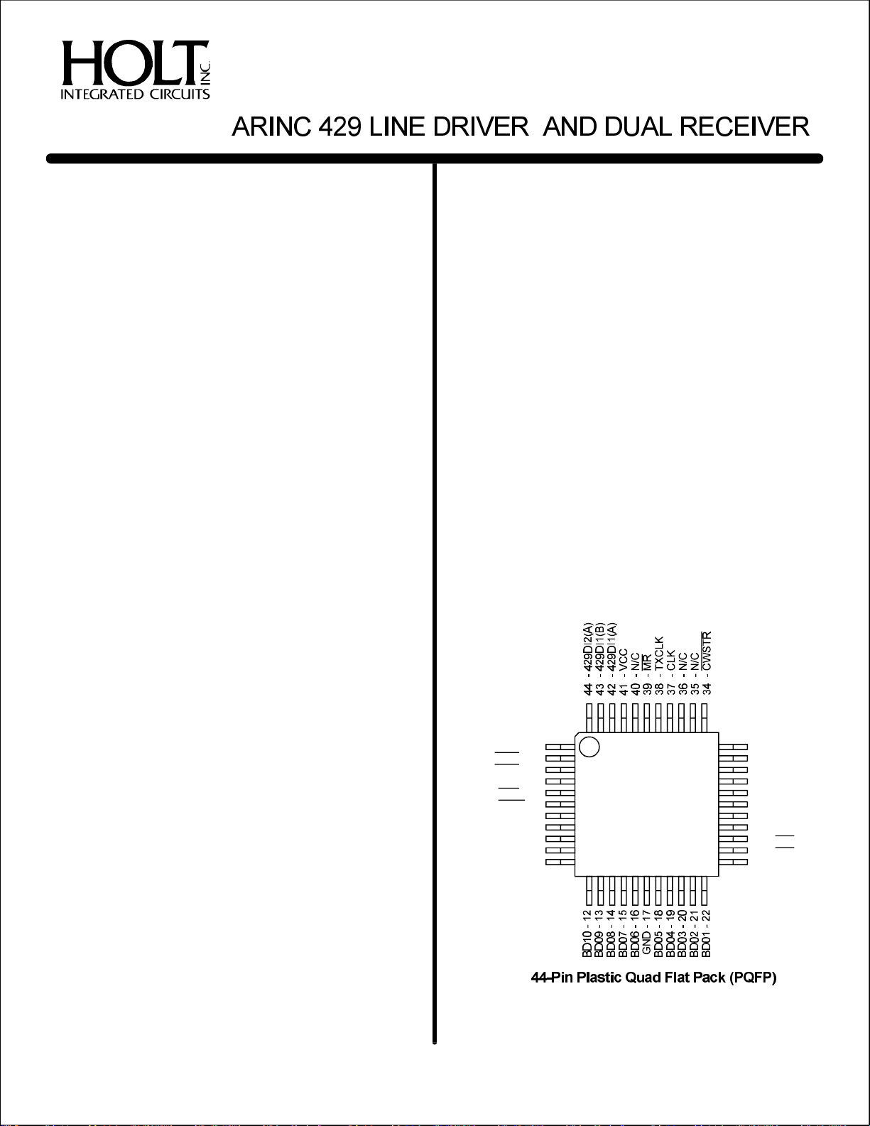
PINCONFIGURATION (TopView)
ThetransmitterhasaFirstIn,FirstOut(FIFO)memoryto
store8ARINCwordsfortransmission.Thedatarateofthe
transmitterissoftwareselectablebydividingthemaster
clock,CLK,byeither10or80.Themasterclockisusedto
setthetimingoftheARINCtransmissionwithintherequired
resolution.
APPLICATIONS
!
Avionicsdatacommunication
!
Serialtoparallelconversion
!
Paralleltoserialconversion
HOLTINTEGRATEDCIRCUITS
33-
429DI2(B)-1
1(DS8581Rev.A)06/01
-2
D/R1
-3
D/R2
SEL-4
-5
EN1
-6
EN2
BD15-7
BD14-8
BD13-9
BD12-10
BD11-11
(Seepage13foradditionalpinconfigurations)
HI-8581PQI
&
HI-8581PQT
ENTX
32-N/C
31-V+
30-TXB(OUT)
29-TXA(OUT)
28-V27-GND
26-TX/R
25-
PL2
24-
PL1
23-
BD00
Page 2
HI-8581
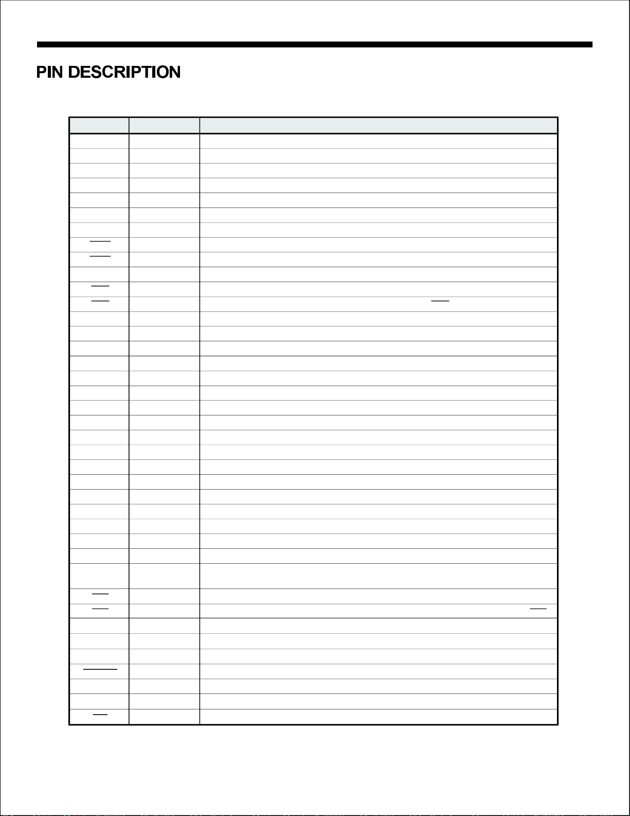
SIGNALFUNCTIONDESCRIPTION
VPOWER+5V±5%
CC
V+POWER+9.5Vto+12.6V
V-POWER-9.5Vto-12.6V
429DI1(A)INPUTARINCreceiver1positiveinput
429DI1(B)INPUTARINCreceiver1negativeinput
429DI2(A)INPUTARINCreceiver2positiveinput
429DI2(B)INPUTARINCreceiver2negativeinput
D/R1
D/R2
SELINPUTReceiverdatabyteselection(0=BYTE1)(1=BYTE2)
EN1
EN2EN1
BD15I/ODataBus
BD14I/ODataBus
BD13I/ODataBus
BD12I/ODataBus
BD11I/ODataBus
BD10I/ODataBus
BD09I/ODataBus
BD08I/ODataBus
BD07I/ODataBus
BD06I/ODataBus
GNDPOWER0V
BD05I/ODataBus
BD04I/ODataBus
BD03I/ODataBus
BD02I/ODataBus
BD01I/ODataBus
BD00I/ODataBus
TX/ROUTPUTTransmitterreadyflag.GoeslowwhenARINCwordloadedintoFIFO.Goeshigh
PL1
PL2PL1
TXA(OUT)OUTPUTLinedriveroutput-Aside
TXB(OUT)OUTPUTLinedriveroutput-Bside
ENTXINPUTEnableTransmission
CWSTR
CLKINPUTMasterClockinput
TXCLKOUTPUTTransmitterClockequaltoMasterClock(CLK),dividedbyeither10or80.
MR
OUTPUTReceiver1datareadyflag
OUTPUTReceiver2datareadyflag
INPUTDataBuscontrol,enablesreceiver1datatooutputs
INPUTDataBuscontrol,enablesreceiver2datatooutputsifishigh
AftertransmissionandFIFOempty.
INPUTLatchenableforbyte1enteredfromdatabustotransmitterFIFO.
INPUTLatchenableforbyte2enteredfromdatabustotransmitterFIFO.Mustfollow.
INPUTClockforcontrolwordregister
INPUTMasterReset,activelow
HOLTINTEGRATEDCIRCUITS
2
Page 3
HI-8581
FUNCTIONALDESCRIPTION
CONTROLWORDREGISTER
TheHI-8581contains10dataflipflopswhoseDinputsareconnectedtothedatabusandclocksconnectedto.Each
flipflopprovidesoptionstotheuserasfollows:
DATA
BUSFUNCTIONCONTROLDESCRIPTION
PIN
Ifenabled,aninternalconnection
BDO5SELFTEST0=ENABLEismadepassing429DOand
429DO
RECEIVER1Ifenabled,ARINCbits9and,
BDO6DECODER1=ENABLE10mustmatchthenexttwo
IfReceiver1Decoderis
BDO7--enabled,theARINCbit9
IfReceiver1Decoderis
BDO8--enabled,theARINCbit10
RECEIVER2Ifenabled,ARINCbits9and
BDO9DECODER1=ENABLE10mustmatchthenexttwo
IfReceiver2Decoderis
BD10--enabled,thenARINCbit9
IfReceiver2Decoderis
BD11--enabled,thenARINCbit10
INVERTLogic0enablesnormaloddparity
BD12XMTR1=ENABLEandLogic1enablesevenparity
PARITYoutputintransmitter32ndbit
BD13XMTRDATA0=÷10CLKisdividedeitherby10or
CLKSELECT1=÷8080toobtainXMTRdataclock
BD14RCVRDTA0=÷10CLKisdividedeitherby10or
CLKSELECT1=÷8080toobtainRCVRdataclock
CWSTR
tothereceiverlogicinputs
controlwordbits
mustmatchthisbit
mustmatchthisbit
controlwordbits
mustmatchthisbit
mustmatchthisbit
ARINC429DATAFORMAT
Thefollowingtableshowsthebitpositionsinexchangingdatawith
thereceiverorthetransmitter.ARINCbit1isthefirstbit
transmittedorreceived.
BYTE1
DATABDBDBDBDBDBDBDBDBDBDBDBDBDBDBDBD
BUS15141312111009080706050403020100
ARINC13121110931303212345678
BIT
BYTE2
DATABDBDBDBDBDBDBDBDBDBDBDBDBDBDBDBD
BUS15141312111009080706050403020100
ARINC29282726252423222120191817161514
BIT
THERECEIVERS
ARINCBUSINTERFACE
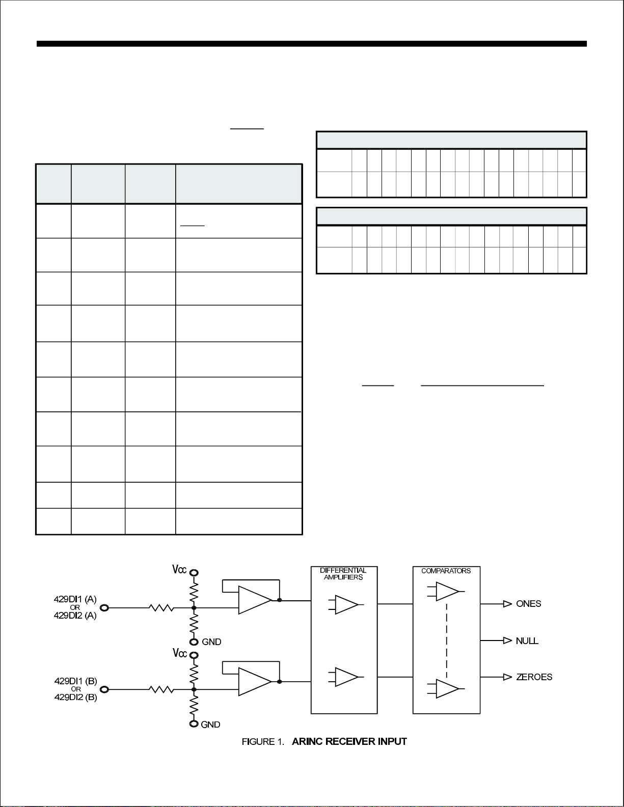
Figure1showstheinputcircuitforeachreceiver.TheARINC429
specificationrequiresthefollowingdetectionlevels:
STATEDIFFERENTIALVOLTAGE
ONE+6.5Voltsto+13Volts
NULL+2.5Voltsto-2.5Volts
ZERO-6.5Voltsto-13Volts
TheHI-8581guaranteesrecognitionoftheselevelswithacommon
modeVoltagewithrespecttoGNDlessthan±5Vfortheworstcase
condition(4.75Vsupplyand13Vsignallevel).
Thetolerancesinthedesignguaranteedetectionoftheabove
levels,sotheactualacceptancerangesareslightlylarger.Ifthe
ARINCsignalisoutoftheactualacceptanceranges,includingthe
nulls,thechiprejectsthedata.
HOLTINTEGRATEDCIRCUITS
3
Page 4
HI-8581
FUNCTIONALDESCRIPTION(con't)
RECEIVERLOGICOPERATION
Figure2showsablockdiagramofthelogicsectionofeachreceiver.
BITTIMING
TheARINC429specificationcontainsthefollowingtiming
specificationforthereceiveddata:
HIGHSPEEDLOWSPEED
BITRATE
PULSERISETIME
PULSEFALLTIME
PULSEWIDTH
AgaintheHI-8581acceptssignalsthatmeetthesespecifications
andrejectsoutsidethetolerances.Thewaythelogicoperation
achievesthisisdescribedbelow:
1.Keytotheperformanceofthetimingcheckinglogicisanaccurate1MHzclocksource.Lessthan0.1%errorisrecommended.
2.Thesamplingshiftregistersare10bitslongandmustshow
threeconsecutiveOnes,ZerosorNullstobeconsideredvalid
data.Additionally,fordatabits,theOneorZerointheupperbits
ofthesamplingshiftregistersmustbefollowedbyaNullinthe
lowerbitswithinthedatabittime.ForaNullinthewordgap,
threeconsecutiveNullsmustbefoundinboththeupperand
lowerbitsofthesamplingshiftregister.Inthismannertheminimumpulsewidthisguaranteed.
100KBPS±1%12K-14.5KBPS
1.5±0.5µsec10±5µsec
1.5±0.5µsec10±5µsec
5µsec±5%34.5to41.7µsec
TOPINS
3.Eachdatabitmustfollowitspredecessorbynotlessthan
8samplesandnomorethan12samples.Inthismannerthe
bitrateischecked.Withexactly1MHzinputclockfrequency,
theacceptabledatabitratesareasfollows:
HIGHSPEEDLOWSPEED
DATABITRATEMIN
DATABITRATEMAX
83KBPS10.4KBPS
125KBPS15.6KBPS
4.TheWordGaptimersamplestheNullshiftregisterevery
10inputclocks(80forlowspeed)afterthelastdatabitofa
Validreception.IftheNullispresent,theWordGapcounter
Isincremented.Acountof3willenablethenextreception.
RECEIVERPARITY
ThereceiverparitycircuitcountsOnesreceived,includingthe
paritybit,ARINCbit32.Iftheresultisodd,then"0"willappearin
the32ndbit.
RETRIEVINGDATA
Once32validbitsarerecognized,thereceiverlogicgeneratesan
EndofSequence(EOS).Ifthereceiverdecoderisenabledand
the9thand10thARINCbitsmatchthecontrolwordprogrambits
orifthereceiverdecoderisdisabled,thenEOSclocksthedata
readyflagflipfloptoa"1",or(orboth)willgolow.The
dataflagforareceiverwillremainlowuntilafterARINCbytes
D/R1D/R2
both
fromthatreceiverareretrieved.Thisisaccomplishedbyfirst
activatingwithSEL,thebyteselector,lowtoretrievethefirst
byteandthenactivatingwithSELhightoretrievethesecond
byte.retrievesdatafromreceiver1andretrievesdata
EN
EN
ENIEN2
fromreceiver2.
IfanotherARINCwordisreceived,andanewEOSoccursbefore
thetwobytesareretrieved,thedataisoverwrittenbythenew
word.
SEL
EN
D/R
DECODER
CONTROL
BITS
/
ONES
NULL
ZEROS
MUX
CONTROL
LATCH
ENABLE
CONTROL
EOS
BITS9&10
SHIFTREGISTER
SHIFTREGISTER
SHIFTREGISTER
32TO16DRIVER
32BITLATCH
32BITSHIFTREGISTER
BITCLOCK
WORDGAP
DATA
START
CONTROL
BITBD14
PARITY
CHECK
WORDGAP
SEQUENCE
CONTROL
DETECTION
TIMER
ERROR
FIGURE2. RECEIVERBLOCKDIAGRAM
HOLTINTEGRATEDCIRCUITS
4
32ND
BIT
CLOCK
OPTION
COUNTER
ENDOF
SEQUENCE
EOS
BITCLOCK
END
ERROR
CLOCK
CLK
CLOCK
BIT
AND
Page 5
HI-8581
TRANSMITTER
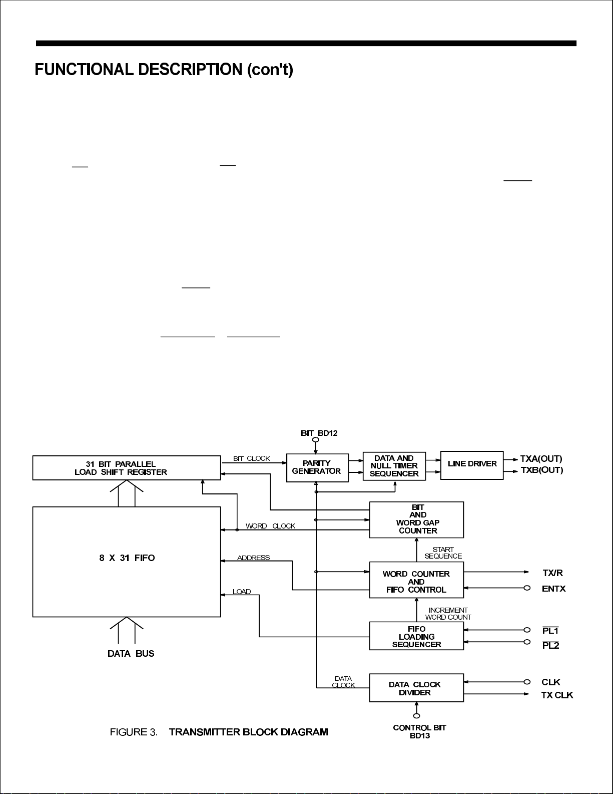
AblockdiagramofthetransmittersectionisshowninFigure3.
FIFOOPERATION
TheFIFOisloadedsequentiallybyfirstpulsingtoloadbyte1
andthentoloadbyte2.Thecontrollogicautomaticallyloads
the31bitwordinthenextavailablepositionoftheFIFO.IfTX/R,
thetransmitterreadyflagishigh(FIFOempty),then8words,
each31bitslong,maybeloaded.IfTX/Rislow,thenonlythe
availablepositionsmaybeloaded.Ifall8positionsarefull,the
FIFOignoresfurtherattemptstoloaddata.
PL2
DATATRANSMISSION
WhenENTXgoeshigh,enablingtransmission,theFIFO
positionsareincrementedwiththetopregisterloading intothe
datatransmissionshiftregister.Within2.5dataclocksthefirst
databitappearsateither429DOor.The31bitsinthe
datatransmissionshiftregisterarepresentedsequentiallytothe
outputsintheARINC429formatwiththefollowingtiming:
ARINCDATABITTIME10Clocks80Clocks
DATABITTIME5Clocks40Clocks
NULLBITTIME5Clocks40Clocks
WORDGAPTIME40Clocks320Clocks
429DO
HIGHSPEEDLOWSPEED
PL1
TRANSMITTERPARITY
TheparitygeneratorcountstheONESinthe31-bitword.Ifthe
BD12controlwordbitissetlow,the32ndbittransmittedwill
makeparityodd.Ifthecontrolbitishigh,theparityiseven.
SELFTEST
IftheBD05controlwordbitissetlow,429DOorbecome
inputstothereceiverbypassingtheinterfacecircuitry.
429DO
SYSTEMOPERATION
Thetworeceiversareindependentofthetransmitter.Therefore,
controlofdataexchangesisstrictlyattheoptionoftheuser.The
onlyrestrictionsare:
1.Thereceiveddatamaybeoverwrittenifnotretrieved
withinoneARINCwordcycle.
2.TheFIFOcanstore8wordsmaximumandignores
attemptstoloadadditiondataiffull.
3.Byte1ofthetransmitterdatamustbeloadedfirst.
4.Eitherbyteofthereceiveddatamayberetrievedfirst.
Bothbytesmustberetrievedtoclearthedatareadyflag.
Thewordcounterdetectswhenallloadedpositionsare
transmittedandsetsthetransmitterreadyflag,TX/R,high.
5.AfterENTX,transmissionenable,goeshighitcannotgo
lowuntilTX/R,transmitterreadyflag,goeshigh.Otherwise,
oneARINCwordislostduringtransmission.
HOLTINTEGRATEDCIRCUITS
5
Page 6

HI-8581
LINEDRIVEROPERATION
ThelinedriverintheHI-8581isdesignedtodirectlydrivetheARINC
429bus.ThetwoARINCoutputs(TXA(OUT)andTXB(OUT))
provideadifferentialvoltagetoproducea+10voltOne,a-10volt
Zero,anda0voltNull.SettingControlRegisterbit13tozero
causesaslopeof1.5sontheARINCoutputs;aoneinControl
Registerbit13causesaslopeof10s.Timingissetbyon-chip
resistorandcapacitorandtestedtobewithinARINCrequirements.
Noadditionalhardwareisrequiredtocontroltheslope.
has37.5ohmsinserieswitheachlinedriveroutput.
TXA(OUT)
TXB(OUT)
µ
ARINCBIT
DATA
BIT30
NULL
µ
TheHI-8581
DATA
NULL
BIT31
DATA
REPEATEROPERATION
Repeatermodeofoperationallowsadatawordthathasbeen
receivedbytheHI-8581tobeplaceddirectlyintoitsFIFOfor
transmission.Repeateroperationissimilartonormalreceiver
operation.Innormaloperation,eitherbyteofareceiveddata
wordmaybereadfromthereceiverlatchesfirstbyuseofSEL
input.Duringrepeateroperationhowever,thelowerbyteofthe
datawordmustbereadfirst.Thisisnecessarybecause,asthe
dataisbeingread,itisalsobeingloadedintotheFIFOandthe
transmitterFIFOisalwaysloadedwiththelowerbyteofthedata
wordfirst.Signalflowforrepeateroperationisshowninthe
TimingDiagramssection.
NULL
BIT32
WORDGAP
BIT1
NEXTWORD
DATABUS
CWSTR
DATABUS
VALID
t
CWSET
t
CWSTR
t
D/R
t
SELEN
t
D/REN
t
ENDATA
t
ENSEL
t
CWHLD
t
DATAEN
t
ENEN
t
ENDATA
t
SELEN
t
END/R
t
EN
t
ENSEL
t
DATAEN
HOLTINTEGRATEDCIRCUITS
6
Page 7

HI-8581
DATABUS
PL1
PL2
TX/R
PL2
TX/R
ENTX
TXA(OUT)
TXB(OUT)
t
PL2EN
t
ENDAT
t
t
PL
ARINCBIT
+5V
DWSET
BYTE1VALID
t
DWHLD
DATA
BIT1
t
PL12
ARINCBIT
DATA
BIT2
-5V
+5V
t
t
PL
BYTE2VALID
DWSET
t
DWHLD
t
TX/R
t
PL12
t
DTX/R
ARINCBIT
DATA
BIT32
+5V
t
ENTX/R
V
DIFF
(TXA(OUT)-TXB(OUT))
onelevel
10%
-5V
t
+10V
90%
t
rx
fx
zerolevel
10%
90%
t
fx
-10V
HOLTINTEGRATEDCIRCUITS
7
-5V
+10V
t
rx
nulllevel
Page 8

HI-8581
429DI
D/R
EN
SEL
PL1
PL2
TX/R
ENTX
TXA(OUT)
TXB(OUT)
BIT32
DON'TCARE
t
D/R
t
SELEN
t
D/REN
t
ENPL
t
END/R
t
EN
t
PLEN
t
ENEN
t
ENSEL
t
ENPL
t
EN
t
SELEN
t
TX/REN
t
PLEN
t
TX/R
t
ENSEL
t
DON'TCARE
ENDAT
BIT1 BIT32
t
t
DTX/R
ENTX/R
t
NULL
HOLTINTEGRATEDCIRCUITS
8
Page 9

InputResistance:DifferentialR12K
ToGNDR1227K
ToVccR1227K
InputVoltage:InputVoltageHIV2.1V
InputVoltage:InputVoltageHIV3.5V
HI-8581
SupplyVoltagesVcc-0.3Vto+7V
V++13.0V
V--13.0V
VoltageatpinsARINCinputs-29Vto+29V
Voltageatanyotherpin-0.3VtoVcc+0.3V
PowerDissipationat25C
PlasticPLCC/PQFP1.5W,derate10mW/C
CeramicJ-LEADCERQUAD1.0W,derate7mW/
DCCurrentDrainperpin±10mA
StorageTemperatureRange:-65°Cto+150°C
OperatingTemperatureRange:(Industrial)-40°Cto+85°C
(Military)-55°Cto+125°C
NOTE:Stressesabovethoselistedunder"AbsoluteMaximumRatings"maycausepermanentdamagetothedevice.Thesearestressratingsonly.
Functionaloperationofthedeviceattheseoranyotherconditionsabovethoseindicatedintheoperationalsectionsofthespecificationsisnotimplied.
Exposuretoabsolutemaximumratingconditionsforextendedperiodsmayaffectdevicereliability.
Vcc=5V±5%,GND=0V,TA=OperatingTemperatureRange(unlessotherwisespecified).V+=10V,V-=-10V,
LIMITS
PARAMETERCONDITIONSUNITSYMBOL
ARINCINPUTS
DifferentialInputVoltage:ONEVPins4to5,6to7:Common6.510.013.0V
ZEROVmodevoltagelessthan±4V-13.0-10.0-6.5V
NULLVwithrespecttoGND-2.502.5V
IH
IL
NUL
I
G
H
MINTYPMAX
°
°C
InputCurrent:InputSinkI200µA
InputSourceI-450µA
InputCapacitance:DifferentialCPins4to5,6to720pF
(Guaranteedbutnottested)ToGNDC20pF
ToVccC20pF
IH
IL
I
G
H
BI-DIRECTIONALINPUTS
InputVoltageLOV0.7V
InputCurrent:InputSinkI1.5µA
InputSourceI-1.5µA
IH
IL
IH
IL
OTHERINPUTS
InputVoltageLOV0.7V
InputCurrent:InputSinkI10µA
InputSourceI-20
IH
IL
IH
IL
HOLTINTEGRATEDCIRCUITS
9
Page 10

OutputVoltage:Logic"1"OutputVoltageVI=-1.5mA2.7V
HI-8581
Vcc=5V±5%,V+=10V,V-=-10V,GND=0V,TA=OperatingTemperatureRange(unlessotherwisespecified).
PARAMETERCONDITIONSUNITSYMBOL
ARINCOUTPUTS
ARINCoutputvoltage
OneorzeroVnoloadandmagnitudeatpin4.505.005.50V
NullV-0.250.25V
DOUT
NOUT""""""
LIMITS
MINTYPMAX
ARINCoutputcurrentI80mA
OUT
OTHEROUTPUTS
Logic"0"OutputVoltageVI=2.6mA0.4V
OutputCurrent:OutputSinkIV=0.4V3.0mA
(Bi-directionalPins)OutputSourceIV=V-0.4V1.1mA
OutputCurrent:OutputSinkIV=0.4V2.6mA
(AllOtherOutputs)OutputSourceIV=V-0.4V1.1mA
OutputCapacitance:C15pF
OHOH
OLOL
OLOUT
OHOUTCC
OLOUT
OHOUTCC
O
OperatingVoltageRange
V4.755.25V
CC
V+9.512.6V
V--9.5-12.6V
OperatingSupplyCurrent
VI20mA
CCCC1
V+I16mA
V-I16mA
DD1
EE1
HOLTINTEGRATEDCIRCUITS
10
Page 11

HI-8581
Vcc=5V,V+=10V,V-=-10V,GND=0V,TA=Oper.Temp.Rangeandfclk=1MHz0.1%with60/40dutycycle+
PARAMETERSYMBOLUNITS
LIMITS
MINTYPMAX
CONTROLWORDTIMING
PulseWidth-t50ns
Setup-DATABUSValidtoHIGHt50ns
Hold-HIGHtoDATABUSHi-Zt0ns
CWSTR
CWSTR
CWSTR
CWSTR
CWSET
CWHLD
RECEIVERTIMING
Delay-StartARINC32ndBittoLOW:HighSpeedt16µs
Delay-LOWtoHIGHt200ns
Delay-L0WtoDATABUSValidt5080ns
Delay-HIGHtoDATABUSHi-Zt30ns
Spacing-HIGHtonextL0Wt50ns
D/R
LowSpeedt128µs
Delay-LOWtoL0Wt0ns
D/REN
END/R
Setup-SELtoL0Wt0ns
Hold-SELtoHIGHt0ns
EN
EN
EN
EN
PulseWidth-ort8050ns
EN1EN2
ENEN
D/R
D/R
D/REN
END/R
SELEN
ENSEL
ENDATA
DATAEN
EN
ENEN
FIFOTIMING
PulseWidth-ort50ns
PL1PL2
PL
Setup-DATABUSValidtoHIGHt50ns
Hold-HIGHtoDATABUSHi-Zt0ns
PL
Spacing-ort0ns
Delay-HIGHtoTX/RLOWt840ns
PL2
PL
PL1PL2
DWSET
DWHLD
PL12
TX/R
TRANSMISSIONTIMING
Spacing-HIGHtoENTXHIGHt0µs
Delay-32ndARINCBittoTX/RHIGHt50ns
Spacing-TX/RHIGHtoENTX L0Wt0ns
PL2
PL2EN
DTX/R
ENTX/R
LINEDRIVEROUTPUTTIMING
Delay-ENTXHIGHtoTXA(OUT)orTXB(OUT):HighSpeedt25
Delay-ENTXHIGHtoTXA(OUT)orTXB(OUT):LowSpeedt200
ENDAT
ENDAT
Linedrivertransitiondifferentialtimes:
(HighSpeed)µs
(LowSpeed)hightolowt5.01015µs
hightolowt1.01.52.0
lowtohight1.01.52.0
lowtohight5.01015µs
fx
rx
fx
rx
µs
µs
µs
HOLTINTEGRATEDCIRCUITS
11
Page 12

HI-8581
Vcc=5V,V+=10V,V-=-10V,GND=0V,TA=Oper.Temp.Rangeandfclk=1MHz0.1%with60/40dutycycle+
LIMITS
PARAMETERSYMBOLUNITS
MINTYPMAX
REPEATEROPERATIONTIMING
Delay-LOWtoLOWt0nsENPL ENPL
Hold-HIGHtoHIGHt0ns
PLEN PLEN
Delay-TX/RLOWtoENTXHIGHt0ns
MasterResetPulseWidtht400ns
TX/REN
MR
ARINCDataRateandBitTiming±1%
HOLTINTEGRATEDCIRCUITS
12
Page 13

HI-8581
ADDITIONALHI-8581PINCONFIGURATION
(Seepage1foradditionalpinconfiguration)
ORDERINGINFORMATION
PART
NUMBER
HI-8581PJT
HI-8581CJT 44PINCERQUADJLEAD -55°CTO+125°C
HI-8581PQT
PACKAGE
DESCRIPTION
44PINPLASTICJLEAD
44PINPLASTICJLEAD
44PINCERQUADJLEAD
44PINPQFP
44PINPQFP
TEMPERATURE
RANGE
-40°CTO+85°CHI-8581PJI
-55°CTO+125°C
-40°CTO+85°CHI-8581CJI NO SOLDERI
-40°CTO+85°CHI-8581PQI NO SOLDERI
-55°CTO+125°C NO SOLDER
FLOW
I
T
T
T
BURN
IN
NO
NO
NO SOLDER
LEAD
FINISH
SOLDER
SOLDER
HOLTINTEGRATEDCIRCUITS
13
Page 14

44-PINPLASTICJ-LEADPLCC
HI-8581PACKAGEDIMENSIONS
inches(millimeters)
ACKAGEYPEPT:
PINNO.1
.045x45°
.690 ± .005
(17.526 ± .127)
SQ.
.172 ± .008
(4.369 ± .203)
.610 ± .020
(15.494± .508)
44-PINCERQUADJ-LEAD
PINNO.1IDENT
.653 ± .004
(16.586 ± .102)
SEEDETAIL
A
SQ.
.045x45°
DETAILA
.009
.011
.050 ± .005
(1.27 ± .127)
.031± .005
(.787 ± .127)
.017 ± .004
(.432 ± .102)
.015±.002
(.381 ±.051)
.020MIN
(.508 ΜΙΝ)
.025
R
.045
PackageType:
.039 ± .005
(.990 ± .127)
.650 ± .010
(16.510 ± .254)
.019 ± .002
(.483 ± .051)
214443
.688 ± .005
(17.475 ± .127)
MAX.
SQ.
SQ.
.200
MAX.
(5.080)
TYP.
.100 ± .007
(2.540 ± .178)
.050
(1.270)
HOLTINTEGRATEDCIRCUITS
14
.620 ± .012
(15.748 ± .305)
Page 15

HI-8581PACKAGEDIMENSIONS
44-PINPLASTICQUADFLATPACK(PQFP)
.097
(2.45)
.547±.010
(13.90±.25)
SQ.
SeeDetailA
MAX.
.394±.004
(10.0±.10)
SQ.
.079+.004/-.006
(2.00+.10/-.15)
.008
(.20R)
TYP.
PackageType:
.007
MAX.
(.17)
.0315BSC
(.80BSC)
.014±..002
(.35±.05)
.035+.006/-.004
(.88+.15/-.10)
.012
TYP.
(.30R)
DetailA
inches(millimeters)
44PQS
0°≤Θ≤7°
HOLTINTEGRATEDCIRCUITS
15
 Loading...