

HOLT HI-8282UT, HI-8282U, HI-8282ST, HI-8282SM-01, HI-8282S Datasheet
...
January2001
HI-8282
GENERALDESCRIPTION
TheHI-8282isasilicongateCMOSdeviceforinterfacing
theARINC429serialdatabustoa16-bitparalleldatabus.
Tworeceiversandanindependenttransmitterare
provided.Thereceiverinputcircuitryandlogicare
designedtomeettheARINC429specificationsforloading,
leveldetection,timing,andprotocol.Thetransmitter
sectionprovidestheARINC429communicationprotocol.
AdditionalinterfacecircuitrysuchastheHoltHI-8382is
requiredtotranslatethe5voltlogicoutputstoARINC429
drivelevels.
The16-bitparalleldatabusexchangesthe32-bitARINC
datawordintw ostepswheneitherloadingthetransmitter
orinterrogatingthereceivers.Thedatabusinterfaceswith
CMOSandTTL.
Timingofallthecircuitrybeginswiththemasterclockinput,
CLK.ForARINC429applications,themasterclock
frequencyis1MHz.
Eachindependentreceivermonitorsthedatastreamwitha
samplingrate10timesthedatarate.Thesamplingrateis
softwareselectableateither1MHzor125KHz.Theresults
ofaparitycheckareavailableasthe32ndARINCbit.The
HI-8282examinesthenullanddatatimingsandwillreject
erroneouspatterns.Forexample,witha125KHzclock
se lection,thedatafrequencymustbebetween10.4KHz
and15.6KHz.
FEATURES
!
ARINCspecification429compatible
!
16-Bitparalleldatabus
!
DirectreceiverinterfacetoARINCbus
!
Timingcontrol10timesthedatarate
!
Selectabledataclocks
!
ReceivererrorrejectionperARINC
specification429
!
Automatictransmitterdatatiming
!
Selftestmode
!
Parityfunctions
!
Lowpower,single5voltsupply
!
Industrial&fullmilitarytemperatureranges
! DESCSMDpartnumber
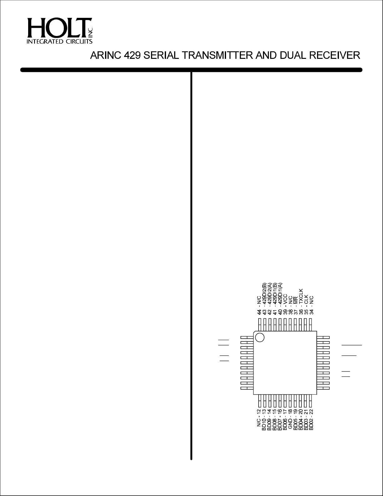
PINCONFIGURATION (TopView)
ThetransmitterhasaFirstIn,FirstOut(FIFO)memoryto
store8ARINCwordsfortransmission.Thedatarateofthe
transmitterissoftwareselectablebydividingthemaster
clock,CLK,byeither10or80.Themasterclockisusedto
setthetimingoftheARINCtransmissionwithintherequired
resolution.
APPLICATIONS
!
Avionicsdatacommunication
!
Serialtoparallelconversion
!
Paralleltoserialconversion
HOLTINTEGRATEDCIRCUITS
N/C-1
-2
D/R1
-3
D/R2
SEL-4
-5
EN1
-6
EN2
BD15-7
BD14-8
BD13-9
BD12-10
BD11-11
44-PinPlasticQuadFlatPack(PQFP)
(Seepage4-38foradditionalPackagePinConfigurations)
4-29(DS8282Rev.A) 01/01
HI-8282PQI
&
HI-8282PQT
33-N/C
32-N/C
31-
CWSTRX
30-ENTX
29-
429DO
28-429DO
27-TX/R
26-
PL2
25-
PL1
24-BD00
23-BD01

PINDESCRIPTION
SYMBOLFUNCTIONDESCRIPTION
VCCPOWER+5V±5%
429DI1(A)INPUTARINCreceiver1positiveinput
429DI1(B)INPUTARINCreceiver1negativeinput
429DI2(A)INPUTARINCreceiver2positiveinput
429DI2(B)INPUTARINCreceiver2negativeinput
D/R1
D/R2
SELINPUTReceiverdatabyteselection(0=BYTE1)(1=BYTE2)
EN1
EN2EN1
BD15I/ODataBus
BD14I/ODataBus
BD13I/ODataBus
BD12I/ODataBus
BD11I/ODataBus
BD10I/ODataBus
BD09I/ODataBus
BD08I/OData Bus
BD07I/ODataBus
BD06I/ODataBus
GNDPOWER0V
BD05I/ODataBus
BD04I/ODataBus
BD03I/ODataBus
BD02I/ODataBus
BD01I/ODataBus
BD00I/ODataBus
PL1
PL2PL1.
TX/ROUTPUTTransmitterreadyflag.GoeslowwhenARINCwordloadedintoFIFO.Goeshigh
429DOOUTPUT"ONES"dataoutputfromtransmitter.
429DO
ENTXINPUTEnableTransmission
CWSTR
CLKINPUTMasterClockinput
TXCLKOUTPUTTransmitterClockequaltoMasterClock(CLK),dividedbyeither10or80.
MR
OUTPUTReceiver1datareadyflag
OUTPUTReceiver2datareadyflag
INPUTDataBuscontrol,enablesreceiver1datatooutputs
INPUTDataBuscontrol,enablesreceiver2datatooutputsifishigh
INPUTLatchenableforbyte1enteredfromdatabustotransmitterFIFO.
INPUTLatchenableforbyte2enteredfromdatabustotransmitterFIFO.Mustfollow
OUTPUT"ZEROES"dataoutputfromtransmitter.
INPUTClockforcontrolwordregiste r
INPUTMasterReset,activelow
HI-8282
aftertransmissionandFIFOempty.
HOLTINTEGRATEDCIRCUITS
4-30
FUNCTIONALDESCRIPTION
CONTROLWORDREGISTER
TheHI-8282contains10dataflipflopswhoseDinputsareconnectedtothedatabusandclocksconnectedto.Each
flipflopprovidesoptionstotheuserasfollows:
DATA
BUSFUNCTIONCONTROLDESCRIPTION
PIN
CWSTR
ARINC429DATAFORMAT
Thefollowingtableshowsthebitpositionsinexchangingdatawith
thereceiverorthetransmitter.ARINCbit1isthefirstbit
transmittedorreceived.
BYTE1
DATABDBDBDBDBDBDBDBDBDBDBDBDBDBDBDBD
BUS15141312111009080706050403020100
ARINC13121110931303212345678
BIT
BDO5SELFTEST0=ENABLEismadepassing429DOand
RECEIVER1Ifenabled,ARINCbits9and,
BDO6DECODER1=ENABLE10mustmatchthenexttwo
BDO7--enabled,theARINCbit9
BDO8--enabled,theARINCbit10
RECEIVER2Ifenabled,ARINCbits9and
BDO9DECODER1=ENABLE10mustmatchthenexttwo
BD10--enabled,thenARINCbit9
BD11--enabled,thenARIN Cbit10
INVERTLogic0enablesnormaloddparity
BD12XMTR1=ENABLEandLogic1enablesevenparity
PARITYoutputintransmitter32ndbit
BD13XMTRDATA0=÷10CLKisdividedeitherby10or
CLKSELECT1=÷8080toobtainXMTRdataclock
BD14RCVRDTA0=÷10CLKisdividedeitherby10or
CLKSELECT1=÷8080toobtainRCVRdataclock
Ifenabled,aninternalconnection
tothereceiverlogicinputs
429DO
controlwordbits
IfReceiver1Decoderis
mustmatchthisbit
IfReceiver1Decoderis
mustmatchthisbit
controlwordbits
IfReceiver2Decoderis
mustmatchthisbit
IfReceiver2Decoderis
mustmatchthisbit
BYTE2
DATABDBDBDBDBDBDBDBDBDBDBDBDBDBDBDBD
BUS15141312111009080706050403020100
ARINC29282726252423222120191817161514
BIT
THERECEIVERS
ARINCBUSINTERFACE
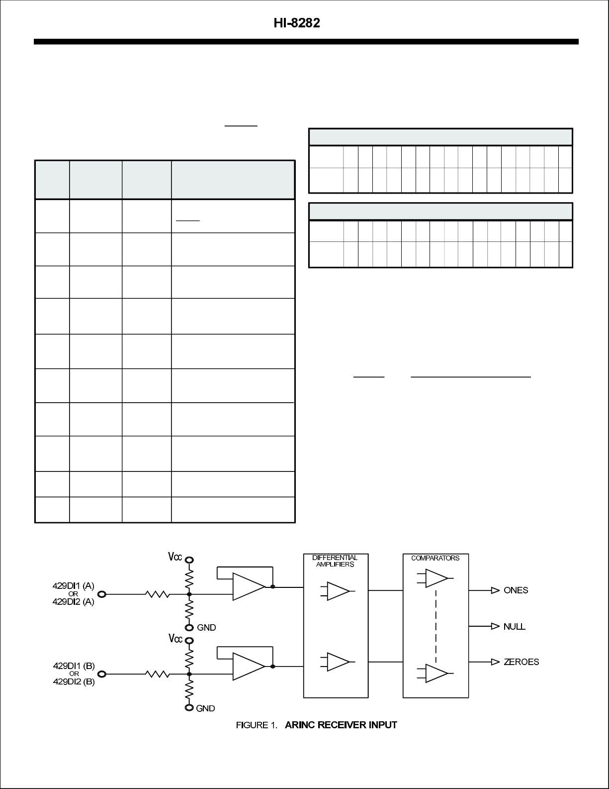
Figure1showstheinputcircuitforeachreceiver.TheARINC429
specificationrequiresthefollowingdetectionlevels:
STATEDIFFERENTIALVOLTAGE
ONE+6.5Voltsto+13Volts
NULL+2.5Voltsto-2.5Volts
ZERO-6.5Voltsto-13Volts
TheHI-8282guaranteesrecognitionoftheselevelswithacommon
modeVoltagewithrespecttoGNDlessthan±4Vfortheworstcase
condition(4.75Vsupplyand13vsignallevel).
Thetolerancesinthedesignguaranteedetectionoftheabove
levels,sotheactualacceptancerangesareslightlylarger.Ifthe
ARINCsignalisoutoftheactualacceptanceranges,includingthe
nulls,thechiprejectsthedata.
HOLTINTEGRATEDCIRCUITS
4-31
HI-8282
FUNCTIONALDESCRIPTION(con't)
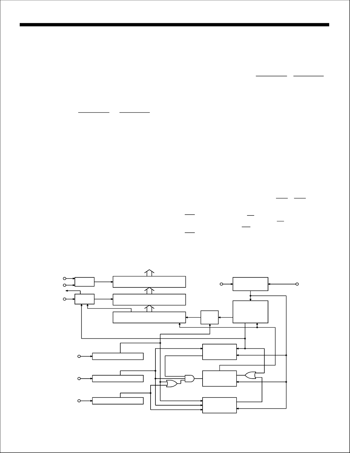
RECEIVERLOGICOPERATION
Figure2showsablockdiagramofthelogicsectionofeachreceiver.
BITTIMING
TheARINC429specificationcontainsthefollowingtiming
specificationforthereceiveddata:
HIGHSPEEDLOWSPEED
BITRATE
PULSERISETIME
PULSEFALLTIME
PULSEWIDTH
AgaintheHI-8282acceptssignalsthatmeetthesespecifications
andrejectsoutsidethetolerances.Thewaythelogicoperation
achievesthisisdescribedbelow:
1.Keytotheperformanceofthetimingcheckinglogicisanaccurate1MHzclocksource.Lessthan0.1%erroris
recommmended.
2.Thesamplingshiftregistersare10bi tslongandmustshow
threeconsecutiveOnes,ZerosorNullstobeconsideredvalid
data.Additionally,fordatabits,theOneorZerointheupperbits
ofthesamplingshiftregistersmustbefollowedbyaNullinthe
lowerbitswithinthedatabittime.ForaNullinthewordgap,
threeconsecutiveNullsmustbefoundinboththeupperand
lowerbitsofthesamplingshiftregister.Inthismannertheminimumpulsewidthisguaranteed.
100KBPS±1%12K-14.5KBPS
1.5±0.5µsec10±5µsec
1.5±0.5µsec10±5µsec
5µsec±5%34.5to41.7µsec
TOPINS
3.Eachdatabitmustfollowitspredecessorbynotlessthan
8samplesandnomorethan12samples.Inthismannerthe
bitrateischecked.Withexactly1MHzinputclockfrequency,
theacceptabledatabitratesareasfollows:
HIGHSPEEDLOWSPEED
DATABITRATEMIN
DATABITRATEMAX
83KBPS10.4KBPS
125KBPS15.6KBPS
4.TheWordGaptimersamplestheNullshiftregisterevery
10inputclocks(80forlowspeed)afterthelastdatabitofa
validreception.IftheNullispresent,theWordGapcounteris
incremented.Acountof3willenablethenextreception.
RECEIVERPARITY
ThereceiverparitycircuitcountsOnesreceived,includingthe
paritybit,ARINCbit32.Iftheresu ltisodd,then"0"willappearin
the32ndbit.
RETRIEVINGDATA
Once32validbitsarerecognized,thereceiverlogicgenerates
anEndofSequence(EOS).Ifthereceiverdecoderisenabled
andthe9thand10thARINCbitsmatchthecontrolword
programbitsorifthereceiverdecoderisdisabled,thenEOS
clocksthedatareadyflagflipfloptoa"1",or(orboth)
D/R1D/R2
willgolow.Thedataflagforareceiverwillremainlowuntilafter
ARINCbytesfromthatreceiverareretrieved.Thisis
both
accomplishedbyactivatingwithSEL,thebyteselector,low
toretrievethefirstbyteandactivatingwithSELhighto
retrievethesecondbyte.retrievesdatafromreceiver1and
ret rievesdatafromreceiver2.
EN2
EN
EN
ENI
IfanotherARINCwordisreceived,andanewEOSoccurs
beforethetwobytesareretrieved,thedataisoverwrittenbythe
newword.
DECODER
CONTROL
BITS
SEL
EN
D/R
ZEROS
ONES
NULL
MUX
CONTROL
LATCH
ENABLE
/
CONTROL
BITS9&10
EOS
SHIFTREGISTER
SHIFTREGISTER
SHIFTREGISTER
32TO16DRIVER
32BITLATCH
32BITSHIFTREGISTER
DATA
BITCLOCK
WORDGAP
START
CONTROL
BITBD14
PARITY
CHECK
WORDGAP
SEQUENCE
CONTROL
DETECTION
TIMER
ERROR
32ND
CLOCK
OPTION
CLOCK
BIT
COUNTER
AND
BIT
SEQUENCE
EOS
BITCLOCK
END
ERROR
CLOCK
ENDOF
CLK
FIGURE2. RECEIVERBLOCKDIAGRAM
HOLTINTEGRATEDCIRCUITS
4-32
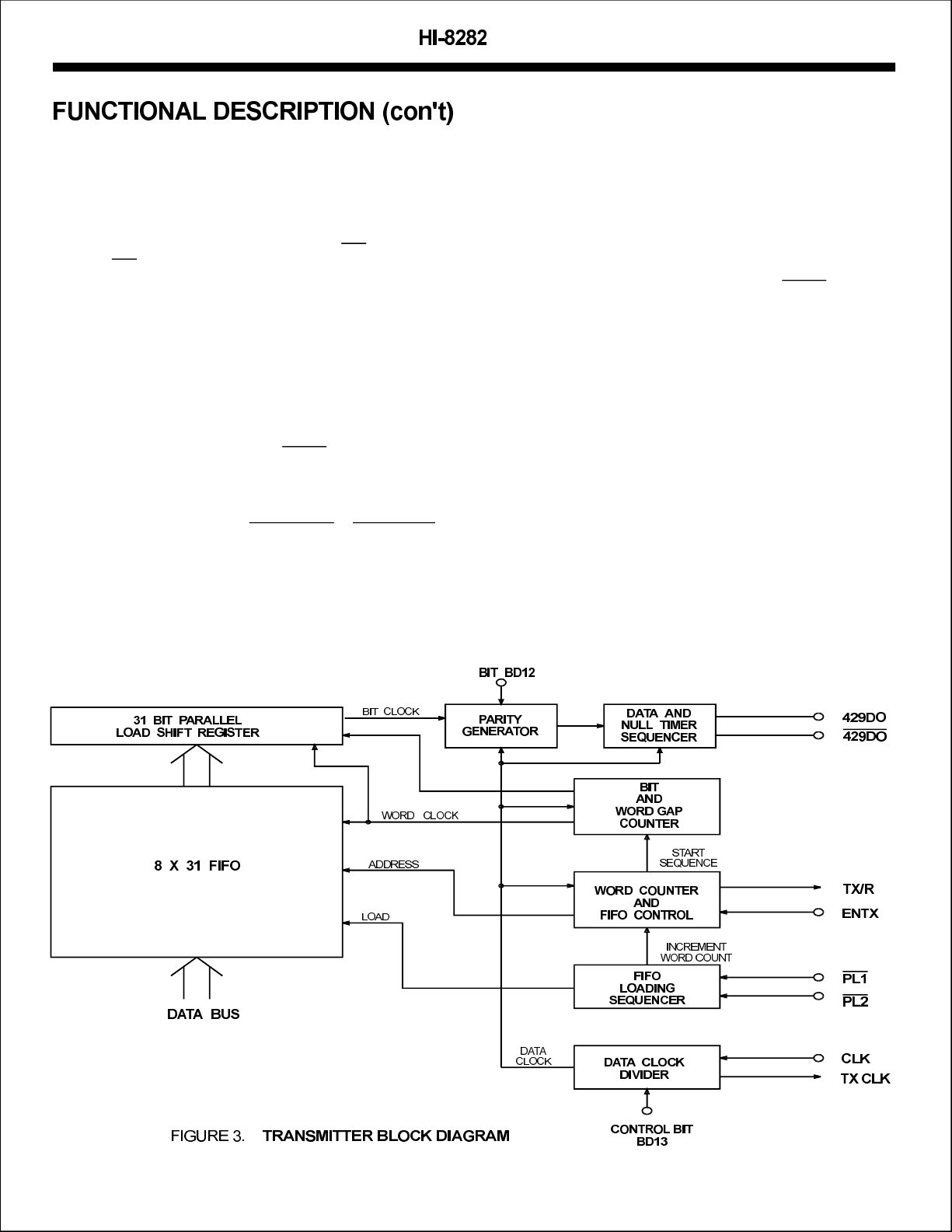
TRANSMITTER
TRANSMITTERPARITY
AblockdiagramofthetransmittersectionisshowninFigure3.
FIFOOPERATION
TheFIFOisloadedsequentiallybyfirstpulsingtoloadbyte1
andthentoloadbyte2.Thecontrollogicautomaticallyloads
the31bitwordinthenextavailablepositionoftheFIFO.IfTX/R,
thetransmitterreadyflagishigh(FIFOempty),then8words,
each31bitslong,maybeloaded.IfTX/Rislow,thenonlythe
availablepositionsmaybeloaded.Ifall8positionsarefull,the
FIFOignoresfurtherattemptstoloaddata.
PL2
PL1
DATATRANSMISSION
WhenENTXgoeshigh,enablingtransmission,theFIFO
positionsareincrementedwiththetopregisterloading intothe
datatransmissionshiftregister.Within2.5dataclocksthefirst
databitappearsateither429DOor.The31bitsinthe
datatransmissionshiftregisterarepresentedsequentiallytothe
outputsintheARINC429formatwiththefollowingtiming:
ARINCDATABITTIME10Clocks80Clocks
DATABITTIME5Clocks40Clocks
NULLBITTIME5Clocks40Clocks
WORDGAPTIME40Clocks320Clocks
Thewordcounterdetectswhenallloadedpositionsare
transmittedandsetsthetransmitterreadyflag,TX/R,high.
429DO
HIGHSPEEDLOWSPEED
TheparitygeneratorcountstheONESinthe31-bitword.Ifthe
BD12controlwordbitissetlow,the32ndbittransmittedwillmake
parityodd.Ifthecontrolbitishightheparityiseven.
SELFTEST
IftheBD05controlwordbitissetlow,429DOorbecome
inputstothereceiverbypassingtheinterfacecircuitry.
429DO
SYSTEMOPERATION
Thetworeceiversareindependentofthetransmitter.Therefore,
controlofdataexchangesarestrictlyattheoptionoftheuser.The
onlyrestrictionsare:
1.Thereceiveddatamaybeoverwrittenifnotretrieved
withinoneARINCwordcycle.
2.TheFIFOcanstore8wordsmaximumandignores
attemp tstoloadadditiondataiffull.
3.Byte1ofthetransmitterdatamustbeloadedfirst.
4.Eitherbyteofthereceiveddatamayberetrievedfirst.
Bothbytesmustberetrievedtoclearthedatareadyflag.
5.AfterENTX,transmissionenable,goeshighitcannotgo
lowuntilTX/R,transmitterreadyflag,goeshigh.Otherwise,
oneARINCwordislostduringtransmission.
HOLTINTEGRATEDCIRCUITS
4-33
 Loading...