

Datasheet HI-8282ACLT, HI-8282ACLM, HI-8282ACLI, HI-8282ACDT, HI-8282ACDI Datasheet (HOLT)
...
HI-8282A
ARINC429SERIALTRANSMITTERANDDUALRECEIVER
PINCONFIGURATION (TopView)
GENERALDESCRIPTION
TheHI-8282AisasilicongateCMOSdeviceforinterfacing
theARINC429serialdatabustoa16-bitparalleldatabus.
Tworeceiversandanindependenttransmitterare
provided.Thereceiverinputcircuitryandlogicare
designedtomeettheARINC429specificationsforloading,
leveldetection,timing,andprotocol.Thetransmitter
sectionprovidestheARINC429communicationprotocol.
AdditionalinterfacecircuitrysuchastheHoltHI-8585,
HI-8586orHI-3182isrequiredtotranslatethe5voltlogic
outputstoARINC429drivelevels.
The16-bitparalleldatabusexchangesthe32-bi tARINC
datawordintwostepswheneitherloadingthetransmitter
orinterrogatingthereceivers.Thedatabusinterfaceswith
CMOSandTTL.
Timingofallthecircuitrybeginswiththemasterclockinput,
CLK.ForARINC429applications,themasterclock
frequencyis1MHz.
Eachindependentreceivermonitorsthedatastreamwitha
samplingrate10timesthedatarate.Thesamplingrateis
softwareselectableateither1MHzor125KHz.Theresults
ofaparitycheckareavailableasthe32ndARINCbit.The
HI-8282Aexaminesthenullanddatatimingsandwillreject
erroneouspatterns.Forexample ,witha125KHzclock
selection,thedatafrequencymustbebetween10.4KHz
and15.6KHz.
ThetransmitterhasaFirstIn,FirstOut(FIFO)memoryto
store8ARINCwordsfortransmission.Thedatarateofthe
transmitterissoftwareselectablebydividingthemaster
clock,CLK,byeither10or80.Themasterclockisusedto
setthetimingoftheARINCtransmissionwithintherequired
resolution.
APPLICATIONS
!
!
!
Avionicsdatacommunication
Serialtoparallelconversion
Paralleltoserialconversion
FEATURES
!
!
!
!
!
!
!
!
!
!
!
ARINCspecification429compatible
16-Bitparalleldatabus
DirectreceiverinterfacetoARINCbus
Timingcontrol10timesthedatarate
Selectabledataclocks
ReceivererrorrejectionperARINC
specification429
Automatictransmitterdatatiming
Selftestmode
Parityfunctions
Lowpower,single5voltsupply
Industrial&fullmilitarytemperatureranges
HOLTINTEGRATEDCIRCUITS
1(DS8282ARev.New) 05/01
May2001
44-PinPlasticQuadFlatPack(PQFP)
(Seepage10foradditionalPackagePinConfigurations)
33-N/C
32-N/C
3130-ENTX
2928-429DO
27-TX/R
262524-BD00
23-BD01
CWSTRX
429DO
PL2
PL1
N/C-1
-2
-3
SEL-4
-5
-6
BD15-7
BD14-8
BD13-9
BD12-10
BD11-11
D/R1
D/R2
EN1
EN2
HI-8282APQI
&
HI-8282APQT

SYMBOLFUNCTIONDESCRIPTION
VCCPOWER+5V±5%
429DI1(A)INPUTARINCreceiver1positiveinput
429DI1(B)INPUTARINCreceiver1negativeinput
429DI2(A)INPUTARINCreceiver2positiveinput
429DI2(B)INPUTARINCreceiver2negativeinput
OUTPUTReceiver1datareadyflag
OUTPUTReceiver2datareadyflag
SELINPUTReceiverdatabyteselection(0=BYTE1)(1=BYTE2)
INPUTDataBuscontrol,enablesreceiver1datatooutputs
INPUTDataBuscontrol,enablesreceiver2datatooutputsifishigh
BD15I/ODataBus
BD14I/ODataBus
BD13I/ODataBus
BD12I/ODataBus
BD11I/ODataBus
BD10I/ODataBus
BD09I/ODataBus
BD08I/OData Bus
BD07I/ODataBus
BD06I/ODataBus
GNDPOWER0V
BD05I/ODataBus
BD04I/ODataBus
BD03I/ODataBus
BD02I/ODataBus
BD01I/ODataBus
BD00I/ODataBus
INPUTLatchenableforbyte1enteredfromdatabustotransmitterFIFO.
INPUTLatchenableforbyte2enteredfromdatabustotransmitterFIFO.Mustfollow
TX/ROUTPUTTransmitterreadyflag.GoeslowwhenARINCwordloadedintoFIFO.Goeshigh
aftertransmissionandFIFOempty.
429DOOUTPUT"ONES"dataoutputfromtransmitter.
OUTPUT"ZEROES"dataoutputfromtransmitter.
ENTXINPUTEnableTransmission
INPUTClockforcontrolwordregiste r
CLKINPUTMasterClockinput
TXCLKOUTPUTTransmitterClockequaltoMasterClock(CLK),dividedbyeither10or80.
INPUTMasterReset,activelow
D/R1
D/R2
EN1
EN2EN1
PL1
PL2PL1.
429DO
CWSTR
MR
PINDESCRIPTION
HI-8282A
HOLTINTEGRATEDCIRCUITS
2

HI-8282A
FUNCTIONALDESCRIPTION
DATA
BUSFUNCTIONCONTROLDESCRIPTION
PIN
Ifenabled,aninternalconnection
BDO5SELFTEST0=ENABLEismadepassing429DOand
tothereceiverlogicinputs
RECEIVER1Ifenabled,ARINCbits9and,
BDO6DECODER1=ENABLE10mustmatchthenexttwo
controlwordbits
IfReceiver1Decoderis
BDO7--enabled,theARINCbit9
mustmatchthisbit
IfReceiver1Decoderis
BDO8--enabled,theARINCbit10
mustmatchthisbit
RECEIVER2Ifenabled,ARINCbits9and
BDO9DECODER1=ENABLE10mustmatchthenexttwo
controlwordbits
IfReceiver2Decoderis
BD10--enabled,thenARINCbit9
mustmatchthisbit
IfReceiver2Decoderis
BD11--enabled,thenARIN Cbit10
mustmatchthisbit
INVERTLogic0enablesnormaloddparity
BD12XMTR1=ENABLEandLogic1enablesevenparity
PARITYoutputintransmitter32ndbit
BD13XMTRDATA0=÷10CLKisdividedeitherby10or
CLKSELECT1=÷8080toobtainXMTRdataclock
BD14RCVRDTA0=÷10CLKisdividedeitherby10or
CLKSELECT1=÷8080toobtainRCVRdataclock
429DO
CONTROLWORDREGISTER
TheHI-8282Acontains10dataflipflopswhoseDinputsareconnectedtothedatabusandclocksconnectedto.Each
flipflopprovidesoptionstotheuserasfollows:
CWSTR
THERECEIVERS
ARINCBUSINTERFACE
Figure1showstheinputcircuitforeachreceiver.TheARINC429
specificationrequiresthefollowingdetectionlevels:
TheHI-8282Aguaranteesrecognitionoftheselevelswithacommon
modeVoltagewithrespecttoGNDlessthan±5Vfortheworstcase
condition(4.75Vsupplyand13vsignallevel).
Thetolerancesinthedesignguaranteedetectionoftheabove
levels,sotheactualacceptancerangesareslightlylarger.Ifthe
ARINCsignalisoutoftheactualacceptanceranges,includingthe
nulls,thechiprejectsthedata.
STATEDIFFERENTIALVOLTAGE
ONE+6.5Voltsto+13Volts
NULL+2.5Voltsto-2.5Volts
ZERO-6.5Voltsto-13Volts
BYTE2
DATABDBDBDBDBDBDBDBDBDBDBDBDBDBDBDBD
BUS15141312111009080706050403020100
ARINC29282726252423222120191817161514
BIT
ARINC429DATAFORMAT
Thefollowingtableshowsthebitpositionsinexchangingdatawith
thereceiverorthetransmitter.ARINCbit1isthefirstbit
transmittedorreceived.
DATABDBDBDBDBDBDBDBDBDBDBDBDBDBDBDBD
BUS15141312111009080706050403020100
ARINC13121110931303212345678
BIT
BYTE1
HOLTINTEGRATEDCIRCUITS
3
HI-8282A
RECEIVERLOGICOPERATION
BITTIMING
BITRATE
PULSERISETIME
PULSEFALLTIME
PULSEWIDTH
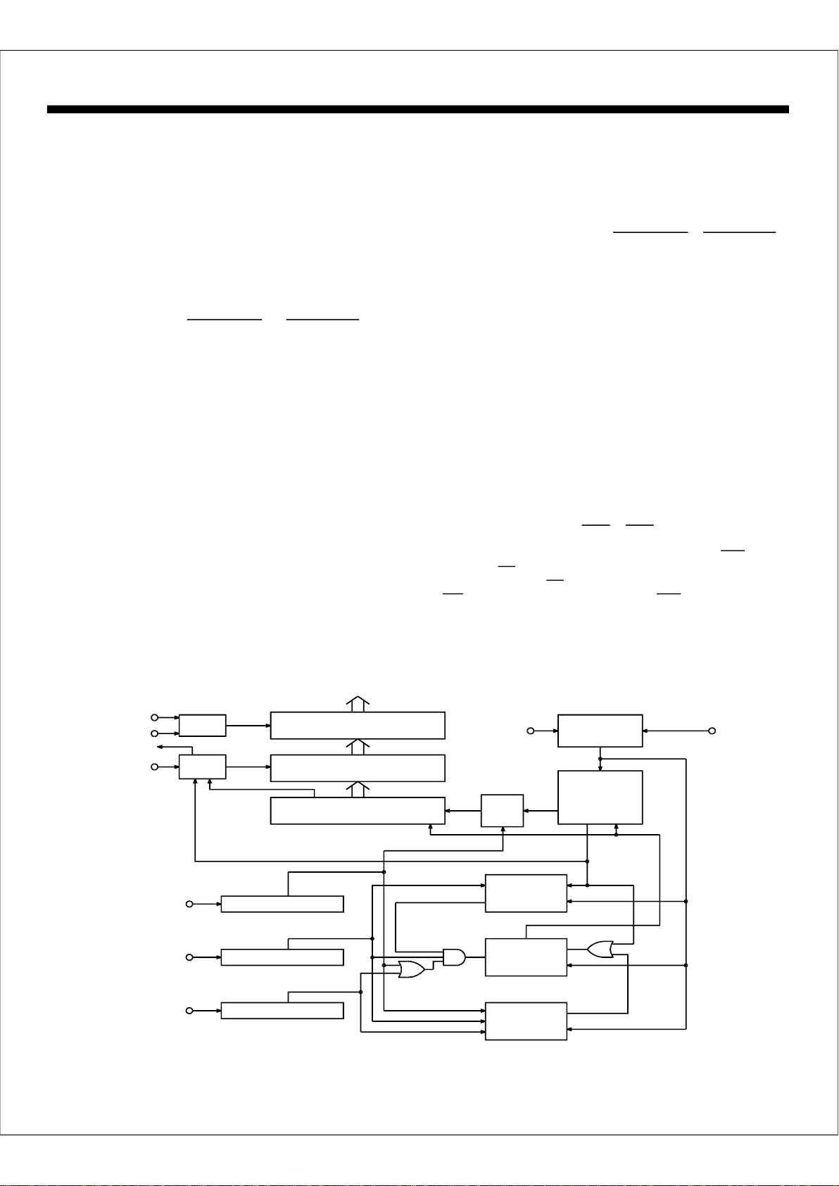
Figure2showsablockdiagramofthelogicsectionofeachreceiver.
TheARINC429specificationcontainsthefollowingtiming
specificationforthereceiveddata:
100KBPS±1%12K-14.5KBPS
1.5±0.5µsec10±5µsec
1.5±0.5µsec10±5µsec
5µsec±5%34.5to41.7µsec
AgaintheHI-8282Aacceptssignalsthatmeetthesespecifications
andrejectsoutsidethetolerances.Thewaythelogicoperation
achievesthisisdescribedbelow:
1.Keytotheperformanceofthetimingcheckinglogicisanaccurate1MHzclocksource.Lessthan0.1%erroris
recommmended.
2.Thesamplingshiftregistersare10b itslongandmustshow
threeconsecutiveOnes,ZerosorNullstobeconsideredvalid
data.Additionally,fordatabits,theOneorZerointheupperbits
ofthesamplingshiftregistersmustbefollowedbyaNullinthe
lowerbitswithinthedatabittime.ForaNullinthewordgap,
threeconsecutiveNullsmustbefoundinboththeupperand
lowerbitsofthesamplingshiftregister.Inthismannertheminimumpulsewidthisguaranteed.
HIGHSPEEDLOWSPEED
FUNCTIONALDESCRIPTION(con't)
3.Eachdatabitmustfollowitspredecessorbynotlessthan
8samplesandnomorethan12samples.Inthismannerthe
bitrateischecked.Withexactly1MHzinputclockfrequency,
theacceptabledatabitratesareasfollows:
83KBPS10.4KBPS
125KBPS15.6KBPS
4.TheWordGaptimersamplestheNullshiftregisterevery
10inputclocks(80forlowspeed)afterthelastdatabitofa
validreception.IftheNullispresent,theWordGapcounteris
incremented.Acountof3willenablethenextreception.
ThereceiverparitycircuitcountsOnesreceived,includingthe
paritybit,ARINCbit32.Iftheresu ltisodd,then"0"willappearin
the32ndbit.
HIGHSPEEDLOWSPEED
DATABITRATEMIN
DATABITRATEMAX
RECEIVERPARITY
RETRIEVINGDATA
Once32validbitsarerecognized,thereceiverlogicgeneratesan
EndofSequence(EOS).Ifthereceiverdecoderisenabledand
the9thand10thARINCbitsmatchthecontrolwordprogrambits
orifthereceiverdecoderisdisabled,thenEOSclocksthedata
readyflagflipfloptoa"1",or(orboth)willgolow.The
dataflagforareceiverwillremainlowuntilafterARINC
bytesfromthatreceiverareretrieved.Thisisaccomplishedby
activatingwithSEL,thebyteselector,lowtoretrievethefirst
byteandactivatingwithSELhightoretrievethesecondbyte.
retrievesdatafromreceiver1andret rievesdatafrom
receiver2.
IfanotherARINCwordisreceived,andanewEOSoccursbefore
thetwobytesareretrieved,thedataisoverwrittenbythenew
word.
D/R1D/R2
EN
EN
ENIEN2
both
SEL
EN
D/R
DECODER
CONTROL
BITS
/
MUX
CONTROL
LATCH
ENABLE
CONTROL
32TO16DRIVER
32BITLATCH
32BITSHIFTREGISTER
TOPINS
CONTROL
BITBD14
CLOCK
OPTION
CLOCK
CLK
BIT
COUNTER
AND
ENDOF
SEQUENCE
PARITY
CHECK
32ND
BIT
DATA
BITCLOCK
EOS
WORDGAP
WORDGAP
TIMER
BITCLOCK
END
START
SEQUENCE
CONTROL
ERROR
CLOCK
ERROR
DETECTION
SHIFTREGISTER
SHIFTREGISTER
NULL
ZEROS
SHIFTREGISTER
ONES
EOS
BITS9&10
FIGURE2. RECEIVERBLOCKDIAGRAM
HOLTINTEGRATEDCIRCUITS
4
HI-8282A
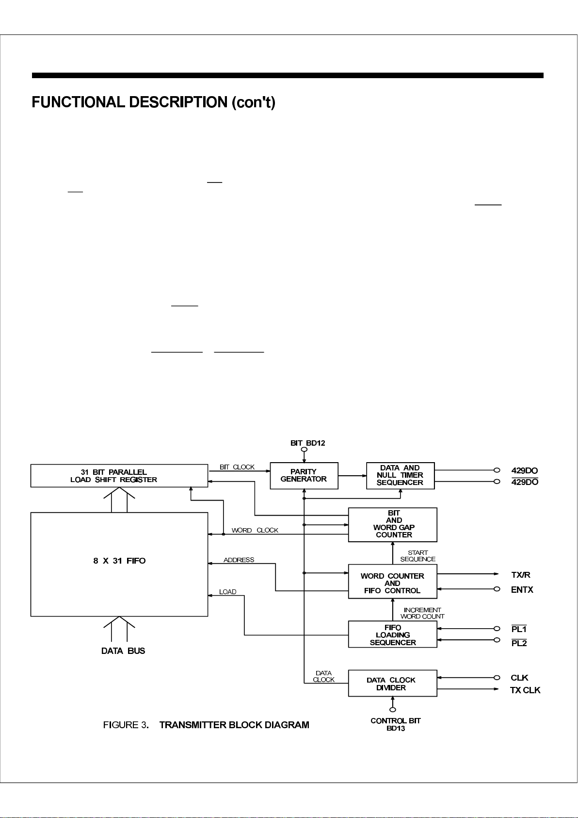
TRANSMITTER
AblockdiagramofthetransmittersectionisshowninFigure3.
TheFIFOisloadedsequentiallybyfirstpulsingtoloadbyte1
andthentoloadbyte2.Thecontrollogicautomaticallyloads
the31bitwordinthenextavailablepositionoftheFIFO.IfTX/R,
thetransmitterreadyflagishigh(FIFOempty),then8words,
each31bitslong,maybeloaded.IfTX/Rislow,thenonlythe
availablepositionsmaybeloaded.Ifall8positionsarefull,the
FIFOignoresfurtherattemptstoloaddata.
WhenENTXgoeshigh,enablingtransmission,theFIFO
positionsareincrementedwiththetopregisterloading intothe
datatransmissionshiftregister.Within2.5dataclocksthefirst
databitappearsateither429DOor.The31bitsinthe
datatransmissionshiftregisterarepresentedsequentiallytothe
outputsintheARINC429formatwiththefollowingtiming:
ARINCDATABITTIME10Clocks80Clocks
DATABITTIME5Clocks40Clocks
NULLBITTIME5Clocks40Clocks
WORDGAPTIME40Clocks320Clocks
Thewordcounterdetectswhenallloadedpositionsare
transmittedandsetsthetransmitterreadyflag,TX/R,high.
FIFOOPERATION
DATATRANSMISSION
PL1
PL2
429DO
HIGHSPEEDLOWSPEED
TRANSMITTERPARITY
TheparitygeneratorcountstheONESinthe31-bitword.Ifthe
BD12controlwordbitissetlow,the32ndbittransmittedwillmake
parityodd.Ifthecontrolbitishightheparityiseven.
IftheBD05controlwordbitissetlow,429DOorbecome
inputstothereceiverbypassingtheinterfacecircuitry.
Thetworeceiversareindependentofthetransmitter.Therefore,
controlofdataexchangesarestrictlyattheoptionoftheuser.The
onlyrestrictionsare:
1.Thereceiveddatamaybeoverwrittenifnotretrieved
withinoneARINCwordcycle.
2.TheFIFOcanstore8wordsmaximumandignores
attemp tstoloadadditiondataiffull.
3.Byte1ofthetransmitterdatamustbeloadedfirst.
4.Eitherbyteofthereceiveddatamayberetrievedfirst.
Bothbytesmustberetrievedtoclearthedatareadyflag.
5.AfterENTX,transmissionenable,goeshighitcannotgo
lowuntilTX/R,transmitterreadyflag,goeshigh.Otherwise,
oneARINCwordislostduringtransmission.
SELFTEST
SYSTEMOPERATION
429DO
HOLTINTEGRATEDCIRCUITS
5

REPEATEROPERATION
Therepeatermodeofoperationallowsadatawordthathasbeen
receivedbytheHI-8282AtobeplaceddirectlyintoitsFIFOfor
transmission.Aftera32-bitwordhasbeenshiftedintothereceiver
shiftregister,theflagwillgolow.Alogic"0"isplacedontheSEL
lineandisstrobed.Thisisthesameprocedureasfornormal
receiveroperationanditplacesthelowerbyte(16)ofthedataword
onthedatabus.Bystrobingatthesame
D/R
EN
PL1 timeas,thebyteEN
HI-8282A
willalsobeplacedintothetransmitterFIFO.SEListhentakenhigh
andisstrobedagaintoplacetheupperbyteofthedatawordon
thedatabus.Bystrobingatthesametimeas,thesecond
bytewillalsobeplacedintotheFIFO.Thedatawordisnowreadyto
betransmittedaccordingtotheparityprogrammedintothecontrol
wordregister.
Innormaloperation,eitherbyteofareceiveddatawordmayberead
fromthereceiverlatchesfirstbyuseofSELinput.Duringrepeater
operationhowever,thelowerbyteofthedatawordmustberead
first.Thisisnecessarybecause,asthedataisbeingread,itisal so
beingloadedintotheFIFOandthetransmitterFIFOisalways
loadedwiththelowerbyteofthedatawordfirst.
EN
PL2EN
429DO
429DO
ARINCBIT
NULL
DATA
DATA
DATA
NULL
NULL
WORDGAP
BIT1
NEXTWORD
BIT32
BIT31
BIT30
CWHLD
t
CWSET
t
CWSTR
t
DATABUS
CWSTR
VALID
DATABUS
SELEN
t
D/R
t
ENSEL
t
DATAEN
t
D/REN
t
END/R
t
EN
t
ENSEL
t
SELEN
t
DATAEN
t
ENDATA
t
ENDATA
t
ENEN
t
BYTE1VALID BYTE2VALID
HOLTINTEGRATEDCIRCUITS
6

HI-8282A
PL2
DWSET
t
DWHLD
t
TX/R
t
DWHLD
t
PL12
t
PL
t
DATABUS
PL1
TX/R
BYTE2VALID
PL
t
PL12
t
DWSET
t
BYTE1VALID
ARINCBIT
429DO
or
429DO
PL2
ENTX
TX/R
PL2EN
t
ENDAT
t
DTX/R
t
ENTX/R
t
DATA
BIT1
DATA
BIT2
DATA
BIT32
DON'TCARE
429DI
D/R
EN
PL1
PL2
SEL
TX/R
ENTX
429DO
BIT32
DON'TCARE
D/R
t
EN
t
D/REN
t
ENEN
t
EN
t
END/R
t
SELEN
t
ENSEL
t
ENPL
t
PLEN
t
SELEN
t
ENSEL
t
ENPL
t
PLEN
t
TX/R
t
TX/REN
t
ENDAT
t
ENTX/R
t
DTX/R
t
NULL
t
BIT1 BIT32
HOLTINTEGRATEDCIRCUITS
7

OperatingSupplyCurrent:I20mACC2
StandbySupplyCurrent:I20mACC1
SUPPLYINPUT-V CC
OutputCapacitance:C15pFO
(AllOtherOutputs)OutputSourceIV=V-0.4V1.1mAOHOUTCC
OutputCurrent:OutputSinkIV=0.4V2.6mAOLOUT
(Bi-directionalPins)OutputSourceIV=V-0.4V1.1mAOHOUTCC
OutputCurrent:OutputSinkIV=0.4V3.0mAOLOUT
Logic"0"OutputVoltageVI=1.1mA0.4VOLOL
OutputVoltage:Logic"1"OutputVoltageVI=-1.5mA2.7VOHOH
OUTPUTS-,,BD00throughBD15,TX/R,429DO,&TXCLKD/R1D/R2429DO
InputSourceI-20µAIL
InputCurrent:InputSinkI10µAIH
InputVoltageLOV0.7VIL
InputVoltage:InputVoltageHIV3.5VIH
ALLOTHERINPUTS-SEL,,,,,ENTX,EN1EN2 PL1PL2CWSTRMR,CLK&
InputSourceI-1.5µAIL
InputCurrent:InputSinkI1.5µAIH
InputVoltageLOV0.7VIL
InputVoltage:InputVoltageHIV2.1VIH
BI-DIRECTIONALINPUTS-BD00throughBD15
ToVccC20pFH
(Guaranteedbutnottested)ToGNDC20pFG
InputCapacitance:DifferentialCPins2to3,4to520pFI
InputSourceI-450µAIL
InputCurrent:InputSinkI200µAIH
ToVccR1227KH Ω
ToGNDR1227KG Ω
InputResistance:DifferentialR12KI Ω
NULLVwithrespecttoGND-2.502.5VNUL
ZEROVmodevoltagelessthan±5V-13.0-10.0-6.5VIL
DifferentialInputVoltage:ONEVARINCInputPins:Common6.510.013.0VIH
ARINCINPUTS-429DI1(A),429DI1(B),429DI2(A)&429DI2(B)
MINTYPMAX
PARAMETERCONDITIONSUNITSYMBOL LIMITS
Vcc=5V±5%,GND=0V,TA=OperatingTemperatureRange(unlessotherwisespecified).
PowerDissipation500mW
OperatingTemperatureRange:(Industrial)-40°Cto+85°C
(Military)-55°Cto+125°C
StorageTemperatureRange:-65°Cto+150°C
SupplyVoltageVcc-0.3Vto+7V
VoltageatARINCInputs-29Vto+29V
Voltageatanyotherpin-0.3VtoVcc+0.3V
DCCurrentDrainperinputpin10mA
NOTE:Stressesabovethoselistedunder"AbsoluteMaximumRatings"maycausepermanentdamagetothedevice.Thesea restressratingsonly.
Functionaloperationofthedeviceattheseoranyotherconditionsabovethoseindicatedintheoperationalsection softhespecificationsisnotimplied.
Exposuretoabsolutemaximumratingconditionsforextendedperiodsmayaffectdevicereliability.
HI-8282A
HOLTINTEGRATEDCIRCUITS
8

LIMITS
PARAMETERSYMBOLUNITS
MINTYPMAX
CONTROLWORDTIMING
RECEIVERTIMING
FIFOTIMING
TRANSMISSIONTIMING
REPEATEROPERATIONTIMING
MasterResetPulseWidth
ARINCDataRateandBitTiming
PulseWidth-t130ns
Setup-DATABUSValidtoHIGHt130ns
Hold-HIGHtoDATABUSHi-Zt0ns
Delay-StartARINC32ndBittoLOW:HighSpeedt16µs
LowSpeedt128µs
Delay-LOWtoL0Wt0ns
Delay-LOWtoHIGHt200ns
Setup-SELtoL0Wt20ns
Hold-SELtoHIGHt20ns
Delay-L0WtoDATABUSValidt200ns
Delay-HIGHtoDATABUSHi-Zt30ns
PulseWidth-ort200ns
Spacing-HIGHtonextL0Wt50ns
PulseWidth-ort200ns
Setup-DATABUSValidtoHIGHt110ns
Hold-HIGHtoDATABUSHi-Zt0ns
Spacing-ort0ns
Delay-HIGHtoTX/RLOWt840ns
Spacing-HIGHtoENTXHIGHt0µs
Delay-ENTXHIGHto429DOor:HighSpeedt25µs
Delay-ENTXHIG Hto429DOor:LowSpeedt200µs
Delay-32ndARINCBittoTX/RHIGHt400ns
Spacing-TX/RHIGHtoENTXL0Wt0ns
Delay-LOWtoLOWt0ns
Hold-HIGHtoHIGHt0ns
Delay-TX/RLOWtoENTXHIGHt0ns
t200ns
±1%
CWSTR
CWSTR
CWSTR
D/R
D/REN
END/R
EN
EN
EN
EN
EN1EN2
ENEN
PL1PL2
PL
PL
PL1PL2
PL2
PL2
429D0
429D0
ENPL
PLEN
CWSTR
CWSET
CWHLD
D/R
D/R
D/REN
END/R
SELEN
ENSEL
ENDATA
DATAEN
EN
ENEN
PL
DWSET
DWHLD
PL12
TX/R
PL2EN
ENDAT
ENDAT
DTX/R
ENTX/R
ENPL
PLEN
TX/REN
MR
HI-8282A
HOLTINTEGRATEDCIRCUITS
9
Vcc=5V,GND=0V,TA=OperatingTemperatureRangeandfclk=1MHz0.1%with60/40dutycycle+

HI-8282A
ADDITIONALHI-8282APINCONFIGURATIONS
(Seepage1forthe44-pinPlasticQuadFlatPack)
HOLTINTEGRATEDCIRCUITS
10
HI-8282APJI
HI-8282ACRI
44-PINJ-LEADCERQUAD
44-PINCERAMICLCC
HI-8282ACLI
40-PINCERAMICSIDEBRAZEDDIP
44-PINPLASTICPLCC
HI-8282ACDI

PART
NUMBER
PACKAGE
DESCRIPTION
TEMPERATURE
RANGE
FLOW
BURN INLEAD
FINISH
HI-8282ACDI 40 PIN CERAMIC SIDE BRAZED DIP -40°C TO +85°C I NO GOLD
HI-8282ACDT 40 PIN CERAMIC SIDE BRAZED DIP -55°C TO +125°C T NO GOLD
HI-8282ACDM 40 PIN CERAMIC SIDE BRAZED DIP -55°C TO +125°C M YES SOLDER
HI-8282APJI 44 PIN PLASTIC J LEAD -40°C TO +85°C I NO SOLDER
HI-8282APJT 44 PIN PLASTIC J LEAD -55°C TO +125°C T NO SOLDER
HI-8282APQI 44 PIN PLASTIC QUAD FLAT PACK -40°C TO +85°C I NO SOLDER
HI-8282APQT 44 PIN PLASTIC QUAD FLAT PACK -55°C TO +125°C T NO SOLDER
HI-8282ACLI 44 PIN CERAMIC LEADLESS CHIP CARRIER -40°C TO +85°C I NO GOLD
HI-8282ACLT 44 PIN CERAMIC LEADLESS CHIP CARRIER -55°C TO +125°C T NO GOLD
HI-8282ACLM 44 PIN CERAMIC LEADLESS CHIP CARRIER -55°C TO +125°C M YES SOLDER
HI-8282ACRI 44 PIN CERQUAD -40°C TO +85°C I NO SOLDER
HI-8282ACRT 44 PIN CERQUAD -55°C TO +125°C T NO SOLDER
HI-8282A
HOLTINTEGRATEDCIRCUITS
11

PackageType:
214443
.620 ± .012
(15.748 ± .305)
.688 ± .005
(17.475 ± .127)
MAX.
SQ.
.650 ± .010
(16.510 ± .254)
SQ.
.200
(5.080)
MAX.
.050
(1.270)
.019 ± .002
(.483 ± .051)
.100 ± .007
(2.540 ± .178)
TYP.
44-PINJ-LEADCERQUAD
44U
.039 ± .005
(.990 ± .127)
PackageType:
2.020MAX
(51.308MAX)
.225MAX
(5.715MAX)
.100BSC
(2.540BSC)
.018TYP
(.457TYP)
.050TYP
(1.270TYP)
.085 ± .009
(2.159 ± .229)
.125MIN
(3.175MIN)
.610 ± .010
(15.494 ± .254)
.600 ± .010
(15.240 ± .254)
.595 ± .010
(15.113 ± .254)
.010 + .002 /− .001
(.254 + .051 /− .025)
40-PINCERAMICSIDE-BRAZEDDIP
40C
HI-8282APACKAGEDIMENSIONS
inches(millimeters)
HOLTINTEGRATEDCIRCUITS
12

PackageType:
PINNO.1IDENT
.045x45°
.050 ± .005
(1.27 ± .127)
.045x45°
PINNO.1
44-PINPLASTICPLCC
SEEDETAIL
A
.172 ± .008
(4.369 ± .203)
DETAILA
.020MIN
(.508 ΜΙΝ )
.025
.045
R
.690 ± .005
(17.526 ± .127)
SQ.
.610 ± .020
(15.494 ± .508)
.031 ± .005
(.787 ± .127)
.653 ± .004
(16.586 ± .102)
SQ.
.017 ± .004
(.432 ± .102)
.015±.002
(.381 ± .051)
.009
.011
44J
HI-8282APACKAGEDIMENSIONS
inches(millimeters)
HOLTINTEGRATEDCIRCUITS
13
PackageType:
0 °≤Θ≤ 7 °
DetailA
SeeDetailA
SQ.
44PQS
44-PINPLASTICQUADFLATPACK(PQFP)
.007
(.17)
.547±.010
(13.90±.25)
.394±.004
(10.0±.10)
SQ.
MAX.
.014±..002
(.35±.05)
.035+.006/-.004
(.88+.15/-.10)
.008
(.20R)
TYP.
.012
(.30R)
TYP.
.079+.004/-.006
(2.00+.10/-.15)
.097
(2.45)
MAX.
.0315BSC
(.80BSC)

PackageType:
44-PINCERAMICLEADLESSCHIPCARRIER
44S
.651 ± .011
(16.535 ± .279)
SQ.
.075 ± .004
(1.905 ± .101)
.326 ± .006
(8.280 ± .152)
PIN1
.050BSC
(1.270BSC)
.009R±.006
(.229R ± .152)
.092 ±. 028
(2.336 ± .711)
.025 ± .003
(.635 ± .076)
.050 ±. 005
(1.270 ± .127)
.020INDEX
(.508INDEX)
.040x45°3PLCS
(1.016x45°3PLCS)
PIN1
HI-8282APACKAGEDIMENSIONS
inches(millimeters)
HOLTINTEGRATEDCIRCUITS
14
 Loading...