

Datasheet HI-8020SM-64, HI-8020SM-61, HI-8020S-64, HI-8020S-61, HI-8020J-85 Datasheet (HOLT)
...
HI-8020/HI-8120
TheHI-8020&HI-8120highvoltagedisplaydrivers
arefunctionalreplacementsfortheAMIS5420and
MicrelMIC8013/8014series.TheseCMOSproductsaredesignedtodriveliquidcrystaldisplaysby
converting5voltserialdatatoparallelsegmentand
backplanewaveformswithamplitudesupto30volts.
TheHI-8020&HI-8120differfromtheHI-8010by
onlytheshiftregisterclockandchipselectgating
logic.TheHI-8020hasTTLlogicinputswhereasthe
HI-8120hasCMOSlogicinputs.
Bothdevicescandriveupto38segmentsandhave3
possibleshiftregisterdatatapstoprovideoptionsto
c ascadedevicesforlargerdisplays.Dataisclocked
intoa38stageshiftregisterandparallellatched
beforetheoutputtranslatorsbyaLoadinput.
TheHI-8020&HI-8120areavailableinavarietyof
ceramicandplasticpackagingincludingDIP;leaded
andleadlesschipcarriers;andJ-leadandgull-wing
quadflatpacks.
!
!
!
DichroicLiquidCrystalDisplays
StandardLiquidCrystalDisplays
VacuumFluorescentDisplays
!
!
!
!
!
!
!
!
!
5voltinputtranslatedto30voltsorless
Pin-outadaptabletodrive30,32or38
LCDsegments
RCoscillatororhighvoltage(BP)clockinput
TTLcompatibleinputs(HI-8020only)
Lowpowerconsumption
Industrial(-40°Cto+85°C)&Military(-55°C
to+125°C)temperatureranges
PinforpincompatiblewiththeMicrel
MIC8010/8011seriesandtheAMIS4520
seriesdrivers
Cascadable
Militarylevelprocessingavailable
! CMOScompatibleinputs(HI-8120only)
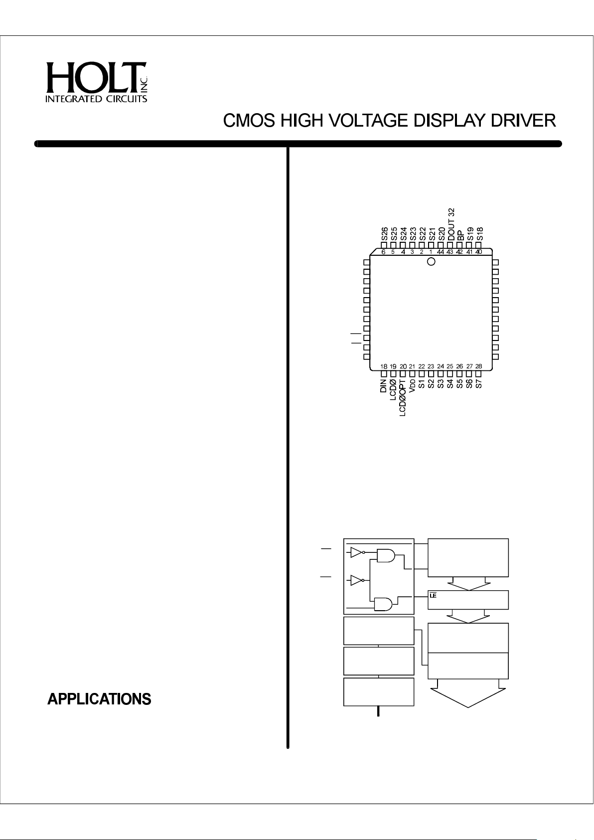
PINCONFIGURATION (TopView)
FUNCTIONALBLOCKDIAGRAM
Þ BP
Oscillator
Divider
Voltage
Translator
HighVoltage
Buffer
38Stage
ShiftRegister
38BitLatch
Voltage
Translators
HighVoltage
Drivers
SEGMENTS
DATAIN
CLK
Þ
Þ
Þ
DOUT38
DOUT32
DOUT30
GENERALDESCRIPTION
DIN Þ
CL Þ
CS Þ
LD Þ
LCDØ Þ
LCDØOPT Þ
(Seepage3-6foradditionalpackagepinconfigurations)
FEATURES
January2001
HOLTINTEGRATEDCIRCUITS
3-901/01(DS8020Rev.B)
39
38
37
36
35
34
33
32
31
30
29
S17
S16
S15
S14
S13
S12
S11
S9
S8
V
S10
EE
S27
S28
S29
S30
S31
S32
N/C
V
LD
SS
CS
CL
7
8
9
10
11
12
13
14
15
16
17
HI-8020J-85
&
HI-8120J-85
44-PIN
PLASTIC
PLCC
FUNCTIONALDESCRIPTION
WheneveraLogic"0"isappliedtotheChipSelect()
input,onebitofdataisclockedintotheshiftregisterfromthe
serialdatainput(DIN)witheachnegativetransitionofthe
Clock()input.isinternallytiedtoVSSonsome
versions.ALogic"1"presentattheLoad(LD)inputwill
causeaparalleltransferofdatafromtheshiftregistertothe
datalatch.IftheLoad(LD)inputisheldhighwhiledatais
clockedintotheshiftregister,thelatchwillbetransparent.
AllfourlogicinputsareTTLcompatibleontheHI-8020and
CMOScompatibleontheHI-8120.
Todisplaysegments,aLogic"1"isstor edintheappropriate
shiftregisterbitposition,andthesegmentoutputisout-ofphasewiththebackplane.
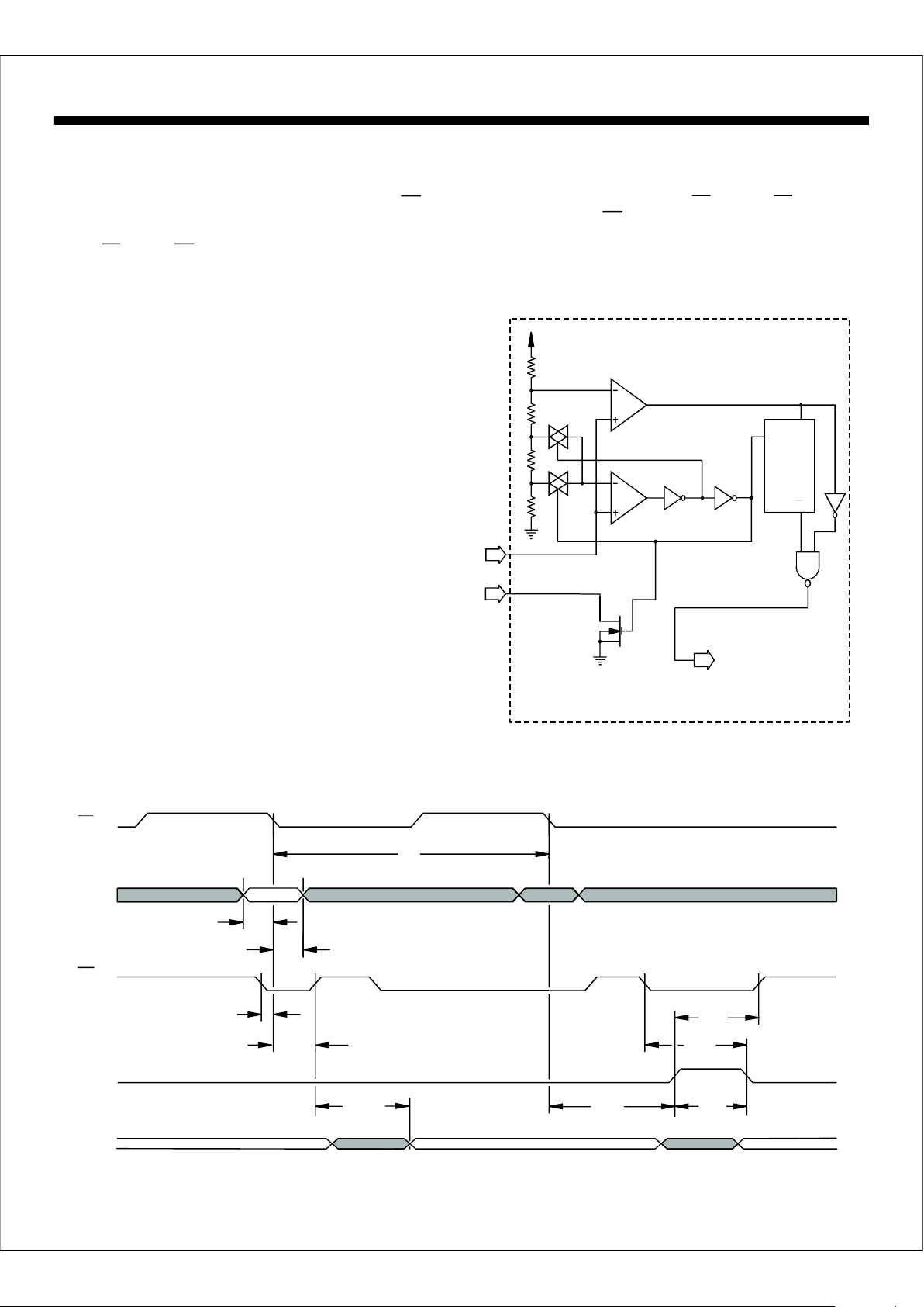
Thebackplaneoutputfunctionsin1of2modes;externally
drivenorself-oscillating.WhentheLCDØinputisexternally
drivenwiththeLCDØOPTinputopencircuit(Figure2),the
backplaneoutputwillbein-phasewithLCDØ.Utilizingthe
self-oscillatingmode,inputsLCDØandLCDØOPTaretied
togetherandconnectedtoanRCcircuit(Figure3).
A150Kresistorwitha470pFcapacitorgeneratesan
approximatebackplanefrequencyof100Hz.The
LCDØ/LCDØOPToscillatorfrequencyi sdividedby256to
determinethebackplaneoutputfrequency.Theresistor
value(R)mustbeatleast30Kforproperself-oscillator
operation.
Fordisplayshavinganumberofsegmentsgreaterthan38,
twoormoreofthedisplaydriversmaybecascadedtogether
byconnectingtheserialdataoutput(DOUT)fromthefirst
driver,totheserialdatainput(DIN)ofthefollowingdriver,
etc.(SeeFigures2&3).Dataout(DOUT)willchangestate
CS
CLCS
W
W
HI-8020/HI-8120Series
TIMINGDIAGRAM
t
CSH
t
CSS
t
DS
t
DH
t
CL
t
CDO
t
LS
t
LW
t
CSL
t
LCS
CL
INPUT
DIN
INPUT
CS
INPUT
LD
INPUT
DOUT
OUTPUT
VALID
VALID
HOLTINTEGRATEDCIRCUITS
3-10
INTERNALOSCILLATORCIRCUIT
TOBACKPLANE
TRANSLATOR
ANDDRIVER
÷256
C
R
LCDØ
OPT
LCDØ
Figure1.
Q
VALID
ontherisingedgeoftheClock().Clock(),Load(LD)
andChipSelect()shouldbetiedincommonwitheach
other,respectively,betweenallcascadeddisplaydrivers.
CLCL
CS

HI-8020/HI-8120Series
NOTE:Stressesabovethoselistedunder"AbsoluteMaximumRatings"maycausepermanentdamagetothedevice.Thesea restressratingsonly.
Functionaloperationofthedeviceattheseoranyotherconditionsabovethoseindicatedintheoperationalsection softhespecificationsisnotimplied.
Exposuretoabsolutemaximumratingconditionsforextendedperiodsmayaffectdevicereliability.
VoltagesreferencedtoVSS=0V
VDD........................
VEE................
SupplyVoltage
VDD-35Vto0V
0Vto7V
Voltageatanyinput,exceptLCDØ..-0.3toVDD+0.3V
VoltageatLCDØinput...............VDD-35toVDD+0.3V
DCCurrentanyinputpin...................................10mA
PowerDissipation......................................................300mW
OperatingTemperatureRange-Hi-Temp/Mil..-55°to+125°C
StorageTemperatureRange...........................-65°to+150°C
OperatingTemperatureRange-Industrial........-40°to+85°C
HOLTINTEGRATEDCIRCUITS
3-11
DCELECTRICALCHARACTERISTICS
VDD=5V,VEE=-25V,VSS=0V,TA=OperatingTemperatureRange(unlessotherwisespecified).
PARAMETERSYMBOLCONDITIONMINTYPMAXUNITS
OperatingVoltageVDD3.07.0V
SupplyCurrentIDDStatic,NoLoad200µA
IEEStatic,NoLoadf=100Hz150µA
InputLowVoltage,HI-8020(exceptLCDØ)VIL00.8V
InputHighVoltage,HI-8020(exceptLCDØ)VIH2VDDV
InputLowVoltage,HI-8120(exceptLCD)VIL00.3VDDV
InputHighVoltage,HI-8120(exceptLCD
InputLowVoltage(LCDØ)VILXVEE3V
InputHighVoltage(LCDØ)VIHX3.5VDDV
InputCurrentIINVIN=0to5V1µA
InputCapacitance(nottested)CI5pF
SegmentOutputImpedanceRSEGIL=10µA10,000
BackplaneOutputImpedanceRBPIL=10µA450
DataOutCurrent:IDOHSourceCurrent,VOH=4.5V-0.6mA
I DOLSinkCurrent,VOL=0.5V0.6mA
BP
TTL
TTL
CMOS
W
W
Ø
Ø)VIH0.7VDDVDDVCMOS
PARAMETERSYMBOLVDDMINTYPMAXUNITS
CLClockPeriodt5V1200ns
ClockPulseWidtht5V520ns
DataIn-Setupt5V50ns
DataIn-Holdt5V400ns
ChipSelect-SetuptoClockt5V200ns
ChipSelect-HoldtoClockt5V450ns
Load-SetuptoClockt5V500ns
ChipSelect-SetuptoLoadt5V300ns
LoadPulseWidtht5V500ns
ChipSelect-HoldtoLoadt5V300ns
CW
DS
DH
CSS
CSH
LS
CSL
LW
LCS
DataOutValid,fromClockt5V800nsCDO
ACELECTRICALCHARACTERISTICS
VDD=5V,VEE=-25V,VSS=0V,TA=OperatingTemperatureRange(unlessotherwisespecified).

CASCADING-EXT.OSCILLATOR
HI-8020/HI-8120Series
CASCADING-RCOSCILLATOR
DIN
HI-8020J-85
CS
LCDØ
CL
LD
DOUT
BP
SEGMENTS
1-33
DIN
HI-8020J-85
CS
LCDØ
CL
LD
DOUT
BP
SEGMENTS
33-64
DIN
HI-8020J-85
CS
LCDØ
CL
LD
DOUT
BP
SEGMENTS
65-96
BACK
PLANE
LD
CL
CS
DIN
HI-8120J-85
CS
LCDØ
CL
LD
DOUT
BP
SEGMENTS
1-32
LCDØOPT
DIN
HI-8120J-85
CS
LCDØ
CL
LD
DOUT
BP
SEGMENTS
33-64
LCDØOPT
DIN
HI-8120J-85
CS
LCDØ
CL
LD
DOUT
BP
SEGMENTS
65-96
LCDØOPT
BACK
PLANE
470pf
150K W
LD
CL
CS
Figure2
Figure3
HOLTINTEGRATEDCIRCUITS
3-12
ADDITIONALHI-8020/HI-8120PINCONFIGURATIONS
(Seepage3-9for44-PinPlasticPLCC)
S5
S4
S3
S2
S1
S38
S37
V
LCDØ
DIN
LD
DD
CL
S17
S18
S19
BP
DOUT38
S20
S21
S22
S23
S24
S25
S26
7
8
9
10
11
12
13
14
15
16
17
18
42
41
40
39
38
37
36
35
34
33
32
HI-8020S-61
HI-8120S-61
HI-8020SM-62
&
HI-8120SM-62
48-PIN
CERAMIC
LCC
S5
S4
S3
S2
S1
S38
S37
V
DIN
LD
DD
LCDØ/LCDØOPT
CL
S17
S18
S19
BP
DOUT38
S20
S21
S22
S23
S24
S25
S26
7
8
9
10
11
12
13
14
15
16
17
18
42
41
40
39
38
37
36
35
34
33
32
HI-8020S-63
HI-8120S-63
HI-8020SM-64
&
HI-8120SM-64
48-PIN
CERAMIC
LCC
PINDESCRIPTIONS
SYMBOLFUNCTIONDESCRIPTION
VSSPOWER0Volts
INPUTLogicinputChipselect
INPUTLogicinputClocksshiftregisteronnegativeedgeandDOUTpinsonpositiveedge
LDINPUTLogicinputSegmentoutputsequalshiftregisterdataifLoadishigh
DININPUTLogicinputShiftregisterdatainput
LCD0INPUTAnaloginputDisplayclockinputandisalwaysbondedout.CanswingfromVEEtoVDD
LCD0OPTOUTPUTAnalogoutputBondedoutonlyifanRCoscillatorisrequired
VDDPOWER5Volts
VEEPOWEROVoltsto-30Volts
DOUTOUTPUTLogicoutputSelectedpinoutcanprovideshiftregistertapsatpositions30,32,34,or38
BPOUTPUTDisplaydr iveoutputLowresistancedriveforthebackplaneandswingsfromVDDtoVEE
SegmentsOUTPUTDisplaydriveoutputHighresistancedriveforeachsegmentandswingsfromVDDtoVEE
CS
CL

HI-8020/HI-8120Series
ORDERINGINFORMATION
SEMI-CUSTOMPACKAGING
HOLTINTEGRATEDCIRCUITS
3-13
TheabovepartnumbersrepresentsomeofthetypicalconfigurationsoftheHI-8020&HI-8120products.Theycanalsob eprovided
withavariednumberofoutputsegments(30,32and38),witheitherindustrialormilitaryscreeningandinawidevari etyofpackages.
Listedbelowarecurrentlyavailablepackages.PleasecontacttheHoltSalesDepartmentforyourspecificrequirem ents.
PACKAGENO.
DESCRIPTIONLEADS
PLASTICDUAL-IN-LINE(PDIP)40
48
PLASTICQUADFLATPACK(PQFP)52
PLASTICJ-LEADCHIPCARRIER(PLCC)44
CERAMICDUAL-IN-LINE(CDIP)40
48
CERAMICLEADLESSCHIPCARRIER(LCC)40
48
CERAMICJ-LEADCHIPCARRIER44
48
CERAMICLEADEDCHIPCARRIER40
48
PART NUMBER OF MASTER PACKAGE TEMPERATURE BURN LEAD
NUMBER SEGMENTS /SLAVE DESCRIPTION RANGE FLOW IN FINISH
TTL Input Logic
HI-8020J-85 32 BOTH 44 PIN PLASTIC J LEAD -40°C TO +85°C I NO SOLDER
HI-8020S-61 38 MASTER 48 PIN CERAMIC LEADLESS CHIP CARRIER -40°C TO +85°C I NO GOLD
HI-8020SM-62 38 MASTER 48 PIN CERAMIC LEADLESS CHIP CARRIER -55°C TO +125°C M YES SOLDER
HI-8020S-63 38 SLAVE 48 PIN CERAMIC LEADLESS CHIP CARRIER -40°C TO +85°C I NO GOLD
HI-8020SM-64 38 SLAVE 48 PIN CERAMIC LEADLESS CHIP CARRIER -55°C TO +125°C M YES SOLDER
CMOS Input Logic
HI-8120J-85 32 BOTH 44 PIN PLASTIC J LEAD -40°C TO +85°C I NO SOLDER
HI-8120S-61 38 MASTER 48 PIN CERAMIC LEADLESS CHIP CARRIER -40°C TO +85°C I NO GOLD
HI-8120SM-62 38 MASTER 48 PIN CERAMIC LEADLESS CHIP CARRIER -55°C TO +125°C M YES SOLDER
HI-8120S-63 38 SLAVE 48 PIN CERAMIC LEADLESS CHIP CARRIER -40°C TO +85°C I NO GOLD
HI-8120SM-64 38 SLAVE 48 PIN CERAMIC LEADLESS CHIP CARRIER -55°C TO +125°C M YES SOLDER

PackageType:
PINNO.1IDENT
.045x45°
.050 ± .005
(1.27 ± .127)
.045x45°
PINNO.1
44-PINPLASTICPLCC
SEEDETAIL
A
.172 ± .008
(4.369 ± .203)
DETAILA
.020MIN
(.508 ΜΙΝ )
.025
.045
R
.690 ± .005
(17.526 ± .127)
SQ.
.610 ± .020
(15.494 ± .508)
.031 ± .005
(.787 ± .127)
.653 ± .004
(16.586 ± .102)
SQ.
.017 ± .004
(.432 ± .102)
.015±.002
(.381 ± .051)
.009
.011
44J
HI-8020/HI-8120PACKAGEDIMENSIONS
inches(millimeters)
HOLTINTEGRATEDCIRCUITS
1
PackageType:
PIN1IDENT.
PIN1IDENT.
.040TYP.
(1.016TYP.)
.020TYP.
(.508TYP.)
.090MAX.
(2.286MAX.)
.563 ± .009
(14.300 ± .228)
SQ.
.040 ± .007
(1.016 ± .178)
48-PINCERAMICLEADLESSCHIPCARRIER
48S
 Loading...