


AN-62003 Rev. A Holt Integrated Circuits
ADK-620x3 User’s Guide:
Evaluation Board for
HI-62003 BC/RT/MT &
HI-62023 RT only Devices
December 2018
Holt Integrated Circuits 2
REVISION HISTORY
Revision
Date
Description of Change
AN-62003, Rev. New
12-02-18
Initial Release
AN-62003, Rev. A
12-12-18
Update Kit Contents
Holt Integrated Circuits 3
Introduction
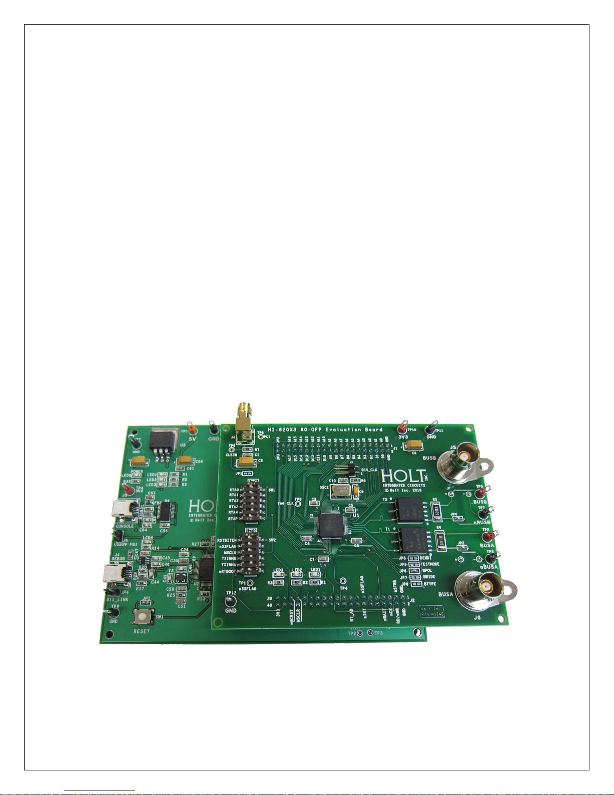
The Holt H-620x3 Evaluation board demonstrates the broad feature set of Holt’s MIL-STD-1553 HI-620x3
family, consisting of:
HI-62023 Remote Terminal device
HI-62003 Remote Terminal, Bus Controller and Monitor device
The H-620x3 family is a set of MIL-STD-1553B bus communication devices containing protocol
management and physical bus interface circuitry. The 2-board assembly and C project reference design
provides a ready-to-run evaluation platform demonstrating operation of Bus Controller, Bus Monitor
and Remote Terminal. For convenience, this kit includes IAR Systems Embedded Workbench® for ARM,
and a fully integrated debug interface for the ARM Cortex M3 microcontroller. Note that in this ADK620x3 guide, the HI-62003 is used as the reference device because it contains all available features; the
HI-62023 is an RT-only device, so the BC and MT functions in the menu are not applicable in this case.
This guide describes how to set up and run the board. Additional support material and all required
project software are found in the included Holt USB drive. A version of the demonstration software is
already programmed into the microcontroller flash; the board is operational right out of the box without
installing or running the provided software development tools.
Figure 1 HI-620x3 Evaluation Board, mounted on the ARM Cortex MCU Board.
Holt Integrated Circuits 4
Evaluation Kit Contents
This User Guide.
Holt HI-620x3TM Project Software and Documentation on USB drive.
Installation for IAR Systems Embedded Workbench® for ARM (32KB KickStart.), on USB drive.
2x USB interface cables.
2-board assembly comprised of:
Upper DUT board with 620x3
TM
device and dual transformer-coupled MIL-STD-1553 bus interfaces.
Numerous DIP switches configure board operation.
Lower MCU board with ARM Cortex M3 16-/32-bit microprocessor, debug interface and regulated
3.3VDC power supply.
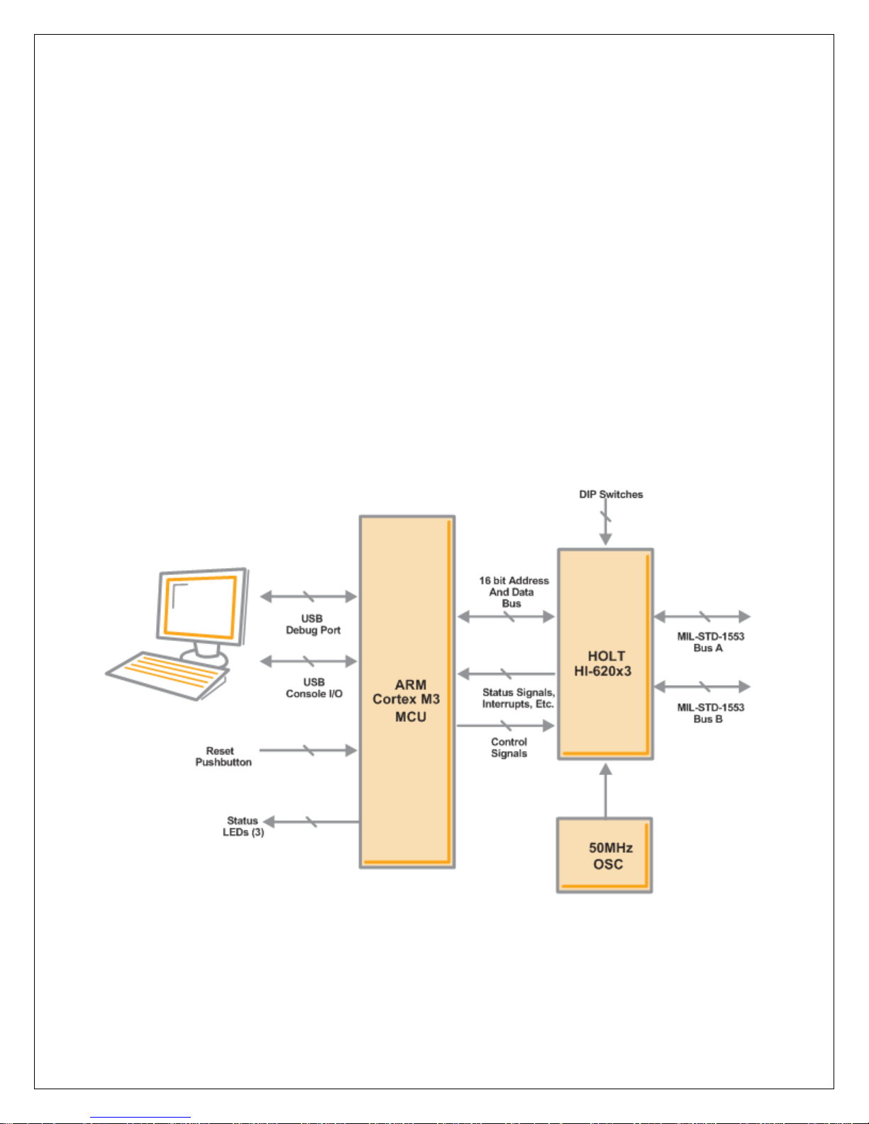
Hardware Block Diagram
Holt Integrated Circuits 5
Default Switch Settings (620x3 board)
RT ADDRESS (SW1)
SWITCH
POSITION
DESCRIPTION
SW1, 5-1
00011
(ON = 0)
Sets the RT address, default is set to 03
SW1, 6
OFF
OFF = RT address parity bit ‘1’, must be odd parity or
device will not work
CONFIG 1 (SW2)
SWITCH
DEFAULT
DESCRIPTION
SW2, 1
OFF
RSTBITEN: OFF , internal self test enabled on reset
ON – Internal self test disabled
SW2, 2
OFF
nSSFLAG/EXT_TRIG: ON, 1553 SSFLAG bit is not set
OFF, SSFLAG bit is set
Note: If External trigger is used SW2,2 should be OFF
SW2, 3
OFF
MSCLR: ON , Hardware reset
SW2, 4
ON
TXINHA: OFF, inhibits transmission on BUSA
SW2, 5
ON
TXINHB: OFF, inhibits transmission on BUSB
SW2, 6
OFF
nRTB: ON, nRTBOOT pin = 0, 1760 mode
OFF, nRTBOOT= 1 (open)

Holt Integrated Circuits 6
Default Jumper Settings
HI-620x3 Board
JUMPER
POSITION
DESCRIPTION
JP1
OFF
Link to send clock to ARM board (not normally used).
JP2
ON
Ground BUSA negative line.
JP3
ON
Grounds TEST pin (disables test mode)
JP4
ON
Ground BUSB negative line.
JP5
OFF
BENDI: ON, Little Endian Data
OFF, Big Endian Data
JP6
ON
WPOL: ON, WAIT pin is active low
OFF, WAIT pin is active high
JP7
OFF
BWIDE: ON, Bus width is set to 8 bits
OFF, , Bus width is set to 16 bits
JP8
OFF
BTYPE: ON, Motorola type data bus
OFF, Intel type data bus
JP9
ON
BUSB LOAD: ON, 70Ω Load connected
OFF, 70Ω Load disconnected
JP10
ON
BUSA LOAD: ON, 70Ω Load connected
OFF, 70Ω Load disconnected
JP11, JP13
ON
Transformer 1:2.5 ratio selected
JP12, JP14
OFF
Transformer unused option
J7
OFF
Connect to disable on board oscillator (use when an
external clock is connected to J4)
Holt Integrated Circuits 7
Test Points
TEST POINT
DESCRIPTION
TP1
nSSFLAG output or input for external trigger
TP2
Positive connection for 1553 Bus A
TP3
Negative connection for 1553 Bus A
TP4
nINCMD, a ‘0’ indicates 620x3 activity (default)
nMCRST, mode code 8 reset output (when enabled)
TP5
Positive connection for 1553 Bus B
TP6
HI-620x3 input clock
TP7
Negative connection for 1553 Bus B
TP8
Monitor HI-620x3 input clock
TP9
Input for TAG clock
TP10
3.3V supply for HI-620x3 (supplied from ARM board)
TP11/12
Ground connection
ARM Board
Jumpers
JUMPER
POSITION
DESCRIPTION
JP1
OFF
Link for Mode Code 8 to reset board.
JP2
ON
Link for using NonZero Wait type interface Used.
JP3
OFF
Link for using Zero Wait type interface.
JP4
OFF
Not Used.
J1
OFF
Link for external ARM clock.
J6
OFF
Link to enable supply from USB 5V, make sure this is
disconnected if using bench supply
Holt Integrated Circuits 8
LEDs
LED #
DESCRIPTION
LED1
Software defined LED.
LED2
Software defined LED.
LED3
Software defined LED.
Hardware Design Overview
Refer to the end of this guide for separate schematic diagrams and bills of material for the upper
DUT board and lower MCU board.
The detachable DUT board can be separated from the provided MCU board for connection to a
user-supplied alternate microprocessor or FPGA board. The inter-board headers are located on
0.1” (2.54 mm) grid for compatibility with generic prototyping boards. All host interface signals
go through the inter-board headers. Several configuration pins including the Remote Terminal
address setting pins are controlled by two DIP switches on the upper DUT board; these signals
are not available on the inter-board headers.
The lower ARM Cortex M3 board is based on the flash-programmable Atmel AT91SAM3U-EK
microprocessor. A 16 bit data/address bus from the ARM connects to the DUT. A USB serial port
provides console I/O (optional). A RESET pushbutton resets the ARM microprocessor, which in
turn controls the DUT Master Reset signal.
The ARM Cortex M3 board includes “J-Link On Board” debug interface, licensed from
www.segger.com, providing out-of-box readiness without having to buy a costly JTAG debug
cable. The kit includes a simple USB cable for connecting the board’s debug interface to your
computer.

Holt Integrated Circuits 9
620x3 Host Interface
HI-620x3 features a 16 bit parallel data bus and has 64K x 16 word SRAM address space. It is offered in
an 80 pin QFP or QFN package.
The 620x3 has data transfer speeds that depend on which of the four available clock frequencies is
selected. The board is supplied with a 50MHz XTAL oscillator module, so by default the software will set
up 50MHz operation. However an external clock can be input through SMA connector J4, if this is done
jumper J7 should be connected. The device will run on a 50, 40, 20 or 16MHz clock, but the appropriate
register setting must be sent to register 0x18.
Control Switches
SW2 has six control functions that affect operation of the HI-620x3, these are explained in the
configuration section, please check they are in the default position before continuing.
RT address set up
The RT terminal address is set using DIP switches, before applying power. RT addresses 3 and 4
are utilized by the preprogrammed Bus Controller message repertoire. The 6-position DIP switch
SW1 should already be set with the address value 03, plus odd parity.
1760 Mode (all devices)
In this mode, the RT device responds with the Status Word’s Busy bit set within 2ms of Master
Reset pin rising edge. To test this feature, the device can be powered up without the software
running (for example by using SW1 RESET switch to hold the MCU in reset). If the MSCLR switch
is toggled on the ADK (SW2/3) the device can quickly respond to a BC command with the ‘Busy’
bit set.
1553 Bus Interface
Note 1: Connecting Bus Negative to ground is strictly a bench test convenience feature. Most
performance characteristics of transmitted and received 1553 signals are specified using
differential line-to-line measurements at the bus stub, Bus Positive minus Bus Negative. This
corresponds to the red and black “BUS” test points adjacent to the transformers on the right
side of the upper circuit board. While two oscilloscope probes connected to red and black may
be used in conjunction with scope’s Ch1-Ch2 math function, a single probe connected to Bus
Positive provides the same signal display when Bus Negative is grounded. This frees up scope
probes for other purposes. The nINCMD (TP4) signal can be used to trigger the scope as shown
in magenta trace on plots from the next page, this signal goes low during 1553 activity.
Do not include a provision for grounding Bus Negative in your production design.
Note 2: For stand-alone testing (without connection to a conventional MIL-STD 1553 bus) the hardware
provides on-board 70Ω termination resistors. This is strictly a bench test convenience feature
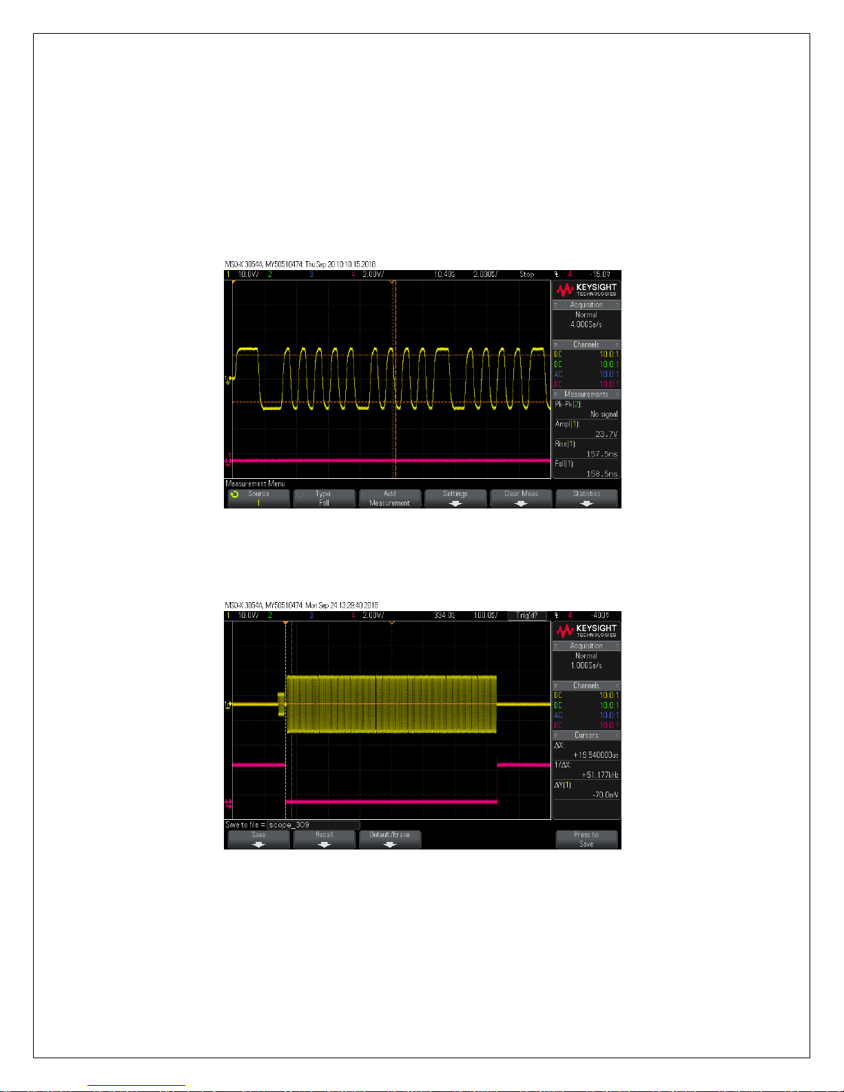
Holt Integrated Circuits 10
that supports demonstration of BC and RT without external 1553 bus connections. When using
the RT/MT mode the RT can fully transact messages, with or without the bus monitor.
On-board termination resistors are not used when connecting to a properly terminated MIL-
STD-1553 bus. Do not include a provision for termination resistors in your production design.
BusA 1553 output and nINCMD signal, in BC mode generating bus command
BusA 1553 output and nINCMD signal, in RT mode, responding to TxData command

Holt Integrated Circuits 11
Initial Setting Up
The Holt 620x3 Application Development Kit is designed to support the HI-62003 and HI-62023
devices in the QFP 80 pin package. The HI-62003 is used as the example, this has 64K of 16 bit
SRAM and will operate in all three modes; Remote Terminal (RT), Bus Controller (BC), SMT Bus
Monitor (MT). The HI-62023 can also be fitted, this has RT only capability.
Windows 7, 10 …
Install the free open-source terminal emulation program, TeraTerm 4.71, by running the
provided teraterm-4.71.exe installer program from the Holt CD. Accept the license agreement
stating redistribution is permitted provided that copyright notice is retained. The notice can be
displayed from the TeraTerm window by clicking Help then clicking About TeraTerm. Continuing
to install…
Accept the default install destination and click Next.
At the Select Components screen, unselect all options except Additional Plugin =
TTXResizeMenu and click Next.
Select the installed language, then click Next.
Accept the default Start Menu folder, then click Next.
Select any desired shortcuts, then click Next.
At the Ready to Install screen, click Install.
Run the TeraTerm program. At the New Connection screen, select (x)Serial and choose the
selected COM port. Click Setup then Serial Port to open the serial port setup window. Choose
these settings: Baud Rate: 115200, Data: 8 bits, Parity: none, Stop: 1 bit, Flow Control: none.
The board can be powered from both a 5VDC bench power supply or the 5V USB supply, if using
the USB supply jumper J6 on the lower ARM board should be closed, note however that on
many PCs the USB does not have sufficient power to supply the board when it is transmitting. If
using the bench supply make sure J6 is open. If TeraTerm is running and configured correctly,
the command menu below should appear in the console window. This menu appears whenever
board power is applied, or the RESET pushbutton is pressed. After verifying correct TeraTerm
communication with the evaluation board, the terminal set up can be saved by clicking Setup
then Save Setup.

Holt Integrated Circuits 12
The RT terminal address is set using DIP switches SW1. RT address 3 is utilized by the preprogrammed
Bus Controller message repertoire. The 6-position DIP switch should already be set with the address
value 03, plus odd parity.
The dates and times shown will differ from the screen captures shown below.
Press ‘w’ to reset the HI-620x3, then press ‘d’ to display the HI-620x3 registers, display should look
similar to below:

Holt Integrated Circuits 13
Reg #5 data is the time tag counter and will continually change, Reg #9 is the RT address register and
content 0007 reflects RT address 3 is set. Reg #1C is the self test register and a800 reflects that the
protocol test was run on power up and passed. Note the RSBITEN pin has to be high for this test to run
on reset.
General Structure of Demo Functions
The Holt API demonstration program is run from the source files in the src (source) folder. The main.c
file calls the console.c and executes demo functions in bcdemo.c, bcAsyncDemo.c and rtmtdemo.c. The
Holt API runtime library is contained in the library HI-62xxx lib as executable object code. Files xdemo.c
contain the demo initialization API function calls supporting demonstrations executed from the console
menu to initialize the BC, RT and monitor terminals. Key presses are detected in console.c
Commands ‘a’ and ‘b’ transmit BC async commands onto the A and B bus respectively and can be
viewed on an oscilloscope. The ‘f’ command will transmit a Major/Minor frame. These demos
demonstrate how Holt API’s are used to generate BC Asynchronous messages, Major/Minor frames, low
Holt Integrated Circuits 14
priority and high priority messages. View these messages with external MIL-STD-1553 test equipment or
on an oscilloscope.
This exercise uses the internal BC to transmit messages, so message traffic data is displayed on the
console. If an external BC is already connected to the bus jack though a bus coupler, it is okay to leave it
connected, but disable any external BC transmissions that will conflict with the on-chip BC
transmissions. A snap shot of the output data is shown below:
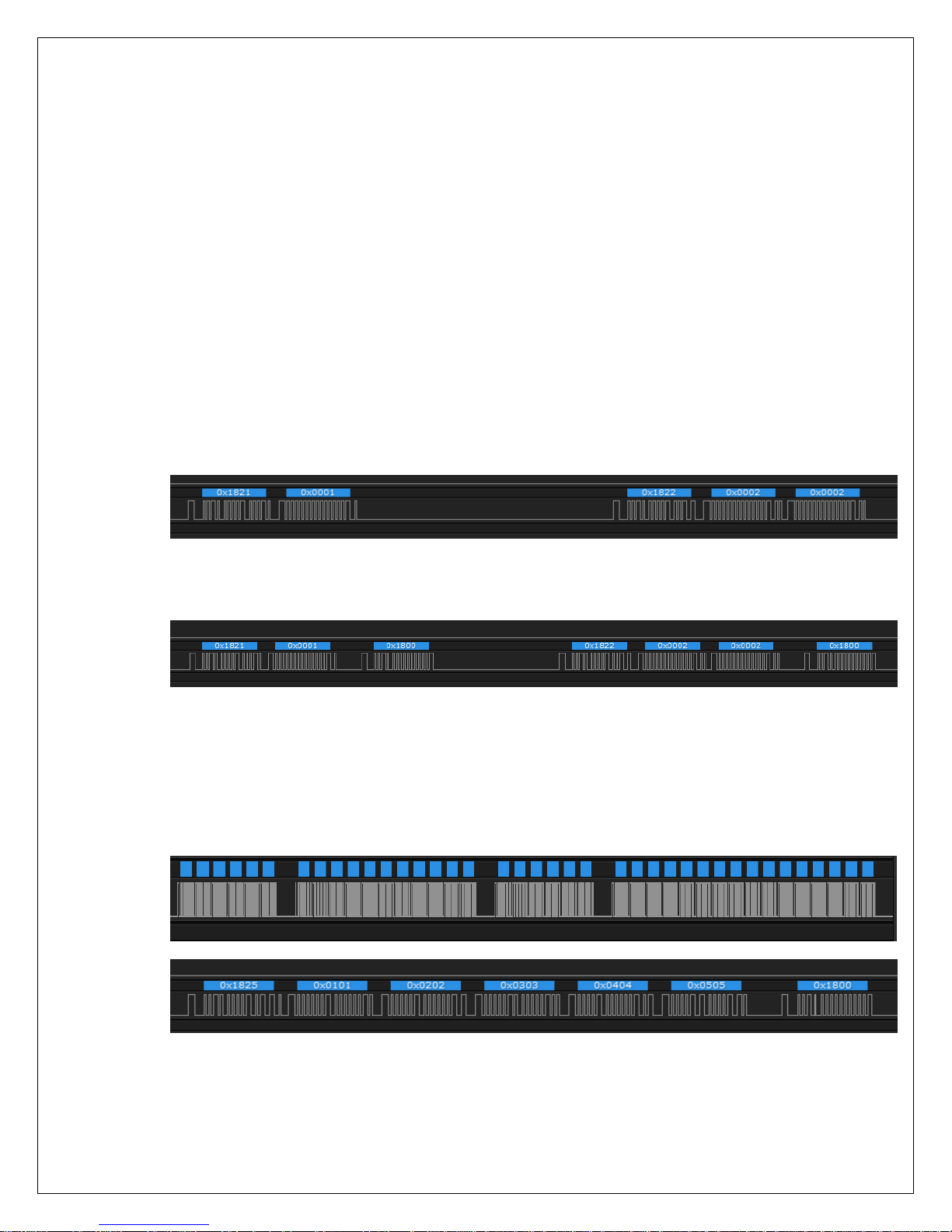
BC Mode (using an external RT)
1. Commands ‘a’ and ‘b’ transmit BC async commands onto the A and B bus respectively and can
be viewed on an oscilloscope, as shown below. These are Receive data commands to an RT
address = ‘3’. A series of four RxData commands are sent with 1 to 4 data words.
2. Connect an RT to BUSA and set RT address to 3, monitor the Bus with a oscilloscope or monitor,
a a response similar to below should be seen, with the RT responding with a clear status word:
3. The ‘f’ command will transmit a Major/Minor frame. These demos demonstrate how Holt API’s
are used to generate BC Asynchronous messages, Major/Minor frames, low priority and high
priority messages. Below is a snap shot of the major frame sequence containing 4 minor frames,
this is continually repeated, the second snap shot shows the first minor frame:
The 0x1800 word is the RT address 3 responding with a clear status.

Holt Integrated Circuits 15
4. The message data for the Major/Minor frames is contained in the bcdemo.c program and can
easily edited. As shipped RT address 3 is used.
RT Mode, using an external BC
Use an external BC tester (such as Ballard USB 1553) to transmit messages to the demo
board.
1. When an external BC is connected using conventional 1553 buses, use cables to connect the
demo board circular tri-axial bus jacks to bus coupler ports on the A and B bus networks. In this
case, the on-board dummy bus load 70Ω resistors should be disconnected. If bus couplers are
not readily available, bench testing can be done by enabling the on-board dummy bus load 70 Ω
resistors (R4, 5) and connecting BC tester cables directly to the demo board tri-axial jacks for
buses A and B.
2. Press ‘w’ command to reset device, then ‘r’ to set RT mode. This configures the HI-620x3 into an
RT terminal, with the address set on DIP switch SW1. The screen below will be displayed.
3. RT is set to single buffered mode. This RT set up supports data write and read from RT Sub-
address 1 and most mode codes, please refer to Holts API software manual for more details.

Holt Integrated Circuits 16
4. As in example before, use 1553 tester to a 03-T-01-02 Xmt command (0x1822). The Bus data
should look similar to below.
Response to receive two data words to SA1
Response to Transmit two words from SA1

Holt Integrated Circuits 17
RT/MT Mode, using an external BC
Use an external BC tester (such as Ballard USB 1553) to transmit messages to the demo
board.
1. Press ‘w’ command to reset device, then ‘c’ to set RT/MT mode. This configures the device into
an RT terminal and a Monitor. The screen below will be displayed:
2. RT is set to single buffered mode. The RT is set up as in RT mode above, but additionally it will
monitor traffic on the bus and report the data log to the terminal screen. Send a 03-T-01-02
command from the 1553 tester, then send a 03-R-01-02 command. The screen will show a data
log similar to below:

Holt Integrated Circuits 18
1st line shows the MSG#, the time stamp, BUS being used, type of message
2nd line shows the command hex code and the subtext abbreviation for the command
3rd line shows the data content of the command in the format:
RT ADD - Tx/Rx Type –Subaddress - Word length
3. Send a Mode code 18 (Transmit last command), the command 03-R-01-02 sent above should be
logged as below, note only the hex content (0x1C22) of the message is displayed:
MT Mode, using an external BC
Use an external BC tester (such as Ballard USB 1553) to transmit messages to the demo
board.
1. The monitor mode is very similar to RT/MT mode but the RT is not enabled, the monitor
functions the same as in RT/MT section above.
2. Press ‘w’ command to reset device, then ‘t’ to set MT mode. This configures the device into a
Monitor only. The screen below will be displayed, additionally if a 03-T-01-02 command is sent a
log and response will be shown, with no response this time as the RT is disabled:

Holt Integrated Circuits 19

Holt Integrated Circuits 20
Getting Started with the Holt API demo software project and installing
IAR Systems Embedded Workbench for ARM Compiler
Getting Started with the Holt API demo software project and installing IAR Systems Embedded
Workbench for ARM Compiler
Installed IAR Systems Embedded Workbench for ARM (EWARM ) compiler is required BEFORE
adding the Holt demo projects so all Atmel board library files and the demo project folder are
created in the proper location. Follow the “Holt HI-620x3 API Demo Project Installation Guide”
found in the Project folder on the Holt USB DRIVE. Before proceeding to the next steps IAR must
be installed and the two Holt project folders must be in the proper folder locations, according to
that guide. Instructions beyond this point assume you have completed the above installation
tasks.
Launch IAR Embedded Workbench from the Windows Start menu. A blank screen should appear.
Open the Holt HI-620x3 API Demo Project from the IAR File pull-down menu, click on
File/Open/Workspace and navigate to the project folder location and select “HI-62xx.eww” and
click the Open button.
An IAR Workspace window should appear on the left side as shown below. If the Workspace
directory pane is missing, select “Workspace” from the View pull-down menu. Make any
window adjustments or open any of the folder groups to view included files to suit your
preferences.
Double click the main.c file, it should appear in the text editor pane, similar to the screen
capture below.
The first time a project is unzipped and installed in the appropriated folder a Rebuild All should
be performed (from Project pull down menu).
IAR getting started, project management and other guides are available from the IAR
Workbench Help pull down menu.

Holt Integrated Circuits 21
Mode Holt Project Configurations
IAR project configurations are used to re configure the demo software using preprocessor macros. Holt
uses a common code base for multiple projects. This means there are functions not used in this project
but are left in the C and H files. The IAR compiler uses the macros to decide which sections of code to
build and link. Some references to HI-6130 or HI-6131 are to be expected. In some cases, functions are
simply not used or macros are used inside a function to select appropriate code.

Holt Integrated Circuits 22
The API library source code is not provided in the standard ADK. The full API source code is available
with a signed Holt software license agreement (SLA). The standard ADK demos are fully functional
otherwise, and API projects can be built without the API C source code. Contact Holt sales for the SLA for
the optional API C source code.
The IAR embedded workspace provides may of the commonly used tasks as short-cut buttons on the top
as shown:
Application Development Kit Notes
620x3TM was designed for compatibility with microcontrollers having a 16 or 8 bit data bus interface. The
device is split into address space for RAM or register locations, and is selected using the nMEM/REG
control pin which is connected to address pin A17. The menu command ‘d’ will read all register
addresses from 0x00 to 0x01F.
When using the ARM debugger, the register address space starts at the ARM address 0x60000000 and
the RAM at 0x60020000.
The console I/O option using TeraTerm includes a menu option that reads and displays register content
including pending interrupt register status. Remember that Pending Interrupt bits automatically reset
after read occurs.
Stop
Debug
Toggle
Brkpoint
Restart
Make
Reset
Break
Step
Into
Run to
Cursor
Go
Step
Over
Compile
IMPORTANT EMBEDDED WORKBENCH BUTTONS

Holt Integrated Circuits 23
Project File List with Selected Descriptions
Most of the function names are self-explanatory, some functions retain the names from the
original HI-6131 or 6130 devices they were written for, don’t worry about this they work fine
with the HI-620x3 family.
Board_6200.c/h
Handles definitions for HI-620x3 ARM clock rate and interface settings.
board_lowlevel.c/h
Hardware configuration, such as ARM PLL settings .
613x_interrupts.c/h
Interrupt handling routines and configuration settings.
main.c
The primary program entry portal, main() demonstrates initialization sequence used to enabled
terminals. After initialization is complete, function calls demonstrate powerful addressing
methods for all RAM structures used by the enabled terminal modes. Demo initialization and
execution uses Holt high-level API in this demo kit.
ConfigureGpio(); initializes ARM MCU general purpose I/O
console.c
Console functions used by all terminal modes:
ConfigureUsart1();
Show_menu();
chk_key_input();
list_all_regs();
Console functions used by Bus Controller (BC) mode:
bcAsync();
MajorMinorframe();
Console functions used by Remote Terminal: rtpoll();
Console functions used by Monitor MT: mtpoll.c
Console functions used by Monitor/Remote Terminal MT/RT:
rtmtdemo.c;
Console functions used by MT bus monitor modes:

Holt Integrated Circuits 24
Primitive console functions that "printf" redundant char strings to reduce program size:
print_null(), print_sp1sp(),print_b1sp(), print_b0sp();
print_dddn(), print_dd0n(), print_dd1n();
print_menuprompt(), print_line();
DisplayDecodedMsg(); used to display 1553 formatted data to the console when the ‘t’ monitor
command is used.
displayRTTraffic(); called from main; calls DisplayDecodedMsg()
Flash.icf - Project Linker File.
Holt API Library files
_HI-62xxx 1_0 LIB.a – Precompiled Holt API library.
This file, with extension .a, is the precompiled Holt API library file, note: file name could have
a later revision number.
The standard API kit does not include the Holt API source files although the API header files are
included and grouped in the workspace Holt_API/src sub-folder.

5
5
4
4
3
3
2
2
1
1
D D
C C
B B
A A
RTA pins have
pull 200uA ups.
TAG
CLK
nSSFLAG/EXTTRG
FOR ALL DIP SWITCHES
UP = LOGIC-1
REMOTE
TERMINAL
ADDRESS
INCMD
(message
being processed)
1
3
2
1
3
2
***DNI***
3V3
***DNI***
***DNI***
***DNI***
***DNI***
1:2.5 ratio
1:2.5 ratio
D0
D1
D2
D3
D4
D5
D6
D7
D8
D9
D10
D11
D12
D13
D14
D15
D[0..15]
MSCLR
nRTBOOT
A2
A3
A4
A5
A6
A7
A8
A9
A10
A11
A12
A13
A1
A14
A15
A16
nRTBOOT
D[0..15]
GND GND
A0 D0
A1 D1
A2 D2
A3 D3
A4 D4
A5 D5
A6 D6
A7 D7
A8 D8
A9 D9
A10 D10
A11 D11
A12 D12
A13 D13
A14 D14
A15 D15
A16
GND GND
3V3
ABUS
nABUS
nBBUS
BBUS
D[0..15]
nSSFLAG
nWAIT
RD/nWR
TXINHB
RSTBITEN
TXINHA
TXINHB
nSSFLAG
A[0..16]
nSTRB
RSTBITEN
RT_AD_LAT
nINT
MSCLR
CLKIN
A17
A0
TXINHA
nCE
3V3
nMCRST
A[0..16] D[0..15]
A17
3V3 3V3
RD/nWR
nCE
nWAIT
nINT
RT_AD_LAT
nSTRB
3V3
MSCLR
nMCRST
CLKIN
3V3 3V3
CLKIN
3V3
nSSFLAG
Title
Size
Document Number Re v
Date: Sheet
of
HI-620x3 Carrier.DSN B
HI-620X3 80-QFP Evaluation Board
Custom
11Wednesday, November 28, 2018
Title
Size
Document Number Re v
Date: Sheet
of
HI-620x3 Carrier.DSN B
HI-620X3 80-QFP Evaluation Board
Custom
11Wednesday, November 28, 2018
Title
Size
Document Number Re v
Date: Sheet
of
HI-620x3 Carrier.DSN B
HI-620X3 80-QFP Evaluation Board
Custom
11Wednesday, November 28, 2018
J7
12
TP2
C10
.1uF
JP8
R4
70 1W
J6
BJ77
JP11
321 456
ON (CLOSED)
SW2
SMD 6-POS DIP Switch
LED3
JP13
T2
PM-DB2791S
4
5
6
7
8
1
2
3
J1
Header 2x20
1 2
3 4
5 6
7 8
9 10
11 12
13 14
15 16
17 18
19 20
21 22
23 24
25 26
27 28
29 30
31 32
33 34
35 36
37 38
39 40
JP7
TP3
JP4
321 456
ON (CLOSED)
SW1
SMD 6-POS DIP Switch
LED1
TP9
TP12
R2
270
TP6
C8
.1uF
OSC1
50.0MHz
OE
1
GD2OUT
3
VCC
4
C5
.1uF
JP3
TP8
TP10
TP11C7
.1uF
JP9
J2
Header 2x20
1 2
3 4
5 6
7 8
9 10
11 12
13 14
15 16
17 18
19 20
21 22
23 24
25 26
27 28
29 30
31 32
33 34
35 36
37 38
39 40
C3
.1uF
TP5
JP10
JP1
J5
BJ77
T1
PM-DB2791S
4
5
6
7
8
1
2
3
TP4
J4
SMA
1
2
JP2
+
C2
47uF
R3
270
JP14
C4
.1uF
LED2
R1
270
+
C9
4.7uF
JP6
TP1
R6
10K
HOLT
HI-62003
U1
HI-62XX3
A11
32
A10
80
TX_RX_A
68
nTX_RX_A
70
MEM_nREG
45
A08
29
BENDI
65
VCC_XCVRA
69
A07
28
A03
14
TX_RX_B
71
nTX_RX_B
73
A00
10
A02
12
TESTMODE
61
TAG_CLK
25
RTAD2
76
nMSTCLR
9
CLOCK_IN
13
A06
34
BWIDE
58
+3.3V_VCC_LOGIC
27
GND_LOGIC
1
nINCMD_nMCRST
56
A01
11
MSB/LSB
74
BTYPE
55
RT_AD_LAT
60
nSSFLAG_EXTTRIG
75
RTAD0
78
RTAD3
62
RTAD4
63
DB06
21
DB01
4
DB04
17
RTADP
79
RTAD1
77
DB00
3
DB02
5
DB03
6
DB05
18
GND_LOGIC
7
+3.3V_VCC_LOGIC
40
DB08
23
DB07
22
DB13
38
DB12
37
DB14
41
DB09
24
DB11
36
DB15
42
DB10
35
RSTBITEN
64
WAIT
53
nINT
54
TX_INH_A
67
nCE
52
TX_INH_B
66
nSTRBD
46
+3.3V_VCC_LOGIC
51
GND_LOGIC
19
nWE
57
WPOL
59
A15
44
A05
16
A09
30
A12
33
A13
49
A04
15
A14
43
VCC_XCVRB
72
+3.3V_VCC_LOGIC
2
+3.3V_VCC_LOGIC
8
+3.3V_VCC_LOGIC
20
nRTBOOT
31
GND_LOGIC26GND_LOGIC39GND_LOGIC48GND_LOGIC
50
RAM VDD
47
JP5
TP7
R750
+
C6
47uF
R5
70 1W
C1
.1uF
JP12

Holt Integrated Circuits, Inc.
PCB P/N: HV040
Bill of Materials
HI-620X3 80-QFP
Evaluation Board
Rev. B
November 29, 2018
Item Qty Description Reference Digikey P/N Mfg P/N
1 1
PCB, Bare, Evaluation Board N/A
NewTeck PCB# 14770
2 2
Capacitor, 47uF 20% 16V Tant SMD 6032 C2,C6
399-9739-1-ND
Kemet T491C476M016AT
3 1
Capacitor, 4.7uF 10% 16V Tant SMD 3216 C9
399-8439-1-ND Kemet T494A475K016AT
4 7
Capacitor, Cer 0.1uF 20% 50V Z5U 0805 C1,C3,C4,C5,C7,C8,C10
399-1176-1-ND Kemet C0805C104M5UACTU
5 2
Connector 3-Lug Concentric Triax Bayonet
Jack, Panel Front Mount TRB (BJ77)
J5,J6
MilesTek 10-06570
Trompeter Electronics BJ77
6 1
Connector SMA Jack R/A 50 Ohm PCB J4
A97593-ND
TE 5-1814400-1
7 2
Header, Male 2x20, .1" Pitch J1,J2 S2012EC-20-ND
Sullins PREC020DAAN-RC
8 1
Conn Header .100 Sgl RA 2 Pos Male J7
S1111E-02-ND Sullins PBC02SBAN
9
Conn solder jumper JP1-JP14
10 3
Led Green SMD 0805 LED1,LED2,LED3
160-1179-1-ND LiteOn LTST-C170GKT
11 1
Res 49.9, 1/8W 1% 0805 SMD R7
P49.9CCT-ND ERJ-6ENF49R9V
12 2 Res 69.8 Ohm 1W 1% 2512 SMD
R4,R5
RHM69.8BBCT-ND Rohm MCR100JZHF69R8
13 3
Res 270, 1/8W 5% 0805 SMD R1,R2,R3
P270ACT-ND Panasonic ERJ-6GEYJ271V
14 1
Res 10K 5% 1/8W 0805 R6
P10KACT-ND Panasonic ERJ-6GEYJ103V
15 2
Switch Tape Seal 6 Pos SMD SW1,SW2
CT2196MST-ND CTS 219-6MST
16 4
Test Point, White Insulator, 0.040" TP1,TP6,TP8,TP9 Optional
36-5002-ND Keystone 5002
17 1
Test Point, White Insulator, 0.040" TP4
36-5002-ND Keystone 5002
18 3
Test Point, Red Insulator, 0.062" TP10(3V3), TP2(BUSA), TP5(BUSB)
36-5010-ND Keystone 5010
19 5
Test Point, Black Insulator, 0.062"
TP3(nBUSA),TP7(nBUSB),TP11,TP12 36-5011-ND Keystone 5011
20 1
HI-622X3 80-QFP 0.4mm-10X10mm U1
HI-622X3 HI-622X3 80-QFP
21 2
Isolation Transformer PM-DB2791S T1,T2 Holt-Premiers Magnetics
22 1 Oscillator XO 50.0Mhz HCMOS SMD
OSC1
535-9330-1-ND Abracon ASV-50.000MHZ-EJ-T
23 4
Hookup Solid wire - 20AWG - Black - 1" Long Triax wiring
C2028B-XX-ND
General Cable C2028A.12.01

5
5
4
4
3
3
2
2
1
1
D D
C C
B B
A A
ARM CORTEX M3 PIO
A2
A3
A4
A5
A6
A7
A8
A9
A12
A11
A10
A13
A[0..16]
A0
A1
A14
A15
D2
D3
D6
D[0..15]
D1
D0
D4
D5
D7
D10
D11
D14
D[0..15]
D9
D8
D12
D13
D15
D15
A16
A[0..16]
nRD
nSTRB
nWE
nWAIT
RT_AD_LAT
nINT
D[0..15]
MSCLR
A17
RXD
RTS
CTS
TXD
nSSFLAG
CLKIN
A18
LED1
LED2
LED3
16n8bit
PB4
PB5
PA0
PA1
PA2
PA3
PA4
PA5
PA6
PA7
3V3
A[0..16]
PB17
PB18
PB21
PB22
PB24
PC16
PC17
PC12
PC13
Title
Size
Document Number Re v
Date: Sheet
of
HI-622X3 ARM Evaluation Board B
HI-62XX CM3 Buffered Section
Holt Integrated Circuits, Inc.
A
15Tuesday, October 16, 2018
Title
Size
Document Number Re v
Date: Sheet
of
HI-622X3 ARM Evaluation Board B
HI-62XX CM3 Buffered Section
Holt Integrated Circuits, Inc.
A
15Tuesday, October 16, 2018
Title
Size
Document Number Re v
Date: Sheet
of
HI-622X3 ARM Evaluation Board B
HI-62XX CM3 Buffered Section
Holt Integrated Circuits, Inc.
A
15Tuesday, October 16, 2018
LED2
LED, GRN
R2
270
LED1
LED, GRN
R1
270
U1A
SAM3U
PA0/WKUP0
109
PA1/WKUP1
111
PA2/WKUP2
113
PA3/CK
115
PA4/CDA
117
PA5/DA0
119
PA6/DA1
121
PA7/DA2
123
PA8/DA3
128
PA9/TWD0
130
PA10/TWCK0
132
PA11/URXD
133
PA12/UTXD
134
PA13/MISO
87
PA14/MOSI
88
PA15/SPCK
91
PA16/NPCS0
93
PA17/WKUP7
95
PA18/WKUP8
99
PA19/WKUP9
100
PA20/TXD1
101
PA21/RXD1
102
PA22/RTS1
77
PA23/CTS2
103
PA24/WKUP11
105
PA25/WKUP12
106
PA26/TD
107
PA27/PCK0
64
PA28/TK
45
PA29/PWMH1
46
PA30/TF
78
PA31/RF
48
PB0/PWMH0
53
PB1/PWMH1
55
PB2/PWMH2
57
PB3/AD12BAD2
79
PB4/AD12BAD3
80
PB5/AD1
65
PB6/D15
66
PB7/A0/NBS0
67
PB8/A1
68
PB9/D0
31
PB10/D1
30
PB11/D2
59
PB12/D3
61
PB13/D4
62
PB14/D5
29
PB15/D6
97
PB16/D7
96
PB17/NANDOE
26
PB18/NANDWE
25
PB19/NRD
24
PB20/NCS0
23
PB21/A21/NANDALE
21
PB22/A22/NANDCLE
20
PB23/NWR0/NWE
19
PB24/NANDRDY
15
PB25/D8
14
PB26/D9
13
PB27/D10
12
PB28/D11
10
PB29/D12
8
PB30/D13
6
PB31/D14
5
PC0/A2
110
PC1/A3
112
PC2/A4
114
PC3/A5
116
PC4/A6
118
PC5/A7
120
PC6/A8
122
PC7/A9
124
PC8/A10
129
PC9/A11
131
PC10/A12
89
PC11/A13
92
PC12/NCS1
94
PC13/RXD3
98
PC14/NPCS2
28
PC15/NWR1/NBS1
81
PC16/NCS2
82
PC17/AD12BAD6
83
PC18/AD12BAD7
84
PC19/NPCS1
32
PC20/A14
108
PC21/A15
22
PC22/A16
47
PC23/A17
49
PC24/A18
54
PC25/A19
56
PC26/PWMH2
58
PC27/A23
63
PC28/DA4
69
PC29/DA5
70
PC30/DA6
71
PC31/DA7
72
LED3
LED, GRN
R3
270

5
5
4
4
3
3
2
2
1
1
D D
C C
B B
A A
AVX TPSA106K010R1800
SOT-23
uCLK
KA
NC
12
3
XOUT
XOUT32
XIN32
DFSDM
DFSDP
XIN
XIN32
XOUT32
VBG
VREF
3V3
VOUT
VOUT
VOUT
VUTMI
VANA
3V3
3V3
3V3
3V3
VUTMI VANA
3V3
3V3
3V3
nRST
TDI
TDO
TMS
TCK
CLKIN
3V3
3V3
GND
Title
Size
Document Number Re v
Date: Sheet
of
HI-622X3 ARM Evaluation Board B
HI-62XX ARM CORTEX CM3 Section
Holt Integrated Circuits, Inc.
A
25Tuesday, October 16, 2018
Title
Size
Document Number Re v
Date: Sheet
of
HI-622X3 ARM Evaluation Board B
HI-62XX ARM CORTEX CM3 Section
Holt Integrated Circuits, Inc.
A
25Tuesday, October 16, 2018
Title
Size
Document Number Re v
Date: Sheet
of
HI-622X3 ARM Evaluation Board B
HI-62XX ARM CORTEX CM3 Section
Holt Integrated Circuits, Inc.
A
25Tuesday, October 16, 2018
C21
20pF
J1
1 2
C23
10pF
U1B
SAM3U
NRST
11
TDI
1
TDO/TRACESWO
4
TMS/SWDIO
7
TCK/SWCLK
9
VBG
39
DHSDP
37
DHSDM
38
DFSDM
41
DFSDP
42
FWUP
135
SHDN
136
ERASE
137
TEST
138
NRSTB
141
XIN32
144
XOUT32
143
XIN
36
XOUT
35
ADVREF
74
AD12BVREF
76
VDDCORE1
16
VDDCORE2
27
VDDCORE3
44
VDDCORE4
50
VDDCORE5
86
VDDCORE6
125
VDDOUT
2
VDDIN
3
VDDIO1
17
GND1
18
GNDPLL
33
VDDUTMI
40
GNDUTMI
43
VDDIO2
51
GND252GND3
60
VDDANA
73
GNDANA
75
VDDIO3
85
GND4
90
VDDIO4
104
GND5
126
VDDIO5
127
VDDBU
139
GNDBU
140
VDDPLL
34
JTAGSEL
142
C22
100nF
+
C12
10uF
C5
4.7uF
C2
100nF
R4 PROV
R8 39R
C25
20pF
C24
100nF
C17
100nF
C7
100nF
R10
6.8K 1%
C10
100nF
VREF1
LM4040-2.5
2 1
3
C4
100nF
Y1
12.000MHz
L1
10uH/100mA
C13
100nF
+
C30
10uF
C9
100nF
R5 4.7K
C18
100nF
C27
20pF
C32
4.7uF
C8
100nF
C20
4.7uF
C1
10nF
L2
10uH/100mA
C15
100nF
Y2
32.768KHz
12
3
C6
100nF
R11
1R
R7 39R
C19
100nF
R6 100K
R12
1R
+
C3
10uF
C28
100nF
C14
20pF
C16
100nF
C26
100nF
C29
100nF
C11
100nF
C31
4.7uF

5
5
4
4
3
3
2
2
1
1
D D
C C
B B
A A
JP1 LINK to ENABLE
MC8 to RESET TERMINAL
***DNI***
CONNECT 3V3 JP FOR NON-ZERO WAIT
GNDGND
nSSFLAG
A2
A3
A4
A5
A6
A7
A8
A9
A12
A11
A10
A13
A14
A15
A0
A1
A16
D2
D3
D6
D1
D4
D5
D7
D0
D10
D11
D14
D9
D12
D13
D15
D8
GNDGND
GND
3V3
nWE
nSTRB
CLKIN
nWAIT
nINT
3V33V3 3V33V3
16n8bit
nZERO_WAIT
nINT
PB17
A17
A18
PB18
PB21
RT_AD_LAT
LED1
LED2
LED3
PB4
PB5
PA0
PA1
PA2
PA3
PA4
PA5
PA6
PA7
A[0..16] D[0..15]
PB22
MSCLR
nZERO_WAIT
3V3
nSSFLAG
nRST
5V0
nRD
PB24
PC16
PC17
PC12
PC13
3V3
GND
Title
Size
Document Number Re v
Date: Sheet
of
HI-622X3 ARM Evaluation Board B
CORTEX CM3 ADK Board Connections Section
Holt Integrated Circuits, Inc.
A
35Tuesday, October 16, 2018
Title
Size
Document Number Re v
Date: Sheet
of
HI-622X3 ARM Evaluation Board B
CORTEX CM3 ADK Board Connections Section
Holt Integrated Circuits, Inc.
A
35Tuesday, October 16, 2018
Title
Size
Document Number Re v
Date: Sheet
of
HI-622X3 ARM Evaluation Board B
CORTEX CM3 ADK Board Connections Section
Holt Integrated Circuits, Inc.
A
35Tuesday, October 16, 2018
J3
Header 2x20
1 2
3 4
5 6
7 8
9 10
11 12
13 14
15 16
17 18
19 20
21 22
23 24
25 26
27 28
29 30
31 32
33 34
35 36
37 38
39 40
TP3
BCTRIG/nSSFLAG
J2
Header 2x20
1 2
3 4
5 6
7 8
9 10
11 12
13 14
15 16
17 18
19 20
21 22
23 24
25 26
27 28
29 30
31 32
33 34
35 36
37 38
39 40
JP3
JP1
TP2
JP2

5
5
4
4
3
3
2
2
1
1
D D
C C
B B
A A
SEGGER J-LINK O/B
DEBUGGER INTERFACE COPIED
FROM ATMEL ARM CORTEX M3
TCKin
USE THIS TO CONNECT J-LINK IF ABOVE
CIRCUITRY IS NOT POPULATED OR WHEN
IT IS DISABLED BY JUMPER JP2.
TCKout
TRSTout
RTCK
DigiKey H2959CT-ND
Hirose UX60-MB-5ST
RESET
Cable: USB A Male to
Mini USB-B Male, 2 meter
DigiKey AE10628-ND
Assman AK672M/2-2-GR-R
SWOin
RTCKin
TDIin
**DNI**
DDM
DDP
TRSTin
TDIclk
TDI
TDIout
TDOclk
PLLRC
XOUT2
XIN2
TMS
ATTACH TDOin
TCK
TRESout
TCK
TDO
TESTRCK
TMS
TDI
TMSin
TMSout
TDIout
TDOin
TDO
TRESin
nRSTTRESin
3V3
1V8
1V8
3V3
3V3
1V8
3V3
3V3
3V3
1V8
3V3
1V8
3V3
3V3
TDO
nRST
TDI
TCK
TMS
3V3
3V3
GND
Title
Size
Document Number Rev
Date: Sheet
of
HI-622X3 ARM Evaluation Board B
CORTEX CM3 DEBUG I/F Section
Holt Integrated Circuits, Inc.
Custom
45Tuesday, October 16, 2018
Title
Size
Document Number Rev
Date: Sheet
of
HI-622X3 ARM Evaluation Board B
CORTEX CM3 DEBUG I/F Section
Holt Integrated Circuits, Inc.
Custom
45Tuesday, October 16, 2018
Title
Size
Document Number Rev
Date: Sheet
of
HI-622X3 ARM Evaluation Board B
CORTEX CM3 DEBUG I/F Section
Holt Integrated Circuits, Inc.
Custom
45Tuesday, October 16, 2018
R16
47K
R24 300
C43
100nF
C54
10nF
U3
TPD4E001DBVR
IO1
1
IO2
3
GND
2
IO3
4
VCC
5
IO4
6
C36
100nF
C51
10nF
R23 100
R13 0
SW1
C40
100nF
R21 100
C38
100nF
R28
100K
R17
1.5K
LED4
green-led
C50
1nF
R29
100K
C47
100nF
R15 0
JP4
DISABLE J-LINK
R19 100
+
C35
4.7uF
FB1
BN03K314S300R
R30
100K
Y3
18.432MHz
J4
USB Mini B Recept
VBUS
1
D-
2
D+
3
NC
4
GND
5
CASE
6
C37
100nF
R20 27
C39
100nF
C34
100nF
C49
10pF
R22 27
R26
100K
C41
100nF
C44
33pF
C45
15pF
C52
100nF
C48
10pF
C33
100nF
R14 220
R27
100K
+
C53
10uF
C46
15pF
C42
100nF
R18 100
R25
1.5K
U2
AT91SAM7S64 64PQFP
ADVREF1GND2AD43AD54AD65AD76VDDIN7VDDOUT8PA17/TD/PCK1/AD0
9
PA18/RD/PCK2/AD110PA21/RXD/PCK111VDDCORE12PA19/RK/FIQ/AD2
13
PA22/TXD1/NPCS314PA23/SCK1/PWM015PA20/RF/IRQ0
16
GND
17
VDDIO
18
TIOB1/TK/PA16
19
TIOA1/TF/PA15
20
PWM2/MOSI/PA13
22
PWM3/SPCK/PA14
21
PWM1/RTS1/PA24
23
VDDCORE
24
PWM2/CTS1/PA25
25
TIOA2/DCD1/PA26
26
PWM1/MISO/PA12
27
PW0/NPCS0/PA11
28
NPCS2/DTXD/PA10
29
NPCS1/DRXD/PA9
30
ADTRG/CTS0/PA8
31
PWM3/RTS0/PA7
32
TDI
33
PCK0/TXD0/PA6
34
TCLK0/TWCK/PA4
36
TIOB2/DTR1/PA27
37
TCLK1/DSR1/PA28
38
NPCS3/RXD0/PA5
35
NRST
39
TST
40
TCLK2/RI1/PA29
41
NPCS2/IRQ1/PA30
42
NPCS3/TWD/PA3
43
SCK0/PWM2/PA2
44
VDDIO
45
GND
46
TIOB0/PWM1/PA1
47
TIOA0/PWM0/PA0
48
TDO
49
JTAGSEL
50
TMS
51
PA31/NPCS1/PCK2
52
TCK
53
VDDCORE
54
ERASE
55
DDM
56
DDP
57
VDDIO
58
VDDFLASH
59
GND
60
XOUT
61
XIN
62
PLLRC
63
VDDPLL
64

5
5
4
4
3
3
2
2
1
1
D D
C C
B B
A A
RED
BLK
POWER SUPPLY -- 5VDC IN TO 3.3VDC OUT
DDPAK/TO263-3
MINI-USB
**
**
BLK BLK
USB 5V JUMPER
RL5
VCC3O
VCC3O
USBDM
USBDP
USBDP
USBDM
5V
5V
3V3
5V0
3V3
RXD
TXD
CTS
RTS
3V3
GND
Title
Size
Document Number Re v
Date: Sheet
of
HI-622X3 ARM Evaluation Board B
ADK USB Section
Holt Integrated Circuits, Inc.
A
55Tuesday, October 16, 2018
Title
Size
Document Number Re v
Date: Sheet
of
HI-622X3 ARM Evaluation Board B
ADK USB Section
Holt Integrated Circuits, Inc.
A
55Tuesday, October 16, 2018
Title
Size
Document Number Re v
Date: Sheet
of
HI-622X3 ARM Evaluation Board B
ADK USB Section
Holt Integrated Circuits, Inc.
A
55Tuesday, October 16, 2018
TP5
"5V"
+
C62
47uF
J5 USB_MINI_B_0
VCC
1
D-
2
D+
3
GND
5
NC
4
CASE
6
+
C58
10uF
+
C59
68uF
TP7
U4
FT231XS-R
TXD
20
DTR#
1
RTS#
2
VCCIO
3
RXD
4
RI#
5
GND
6
DSR#
7
DCD#
8
CTS#
9
CBUS3
19
CBUS0
18
CBUS1
17
VCC
15
CBUS2
10
RESET#
14
GND
16
3V3OUT
13
USBDM
12
USBDP
11
C61
.1uF
C56
.1uF
C60
.1uF
TP8
TP4
"3V3"
C55
.1uF
U5
LM1085ISX-3.3
IN
3
GND
1
OUT
2
TAB
4
C57
10nF
TP6
"GND"
FB2
FERRITE BEAD
1 2
R31 27R
R32
150
C64
47pF
C63
47pF
LED5
LED, GRN
R33 27R
J6
1 2

Holt Integrated Circuits, Inc.
PCB P/N: HV037
Bill of Materials
HI-622X3 ARM Board
Rev. A
October 03, 2018
Item Qty
Description Reference Digikey P/N Mfg P/N
1 1
PCB, Bare, Evaluation Board N/A
Jet Tech 62974
2 37
Capacitor, Cer 0.1uF 10% 50V X7R 0805
C2,C4-C11,C13,C15-C20,C22,
C24,C26,C28,C29,C33,C34,C36C43,C47,C52,C55,C56,C60,C61
445-15929-1-ND TDK C2012X7R1H104K125AE
3 4
Capacitor, Cer 0.01uF 10% 50V X7R 0805 C1,C51,C54,C57
399-5107-1-ND Kemet C0805F103K5RACTU
4 1
Capacitor, Cer .001uF 50V X7R 0805 C50
399-1147-1-ND Kemet C0805C102K5RACTU
5 3
Capacitor, Cer 10pF 50V 5% NP0 0805 C23,C48,C49
399-1108-1-ND Kemet C0805C100J5GACTU
6 2
Capacitor, Cer 15pF 50V 5% NP0 0805 C45,C46
399-1111-1-ND Kemet C0805C150J5GACTU
7 4
Capacitor, Cer 20pF 50V 5% NP0 0805 C14,C21,C25,C27
399-8033-1-ND Kemet C0805C200J5GACTU
8 1
Capacitor, Cer 33pF 50V 5% NP0 0805 C44
399-14587-1-ND Kemet C0805C330G5GAC7800
9 2
Capacitor, Cer 47pF 50V 5% NP0 0805 C63,C64
399-14601-1-ND Kemet C0805C470G5GAC7800
10 3
Capacitor 4.7uF,20%, 16V Tant SMD 3216 C31,C32,C35
399-3699-1-ND Kemet T491A475M016AT
11 5
Capacitor 10uF,20%, 16V Tant SMD 3216 C3,C12,C30,C53,C58
399-3687-1-ND Kemet T491A106M016AT
12 1
Capacitor 47uF,20%, 16V Tant SMD 6032 C62
399-9739-1-ND Kemet T491C476M016AT
13 1
Capacitor 68uF,20%, 16V Tant SMD 6032 C59
399-8399-1-ND
Kemet T491D686M016AT
14 2
Ferrite 330 Ohm@100MHz 0805 FB1,FB2
490-5988-1-ND Murata BLM21PG331SN1D
15 2
Ferrite 220 Ohm, 2A @100 MHz 0805 L1,L2
490-1054-1-ND Murata BLM21PG221SN1D
16 2
Conn Recept. Female 2x20, 0.1" Pitch J2,J3
S6104-ND
Sullins PPTC202LFBN-RC
17 2
Conn Header .100 Sgl Straight 2 Pos J6,JP4 (Dis_Link)
S1012E-02-ND Sullins PEC02SAAN
18 1
Conn Header .100 Sgl Straight 2 Pos J1
S1112E-02-ND Sullins PEC02SBAN
19 2
Conn Receptacle Mini USB2.0 5 Pos J4,J5
H2959CT-ND Hirose UX60-MB-5ST
20 5
LED Green SMD 0805 LED1-LED5
160-1179-1-ND LiteOn LTST-C170GKT
21 0
Resistor, Prov 1/8W 0805 R4
DO NOT STUFF
22
3
Solder Jumper JP1,JP2,JP3
SOLDER OPEN
23 2
Res 0, 1/8W 5% 0805 SMD R13,R15
P0.0ACT-ND Panasonic ERJ-6GEY0R00V
24 2
Res 1 Ohm, 1/8W 5% 0805 SMD R11,R12
P1.0ACT-ND Panasonic ERJ-6GEYJ1R0V
25 4
Res 27, 1/8W 5% 0805 SMD R20,R22,R31,R33
P27ACT-ND Panasonic ERJ-6GEYJ270V
26 2
Res 39, 1/8W 5% 0805 SMD R7,R8
P39ACT-ND Panasonic ERJ-6GEYJ390V
27 4
Res 100, 1/8W 5% 0805 SMD R18,R19,R21,R23
P100ACT-ND Panasonic ERJ-6GEYJ101V
28 1
Res 150, 1/8W 5% 0805 SMD R32
P150ACT-ND Panasonic ERJ-6GEYJ151V
29 1
Res 220, 1/8W 5% 0805 SMD R14
P220ACT-ND Panasonic ERJ-6GEYJ221V
30 3
Res 270, 1/8W 5% 0805 SMD R1,R2,R3
P270ACT-ND Panasonic ERJ-6GEYJ271V
31 1
Res 300, 1/8W 5% 0805 SMD R24
P300ACT-ND Panasonic ERJ-6GEYJ301V
32 2
Res 1.5K, 1/8W 5% 0805 SMD R17,R25
P1.5KACT-ND Panasonic ERJ-6GEYJ152V
33 1
Res 4.7K, 1/8W 5% 0805 SMD R5
P4.7KACT-ND Panasonic ERJ-6GEYJ472V
34 1
Res 6.8K, 1/8W 1% 0805 SMD R10
P6.8KACT-ND Panasonic ERJ-6GEYJ682V
35 1
Res 47K 5% 1/8W 0805 R16
P47KACT-ND Panasonic ERJ-6GEYJ473V
36 6
Res 100K, 1/8W 5% 0805 SMD R6,R26,R27,R28,R29,R30
P100KACT-ND Panasonic ERJ-6GEYJ104V
37 1
Switch Tactile SPST-NO 0.02A 15V SW1 (Reset)
P12943SCT-ND Panasonic EVQ-Q2K03W
38 1
Crystal 18.432MHz, 30ppm 10pF, 3.2x2.5 mm Y3 535-10909-1-ND
Abra ABM8G-18.432MHZ-4Y-T3
39 1
Crystal 12.00MHz, 50ppm 20pF, HC-49/US Y1
631-1013-1-ND
Fox FC4SDCBMF12.0
40 1
Crystal, 32768 Hz 12.5pF Cylinder Y2 535-9033-1-ND
Abra AB26TRB-32.768KHZ-T

Holt Integrated Circuits, Inc.
PCB P/N: HV037
Bill of Materials
HI-622X3 ARM Board
Rev. A
October 03, 2018
41 1
Test Point, Orange Insulator, 0.062" TP5 (5V0)
36-5013-ND Keystone 5013
42 3
Test Point, Black Insulator, 0.062" TP6,TP7,TP8 (GND)
36-5011-ND Keystone 5011
43 1
Test Point, Red Insulator, 0.062" TP4 (3V3)
36-5010-ND Keystone 5010
44 2
Test Point, White Insulator, 0.040" TP2 (nINT),TP3 (Nssflag) DNI
36-5002-ND Keystone 5002
45 1
4-Ch TVS ESD Protection SOT23-6 U3 296-28203-1-ND
TI TPD4E001DBVR
46 1
IC Voltage Ref 2.5V 1% Micropower SOT-23 VREF1 576-1047-1-ND
Micro LM4040DYM3-2.5-TR
47 1
IC USB Serial Full UART 20 SSOP U4
768-1129-1-ND FTD FT231XS-R
48
1
IC, MCU 32-Bit 256KB Flash, 144-LQFP U1
ATSAM3U4EA-AUND
Atmel ATSAM3U4EA-AU
49
1
Program IC AT91SAM7S64 64-PQFP to be
provided by HOLT
U2
AT91SAM7S64CAU-ND
Atmel AT91SAM7S64C-AU
50 1
IC Voltage Regulator 3.3V 3A LDO, DDPAK U5
LM1085ISX-3.3/NOPBCT-ND
TI LM1085ISX-3.3/NOPB
51 4
Rubber Foot, Bumpon Black, .312 X.200 H Place at the mounting holes
SJ5746-0-ND 3M SJ61A1
 Loading...