

Page 1
NOTICE:
This device complies with Part 15 of the FCC Rules.
Operation is subject to the following two conditions:
(1) this device may not cause harmful interference, and
(2) this device must accept any interference received, including interference that may cause undesired operation.
Changes or modifications made to this equipment not expressly approved by SIMCOM may void the FCC
authorization to operate this equipment.
This equipment has been tested and found to comply with the limits for a Class B digital device, pursuant to Part 15 of
the FCC Rules. These limits are designed to provide reasonable protection against harmful interference in a
residential installation. This equipment generates, uses and can radiate radio frequency energy and, if not installed
and used in accordance with the instructions, may cause harmful interference to radio communications. However,
there is no guarantee that interference will not occur in a particular installation. If this equipment does cause harmful
interference to radio or television reception, which can be determined by turning the equipment off and on, the user is
encouraged to try to correct the interference by one or more of the following measures:
• Reorient or relocate the receiving antenna.
• Increase the separation between the equipment and receiver.
• Connect the equipment into an outlet on a circuit different from that to which the receiver is connected.
• Consult the dealer or an experienced radio/TV technician for help.
Radiofrequency radiation exposure Information:
This equipment complies with FCC radiation exposure limits set forth for an uncontrolled environment. This equipment
should be installed and operated with minimum distance of 20 cm between the radiator and your body. This transmitter
must not be co-located or operating in conjunction with any other antenna or transmitter.
Page 2

Contents
1、、、、Abstract ...................................................................................... 3333
1.1 Goal .......................................................................................... 3333
1.2 Term......................................................................................... 3333
1.3 References ............................................................................... 3333
2、、、、Product features .......................................................................... 3333
2.1 Characteristics list .................................................................... 3333
2.2 Hardware characteristics .......................................................... 4444
3.3 Software characteristics ........................................................... 6666
3、、、、Product specification ................................................................... 8888
3.1 Contour structure ..................................................................... 8888
3.2 Interface describe .................................................................... 8888
3.2.1 Interface definition .................................................................... 8
3.2.2 Pins definition ........................................................................... 9
3.3 Interface applications ............................................................ 11
3.3.1 Power interface .......................................................................11
3.3.2 USB interface .........................................................................12
3.3.3 RF switching interface ..............................................................12
3.3.4 USIM interface ........................................................................13
4、、、、Mechanical properties ............................................................... 14
4.1 Mini-PCI-E ...............................................................................14
4.2 Rf connector ............................................................................14
4.2. 1 Antenna cable ........................................................................14
5、、、、Electrical characteristics ........................................................... 15
5.1 Limit voltage range ...................................................................15
5.2 Working voltage range...............................................................15
5.3 Working current .......................................................................15
5.4 Rf index ..................................................................................15
5.4.1 GSM/GPRS/EDGE rf index .........................................................15
5.4.2 WCDMA rf index ......................................................................19
6、、、、Environmental characteristic .................................................... 20
6.1 Temperature conditions ...............................................................20
6.2 Humidity requirement .................................................................20
7、、、、Verification testing ................................................................... 20
11
1111
14
1414
15
1515
20
2020
20
2020
Page 3
1、、、、Abstract
1.1 Goal
W668 is a 3G module based on STE M340 platform. It is a WCDMA/GSM
double mode , wireless providing pronunciation and the data transfer. The
document stipulates the W668 product specification for the relevance personnel
designs, tests , aftersales and marketing.
1.2 Technical Terms
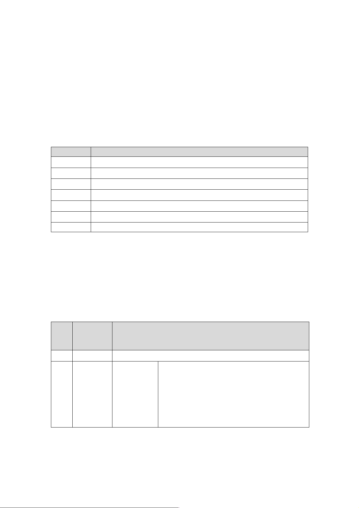
Terms Description
AT Attention Command
GPIO General Purpose I/O
PC Personal Computer
WCDMA Wideband Code Division Multiple Access
UART Universal Asynchronous Receiver/Transmitter
USB Universal Serial Bus
USIM Universal Subscriber Identity Module
Express 1-1
1.3 References
《1424-LZN9012499_U335_Product_Overview_DESC_Rev_C》
2、、、、Product Features
2.1 Product Features List
Platform Features
m
Specificati
on
Description
Ite
1 Chipset STE M340
Quad-band
E-GSM850:824 ~848MHz; 869~893MHz
E-GSM900:880~915MHz; 925~960MHz
2
Frenquenc
y
GSM
DCS1800:1710~1785MHz;
1805~1880MHz
DCS1900:1850~1910MHz;
1930~1990MHz
Page 4
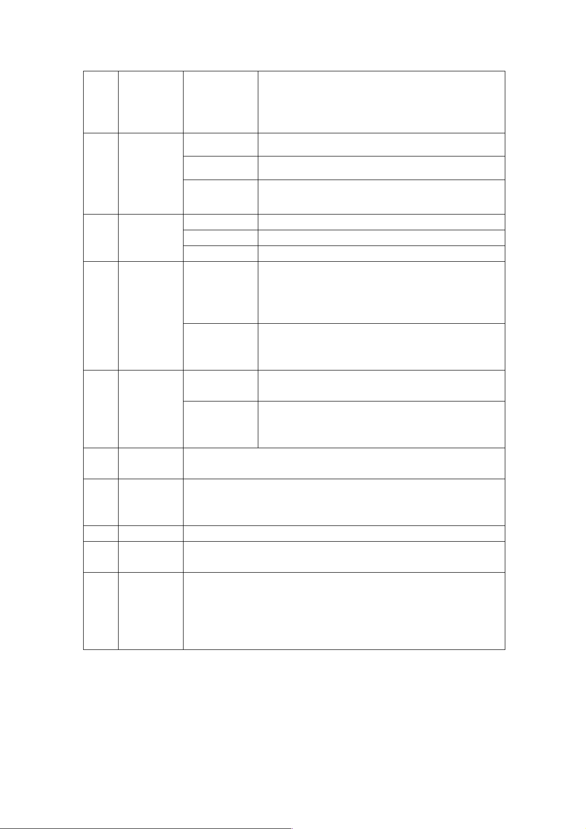
Band I.:1920~1980MHz; 2110~2170MHz
WCDMA
GPRS Multi-slot class 11
Band II.:1850~1910MHz;
1930~1990MHz
Band V.: 824~849MHz; 869~894MHz
3 Data Rate
Modulatio
4
n
5 RF (send)
RF
6
(receive)
Flight
7
Mode
8 USIM
9 Interface Mini-PCI-E
10
11
2.2 Hardware Features
AT
Command
Text
Masseging
EDGE Multi-slot class 11
WCDMA
GSM GMSK - CS1~CS4
EDGE 8PSK - MCS1~CS9
WCDMA HSUPA - 2.0M
GSM
WCDMA
GSM
WCDMA
Support the AT command set or hardware set flight mode
1 Support 1.8V and 3V SIM cards
2 Support SIM Toolkit, consistent with SAT Class3, GSM
11.14 Release 9
Supports 3GPP TS27.005;3GPP TS27.007;ITU-T V.25ter
Support 3GPP TS27.010 serial port multiplexer
1 Supports MT, MO, CB SMS
2 Supports TEXT and PDU SMS format
3 Support CSD and GPRS transmission, and supports the
user default transfer mode
4 Support SMS saving to the USIM card
Uplink:2.0M/384/64Kbps - HSUPA
Downlink:7.2M/384/128Kbps - HSDPA
E-GSM900(GMSK): 33dBm±2db
E-GSM850(8-PSK): 27dBm ±3db
DCS1800(GMSK): 30dBm ±2db
DCS1800(8-PSK): 26dBm +3/-4db
WCDMA: 1920~1980MHz: 27dBm+1/-3db
WCDMA: 1850~1910MHz: 27dBm+1/-3db
WCDMA: 824~849MHz: 27dBm+1/-3db
E-GSM900: -106dBm
DCS1800: -106dBm
WCDMA: Band I: -108dBm
WCDMA: Band II: -108dBm
WCDMA:Band V:-108dBm
Table 2-1
Based on M340 W668 platform. The hardware system block diagram is as
follows,
Page 5
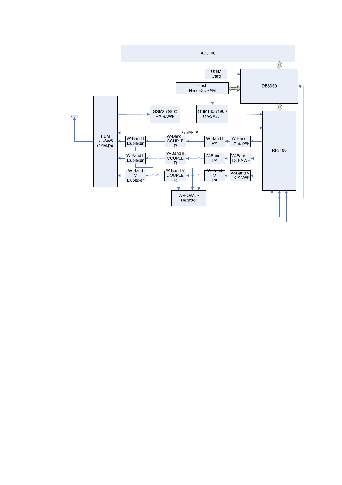
Figure 2-2
Key components description:
RF: GSM and TD of the RF share the same Transceiver, including the
following parts.
Transceiver: RF3400 modulates both GSM and WCDMA RF signal. It also
supports 8PSK modulation of EDGE-WCDMA, HSUPA signal and modulation.
FEM:
1.From the GSM Transceiver RF signal power amplifier to support GMSK and
8PSK modes to achieve GSM-PA function;
2. Send and receive signals from various quarters of the WCDMA,managed
to achieve an antenna switch function.
WCDMA-PA: a total of three chips, respectively, from the Transceiver's I, II,
V-band RF for power amplification, with three operating modes and high
amplification efficiency.
Page 6

Base Band
Digital baseband processor: The DB3350 baseband processor, the internal
integration ARM926EJ, contains numbers of peripherals extensional possibilities
& integrated communication DSP, to achieve the machine's control,
communications protocol processing, and external interface.
Analog baseband processor: The AB3100, the corresponding control voltage for
each group, using I2C interface.
2.3 Software
W668 based on T3G M340's 3G-based program, its software system block
diagram below, the software is divided into three layers:
Abstraction Layer
Abstract hardware processing interface to manage all hardware access, so that
the upper set of software interfaces to use the sameaccess to all hardware
devices, shielding a variety of hardware differences.
Service processing layer
Service processes is to provide services mainly to the outer layer, such as
wireless services, file system services.
Application service layer
Application service is to provide AT commands and other multimedia
applications.
Page 7
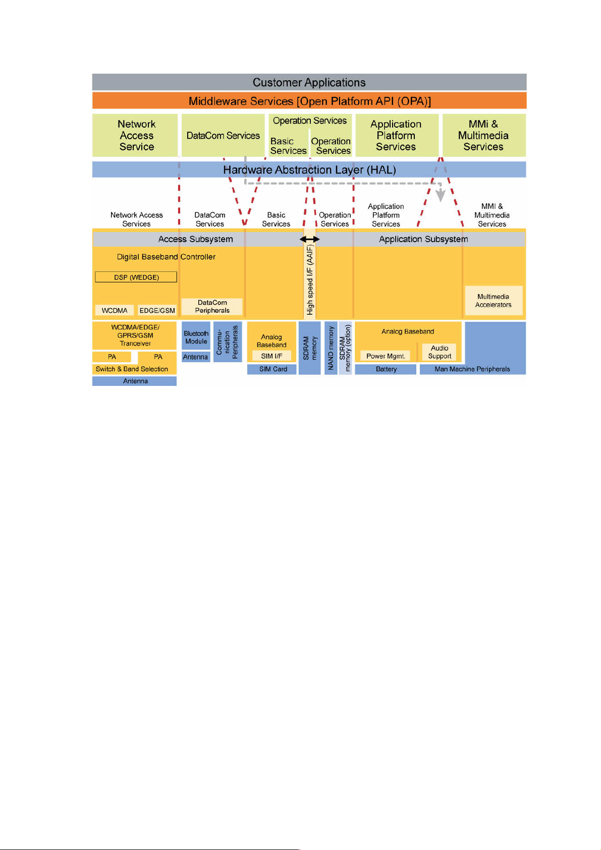
Table 2-3
Page 8
3、、、、Product Specification
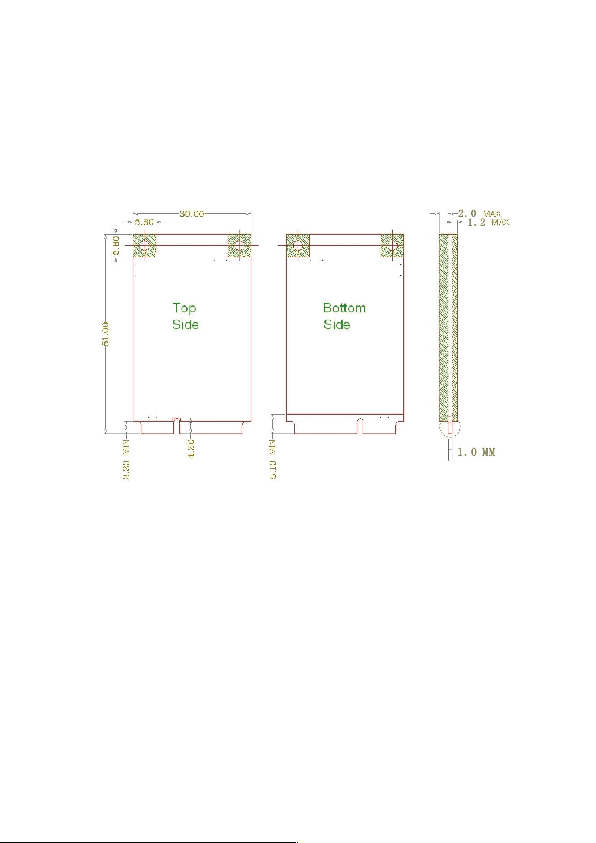
3.1 External Form Structure
The Physical W668 structure dimension is: length 51 +/- 0.2 mms ; high 30
+/- 0.1 mms; thickness 0.2 mm for 4.2 +/-. The dimensions are 51 mmsX30
mmsX4.2 mms, the assembling altitude maximum is 4.2. See figure below,
Figure 3-1
3.2 Interface Description
3.2.1 Interface definition
Through the standard MINI-PCIe interfaces, W668 hardware can connect with
external systems, external systems through the W668's software interface
module communication with the W668, W668 used to provide 3G wireless
communications. To describe conveniently, we call the external system to the
host system.
Page 9
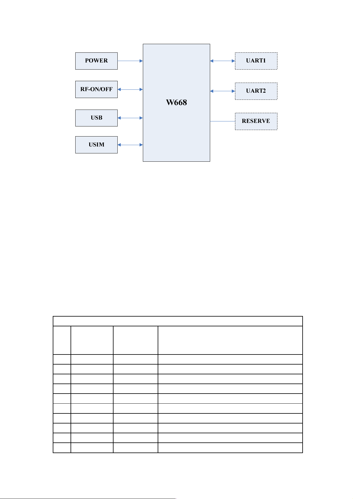
Table 3-2
W668's interface, as shown above, the interface is divided into the following
categories:
Ower Interface
USB Interface
RF Swift Interface
USIM Interface
2 UART interfaces reserved for test points
Spare interface
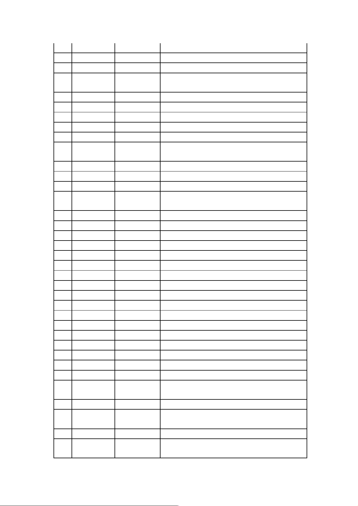
3.2.2 PIN definition
W668 with the host system connection 52PINS pin defined as follows:
W668 Mini PCI Express PIN Define
PI
N
#
standard
descriptio
n
W688 pin
descriptio
n Additional Description
1 WAKE# NC No Connect
2 3.3Vaux VCC_3V3 3.3V DC supply rail from the PC side.
3 COEX1 NC No Connect
4 GND GND Mini Card ground.
5 COEX2 NC No Connect.
6 1.5V NC No Connect
7 CLKREQ# NC No Connect
8 UIM_PWR UIM_PWR Power source for external UIM/SIM.
9 GND GND Mini Card ground.
10 UIM_DATA UIM_DATA External UIM/SIM data signal.
Page 10
11 REFCLK- NC No Connect
12 UIM_CLK UIM_CLK External UIM/SIM clock signal.
13 REFCLK+ NC No Connect
UIM_RESE
14
T UIM_RESET
External UIM/SIM reset signal.
15 GND GND Mini Card ground.
16 UIM_Vpp NC No Connect
17 Reserved NC No Connect
18 GND GND Mini Card ground.
19 Reserved NC No Connect
20
W_DISABL
E#
W_DISABLE
_N For close wireless communications
21 GND GND Mini Card ground.
22 PERST# PERST# Force a hardware reset on the card.
23 PERn0 NC No Connect
3.3Vaux/N
24
C NC No Connect
25 PERp0 NC No Connect
26 GND GND Mini Card ground.
27 GND GND Mini Card ground.
28 1.5V NC No Connect
29 GND GND Mini Card ground.
30 SMB_CLK NC No Connect
31 PETn0 NC No Connect
32 SMB_DATA NC No Connect
33 PETp0 NC No Connect
34 GND GND Mini Card ground.
35 GND GND Mini Card ground.
36 USB_D- USB_D- USB signal D-.
37 GND GND GND
38 USB_D+ USB_D+ USB signal D+.
39 3.3Vaux VCC_3V3 3.3V DC supply rail from the PC side.
40 CPUSB# GND GND
41 3.3Vaux VCC_3V3 3.3V DC supply rail from the PC side.
LED_WWA
42
N# LED_WWAN
Active-low LED signal for indicating the
state of the card.
43 GND GND GND
LED_WLAN
44
# NC No Connect.
45 Reserved NC No Connect.
LED_WPAN
46
# NC No Connect.
Page 11
47 Reserved NC No Connect.
48 1.5V NC No Connect
49 Reserved NC No Connect
50 GND GND Mini Card Ground
51 Reserved NC No Connect
52 3.3Vaux VCC_3V3 3.3V DC supply rail from the PC side.
3.3 Interface Application
3.3.1 Power Interface
W668 single power supply. The rated working voltage is 3.3V.
Work Mode
According to the system's status and power differences, W668 work
modules as shown in Table 3-2.
Woke
Mode
Work
Mode
Standby
Mode
Sleep
Mode
Pin Definition
W668 is part of the system set up four special power as the Vcc inputpins, 14
ground pin GND, 1 RF switch input signal and an LEDindicator signal. See Table
3-3.
Signal Name Pro
VCC_3V3 Pow
GND Gro
W_DISABLE_IN Inp
LED Out
System is in state of telecommunication services.
telecommunication services are being processed.
The system is ready, waiting to enter service mode, sleep mode or
off mode
Parts of the system is turned off. This state is the lowest power
consumption.
Pin position Description Paramet
pert
ies
2,,39,41,52 DC power input 3.3V
er
4,9,15,18,21,26,27,29,
und
ut
put
34,
35,37,40,43,50
Desceiption
Express 3-4
Group
20 Close RF to enter
the sleep
42 LED indicates the
working status
Express 3-5
ers
Page 12

3.3.2 USB Interface
W668 has a USB interface for USB DEVICE device, which can be used as
communications, downloads, and calibration. It follows the USB2.0 protocol
specification. It has the maximum rate to support high-speed 480 Mb / s.
PIN Definition
W668's mini-PCI-E interface with 3.3V power supply. It automatic conversion by
the module internal power supply voltage to the USB. USBDB and USBDM
differential lines for data transmission, as shown in Table 3-5.
Signal
Name
USBDP Input/
Propert
ies
Pin
Description Parameters
position
38 USB differential data lines
Output
USBDM Input/
36 USB differential data lines
Output
Express 3-6
USB Communication
Virtual USB MODEM device for the two commands and data communications.
USB Download And Calibration
USB download and calibration need to elicit the corresponding pin. And then the
signal corresponding to the same PC connected, and then download and install
the appropriate PC-side tools with calibration.
3.3.3 RF Switch Interface
W668 use 2 ways for RF wake-up mechanism to close or open. One is with AT
command and control and the other is with the hardware switch.
Pin Definition
W668 define the following control on the hardware interface: when the external
input to the pin is low, e.g. to ground, the PIN began to process part of the work
to shutting down the radio, so that the device goes to sleep mode.
Page 13
Signal Name Prop
ertie
s
W_DISABLE_N Outp
ut
3.3.4 USIM Interface
W668 provides a SIM card interface, supporting 1.8V and 3.0V, the ICcard is
compatible with ISO7816 standards.
PIN definition
USIM card pin definition USIM_POWER, USIM_DATA, USIM_CLK, USIM_RST,, as
shown in Table 3-8.
Pin
position
20 RF control is working or not. And
then go to sleep.
Express 3-7
Description Parame
ters
Signal Name Propert
ies
USIM_POWER Output
USIM_DATA Input/
Output
USIM_CLK Output
USIM_RST Output
Pin
position
8 USIM card Power supply 1.8V/3V
10 USIM card data
12 Usim card clock
14 Usim card reset signal
Express 3-8
Description Parameters
Page 14
4、、、、Mechanical Properties
4.1 Mini-PCI-E
W668 uses a 52pin Goldfinger to connect to devices. The thickness of goldfinger
is 1.0 ± 0.2mm. The spacing is 0.2mm. The dimensions is conpliant to standard
mini-PCI-Einterface specification.
4.2 RF connector
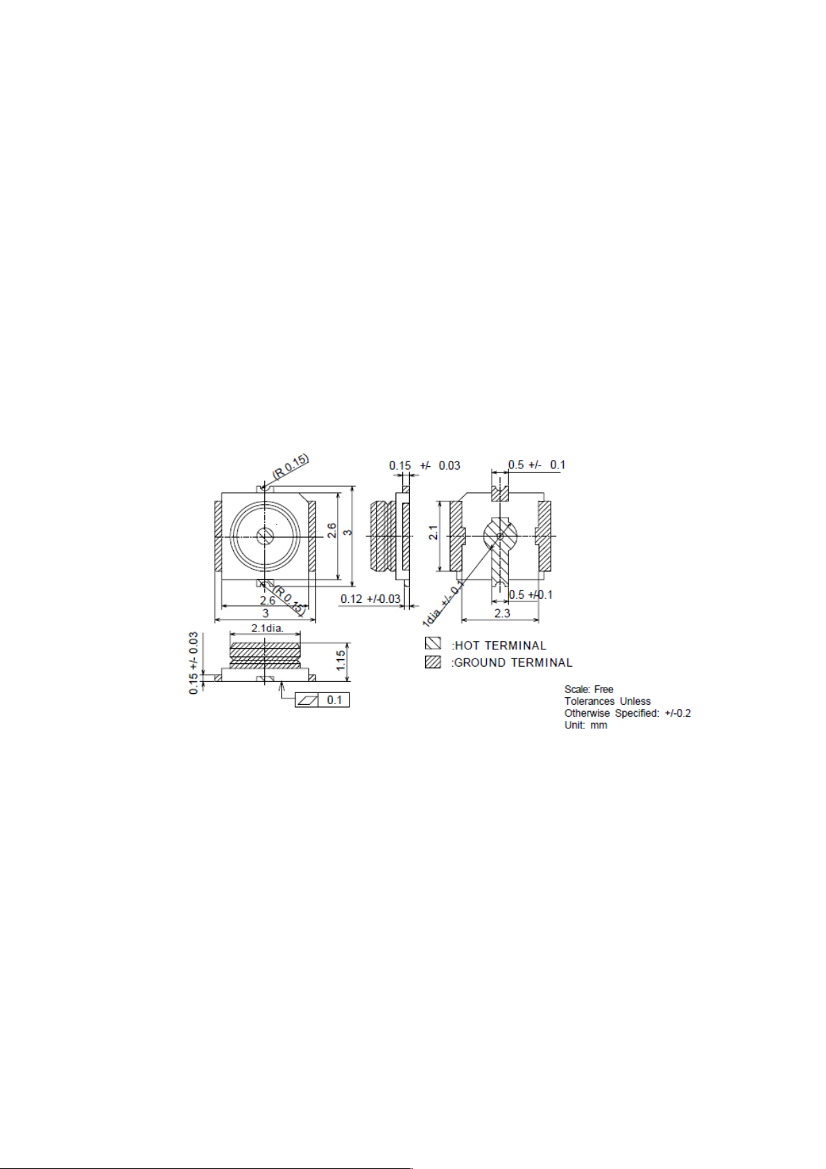
RF antenna connector includes a connector and cable to match.W668's RF
connector is murata's MM9329-2700 with the size specifications below:
Figure 4-1
4.2.1 Antenna cable
And W668 RF cable connectors to match a lot of kinds. customers can choose
according to actual situation.
Page 15
5、、、、Electrical Characteristics
5.1 Limits voltage range
Parameters
V3.3_IN -0.3 3.3 3.5 V
V3.3_IN_REV -0.3 3.3 3.5 V
VSIM -0.3 1.8/3.0 1.8/3.0+0.3 V
5.2 Operating voltage range
3.3~3.5V
5.3 Current.
Current:
Standby:<3mA
5.4 RF indicator
5.4.1 GSM/GPRS/EDGEF indicator
Frequency
Min Rating Max Units
Table 5-1
E-GSM900 TX: 880-915MHz RX: 925-960MHz
DCS1800 TX: 1710-1785MHz RX: 1805-1880MHz
Transmitter Indicator
A) Transmitting Carrier Peak Power
POWER
CONTRO
L LEVEL
0
1
2
3
4
5 33 ±0.2 ±0.3 20 ±0.2 ±2
6 31 ±0.2 ±2 18 ±0.2 ±2
7 29 ±0.2 ±2 16 ±0.2 ±2
tandard
value
(dBm)
E-GSM900(dBm) DCS1800 (dBm)
Calibratio
n range
30 ±0.2 ±0.3
28 ±0.2 ±2
24 ±0.2 ±2
22 ±0.2 ±2
Limits
tandard
value
(dBm)
26 ±0.2 ±2
Calibrati
on range
Limits
8 27 ±0.2 ±2 14 ±0.2 ±2
Page 16
9 25 ±0.2 ±2 12 ±0.2 ±2
10 23 ±0.2 ±2 10 ±0.2 ±2
11 21 ±0.2 ±2 8 ±0.3 ±2
12 19 ±0.2 ±2 7 ±0.4 ±2
13 17 ±0.2 ±2 6 ±0.5 ±2
14 15 ±0.2 ±2 5 ±0.5 ±2
15 13 ±0.2 ±2 3 ±0.8 ±2
16 11 ±0.2 ±2
17 9 ±0.2 ±2
18 7 ±0.4 ±2
19 5 ±0.5 ±2
Table 6-1
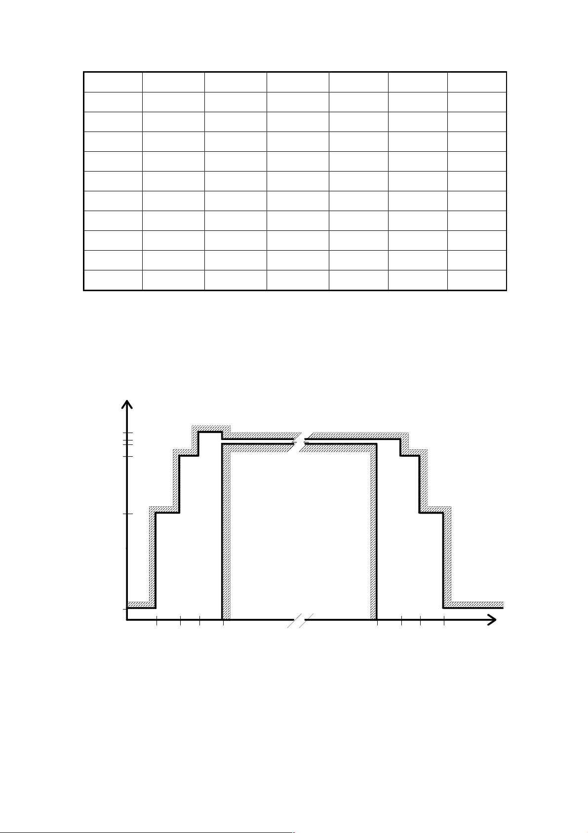
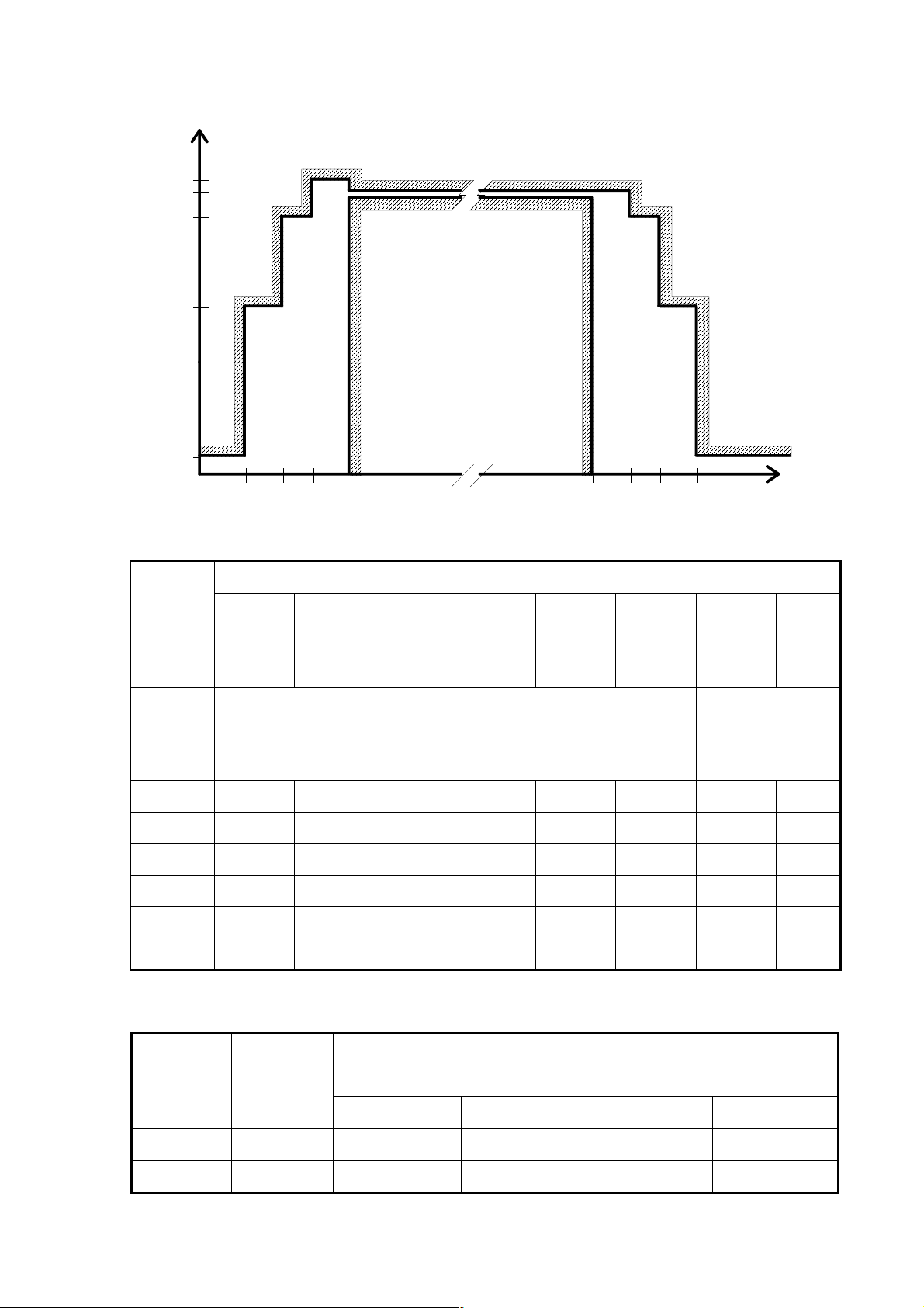
B) Launch of The Carrier Frequency
Emergency provisions of conventional GSM power / time
maskrequirements of Figure 5-1 frame, the provisions on access to
emergency power / time mask requirements box shown in Figure 5-2.
dB
+ 4
+ 1
- 1
- 6
(**)
- 30
(***)
(147 bits)
(*)
10
祍
8 祍10
祍
7056/13 (542.8)
祍
10 祍8
祍
10
祍
Figure 5-1
t
Page 17
dB
+ 4
+ 1
- 1
- 6
(**)
- 30
(***)
(*)
10
祍
8 祍10
祍
C) Modulation Spectrum
(87 bits)
4176/13 (321.2) 10
10 祍8
祍祍
Figure 5-2
祍
t
Offset at the specified maximum relative level (dB)
Power
600~
1200~
1800~
level
100KHz 200KHz 250KHz 400KHz
<1200
<1800
<6000
(dBm)
KHz
KHz
KHz
Measurement
Measurement bandwidth 30KHz
bandwidth100K
Hz
>43 +0.5 -30 -33 -60 -70 -73 -75 -80
41
39
37
35
<33
+0.5 -30
+0.5 -30
+0.5 -30
+0.5 -30
+0.5 -30
-33 -60 -68 -71 -73 -80
-33 -60 -66 -69 -71 -80
-33 -60 -64 -67 -69 -80
-33 -60 -62 -65 -67 -80
-33 -60 -60 -63 -65 -80
Express 6-2
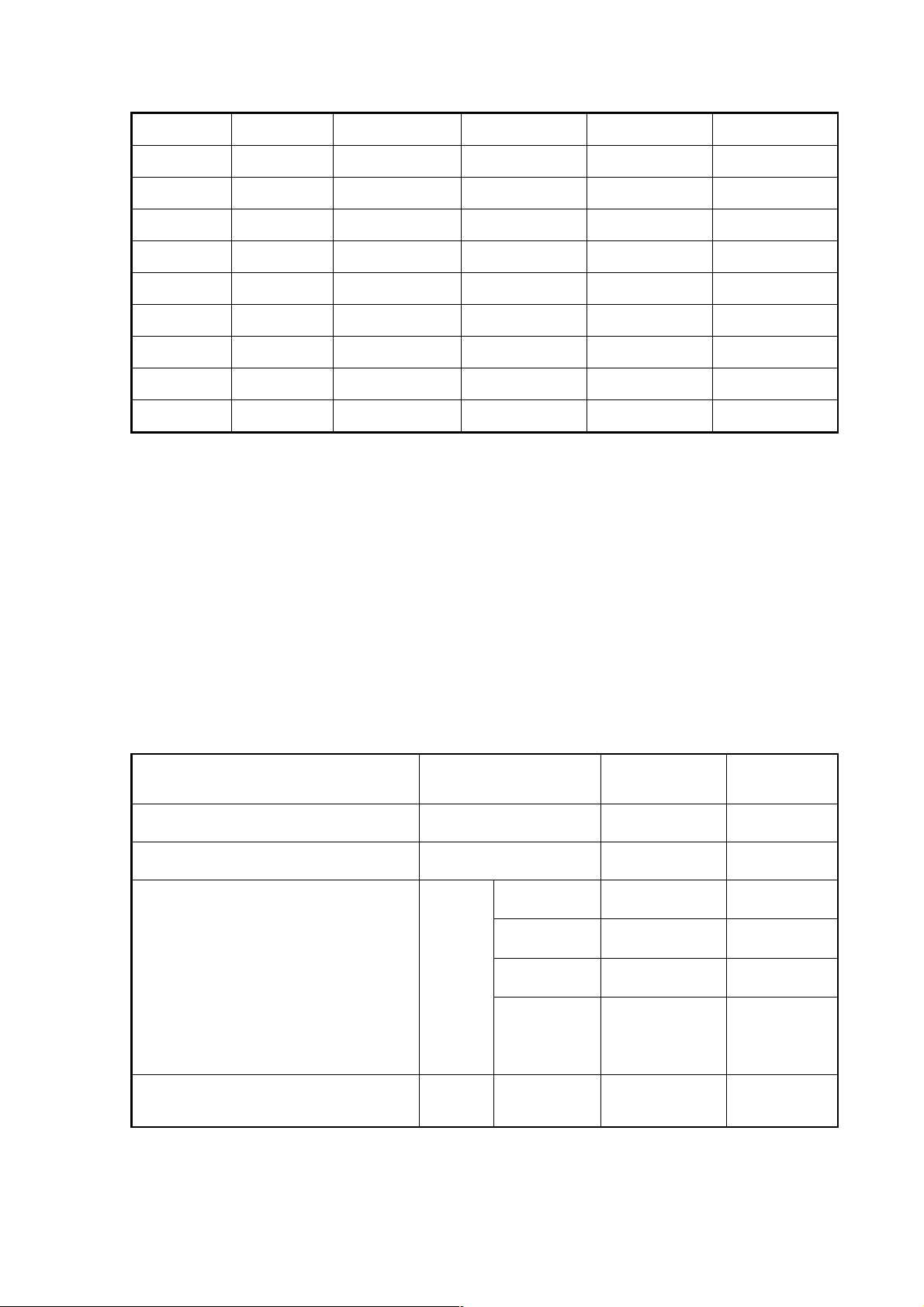
D) Switch Spectrum
6000
KHz
Power
Different from the carrier frequency offset at the maximum
wer level
control
power (dBm)
(dBm)
level
400KHz 600KHz 1200KHz 1800KHz
0 43 -9 -21 -21 -24
1 41 -11 -21 -21 -24
Page 18
2 39 -13 -21 -21 -24
3 37 -15 -21 -21 -24
4 35 -17 -21 -21 -24
5 33 -19 -21 -21 -24
6 31 -21 -23 -23 -26
7 29 -23 -25 -25 -28
8 27 -23 -26 -27 -30
9 25 -23 -26 -29 -32
10 23 -23 -26 -31 -34
≥11 21 -23 -26 -32 -36
Express 6-3
E) Fquency Tolerance
Fquency Tolerance < 0.1ppm。
F) Phase Tolerance
RMS for each burst is less than 5 °. The maximum peak of each burst
phase error should not exceed 20 °.
G) Conducted Spurious Emissions
Measurement Bandwidth
Frequency Band
100kHz~50MHz — 10kHz 30kHz
50~500MHz — 100kHz 300kHz
500MHz ~ 12.75GHz,
Does not contain the following
and the corresponding transmit
and receive frequency bands
P-GSM890 ~ 915 and 935 ~
960MHz,
DCS1710 ~ 1785 and 1805 ~
1880MHz
P-GSM:890~915MHz
E-GSM:880~915MHz
Frequency
Deviation
From
the
phase
Should
be the
Launc
h
Band
From
the
0~10MHz 100 kHz 300 kHz
≥10MHz 300 kHz 1MHz
≥20MHz 1MHz 3MHz
≥30MHz 3MHz 3MHz
1.8~6.0M
Hz
Measuremen
t Bandwidth
30kHz 100 kHz
Video
Bandwidth
Page 19
DCS:1710~1785MHz
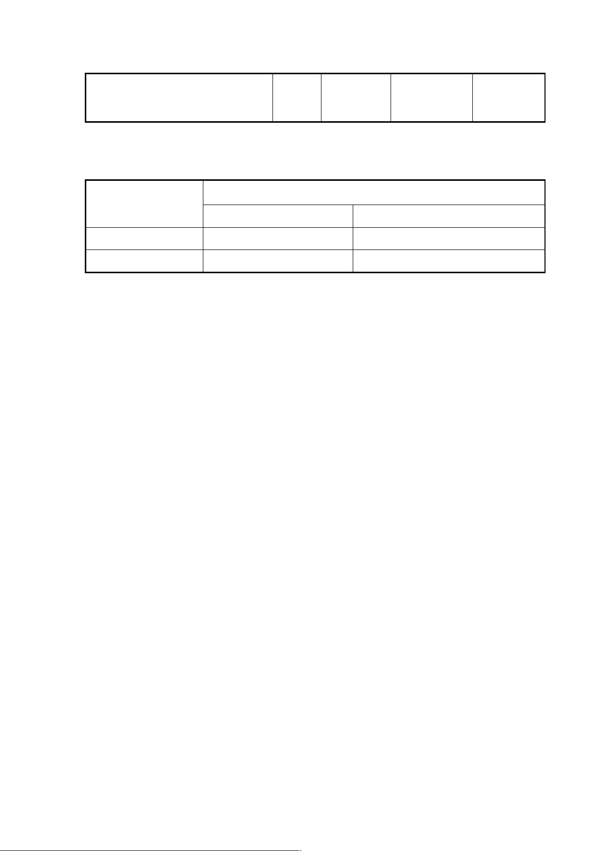
Technical Requirements
Frequency Range
E-GSM 850/900MHz DCS 1800/PCS1900MHz
0.1 – 1000MHz -36 -36
1000 – 12750MHz -30 -30
Receiver Index
Static Reference Sensitivity Is As Follows:
E-GSM900 < -106dBm (BER <2.4%)
DCS1800 < -106dBm (BER <2.4%)
carrier
freque
ncy
Express 6-3
Spurious Power Levels (dBm)
Express 6-3
>6.0MHz 100kHz 300kHz
5.4.2 WCDMA RF Index
Operating Frequency Range
Band I:2110~2170MHz
Band II:1930~1990MHz
Band V:869~894 MHz
Transmitter Indicators Index
A) Output Power
Max output power: 27dBm +1dB /-3dB
Min output power:≤-49dBm
B)Adjacent Channel Leakage Power Ratio
C) EVM Tolerance
D) Stray Radiation
Receiver Index
A) Reference sensitivity
B) Maximum input level
C) ACS adjacent channel selectivity
D) Blocking characteristics...
E) Spurious response
Page 20

6、Evironmental Characteristics
6.1 Temperature
W668 work or storage temperature required to achieve the following criteria:
Parameters
Operating
Min Rating Max Units
-20 +25 +70 ℃
Temperature
Storage
-45 --- +85 ℃
Temperature
Express 6-1
6.2 Humidity
W668 requires relative humidity of 5 to 95% relative humidity, non-condensing
surface.
7、Validation test
 Loading...