

Page 1

Anybus®CompactCom™B40 Modbus Serial
USER MANUAL
SCM-1202-130 1.1 en-US ENGLISH
Page 2

Important User Information
Disclaimer
The information in this document is for informational purposes only. Please inform HMS Industrial Networks of any
inaccuracies or omissions found in this document. HMS Industrial Networks disclaims any responsibility or liability
for any errors that may appear in this document.
HMS Industrial Networks reserves the right to modify its products in line with its policy of continuous product
development. The information in this document shall therefore not be construed as a commitment on the part of
HMS Industrial Networks and is subject to change without notice. HMS Industrial Networks makes no commitment
to update or keep current the information in this document.
The data, examples and illustrations found in this document are included for illustrative purposes and are only
intended to help improve understanding of the functionality and handling of the product. In view of the wide range
of possible applications of the product, and because of the many variables and requirements associated with any
particular implementation, HMS Industrial Networks cannot assume responsibility or liability for actual use based on
the data, examples or illustrations included in this document nor for any damages incurred during installation of the
product. Those responsible for the use of the product must acquire sufficient knowledge in order to ensure that the
product is used correctly in their specific application and that the application meets all performance and safety
requirements including any applicable laws, regulations, codes and standards. Further, HMS Industrial Networks will
under no circumstances assume liability or responsibility for any problems that may arise as a result from the use of
undocumented features or functional side effects found outside the documented scope of the product. The effects
caused by any direct or indirect use of such aspects of the product are undefined and may include e.g. compatibility
issues and stability issues.
Anybus®CompactCom™B40 Modbus Serial User Manual
SCM-1202-130 1.1 en-US
Page 3

Table of Contents
Page
1 Preface ................................................................................................................................. 3
1.1 About this Document........................................................................................................ 3
1.2 Document History ............................................................................................................ 3
1.3 Document Conventions.....................................................................................................3
1.4 Document Specific Conventions.......................................................................................... 4
1.5 Trademark Information ..................................................................................................... 4
2 About the Anybus CompactCom B40 Modbus Serial........................................................ 5
2.1 General Information ......................................................................................................... 5
2.2 Features ......................................................................................................................... 6
2.3 Overview........................................................................................................................ 6
2.4 How to Use this Manual .................................................................................................... 6
3 Modbus Application Interface............................................................................................ 8
3.1 How To Set Up and Initialize the Modbus Communication ......................................................8
3.2 Supported Modbus Commands ........................................................................................ 10
3.3 Modbus Register Map..................................................................................................... 11
4 Hardware Design ............................................................................................................... 13
4.1 Host Application Interface ............................................................................................... 13
4.2 Network Connector ........................................................................................................ 21
4.3 Network Configuration Switches ....................................................................................... 28
4.4 IO Expansion Mechanism................................................................................................. 29
A Technical Specification...................................................................................................... 31
A.1 Environmental............................................................................................................... 31
A.2 Shock and Vibration ....................................................................................................... 31
A.3 Electrical Characteristics.................................................................................................. 31
A.4 Regulatory Compliance ................................................................................................... 32
B Mechanical Specification .................................................................................................. 33
B.1 Anybus CompactCom B40 Modbus Serial ........................................................................... 33
B.2 Footprint ...................................................................................................................... 34
B.3 Height Restrictions ......................................................................................................... 34
B.4 Network Connector Boards (Optional) ............................................................................... 35
B.5 Connector Board for Fiber Optic Ethernet .......................................................................... 35
B.6 Assembly ...................................................................................................................... 37
Anybus®CompactCom™B40 Modbus Serial User Manual
SCM-1202-130 1.1 en-US
Page 4

C Firmware Upgrade ............................................................................................................ 39
C.1 Using Firmware Manager II .............................................................................................. 40
C.2 Using FTP ..................................................................................................................... 41
D The Anybus State Machine ............................................................................................... 42
D.1 General Information ....................................................................................................... 42
D.2 State Dependent Actions ................................................................................................. 43
E Implementation Guidelines .............................................................................................. 44
E.1 General ........................................................................................................................ 44
E.2 Example ....................................................................................................................... 44
E.3 Power Supply Considerations ........................................................................................... 45
F Network Interface Examples ............................................................................................ 47
Anybus®CompactCom™B40 Modbus Serial User Manual
SCM-1202-130 1.1 en-US
Page 5

Preface 3 (48)
1 Preface
1.1 About this Document
This document is intended to provide a good understanding of the functionality offered by the
Anybus CompactCom B40 Modbus Serial.
The reader of this document is expected to be familiar with high level software design and
communication systems in general. The information in this user manual should normally be
sufficient to implement a design. However if advanced network specific functionality is to be
used, in-depth knowledge of network networking internals and/or information from the official
network specifications may be required. In such cases, the persons responsible for the
implementation of this product should either obtain the network specification to gain sufficient
knowledge or limit their implementation in such a way that this is not necessary.
For additional information, please visit the support website at www.anybus.com/support.
1.2 Document History
Version
1.0 2019-04-30
1.1 2019-05-16
Date
1.3 Document Conventions
Ordered lists are used for instructions that must be carried out in sequence:
1. First do this
2. Then do this
Unordered (bulleted) lists are used for:
• Itemized information
• Instructions that can be carried out in any order
...and for action-result type instructions:
► This action...
→ leads to this result
Bold typeface indicates interactive parts such as connectors and switches on the hardware, or
menus and buttons in a graphical user interface.
Monospaced text is used to indicate program code and other
kinds of data input/output such as configuration scripts.
Description
First release
Updated for PROFINET release
This is a cross-reference within this document: Document Conventions, p. 3
This is an external link (URL): www.hms-networks.com
This is additional information which may facilitate installation and/or operation.
This instruction must be followed to avoid a risk of reduced functionality and/or damage
to the equipment, or to avoid a network security risk.
Anybus®CompactCom™B40 Modbus Serial User Manual
SCM-1202-130 1.1 en-US
Page 6

Preface 4 (48)
Caution
This instruction must be followed to avoid a risk of personal injury.
WARNING
This instruction must be followed to avoid a risk of death or serious injury.
1.4 Document Specific Conventions
• The terms “Anybus” or “module” refers to the Anybus CompactCom module.
• The terms “host” or “host application” refer to the device that hosts the Anybus.
• Hexadecimal values are written in the format NNNNh or 0xNNNN, where NNNN is the
hexadecimal value.
• A byte always consists of 8 bits.
• All dimensions in this document have a tolerance of ±0.10 mm unless otherwise stated.
• Outputs are TTL compliant unless otherwise stated.
• Signals which are “pulled to GND” are connected to GND via a resistor.
• Signals which are “pulled to 3V3” are connected to 3V3 via a resistor.
• Signals which are “tied to GND” are directly connected to GND,
• Signals which are “tied to 3V3” are directly connected to 3V3.
1.4.1 Pin Types
The pin types of the connectors are defined in the table below. The pin type may be different
depending on which mode is used.
Pin type
I Input
O Output
I/O Input/Output (bidirectional)
OD Open Drain
Power
Definition
Pin connected directly to module power supply, GND or 3V3
1.5 Trademark Information
Anybus®is a registered trademark of HMS Industrial Networks.
EtherNet/IP is a trademark of ODVA, Inc.
All other trademarks are the property of their respective holders.
Anybus®CompactCom™B40 Modbus Serial User Manual
SCM-1202-130 1.1 en-US
Page 7

About the Anybus CompactCom B40 Modbus Serial 5 (48)
2 About the Anybus CompactCom B40 Modbus Serial
2.1 General Information
The Anybus CompactCom B40 Modbus Serial is a communication solution for simple industrial
field devices. The host application communicates with the product using the Modbus RTU
protocol. The Anybus CompactCom B40 Modbus Serial then communicates the data to the
network. Typical applications are basic level I/O blocks, temperature controllers, measuring
devices, and sensors.
The Anybus CompactCom B40 Modbus Serial software interface is designed to be network
protocol independent, making it possible to support several networking systems using the same
application software code/driver.
The Anybus CompactCom B40 Modbus Serial share footprint and electrical interface with the
other members of the product family, independent of fieldbus or network. The host application
connector provides an interface between the host application (Modbus RTU) and the Anybus
CompactCom, while the network connector provides access to the chosen network. The Anybus
CompactCom acts as a Modbus RTU slave on the host application side.
The Anybus CompactCom 40 family offers a wide range of functionality. For advanced products and
applications, we recommend the standard Anybus CompactCom 40.
For general information about other products using the Anybus CompactCom 40 platform,
consult www.anybus.com/support.
This a class A product. In a domestic environment, this product may cause radio
interference in which case the user may be required to take adequate measures.
This product contains ESD (Electrostatic Discharge) sensitive parts that may be damaged if
ESD control procedures are not followed. Static control precautions are required when
handling the product. Failure to observe this may cause damage to the product.
Anybus®CompactCom™B40 Modbus Serial User Manual
SCM-1202-130 1.1 en-US
Page 8
About the Anybus CompactCom B40 Modbus Serial 6 (48)
Host processor
with applicaon
Anybus
CompactCom
Modbus
Serial
Process DataData
Industrial Network
Modbus RTU
2.2 Features
• Simple implementation and great connectivity flexibility
• Serial Communications Interface (UART), that can be connected to almost any standard
microcontroller
• Standard Modbus RTU serial protocol
• Galvanic isolation integrated
• Low power consumption
• Control pins for status indications according to each network standard
• Separate network connector board available
• Precompliance tested for network conformance (where applicable).
• Precompliance tested for CE & UL. Contact HMS Industrial Networks for further information.
All Anybus CompactCom 40 Modbus Serial will be precertified for network conformance.
This is done to ensure that the final product can be certified, but it does not necessarily
mean that the final product does not require recertification. Contact HMS Industrial
Networks for further information.
2.3 Overview
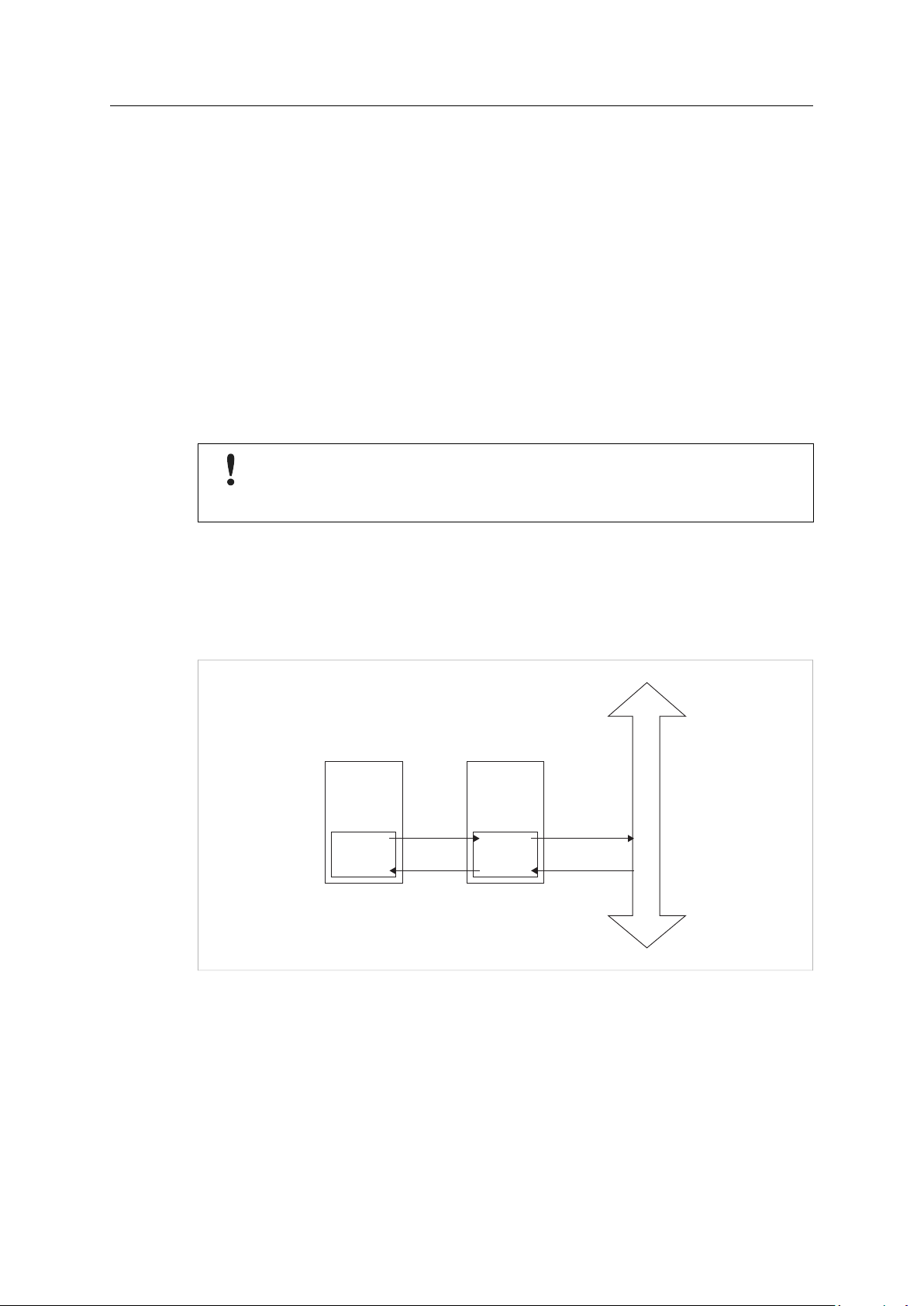
The picture below shows the data flow in the Anybus CompactCom B40 Modbus Serial. The
application sets up the Modbus RTU communication, and the Anybus CompactCom maps the
process data to the industrial network/fieldbus.
Fig. 1
2.4 How to Use this Manual
This manual includes the following:
1. The implemented Modbus RTU application interface and how to use it (host application).
2. Instructions on how to indesign the Anybus CompactCom in your product (hardware design).
Network specific configuration, performed from the network, is described in the Anybus
CompactCom 40 Modbus Serial Network Guides.
Anybus®CompactCom™B40 Modbus Serial User Manual
SCM-1202-130 1.1 en-US
Page 9

About the Anybus CompactCom B40 Modbus Serial 7 (48)
2.4.1 Host Application
The Modbus application interface is set up and configured in the same way, independent of
which network the data will be sent to/read from. This process, including an example is
described in Modbus Application Interface, p. 8.
2.4.2 Hardware Design
• When creating your hardware design, refer to Hardware Design, p. 13 for descriptions of
connectors etc. Please note that some inputs should be strapped to ensure correct behavior.
• Dimensions and other mechanical information is presented in Mechanical Specification, p.
33.
• Technical specifications, like temperature limits and electrical specifications, are given in
Technical Specification, p. 31.
Anybus®CompactCom™B40 Modbus Serial User Manual
SCM-1202-130 1.1 en-US
Page 10

Modbus Application Interface 8 (48)
3 Modbus Application Interface
The host application interface of the product consists of a Modbus Serial interface, which
implements a reduced set of registers and commands. The Anybus CompactCom acts as a
Modbus RTU slave.
3.1 How To Set Up and Initialize the Modbus Communication
To set up and initialize the communication between the host application and the network, follow
the steps below. Steps 2 - 6 includes examples of what the Modbus messages can look like.
1. Set Modbus address, baud rate, stop bits, and parity according to Communication Settings,
p. 19.
See Hardware Design, p. 13 for information on how to connect the corresponding pins.
2. Write initial values to the Write Process Data area (registers 0x0000-). (Optional)
Example – Using the Modbus function Write Multiple Holding Registers to set
initial values for 10 Write Process Data registers (20 bytes) to CompactCom with address 5.
Address Function Code
0x05 16 0x0000 10 20
Data CRC
Starting
Address
Quantity of
Registers
Byte Count
Register
Values
20 bytes of
data
CRC-16-ANSI
3. Write switch settings to register 0x5200-0x5201, “Application switch 1” and “Application
switch 2”. Optional for networks that do not require these settings.
Example – Using the Modbus function Write Single Holding Register to set the
Node Address for a network using a node address for identification. NOTE: Node address 7
will be used on the Industrial Network (e.g. PROFIBUS).
Address Function Code
0x05 6 0x5200 7 CRC-16-ANSI
Data CRC
Register Address Register Value
4. Set Offline Action for Read Process Data in register 0x5101 (Clear or No action). (Oprtional)
Example – Using the Modbus function Write Single Holding Register to configure
Clear as the Offline Action for Read Process Data (all data will be 0 if the network is
offline).
Address Function Code
0x05 6 0x5101 0 CRC-16-ANSI
Data CRC
Register Address Register Value
5. Set the size of the Write Process Data area to register 0x5102. Data type (byte or word) is
configured with register 0x5100.
Example – Using the Modbus function Write Single Holding Register to configure
Write Process Data size 20 bytes. Assuming default value of register 0x5100, i.e. data type is
UINT8.
Address Function Code
0x05 6 0x5102 20 CRC-16-ANSI
Data CRC
Register Address Register Value
®
Anybus
CompactCom™B40 Modbus Serial User Manual
SCM-1202-130 1.1 en-US
Page 11

Modbus Application Interface 9 (48)
6. Set the size of the Read Process Data area to register 0x5103. Data type (byte or word) is
configured with register 0x5100.
Example – Using the Modbus function Write Single Holding Register to configure
Read Process Data size 18 bytes. Assuming default value of register 0x5100, i.e. data type is
UINT8.
Address Function Code
0x05 6 0x5103 18 CRC-16-ANSI
Data CRC
Register Address Register Value
7. The CompactCom is now ready to start communicating with the network master with the
configured settings. Start cyclical read/write of process data to register 0x0000- and 0x1000-.
Also consider to cyclically monitor the values of register 0x0FFD (Anybus Switch Status),
0x0FFE (LED status), and 0x0FFF (Anybus Status).
If a reset request is indicated in the Anybus Status register, the host application must reset
the CompactCom, and start the initialization sequence from step 1. See RESET (Reset Input),
p. 18.
Example – The Modbus function Read/Write Multiple Registers allows you to
both read and write registers with one command. In this example the status registers and
the read process data registers are read, at the same time as the write process data
registers are written.
Command:
Address Function Code
0x05 23 0x0FFD 12 0x0000 10 20
Data CRC
Read
Starting
Address
Quantity
to Read
Write
Starting
Address
Quantity
to Write
Write
Byte
Count
Write
Reg
Values
20 bytes
of data
CRC-16-ANSI
Response:
Address Function Code
0x05 23 24
Data CRC
Read Byte Count Read Reg Values
24 bytes of data
CRC-16-ANSI
The Anybus CompactCom will stay in state SETUP until values have been written to 0x5102 and
0x5103 (items no. 5 and 6 in the list above). The Anybus CompactCom will then change states to
WAIT_PROCESS, and the registers 0x5100-0x5103 will be read-only.
See also ..
• The Anybus State Machine, p. 42
Anybus®CompactCom™B40 Modbus Serial User Manual
SCM-1202-130 1.1 en-US
Page 12

Modbus Application Interface 10 (48)
3.2 Supported Modbus Commands
# Name
3
4
6
16
23
70
Read multiple registers All mapped to the same register space.
Read input registers
Write single register
Write multiple registers
Read/Write registers
Anybus command Custom Modbus command, see below
Description
3.2.1 Error Handling
• Modbus reads, addressing undefined registers, return zeroes.
• Modbus writes, addressing undefined registers, do not return any error.
• Modbus writes containing invalid data to registers do not return any error.
• Modbus writes, addressing read-only registers, do not return any error.
3.2.2 Endianess
• If 8-bit data types are mapped to Modbus registers, the first byte is mapped to LSB and the
second byte is mapped to MSB of the Modbus register.
3.2.3 Anybus Command (Modbus Function Code 70)
This command can be used to send an Anybus CompactCom message. Allowed content depends
on which network is connected to the Anybus CompactCom. The data field part of the telegram
is composed by concatenating the content for each configuration option to include. Note that
the total amount of configuration options to set is limited to 244 bytes of data. Please refer to
the applicable network appendix for more information.
The content of the telegram will be stored and used at the next startup. It is not necessary to
send this telegram at each startup. Instead it is recommended to send it once to customize the
Anybus CompactCom behavior.
Request format:
0 1 2
3 4 5 6 7 8 9 10–n
Address Function Size Data Field CRC
(Address)
70 66 1 1 0 1 7 0
The content of the data field depends on which network is connected. Please refer to the applicable
network appendix for details.
Size of
Data
Field
0
0-244 bytes of
data,
configuring the
Anybus
CompactCom
behavior
(n+1)(n+2)
(CRC)
Response format
0 1 2 3 4 5 6 7 8 9 10–11
Address Function
(Address)
®
Anybus
CompactCom™B40 Modbus Serial User Manual
70 2 1 1 0 17 0 0 0
Size
CRC
(CRC)
SCM-1202-130 1.1 en-US
Page 13

Modbus Application Interface 11 (48)
3.3 Modbus Register Map
The Modbus register space is designed to allow easy and efficient communication using a single
cyclic read/write Modbus command.
Register#
0x0000 -
0x0FFD
0x0FFE LED status
0x0FFF
0x1000 -
0x5003
Name Access
Write process data
Anybus Switch status Read only Value of INPUT1 and INPUT2 pins.
Anybus status
Read process data Read only Area is updated with new data from Network ONLY when address
Module type Read only Anybus CompactCom 40 (0x0403)
Description
Read/
Write
Read only Bit field holding the current state of the network status LEDs as
Read/
Write
When the last byte of mapped process data is written, data is sent
to the network for consistency reasons.
INPUT1:
INPUT2:
follows:
Bit:
b0:
b1:
b2:
b3:
b4:
b5:
b6:
b7:
b8 - b15
Anybus status register with two additional bits, Reset and Set
Default added.
Bit(s)
0 - 2
3 SUP
4 -13
14
15 Reset
0x1000 is read.
LSB
MSB
Contents:
LED1A status (0=OFF, 1=ON)
LED1B status (0=OFF, 1=ON)
LED2A status (0=OFF, 1=ON)
LED2B status (0=OFF, 1=ON)
LED3A status (0=OFF, 1=ON)
LED3B status (0=OFF, 1=ON)
LED4A status (0=OFF, 1=ON)
LED4B status (0=OFF, 1=ON)
(reserved)
Description
Anybus state (See The Anybus State Machine, p. 42)
0. Setup
1: NW_INIT
2: WAIT_PROCESS
3: IDLE
4: PROCESS_ACTIVE
5: ERROR
6: (reserved)
7: EXCEPTION
0: Module is not supervised
1: Module is supervised by another network device
The SUP bit indicates the overall status of the network
communication. For example, on CIP, this bit indicates
that the master has a connection towards the module.
Exactly how this functionality should be handled, the
offered level of security, and how to correctly activate
it is network specific and often depends on external
circumstances, e.g. configuration of the network as
well as other network devices. Whether use of the
SUP-bit is appropriate must therefore be decided for
each specific application and network.
(reserved)
Set Default
0: No action
1: Application is requested to set “factory default” to
all parameters/settings. Application shall acknowledge
this by writing 1 to this bit to clear it.
0: No action
1: Application is requested to reset the Anybus
CompactCom
®
Anybus
CompactCom™B40 Modbus Serial User Manual
SCM-1202-130 1.1 en-US
Page 14

Modbus Application Interface 12 (48)
Register#
0x5004
0x5005
Name Access
Network type Read only
Anybus Exception Code Read only
0x5100 Data type
0x5101
0x5102
Offline action
Number of Write
Parameters
0x5103
Number of Read
Parameters
0x5200
0x5201
Application switch 1
Application switch 2
Read/
Write
Read/
Write
Read/
Write
Read/
Write
Read/
Write
Read/
Write
Description
0x0089:
0x009B:
0x00:
0x01:
0x02:
0x03:
0x04.
0x05:
0x06:
0x07:
0x08:
0x09:
0x0A:
0x0B:
0x0C:
PROFINET IRT
EtherNet/IP
No exception
Application timeout
Invalid device address
Invalid communication settings
Major unrecoverable application event
Waiting for application reset
Invalid process data configuration
Invalid application response
NVS memory checksum error
Functional Safety Module error
Insufficient application implementation
Missing serial number
File system is corrupt
Data type of the parameters that are mapped to Write and Read
process data.
UINT8:
UINT16:
0x0004 (Default)
0x0005
R/W in SETUP state.
Read only in other states.
Action taken when the Anybus CompactCom is not in PROCESS_
ACTIVE state.
0x0000:
0x0001:
Clear “Read Process data area”
No action (Default)
R/W in SETUP state.
Read only in other states.
Number of parameters mapped to Write process data.
If the value written is bigger than module can handle, the value will
automatically be adjusted to max possible value (according to
network) after the SETUP state.
R/W in SETUP state. Read only in other states.
Number of parameters mapped to Read process data.
If the value written is bigger than module can handle, the value will
automatically be adjusted to max possible value (according to
network) after the SETUP state.
R/W in SETUP state. Read only in other states.
This register can be used for the node address.
Value written to this register may be defined by DIP switches on
the application. See Network Configuration Switches, p. 28.
This register can be used for defining stop bits and baud rate.
Value written to this register may be defined by DIP switches on
the application. See Network Configuration Switches, p. 28.
®
Anybus
CompactCom™B40 Modbus Serial User Manual
SCM-1202-130 1.1 en-US
Page 15
Hardware Design 13 (48)
Pin 1
Application
interface
Pin 1
Network
interface
Outline of brick
Top view
4 Hardware Design
Information needed to design the hardware for a product embedding the Anybus CompactCom
B40 Modbus Serialis presented later in this section. This includes mechanical and electrical
specification, connector pinnings etc. An example on how to design a network interface is also
included. An optional connector board is available.
• For the host application and network interfaces, see Hardware Design, p. 13
• For further implementation guidelines see Implementation Guidelines, p. 44
• For brick dimensions, footprint dimensions and height restrictions, see Mechanical
Specification, p. 33
• For electrical characteristics and other technical specifications, see Technical Specification, p.
31
• The optional connector board is described in Network Connector Boards (Optional), p. 35
• How to mount the Anybus CompactCom on the host application PCB is described in
Assembly, p. 37
• A typical example of how to design the network interface is offered in Network Interface
Examples, p. 47
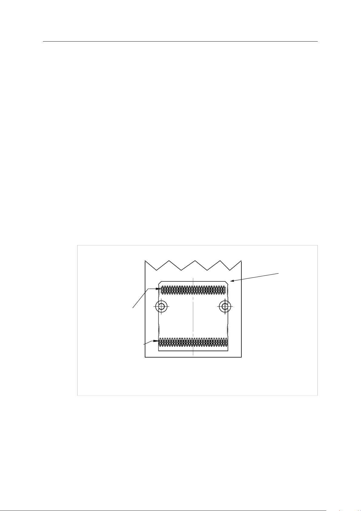
4.1 Host Application Interface
The host application connector provides an interface between the host application and the
Anybus CompactCom B40 Modbus Serial.
Anybus®CompactCom™B40 Modbus Serial User Manual
Fig. 2
The connector is implemented by a standard 1.27 mm 56 pin header surface mounted to the
bottom side of the PCB.
SCM-1202-130 1.1 en-US
Page 16

Hardware Design 14 (48)
1
2
56
55
Top view
GND 2 1 3V3
INPUT1_0 4
3 RESET
INPUT1_2 6
5 INPUT1_1
GND 8
7 INPUT1_3
INPUT1_5 10
9 INPUT1_4
INPUT1_7 12
11 INPUT1_6
GND 14
13
16
15
GND 18
17
20
19
INPUT2_6 22
21 INPUT2_7
GND 24
23 INPUT2_5
INPUT2_3 26
25 INPUT2_4
GND 28
27 INPUT2_2
MD0 30
29 INPUT2_1
OM0 32
31 INPUT2_0
GND 34
33 OM1
36
35 OM2
DE 38
37
GND 40
39
42
41
GND 44
43
46
45
48
47
GND 50
49
TX/OM3 52
51 RX
MI0 54
53 MI1
GND 56
55 3V3
Fig. 3
The picture shows the pinning of the mating connector on the host application as seen from the
top.
Anybus®CompactCom™B40 Modbus Serial User Manual
Fig. 4
See Pin Overview, p. 15 for information on how each pin is used.
SCM-1202-130 1.1 en-US
Page 17

Hardware Design 15 (48)
4.1.1 Pin Overview
Presented below is an overview of all pins except GND and 3V3.
The pin types of the connector are defined in Pin Types, p. 4. The pin type may be different
depending on which mode is used.
The pin numbers of the Anybus CompactCom B40 (brick) host application connector are
different from those of the Anybus CompactCom M40 (module) host application
connector.
Pin
Signal
Name
4 INPUT1_0 I
5 INPUT1_1 I
6 INPUT1_2 I
7 INPUT1_3 I
9 INPUT1_4 I
10 INPUT1_5 I
11 INPUT1_6 I
12 INPUT1_7 I
13
(not used)
15 I
16 O, I
17
(not used)
19 I
20
(not used)
31 INPUT2_0 I
29 INPUT2_1 I
27 INPUT2_2 I
26 INPUT2_3 I
25 INPUT2_4 I
23 INPUT2_5 I
22 INPUT2_6 I
21 INPUT2_7 I
49
(not used)
48 O
47 O
46 O
45 O
43 O
42 O
41 O
37
(not used)
39 I
36 I
38 DE O
Type Notes
I
I
O
O
I
These inputs are used to set the Modbus address of the Anybus CompactCom
See Communication Settings, p. 19
The signals can also be used to connect a DIP switch, see IO Expansion Mechanism, p.
29.
Connect directly to GND
Connect directly to 3V3
Leave unconnected
These inputs are used to set baud rate, stop bits, and parity of the Anybus
CompactCom
See Communication Settings, p. 19
The signals can also be used to connect a DIP switch, see IO Expansion Mechanism, p.
29.
Leave unconnected
Connect directly to 3V3
Active high Data Enable for RS485 transceiver
See DE (Data Enable), p. 17
®
Anybus
CompactCom™B40 Modbus Serial User Manual
SCM-1202-130 1.1 en-US
Page 18

Hardware Design 16 (48)
Pin Signal
Name
51 RX I
52
TX / OM3 I/O
32 OM0 I
33 OM1 I
35 OM2 I
54 MI0 O
53 MI1 O
30 MD0 O
3 RESET I
Type Notes
Receive Input for Modbus communication
• Direction: Host application -> Anybus CompactCom
• Idle state = High
Transmit Output for Modbus communication
• Direction: Anybus CompactCom -> Host application
• Idle state = High
This pin doubles as OM3 strapping input on Anybus CompactCom. Connect a pulldown resistor on the application for this pin in Modbus serial mode. The pull-down
resistor shall have a value between 1 kΩand 2.2 kΩ.
Set [OM2, OM1, OM0] to [0,1,1]
For more information see Settings , p. 17.
Low at power-up and before reset release.
See Settings , p. 17
Please not that this pin can be used as SYNC pin PROFINET. Used at conformance
testing.
Tied to 3V
See Settings , p. 17
Tied to GND
See Settings , p. 17
See RESET (Reset Input), p. 18
4.1.2 Power Supply Pins
Signal
GND Power 2, 8, 14, 18, 24,
3V3 Power 1, 55
Type
Pin Description
28, 34, 40, 44,
50, 56
Ground
Power and signal ground reference.
3.3 V power supply.
Anybus®CompactCom™B40 Modbus Serial User Manual
SCM-1202-130 1.1 en-US
Page 19

Hardware Design 17 (48)
4.1.3 Settings
Signal Name
OM3
OM2
OM1
OM0
MI0
MI1
MD0 O 30
RX
TX
Type
I
I
I
I
O
O
I
O
Module Detection
This signal is internally connected to GND, and can be used by the host application to detect
whether a module is present or not. When connecting an external pull-up resistor, a low signal
indicates that a module is present.
If not used, leave this signal unconnected.
4.1.4 DE (Data Enable)
Pin Description
52
35
33
32
54
53
51
52
Set [OM3, OM2, OM1, OM0] to [0,0,1,1] for Modbus Serial
operation.
OM3 is used to set operation mode at startup, and requires a
pull-down resistor. It is used as TX output after startup. The pulldown resistor shall have a value between 1 kΩand 2.2 kΩ.
[MI1, MI0] = [1,0] indicates that the Anybus CompactCom
connected comes from the Anybus CompactCom 40-series..
Module Detection
This signal can be used by the host application to determine that
an Anybus CompactCom is inserted into the slot, see Module
Detection, p. 17.
The signal is connected directly to GND on the Anybus
CompactCom.
Serial Communications Signals, used for Modbus Communication.
TX is used as OM3 during setup
The Anybus CompactCom B40 Modbus Serial supports RS485. This signal is then used as an
active high data enable signal for RS485 transceivers.
Signal Name Pin Type Pin Description
DE O 38
Data Enable
Active high signal used for RS485 transceiver.
This signal must be pulled to GND on the host application side to prevent spurious transmissions
during startup.
Anybus®CompactCom™B40 Modbus Serial User Manual
SCM-1202-130 1.1 en-US
Page 20

Hardware Design 18 (48)
Power
/RESET
0V
3.3V
Power
On
Power
Stable
t
B
t
A
V
IL
V
IH
t
t
RESET
t
C
V
IL
V
IH
t
4.1.5 RESET (Reset Input)
Signal Name Pin Type Pin Description
RESET I 3 Reset
The Anybus CompactCom does not feature any internal reset regulation. To establish a reliable
interface, the host application is solely responsible for resetting the Anybus CompactCom when
the supply voltage is out of the specified range.
Power Up
Used to reset the module.
Fig. 5
Powerup time limits are given in the table below:
Symbol
t
A
t
B
Min.
- -
1 ms
Max.
-
Definition
Time until the power supply is stable after power-on; the duration depends
on the power supply design of the host application and is thus beyond the
scope of this document.
Safety margin.
Restart
The reset pulse duration must be at least 10 µs in order for the Anybus CompactCom to properly
recognize a reset.
Fig. 6
Symbol
t
C
Min.
10 µs
Max.
-
Definition
Reset pulse width.
Anybus®CompactCom™B40 Modbus Serial User Manual
SCM-1202-130 1.1 en-US
Page 21

Hardware Design 19 (48)
4.1.6 Communication Settings
The communication settings are configured by the INPUT1 and INPUT2 input pins in the
application interface. Invalid settings results in the Anybus CompactCom entering the state
EXCEPTION.
The Modbus address is configured using INPUT1. Valid range is 1 - 247.
Baud rate, stop bits, and parity are configured using INPUT2, as defined in the tables below.
INPUT2 bits 1..0 value Stop bits, Parity
0 1, Even
1
2 2, None
3 1, None
INPUT2 bits 7..2 value Baud rate
0 - 2
3 9600
4 19200
5 38400
6 57600
7
8 115200
9 625000
10 - 64
1, Odd
(reserved)
(reserved)
(reserved)
®
Anybus
CompactCom™B40 Modbus Serial User Manual
SCM-1202-130 1.1 en-US
Page 22

Hardware Design 20 (48)
3V3
3V3
INPUT1_2
INPUT1_5
INPUT1_1
INPUT1_0
INPUT1_3
INPUT1_4
INPUT1_7
INPUT1_6
INPUT2_2
INPUT2_5
INPUT2_1
INPUT2_0
INPUT2_3
INPUT2_4
INPUT2_7
INPUT2_6
Modbus address setting = 1
Modbus baud rate setting = 4 (19200)
Modbus stop bit setting = 0 (1 stop bit, even)
Example
The figure shows INPUT1 and INPUT2 signals directly for Modbus communication. INPUT1 signals
are strapped to Modbus address 0x01. INPUT2 signals are set to configure 1 stop bit, even parity
and baud rate 19200.
Fig. 7
®
Anybus
CompactCom™B40 Modbus Serial User Manual
SCM-1202-130 1.1 en-US
Page 23

Hardware Design 21 (48)
Pin 1
Application
interface
Pin 1
Network
interface
Outline of brick
Top view
1
2
52
51
Top view
4.2 Network Connector
The network connector provides network access to the Anybus CompactCom B40 Modbus Serial.
Fig. 8
The signals from the network connector can be directly routed to the (optional) connector board,
which carries a network connector(s) identical or similar to the ones on the corresponding
Anybus CompactCom M40 module.
Examples on how to design the network access circuitry, when not using the connector board,
are shown in Network Interface Examples, p. 47.
The brick has a standard 1.27 mm 52 pin header surface mounted to the bottom side of the
board as network interface.
Anybus®CompactCom™B40 Modbus Serial User Manual
Fig. 9
The pictures shows the pinning of the corresponding network connector on the host application
board, seen from the top.
SCM-1202-130 1.1 en-US
Page 24

Hardware Design 22 (48)
GND 2 1 3V3
B_1CEN/SDA 4
3 B_1P/RXP
GND 6
5 B_1N/RXN
B_2CEN/SCL 8
7 B_2P/SDP
GND 10
9 B_2N/SDN
B_3CEN 12
11 B_3P/TXEN
GND 14
13 B_3N/TXDIS
B_4CEN/BUSP 16
15 B_4P/TXP
GND 18
17 B_4N/TXN
NW_LED4A 20
19 NW_LED4B
NW_LED3A 22
21 NW_LED3B
NW_LED2A 24
23 NW_LED2B
NW_LED1A 26
25 NW_LED1B
GND 28
27 3V3
A_1CEN/SDA 30
29 A_1P/RXP
GND 32
31 A_1N/RXN
A_2CEN/SCL 34
33 A_2P/SDP
GND 36
35 A_2N/SDN
A_3CEN 38
37 A_3P/TXEN
GND 40
39 A_3N/TXDIS
A_4CEN/BUSP 42
41 A_4P/TXP
GND 44
43 A_4N/TXN
C_RX 46
45 C_TX
C_BUSP 48
47 C_TXEN
GATE2 50
49 GATE1
GND 52
51 3V3
Fig. 10
4.2.1 Overview
Depending on network, the pins have different names and different functionalities. Presented
below is an overview of all pins except GND and 3V3. More detailed descriptions of the signals
are described for each available network/fieldbus version later in this section (4.2). Please note
that at the moment only EtherNet/IP and PROFINET IRT are available.
Anybus®CompactCom™B40 Modbus Serial User Manual
SCM-1202-130 1.1 en-US
Page 25

Hardware Design 23 (48)
Pin Signal Name
Ethernet based
networks, Copper
3 B_1P B_RXP
4 B_1CEN B_SDA
5 B_1N B_RXN
7 B_2P B_SDP
8 B_2CEN B_SCL
9 B_2N B_SDN
11 B_3P B_TXEN
12 B_3CEN
13 B_3N B_XDIS
15 B_4P B_TXP
16 B_4CEN
17 B_4N B_TXN
19 NW_LED4B NW_LED4B NW_LED4B NW_LED4B NW_LED4B
20 NW_LED4A NW_LED4A NW_LED4A NW_LED4A NW_LED4A
21 NW_LED3B NW_LED3B NW_LED3B NW_LED3B NW_LED3B
22 NW_LED3A NW_LED3A NW_LED3A NW_LED3A NW_LED3A
23 NW_LED2B NW_LED2B NW_LED2B NW_LED2B NW_LED2B
24 NW_LED2A NW_LED2A NW_LED2A NW_LED2A NW_LED2A
25 NW_LED1B NW_LED1B NW_LED1B NW_LED1B NW_LED1B
26 NW_LED1A NW_LED1A NW_LED1A NW_LED1A NW_LED1A
29 A_1P A_RXP
30 A_1CEN A_SDA
31 A_1N A_RXN
33 A_2P A_SDP
34 A_2CEN A_SCL
35 A_2N A_SDN
37 A_3P A_TXEN
38 A_3CEN
39 A_3N A_TXDIS
41 A_4P A_TXP
42 A_4CEN
43 A_4N A_TXN
45 C_TX C_TX C_TX
46 C_RX C_RX C_RX
47 C_TXEN C_TXEN
48 C_BUSP_N
49 GATE1 GATE1 GATE1
50 GATE2 GATE2 GATE2
Ethernet based
networks, fiber optic
DeviceNet
PROFIBUS
CC-Link
At the moment the following copper wired Ethernet protocols are available: EtherNet/IP and
PROFINET IRT. The speed of all these protocols is 100 Mb/s (using signal pairs 1-2 of each port).
PROFINET IRT is also available for fiber optic.
The LED signals are active high and should be connected to the respective LEDs via a resistor.
The pin types of the connector are defined in Pin Types, p. 4. The pin types are specified for each
network type on the following pages.
Anybus®CompactCom™B40 Modbus Serial User Manual
SCM-1202-130 1.1 en-US
Page 26

Hardware Design 24 (48)
4.2.2 Power Supply Pins
Signal Name
GND Power 2, 6, 10,
3V3 Power 1, 27, 51
Type
Pin No. Description
14, 18, 28,
32, 36, 40,
44, 52
Ground
Power and signal ground reference.
3.3 V power supply.
4.2.3 How to Connect Unused Network Connector Pins
For Ethernet versions of the Anybus CompactCom B40 Modbus Serial it is recommended to
terminate Ethernet signals in the network interface if one of the Ethernet ports is unused. For
the 10/100 Mb/s hardware version it is sufficient to terminate pair no. 1 and 2, for the port of
concern, while for the 1 Gb/s hardware version this has to be done for pair no. 1, 2, 3, and 4.
Fig. 11
Unused fibre optic connector pins should be connected as follows:
• 100R between TXP and TXN
• 820R between SDN and 3V3, resulting in 2 V on SDN
• 1k5 between SDP and 3V3, resulting in 1.5 V on SDP- Indicates that no signal is received. A
signal amplitude of 0.5 V is appropriate.
• 4k7 between SCL and 3V3
• 4k7 between SDA and 3V3
Other network signals may be left floating when not used.
Anybus®CompactCom™B40 Modbus Serial User Manual
SCM-1202-130 1.1 en-US
Page 27

Hardware Design 25 (48)
4.2.4 Ethernet Based Networks (Copper)
The industrial networks, that use Ethernet for communication, share the same hardware design.
However, the firmware downloaded to the brick is different depending on network. Physically
they use the same set of pins in a similar way. At the moment Anybus CompactCom B40 Modbus
Serial is available for the following Ethernet based networks: EtherNet/IP and PROFINET IRT.
The brick supports dual network ports, signal group A should be connected to the left port (port
1) and signal group B to the right port (port 2) on the connector board, looking at the front, see
Connector Board for Copper Based Ethernet, p. 35
Signal Group Signal Name Type
B B_1P
B_1CEN Power 4
B_1N
B_2P
B_2CEN Power 8
B_2N
B_3P
B_3CEN Power 12
B_3N
B_4P
B_4CEN Power 16
B_4N
A A_1P
A_1CEN Power 30
A_1N
A_2P
A_2CEN Power 34
A_2N
A_3P
A_3CEN Power 38
A_3N
A_4P
A_4CEN Power 42
A_4N
I/O
I/O
I/O
I/O
I/O
I/O
I/O
I/O
I/O
I/O
I/O
I/O
I/O
I/O
I/O
I/O
Pin
3
5
7
9
11
13
15
17
29
31
33
35
37
39
41
43
Description
First pair, positive signal
Center tap voltage for first pair
First pair, negative signal
Second pair, positive signal
Center tap voltage for second pair
Second pair, negative signal
Third pair, positive signal. Used for Gigabit Ethernet.
Center tap voltage for third pair. Used for Gigabit
Ethernet.
Third pair, negative signal. Used for Gigabit Ethernet.
Fourth pair, positive signal. Used for Gigabit Ethernet.
Center tap voltage for fourth pair. Used for Gigabit
Ethernet.
Forth pair, negative signal. Used for Gigabit Ethernet.
4.2.5 Ethernet Fiber Optic Networks
Ethernet fiber optic networks use more or less the same pins as copper based Ethernet networks.
The brick supports PROFINET fiber optic network (PROFINET IRT).
The brick supports dual network ports, signal group A is be connected to the left port (port 1)
and signal group B to the right port (port 2)on the connector board, looking at the front, see
Fiber Optic Conenctor LÄNK!!.
If the Anybus CompactCom B40 connector board is not to be used, please study the design
requirements for the Rx and SD channels, see Rx Channel Design Requirements, p. 26 and SD
Channel Design Requirements, p. 27. Furthermore, fiber optic connectors without metal are
preferred in order to minimize EMC disturbance.
Anybus®CompactCom™B40 Modbus Serial User Manual
SCM-1202-130 1.1 en-US
Page 28

Hardware Design 26 (48)
Brick
Trans-
ceiver
Trans-
ceiver
Trans-
ceiver
Brick Brick
AC coupled transceiver DC coupled transceiver DC coupled transceiver with bias current
Signal Group Signal Name
B B_RXP I 3
B_SDA
B_RXN I 5
B_SDP I 7
B_SCL
B_SDN I 9
B_TXEN O 11
B_TXDIS O 13
B_TXP O 15
B_TXN O 17
A A_RXP I 29
A_SDA
A_RXN I 31
A_SDP I 33
A_SCL
A_SDN I 35
A_TXEN O 37
A_TXDIS O 39
A_TXP O 41
A_TXN O 43
Type
I/O
I/O
I/O
I/O
Pin Description
4
8
30
34
Rx, LVPECL positive signal
SDA, I2C data
Rx, LVPECL negative signal
Signal Detect, LVPECL positive signal
SCL, I2C clock
Signal Detect, LVPECL negative signal
Tx enable
TXEN is implemented as the inverse to TXDIS
Tx disable
Tx, LVPECL positive signal
Tx, LVPECL negative signal
Rx, LVPECL positive signal
SDA, I2C data
Rx, LVPECL negative signal
Signal Detect, LVPECL positive signal
SCL, I2C clock
Signal Detect, LVPECL negative signal
Tx enable
TXEN is implemented as the inverse to TXDIS
Tx disable
Tx, LVPECL positive signal
Tx, LVPECL negative signal
The differential signals Rx and Tx should be routed as differential pairs with a characteristic
impedance of 100 Ω differentially.
Rx Channel Design Requirements
The Rx channel is designed for an optical transceiver output that has an AC coupled 100 Ω
differential signal with 100-1000 mV amplitude, e.g. LVPECL (low voltage positive emitter
coupled logic). Each line is terminated with 50 Ω to a common point with a potential of 1.2 V on
the brick.
If a transceiver with a DC coupled output is used, series capacitors are needed to obtain desired
signal levels for the brick. Below is a figure describing three different options to connect a
transceiver output to an Rx channel on the brick:
Fig. 12
The AC coupling capacitors typically have a value of 100 nF. Resistors draining bias current
typically have a value of 150 Ω.
Anybus®CompactCom™B40 Modbus Serial User Manual
SCM-1202-130 1.1 en-US
Page 29

Hardware Design 27 (48)
Brick
Trans-
ceiver
Trans-
ceiver
Trans-
ceiver
Brick Brick
a: Differential
LVPECL output
b: Single ended LVPECL output
If the output is active low:
Connect the output to SDN and
the 820 Ω resistor to SDP .
c: LVCMOS output. If the output is
active low, connect the 1.8 kΩ
resistor to SDN instead.
SD Channel Design Requirements
The SD (signal detect) channel is designed for a transceiver output that has a DC coupled
differential output with 100-1000 mV amplitude. If a transceiver with LVTTL/LVCMOS output is
used, the signal needs to be conditioned using a few resistors, to obtain desired signal levels for
the brick.
Each line is pulled to GND by a 1.27 kΩ resistor on the brick.
Even if the transceiver has a single ended output and the other line is at a fixed reference
potential, it is recommended to route SDN and SDP side by side all the way to the signal
conditioning resistors. This will give the interference, collected by the transmission line, common
mode characteristics, and it can thus be ignored by the differential input, instead of becoming a
differential mode interference that would corrupt the signal.
Below is a figure describing three different ways to connect a transceiver output to an SD
channel of the brick:
Fig. 13
In case a and case b, additional pull-down resistors will be required if the LVPECL outputs require
a certain bias current (> 1 mA) to function.
Anybus®CompactCom™B40 Modbus Serial User Manual
SCM-1202-130 1.1 en-US
Page 30

Hardware Design 28 (48)
Brick
network
interface
G
Y
220 Ω
220 Ω
NW_LED4A
NW_LED4B
4.2.6 LED Indicators
The Anybus CompactCom 40 series supports four bicolored LED indicators.
LED name Pin no.
LED1 26 NW_LED1A Green
25 NW_LED1B
LED2 24 NW_LED2A Green
23 NW_LED2B
LED3 22 NW_LED3A Green
21 NW_LED3B
LED4 20 NW_LED4A Green
19 NW_LED4B
Signal Name
Default color
Red
Red
Yellow
Yellow
Default Functionality
Network status
Module status
All Industrial
Ethernet Networks:
Other: Not used
EtherNet/IP, Modbus
TCP
Other Not used
All Industrial
Ethernet Networks:
Other: Not used
EtherNet/IP, Modbus
TCP
Other Not used
Link/Act for the
network port (port A)
10 Mbit Link/Act for
Link/Act for the
network port (port A)
Link/Act for the
network port (port B)
10 Mbit Link/Act for
Link/Act for the
network port (port B)
All LED outputs are active high and should be connected as shown in the picture below. The
resistor values should be chosen to get even light between different LEDs.
Fig. 14
4.3 Network Configuration Switches
Modbus registers 0x5200 (Application switch 1) and 0x5201 (Application switch 2) can be used
for network configuration. Application switch 1 is generally used to configure the node address
and application switch 2 to configure the network baud rate.
It is recommended to provide means for the end user to set the values of these registers, using
physical switches like DIP switches, rotaries etc. The application is responsible for reading the
switch values and then writing them to Modbus registers 0x5200 (Application switch 1) and
0x5201 (Application switch 2).
If the application processor does not have sufficient input pins to connect physical switches,
there is a mechanism for I/O expansion that can be used. The switches are then connected to
the Anybus CompactCom B40 Modbus Serial instead. For more information see IO Expansion
Mechanism, p. 29.
Please refer to the applicable network appendix for a description of the contents of the registers.
Anybus®CompactCom™B40 Modbus Serial User Manual
SCM-1202-130 1.1 en-US
Page 31

Hardware Design 29 (48)
4.4 IO Expansion Mechanism
If the application is to implement physical switches for network configuration, but does not have
sufficient I/O pins, the switches can be connected to the Anybus CompactCom instead using the
IO Expansion Mechanism. The INPUT1 and INPUT2 pins can then be used both to strap the
Modbus communication settings and to connect the physical switches.
The Anybus CompactCom will sample the INPUT1 and INPUT2 pins to determine the Modbus
communication settings before Modbus communication is performed. When the first Modbus
telegram has been exchanged, the DE signal can be used to alter the INPUT1 and INPUT2 signals
to sample the physical switches. The application processor can then read the INPUT1 and INPUT2
pins in Modbus register 0x0FFD (Anybus switch status) and write back the values to Modbus
registers 0x5200 (Application switch 1) and 0x5201 (Application switch 2).
Anybus®CompactCom™B40 Modbus Serial User Manual
SCM-1202-130 1.1 en-US
Page 32

Hardware Design 30 (48)
INPUT1_2
INPUT1_5
INPUT1_1
INPUT1_0
INPUT1_3
INPUT1_4
INPUT1_7
INPUT1_6
INPUT2_2
INPUT2_5
INPUT2_1
INPUT2_0
INPUT2_3
INPUT2_4
INPUT2_7
INPUT2_6
Modbus baud rate setting = 4 (19200)
Modbus stop bit setting = 0 (1 stop bit, even)
3V3
3V3
3V3
3V3
SW DIP-8
SW DIP-8
Network address
Network baud rate, stop bits and parity
DE
nReset
CLK
CLR
PRE
D
Q
Q
74LVC74
Modbus address setting = 1
Fig. 15
Anybus
®
CompactCom™B40 Modbus Serial User Manual
SCM-1202-130 1.1 en-US
Page 33

Appendix A: Technical Specification 31 (48)
A Technical Specification
A.1 Environmental
A.1.1 Operating
-40 to 85° C (-40 to 185° F)
A.1.2 Storage
-40 to 85°C (-40 to 185° F)
A.1.3 Humidity
5 to 95% non-condensing
A.2 Shock and Vibration
A.2.1 Shock
The Anybus CompactCom B40 Modbus Serial is tested according to IEC 68–2–27
• half-sine 30 g, 11 ms, 3 positive and 3 negative shocks in each of three mutually
perpendicular directions
• half-sine 50 g, 11 ms, 3 positive and 3 negative shocks in each of three mutually
perpendicular directions
Connector boards/interface cards are tested for 30 g.
A.2.2 Sinusoidal Vibration
The Anybus CompactCom B40 Modbus Serial is tested according to IEC 68–2–6
Frequency range: 10–500 Hz
Amplitude 10–49 Hz:
Acceleration 50–500 Hz
Sweep rate:
0.35 mm
5 g
1 oct/min
10 double sweep in each of the three mutually perpendicular directions
A.3 Electrical Characteristics
Failure to follow the requirements may lead to permanent hardware damage
It is recommended for Anybus CompactCom B40 Modbus Serial users to make sure that each
signal controlling the Anybus CompactCom B40 Modbus Serial has a drive strength enough to
fulfill level and timing constraints even if the signal is loaded with 20 pF in parallel with 2.2 kΩ to
GND or 3V3.
Anybus®CompactCom™B40 Modbus Serial User Manual
SCM-1202-130 1.1 en-US
Page 34

Appendix A: Technical Specification 32 (48)
A.3.1 Operating Conditions
Symbol
3V3
GND Ground reference 0.00 0.00 0.00 V
I
IN
V
IH
V
IL
I
OH
I
OL
V
OH
V
OL
I
OH
(NW_
LEDx)
Parameter
Supply Voltage (DC)
Ripple (AC)
Current consumption
(also including network
interfaces and network
status LEDs)
Input High Voltage
Input Low Voltage
Current, Output High
Current, Output Low
Output High Voltage
Output Low Voltage
Output Current ,
network LEDs
Pin
Types
PWR
I, BI
O, BI
O 20 mA
Conditions Min.
3.15 3.30 3.45 V
- - ± 100 mV
Class A - - 250 mA
Class B - - 500 mA
Class C - - 1000 mA
-
-
= -4mA 2.4
I
OH
= 4mA
I
OL
2.0
-0.3
-8.0
- -
Typ.
-
-
-
- -
Max. Unit
3.45 V
0.8 V
8.0 mA
0.4 V
I= Input, CMOS (3.3V)
O= Output, CMOS (3.3V)
BI= Bidirectional, Tristate
PWR= Power supply inputs
V
A.4 Regulatory Compliance
EMC Compliance (CE)
Since the Anybus CompactCom is considered a component for embedded applications it cannot
be CE-marked as an end product.
However the Anybus CompactCom 40 family is pre-compliance tested in a typical installation
providing that all modules are conforming to the EMC directive in this installation.
The EMC pre-testing has been conducted according to the following standards:
Emission: EN61000-6-4 EN55016-2-3 Radiated emission
EN55022 Conducted emission
Immunity: EN61000-6-2 EN61000-4-2 Electrostatic discharge
EN61000-4-3 Radiated immunity
EN61000-4-4 Fast transients/burst
EN61000-4-5 Surge immunity
EN61000-4-6 Conducted immunity
Since all Anybus CompactCom B40 Modbus Serial modules have been evaluated according to the
EMC directive through above standards, this serves as a base for our customers when certifying
Anybus CompactCom B40 Modbus Serial based products.
Anybus®CompactCom™B40 Modbus Serial User Manual
SCM-1202-130 1.1 en-US
Page 35

Appendix B: Mechanical Specification 33 (48)
36
36
33
13
2x
3,2
1,5 ± 0,25
2,3 ± 0,25
27 ± 0,20 4,5 ± 0,20
1,27 ± 0,05
1,27
2x26p
2x28p
8=max module height
Pin 1
Application
interface
Pin 1
Network
interface
Bottom view
B Mechanical Specification
This is a class A product. In a domestic environment this product may cause radio
interference in which case the user may be required to take adequate measures.
This product contains parts that can be damaged by electrostatic discharge (ESD). Use
ESD prevention measures to avoid damage.
All dimensions are in millimeters, tolerance ±0.10 mm, unless otherwise stated.
B.1 Anybus CompactCom B40 Modbus Serial
The dimensions for the Anybus CompactCom B40 Modbus Serial are given in the picture below.
Fig. 16
Anybus
®
CompactCom™B40 Modbus Serial User Manual
SCM-1202-130 1.1 en-US
Page 36

Appendix B: Mechanical Specification 34 (48)
33
2xM3
27
8,5
Pin 1
Application
interface
Pin 1
Network
interface
Outline of brick
Top view
1.5
2.3
27 4.5
8 = max module height
B.2 Footprint
The Anybus CompactCom is connected to the host application board through the host
application interface connector and a network interface connector. The footprint for the Anybus
CompactCom is shown in the picture below.
B.3 Height Restrictions
Fig. 17
All dimensions are in millimeters
Fig. 18
The maximum height occupied by onboard components of the Anybus module is 8 mm. To ensure
isolation, it is recommended to add an additional 2.5 mm on top of these dimensions.
Anybus®CompactCom™B40 Modbus Serial User Manual
SCM-1202-130 1.1 en-US
Page 37

Appendix B: Mechanical Specification 35 (48)
1,5 ± 0,25
2,3 ± 0,25
3,5 ± 0,20
2,9 12,7
37,8
15,6
40
20
18
32
35
3,2
B.4 Network Connector Boards (Optional)
B.4.1 Connector Board for Copper Based Ethernet
The connector board for the copper based Ethernet network interfaces carries two RJ45
connectors.
Fig. 19
B.5 Connector Board for Fiber Optic Ethernet
The connector board for the Fiber Optic Ethernet network interface carries two fibre optic
transceivers.
Anybus®CompactCom™B40 Modbus Serial User Manual
SCM-1202-130 1.1 en-US
Page 38

Appendix B: Mechanical Specification 36 (48)
1,5 ± 0,25
2,3 ± 0,25
3,5 ± 0,20
2,9 13,2
40,3
16,8
20
40
18
32
44,5
3,2
Fig. 20
Anybus
®
CompactCom™B40 Modbus Serial User Manual
SCM-1202-130 1.1 en-US
Page 39

Appendix B: Mechanical Specification 37 (48)
B.6 Assembly
The Anybus CompactCom B40 Modbus Serial and the connector board are mounted separately
on to the host application board. The connector board has to be secured using a screw, joining
FE (functional earth) on the connector board to FE on the host application board. The screw
holes of the Anybus CompactCom B40 Modbus Serial are not connected to FE, but to GND. If
suggested components are used, the Anybus CompactCom B40 Modbus Serial can be mounted
without screws in a low vibration environment, see Shock and Vibration, p. 31 for more
information.
The Anybus CompactCom B40 Modbus Serial can either be connected to the application board
using headers, or soldered directly to the host application PCB.
Fig. 21
Suggested components
Header Application interface Samtec CLP-128-02-L-D (56 pin)
Network interface Samtec CLP-126-02-L-D (52 pin)
Stand-off (M3)
Pemnet SMTSO-M3-4-ET
The screw standoffs are typically 4 mm tall. If the Anybus CompactCom B40 Modbus Serial and
connector board are to be soldered directly to the host application board, standoffs should be 2
mm tall. Outer diameter may be 6 mm max. The standoffs should not extend outside the screw
mount pads.
Recommended torque is 0.2 Nm. Locking paint can be used to secure the screws against
loosening.
Anybus®CompactCom™B40 Modbus Serial User Manual
SCM-1202-130 1.1 en-US
Page 40

Appendix B: Mechanical Specification 38 (48)
33
2xM3
M3
27
8,5 14,5
Pin 1
Application
interface
Pin 1
Network
interface
Pin 1
Network
interface
PCB layout
Standoffs, typ. 4 mm
FE
Outline of brick
Outline of
connector board
M3: Standoff with internal thread, size M3
Top view
Top view
Fig. 22
®
Anybus
CompactCom™B40 Modbus Serial User Manual
SCM-1202-130 1.1 en-US
Page 41

Appendix C: Firmware Upgrade 39 (48)
C Firmware Upgrade
Download and upgrade of network communication firmware for a specific fieldbus or industrial
network can be performed in different ways, depending on which Anybus CompactCom B40
Modbus Serial that is to be upgraded.
Ethernet versions with FTP
enabled
Ethernet versions with FTP
disabled
Fieldbus versions
Use the Firmware Manager II tool or download the firmware to the designated folder in
the file system.
Unplug the Anybus CompactCom from the host application pcb and use the Anybus
CompactCom 40 Starter Kit to perform the firmware upgrade. See the starter kit
documentation for further information.
®
Anybus
CompactCom™B40 Modbus Serial User Manual
SCM-1202-130 1.1 en-US
Page 42

Appendix C: Firmware Upgrade 40 (48)
C.1 Using Firmware Manager II
This tool is available without cost from www.anybus.com and can be downloaded from the
product pages. It can be used to download new firmware for any Ethernet Anybus CompactCom
B40 Modbus Serial. Please note that FTP has to be enabled.
Fig. 23
Using the tool, perform the following steps to download new firmware to the module.
1. Connect a computer with the Firmware Manager II software installed to the network
containing the module.
2. Start the Firmware Manager II tool.
3. Scan the network and find the module.
4. Click the Firmware Repository icon in the menu, to open the Firmware Repository window.
Drag the firmware folder into the window to add the new firmware to the repository. Close
the Firmware Repository window.
5. In the scan window, under the “Available Networks” tab, select the appropriate firmware
for the module. Click the Change Network button. A confirmation window will appear. Click
Yes to start the download of the new firmware. Please make sure that download is
completely finished before continuing.
6. After download, a restart of the module is needed to install the new firmware. If the
application allows it, it is possible to restart the module via the Restart Module button in
the Firmware Manager II tool. If the application does not allow restart from the network, a
manual restart of the module is needed.
For more information, see the help file in the Firmware Manager II software.
Anybus®CompactCom™B40 Modbus Serial User Manual
SCM-1202-130 1.1 en-US
Page 43

Appendix C: Firmware Upgrade 41 (48)
C.2 Using FTP
If the module supports FTP, this can be used to access the file system and upload the new
firmware directly to the /firmware directory. The next time the module is started the firmware
will be upgraded. After the firmware is installed, the firmware file is deleted from the /firmware
directory.
Anybus®CompactCom™B40 Modbus Serial User Manual
SCM-1202-130 1.1 en-US
Page 44

Appendix D: The Anybus State Machine 42 (48)
SETUP
(00h)
WAIT_PROCESS
(02h)
PROCESS_ACTIVE
(04h)
IDLE
(03h)
EXCEPTION
(07h)
(Power up)
(From all states)
ERROR
(05h)
NW_INIT
(01h)
D The Anybus State Machine
D.1 General Information
A fundamental part of the Anybus CompactCom B40 Modbus Serial is the Anybus State Machine.
The state machine shall be regarded as a Moore machine; i.e. the host application is not required
to keep track of all state transitions, however it is expected to perform certain tasks in each state
Fig. 24
®
Anybus
CompactCom™B40 Modbus Serial User Manual
SCM-1202-130 1.1 en-US
Page 45

Appendix D: The Anybus State Machine 43 (48)
D.2 State Dependent Actions
The expected actions for each state are listed below.
State
SETUP
NW_INIT
WAIT_PROCESS
IDLE
PROCESS_ACTIVE
ERROR
EXCEPTION
The host application must keep the Write Process Data updated in NW_INIT (initial data),
WAIT_PROCESS, IDLE, ERROR and PROCESS_ACTIVE since this data is buffered by the
Anybus CompactCom, and may be sent to the network after a state shift.
Description Expected Actions
Anybus CompactCom Setup in progress.
The Anybus CompactCom module is currently performing
network-related initialization tasks.
The network Process Data channel is temporarily inactive. The host application shall
The network interface is idle. The exact interpretation of this
state is network specific. Depending on the configuration in
the offline action register, the Read Process Data may be either
updated or static (unchanged), unless “offline action” is set to
“clear”, in which case the Read Process Data is cleared in this
state.
Normal data handling is possible Perform normal data
There is at least one serious network error.
The module has ceased all network participation due to a host
application related error.
This state is unrecoverable, i.e. the module must be restarted
in order to be able to exchange network data.
regard the Read Process
Data as not valid.
The host application may
act upon the Read Process
Data, or go to an idle state.
handling.
Anybus®CompactCom™B40 Modbus Serial User Manual
SCM-1202-130 1.1 en-US
Page 46

Appendix E: Implementation Guidelines 44 (48)
Host Application
CPU (3.3V)
3V3
3V3
3V3
OM0
OM1
OM2
Tx/OM3
Rx
IRQ
RESET
MI0/SYNC
MI1
MD
Rx
Tx
GPIO5
GPIO6
GPIO7
GPIO8
GPIO10
INPUT2_0
INPUT2_1
INPUT2_2
INPUT2_3
INPUT2_4
INPUT2_5
INPUT2_6
INPUT2_7
3V3 3V3
INPUT1_0
INPUT1_1
INPUT1_2
INPUT1_3
INPUT1_4
INPUT1_5
INPUT1_6
INPUT1_7
Modbus address,
either strapped
or from switch
Number of stop bits,
parity and baud rate
strapped
or from switch
E Implementation Guidelines
E.1 General
This appendix provides an example of a possible implementation for the Anybus CompactCom
B40 Modbus Serial.
There are many different processors with different functionality available on the market today.
The implementation in this appendix is to be regarded as an example that is designed for one
single type of processor. Other hardware interfaces may require adjustments for timing, different
functionality etc. It is important to fully understand the interface to take correct design decisions
in order to obtain a stable and reliable design.
E.2 Example
The example in the figure below shows an implementation with Modbus Serial communication.
Anybus
Fig. 25
®
CompactCom™B40 Modbus Serial User Manual
SCM-1202-130 1.1 en-US
Page 47

Appendix E: Implementation Guidelines 45 (48)
E.3 Power Supply Considerations
E.3.1 General
The Anybus CompactCom 40 platform in itself is designed to be extremely power efficient. The
exact power requirements for a particular networking system will however vary a lot depending
on the components used in the actual bus circuitry.
While some systems usually require less than 250 mA of supply current at 3.3 V, some high
performance networks, or networks which require the use of legacy ASIC technology, will
consume up to 500 mA, or in rare cases even as much as 1000 mA.
As an aid when designing the power supply electronics, the networks have been divided into
classes based on their power consumption as follows.
• Class A: less than 250 mA
• Class B: up to 500 mA
• Class C: up to 1000 mA
Please note that the power supply classifications take into account that the power budget is
shared with a full fieldbus circuitry, e.g. the appropriate connector board and NW_LEDs with
maximized consumption (20 mA each).
The following table lists the currently supported networking systems and their corresponding
class.
Network Class A Class B Class C
DeviceNet X
PROFIBUS X
CANopen X
EtherCAT
PROFINET 2-Port X
PROFINET FO 2-Port X
Ethernet/IP 2-Port
EtherNet POWERLINK
Common Ethernet
CC-Link
Modbus-TCP 2-Port
CC-Link IE Field
BACnet/IP
X
X
X
X
X
X
X
X
A power supply designed to fulfill Class A requirements (250 mA), will be able to support all
networks belonging to class A, but none of the networks in Class B and C.
A power supply designed to fulfill Class C requirements, will be able to support all networks.
Anybus®CompactCom™B40 Modbus Serial User Manual
SCM-1202-130 1.1 en-US
Page 48

Appendix E: Implementation Guidelines 46 (48)
3V3
GND
C1
3.3 V
GND
5V
SS14
BAV70
22uF
(6.3V)
4k7
LT1767
10uH
100nF
(16V)
100nF
(16V)
1,5nF
(50V)
10uF
(6.3V)
Vin
FB
Vsw
GND
Vc
SHDN
SYNC
BOOST
VDD (3.3V)
GND
C1
C2
E.3.2 Bypass Capacitance
The power supply inputs must have adequate bypass capacitance for high-frequency noise
suppression. It is therefore recommended to add extra bulk capacitors near preferably all the
power supply inputs (or at least two):
Reference
C1
Fig. 26
E.3.3 3.3 V Regulation
The following example uses the LT1767 from Linear Technology to provide a stable 3.3 V power
source for the module. Note that all capacitors in this example are of ceramic type.
Value (Ceramic)
10 µF / 6.3 V
Fig. 27
For detailed information regarding this example, consult the data sheet for the LT1767 (Linear
Technology).
Anybus®CompactCom™B40 Modbus Serial User Manual
SCM-1202-130 1.1 en-US
Page 49

Appendix F: Network Interface Examples 47 (48)
F Network Interface Examples
This section offers a typical example of how to design the network interface.
Anybus®CompactCom™B40 Modbus Serial User Manual
SCM-1202-130 1.1 en-US
Page 50

5
4
3
2
1
Design Example
10 and 100 Mbit Ethernet
Network Interface
with RJ-45 connectors
D D
TR2
J6
1
2
3
4
5
6
7
8
9
10
11
12
13
14
15
16
17
18
C C
19
20
21
22
23
24
25
26
3V3
B_1P/RXP
B_1CEN/SDA
B_1N/RXN
B_2P/SDP
B_2N/SDN
B_3P/TXEN
B_3CEN/RX
B_3N/TXDIS
B_4P/TXP/TX
B_4CEN/CD/BUSP_N
B_4N/TXN/TX_N
NW_LED4B_N
NW_LED4A_N
NW_LED3B_N
NW_LED3A_N
NW_LED2B_N
NW_LED2A_N
NW_LED1B_N
NW_LED1A_N
B_1P
B_1N
B_1CEN
B_2CENB_2CEN/SCL
B_2P
B_2N
1 2
C2
100nF/16V
Ethernet Trafo
7490100111A (Würth Elektronik Gmbh)
C3
100nF/16V
TDB+ TDB+
TDB-
TDBRDB+
RDB-
RDB+
SHIELDB
RDB-
R2
75R
R3
75R
C4
1nF/2kV
R4
75R
R5
75R
C1
1nF/2kV
FE
J5
1
1
2
2
3
3
4
4
5
5
6
6
7
7
8
8
9
9
10
10
RJ-45 connector
SS-60300-032 (Bel stewart)
FE
R1
1M
27
28
29
30
31
32
33
34
35
36
37
38
39
40
B B
41
42
43
44
45
46
47
48
49
50
51
52
B40-1 connector
3V3
A_1CEN/SDA
A_1N/RXN
A_2P/SDP
A_2CEN/SCL
A_2N/SDN
A_3P/TXEN
A_3CEN/RX
A_3N/TXDIS
A_4P/TXP/TX
A_4CEN/CD/BUSP_N
A_4N/TXN/TX_N
C_TX
C_RX
C_TXEN
C_BUSP_N
GATE1
GATE2
3V3
A_1PA_1P/RXP
A_1N
A_1CEN
A_2CEN
A_2P
A_2N
3 4
C6
100nF/16V
Notes:
1,2,3,4) Place center tap capacitors close to the respective
transformer.
TR1
Ethernet Trafo
7490100111A (Würth Elektronik Gmbh)
C7
100nF/16V
TDA+ TDA+
TDA-
TDARDA+
RDA-
SHIELDA
RDA+
RDA-
R8
75R
R9
75R
C8
1nF/2kV
R6
75R
R10
75R
C5
1nF/2kV
FE
J4
1
1
2
2
3
3
4
4
5
5
6
6
7
7
8
8
9
9
10
10
RJ-45 connector
SS-60300-032 (Bel stewart)
FE
R7
1M
A A
5
4
3
2
1
Page 51

5
4
3
2
1
Design Example
3V3
J1, pin #1
C1
10uF/10V
D D
C C
B B
J1
1
2
3
4
5
6
7
8
9
10
11
12
13
14
15
16
17
18
19
20
21
22
23
24
25
26
27
28
29
30
31
32
33
34
35
36
37
38
39
40
41
42
43
44
45
46
47
48
49
50
51
52
3V3
B_1P/RXP
B_1CEN/SDA
B_1N/RXN
B_2P/SDP
B_2CEN/SCL
B_2N/SDN
B_3P/TXEN
B_3CEN/RX
B_3N/TXDIS
B_4P/TXP/TX
B_4CEN/CD/BUSP_N
B_4N/TXN/TX_N B_TXN
NW_LED4B_N
NW_LED4A_N
NW_LED3B_N
NW_LED3A_N
NW_LED2B_N
NW_LED2A_N
NW_LED1B_N
NW_LED1A_N
3V3
A_1P/RXP
A_1CEN/SDA
A_1N/RXN
A_2P/SDP
A_2CEN/SCL
A_2N/SDN
A_3P/TXEN
A_3CEN/RX
A_3N/TXDIS
A_4P/TXP/TX
A_4CEN/CD/BUSP_N
A_4N/TXN/TX_N
C_TX
C_RX
C_TXEN
C_BUSP_N
GATE1
GATE2
3V3
C2
100nF/16V
B_SDN
B_SDP
B_RXN
B_RXP
B_TXP
1
B_SDA
B_SCL
B_TXDIS
A_SDA
A_SCL
A_TXDIS
A_SDN
A_SDP
A_RXN
A_RXP
A_TXP
A_TXN
1
3V3
R5
820R
3V3
R3
150R
R8
150R
R6
820R
R2
0R
2
R1
0R
2
R4
150R
R9
150R
3V3
B_SDPA
B_RXNA
B_RXPA
A_SDPA
A_RXNA
A_RXPA
2
R10
4k7
R11
4k7
C15
100nF/16V
R12
4k7
C17
100nF/16V
C16
100nF/16V
R13
4k7
C18
100nF/16V
Ethernet Fibre Optics
Network Interface
5
4
3
2
1
SD
RD-
RxVCC
RxGND
12
5
4
3
2
1
SD
RD-
RxVCC
RxGND
12
3V3
3V3
3V3
3V3
6
RD+
TxVCC7TxGND8TxDIS9TD+10TD-11SCL
6
RD+
TxVCC7TxGND8TxDIS9TD+10TD-11SCL
Port B
U1
SDA
QFBR-5978Z
Port A
U2
SDA
QFBR-5978Z
14
GND#14
GND#13
13
14
GND#14
GND#13
13
Left port, seen from the front side Right port, seen from the front side
3V3
J1, pin #51
C5
10uF/10V
C6
100nF/16V
C3
100nF/16V
3V3 3V3 3V3 3V3
C4
4u7F/6V3
U1, pin #7U1, pin #3
C9
100nF/16V
C10
4u7F/6V3
C7
100nF/16V
C8
4u7F/6V3
U2, pin #7U2, pin #3
C11
100nF/16V
C12
4u7F/6V3
Notes:
1) RX and TX signal pairs shall have a differntial impedance of 100 Ohm.
2) Do not mount R1, R2, R5 and R6 if SD interface is not used.
A A
5
4
3
2
1
Page 52

5
4
3
2
1
Design Example
10 and 100 Mbit Ethernet
Network Interface
with M12 connectors
D D
TR2
J6
1
2
3
4
5
6
7
8
9
10
11
12
13
14
15
16
17
18
C C
19
20
21
22
23
24
25
26
3V3
B_1P/RXP
B_1CEN/SDA
B_1N/RXN
B_2P/SDP
B_2N/SDN
B_3P/TXEN
B_3CEN/RX
B_3N/TXDIS
B_4P/TXP/TX
B_4CEN/CD/BUSP_N
B_4N/TXN/TX_N
NW_LED4B_N
NW_LED4A_N
NW_LED3B_N
NW_LED3A_N
NW_LED2B_N
NW_LED2A_N
NW_LED1B_N
NW_LED1A_N
B_1P
B_1N
B_1CEN
B_2CENB_2CEN/SCL
B_2P
B_2N
1 2
C2
100nF/16V
Ethernet Trafo
7490100111A (Würth Elektronik Gmbh)
C3
100nF/16V
TDB+ TDB+
TDB- TDB-
RDB+
RDB-
SHIELDB
RDB+
RDB-
R2
75R
R3
75R
C4
1nF/2kV
C1
1nF/2kV
FE
J5
2
1
4
3
6
Female D-coded M12 connector
FE
R1
1M
27
28
29
30
31
32
33
34
35
36
37
38
39
40
B B
41
42
43
44
45
46
47
48
49
50
51
52
B40-1 connector
3V3
A_1CEN/SDA
A_1N/RXN
A_2P/SDP
A_2CEN/SCL
A_2N/SDN
A_3P/TXEN
A_3CEN/RX
A_3N/TXDIS
A_4P/TXP/TX
A_4CEN/CD/BUSP_N
A_4N/TXN/TX_N
C_TX
C_RX
C_TXEN
C_BUSP_N
GATE1
GATE2
3V3
A_1PA_1P/RXP
A_1N
A_1CEN
A_2CEN
A_2P
A_2N
3 4
C6
100nF/16V
Notes:
1,2,3,4) Place center tap capacitors close to the respective
transformer.
TR1
Ethernet Trafo
7490100111A (Würth Elektronik Gmbh)
C7
100nF/16V
TDA+ TDA+
TDA- TDA-
RDA+
RDA-
SHIELDA
RDA+
RDA-
R8
75R
R9
75R
C8
1nF/2kV
C5
1nF/2kV
FE
J4
2
1
4
3
6
Female D-coded M12 connector
FE
R7
1M
A A
5
4
3
2
1
Page 53

last page
© 2019 HMS Industrial Networks
Box 4126
300 04 Halmstad, Sweden
info@hms.se SCM-1202-130 1.1 en-US / 2019-05-16 / 13284
 Loading...