

Page 1

AAnnyybbuuss®®CCoommppaaccttCCoomm BB4400--11
DESIGN GUIDE
HMSI-27-230 3.4 en-US ENGLISH
Page 2

Important User Information
Liability
Every care has been taken in the preparation of this document. Please inform HMS Industrial Networks of any
inaccuracies or omissions. The data and illustrations found in this document are not binding. We, HMS Industrial
Networks, reserve the right to modify our products in line with our policy of continuous product development. The
information in this document is subject to change without notice and should not be considered as a commitment by
HMS Industrial Networks. HMS Industrial Networks assumes no responsibility for any errors that may appear in this
document.
There are many applications of this product. Those responsible for the use of this device must ensure that all the
necessary steps have been taken to verify that the applications meet all performance and safety requirements
including any applicable laws, regulations, codes, and standards.
HMS Industrial Networks will under no circumstances assume liability or responsibility for any problems that may
arise as a result from the use of undocumented features, timing, or functional side effects found outside the
documented scope of this product. The effects caused by any direct or indirect use of such aspects of the product
are undefined, and may include e.g. compatibility issues and stability issues.
The examples and illustrations in this document are included solely for illustrative purposes. Because of the many
variables and requirements associated with any particular implementation, HMS Industrial Networks cannot assume
responsibility for actual use based on these examples and illustrations.
Intellectual Property Rights
HMS Industrial Networks has intellectual property rights relating to technology embodied in the product described in
this document. These intellectual property rights may include patents and pending patent applications in the USA
and other countries.
Anybus®CompactCom B40-1 Design Guide
HMSI-27-230 3.4 en-US
Page 3

Table of Contents
Page
1 Preface ................................................................................................................................. 3
1.1 About this Document........................................................................................................3
1.2 Related Documents .......................................................................................................... 3
1.3 Document history ...................................................... ....... ....... ....... ....... .......................... 3
1.4 Document Conventions ..................................................................................................... 4
1.5 Document Specific Conventions..........................................................................................4
1.6 Trademark Information .............................................................. ....... ....... ....... ....... ....... ....5
2 About the Anybus CompactCom B40-1.............................................................................. 6
2.1 General Information .... ............................................................... ....... ....... ....... ....... ....... ... 6
2.2 Features .........................................................................................................................7
3 Host Interface ...................................................................................................................... 8
3.1 Overview ....... ....... ....... ....... ....... ....... ....... ....... ....... ......................................................... 8
3.2 Host Application Connector ............ ....... .......................................................................... 10
3.3 Parallel Interface Operation ............................................................... ....... ....... ....... ....... .. 20
3.4 SPI Operation ................................................................................. ....... ........................ 26
3.5 Stand-alone Shift Register................................................................................................ 30
3.6 UART Operation... ....... ........................................................ ....... ....... ....... ....... ....... ....... . 37
4 Network Connector........................................................................................................... 40
4.1 Overview ....... ....... ....... ....... ....... ....... ....... ....... ....... ....................................................... 41
4.2 Power Supply Pins ........................................................................................... ....... ....... . 43
4.3 How to Connect Unused Network Connector Pins................................................................ 43
4.4 Ethernet Based Networks (Copper) ........................... ....... ................................................. 44
4.5 Ethernet Fiber Optic Networks ................................................. ....... ....... ....... ....... ....... ..... 45
4.6 DeviceNet...... ....... ....... ....... .......................................................................................... 47
4.7 PROFIBUS ............................................................................................. ........................ 47
4.8 CC-Link. ....... ....... ....... ........................................................ ....... ....... ....... ....... ....... ....... . 47
4.9 LED Indicators ..... ....... ........................................................ ....... ....... ....... ....... ....... ....... . 48
5 EMC .................................................................................................................................... 50
5.1 General ........................... ....... ....... ....... ....... ....... ....... ....... ............................................ 50
5.2 Bulk and Decoupling ....................................................................................................... 50
5.3 Reset Signal ................... ....... ....... ....... ........................................................ ....... ....... .... 50
Anybus®CompactCom B40-1 Design Guide
HMSI-27-230 3.4 en-US
Page 4

6 Black Channel/Safety Interface ........................................................................................ 51
A Mechanical Specification .................................................................................................. 53
A.1 Anybus CompactCom B40-1 ............................................................................................. 53
A.2 Connector Board for PROFIBUS ..... ....... ....... ....... ....... ....... ....... ....... .................................. 54
A.3 Connector Board for Copper Based Ethernet....................................................................... 55
A.4 Connector Board for Fiber Optic Ethernet . ....... ....... ....... ....... ....... ...................................... 56
A.5 Connector Board for CC-Link and DeviceNet ............................ ....... ....... ....... ....... ....... ........ 57
A.6 Footprints. ....... ....... ....... ....... ....... ....... ........................................................ ....... ....... .... 58
A.7 Height Restrictions ......................................................................................................... 59
A.8 Front Plate Restrictions .... ....... ....... ....... ........................................................ ....... ....... .... 60
A.9 Assembly.. ....... ....... ....... ....... ....... ....... ........................................................ ....... ....... .... 60
B Technical Specification...................................................................................................... 63
B.1 Environmental ................................................................................ ....... ........................ 63
B.2 Shock and Vibration .......... ....... ....... ....... ....... ....... .......................................................... 63
B.3 Electrical Characteristics .................................................................................................. 63
B.4 Regulatory Compliance ................................................................................................... 64
C How to Disable Ethernet Port 2 (EtherNet/IP) ................................................................ 65
D Implementation Examples ................................................................................................ 66
D.1 General ..... ....... ....... ....... .............................................................................................. 66
D.2 SPI.... ....... ....... ....... ...................................................................................................... 67
D.3 16-bit Parallel . ....... ....... ....... ....... ....... ....... ..................................................................... 68
D.4 8-bit Parallel............................... ....... ....... ....... ....... ....... ....... ....... ....... ........................... 69
D.5 Serial .................................................................................................... ....... ....... ....... .. 70
D.6 Network Status LED Outputs (LED[1A...4B]) .................................................... ....... ....... ...... 70
D.7 Power Supply Considerations ....................... ....... ............................................................. 72
E Design Examples, Network Interface ............................................................................... 74
E.1 Recommendations ....... ....... ....... ....... ....... ....... ....... ....... ................................................. 74
E.2 PCB Layout .. ....... ....... ........................................................ ....... ....... ....... ....... ....... ....... . 76
E.3 Network Interface Examples ........................................................... ....... ....... ....... ....... ..... 77
Anybus®CompactCom B40-1 Design Guide
HMSI-27-230 3.4 en-US
Page 5

Preface 3 (78)
1 Preface
1.1 About this Document
This document is intended to provide a good understanding of how to use the Anybus
CompactCom B40-1.
The reader of this document is expected to be familiar with hardware design and communication
systems in general. For additional information, documentation, support etc., please visit the
support website at www.anybus.com/support.
1.2 Related Documents
Document
Anybus CompactCom 40 Software Design Guide
Anybus CompactCom 40 Network Guides
Anybus CompactCom Host Application Implementation Guide
1.3 Document history
Author
HMS HMSI-216-125
HMS
HMS HMSI-27-334
Document ID
Version
1.23 2015-09-03 Last FM version.
2.0 2016-03-10
2.1 2016-12-07
3.0 2017-09-12
3.1 2018-03-09
3.2 2018-05-25
3.3 2018-10-23 Minor corrections
3.4 2019-02-27
Date
Description
Moved from FM to XML
Misc. updates
Added information for Anybus CompactCom B40 CC-Link IE Field
Minor corrections and updates
Added content to make the design guide independent of the M40 HWDG
Added new example schematics
Added BACnet/IP
Updated section on DIP1 and DIP2 usage
Added section on EMC
Misc corrections
Corrected pinnings for 8-bit parallel
Misc corrections
Updated for CANopen release
Rebranded
®
Anybus
CompactCom B40-1 Design Guide
HMSI-27-230 3.4 en-US
Page 6
Preface 4 (78)
1.4 Document Conventions
Ordered lists are used for instructions that must be carried out in sequence:
1. First do this
2. Then do this
Unordered (bulleted) lists are used for:
• Itemized information
• Instructions that can be carried out in any order
...and for action-result type instructions:
► This action...
→ leads to this result
Bold typeface indicates interactive parts such as connectors and switches on the hardware, or
menus and buttons in a graphical user interface.
Monospaced text is used to indicate program code and other
kinds of data input/output such as configuration scripts.
This is a cross-reference within this document: Document Conventions, p. 4
This is an external link (URL): www.hms-networks.com
This is additional information which may facilitate installation and/or operation.
This instruction must be followed to avoid a risk of reduced functionality and/or damage
to the equipment, or to avoid a network security risk.
Caution
This instruction must be followed to avoid a risk of personal injury.
WARNING
This instruction must be followed to avoid a risk of death or serious injury.
1.5 Document Specific Conventions
• The terms “Anybus” or “module” refers to the Anybus CompactCom module.
• The terms “host” or “host application” refer to the device that hosts the Anybus.
• Hexadecimal values are written in the format NNNNh or 0xNNNN, where NNNN is the
hexadecimal value.
• A byte always consists of 8 bits.
• All dimensions in this document have a tolerance of ±0.10 mm unless otherwise stated.
• Outputs are TTL compliant unless otherwise stated.
• Signals which are “pulled to GND” are connected to GND via a resistor.
• Signals which are “pulled to 3V3” are connected to 3V3 via a resistor.
• Signals which are “tied to GND” are directly connected to GND,
Anybus®CompactCom B40-1 Design Guide
HMSI-27-230 3.4 en-US
Page 7

Preface 5 (78)
• Signals which are “tied to 3V3” are directly connected to 3V3.
1.5.1 PIN Types
The pin types of the connectors are defined in the table below. The pin type may be different
depending on which mode is used.
Pin type
I Input
O Output
I/O Input/Output (bidirectional)
OD Open Drain
Power
Definition
Pin connected directly to module power supply, GND or 3V3
1.6 Trademark Information
Anybus®is a registered trademark of HMS Industrial Networks.
EtherCAT®is a registered trademark and patented technology, licensed by Beckhoff Automation
GmbH, Germany.
All other trademarks are the property of their respective holders.
Anybus®CompactCom B40-1 Design Guide
HMSI-27-230 3.4 en-US
Page 8

About the Anybus CompactCom B40-1 6 (78)
2 About the Anybus CompactCom B40-1
2.1 General Information
The Anybus CompactCom B40-1 concept is developed for applications where the standard
Anybus CompactCom M40 cannot be used. The brick consists of a board with network
connectivity functionality, where the customer provides the physical network interface, including
network connectors. There are also available interface boards for several networks, providing
network connectors and physical interface.
All Anybus CompactCom B40-1 share footprint and electrical interface. The brick has two
connectors that provides communication with the host application board. The host application
connector provides an interface between the host application and the brick, while the network
connector provides network access. This enables full Anybus CompactCom functionality for all
applications without loss of network compatibility or environmental characteristics.
All dimensions expressed in this document are stated in millimeters and have a tolerance of
±0.10 mm unless stated otherwise.
For general information about the Anybus CompactCom 40 platform, consult the Anybus
CompactCom 40 Software Design Guide.
This a class A product. In a domestic environment, this product may cause radio
interference in which case the user may be required to take adequate measures.
This product contains ESD (Electrostatic Discharge) sensitive parts that may be damaged if
ESD control procedures are not followed. Static control precautions are required when
handling the product. Failure to observe this may cause damage to the product.
Anybus®CompactCom B40-1 Design Guide
HMSI-27-230 3.4 en-US
Page 9

About the Anybus CompactCom B40-1 7 (78)
2.2 Features
• Hardware support for triple buffered process data, which increases performance
• Supports synchronization for selected industrial networks
• Black channel interface, offering a transparent channel for safety communication for
selected networks
• Low latency
• Integrated protocol stack handling (where applicable)
• Control pins for status indications according to each network standard (where applicable)
• Separate network connector boards available
• Firmware upgradable (FLASH technology)
• 3.3 V design
• 8-bit and 16-bit parallel modes
• SPI mode
• Shift register mode
• UART/Serial mode
• Transparent Ethernet functionality
• Precompliance tested for network conformance (where applicable).
• Precompliance tested for CE & UL. Contact HMS Industrial Networks for further information.
All Anybus CompactCom B40-1 will be precertified for network conformance. This is done
to ensure that the final product can be certified, but it does not necessarily mean that the
final product does not require recertification. Contact HMS Industrial Networks for
further information.
Anybus®CompactCom B40-1 Design Guide
HMSI-27-230 3.4 en-US
Page 10
Host Interface 8 (78)
Host
CPU
Flash
Parallel Interface,
8-bit or 16-bit
Serial Interface
LED I/F
or RMII
RAM
A0 ... A13
Tx
Rx
LED[1A, 1B, 2A, 2B]
LED[3A, 3B, 4A, 4B]
RESET
OM[0...3]
MI[0...1]
MD
D0 ... D7
CS
OE
WE
IRQ
Physical Interface
Anybus
CPU
Network
Communications Controller
SPI
Shift Registers
SS
SCLK
MISO
MOSI
LD
SCLK
DO
DI
CT
PA
DIP1[0...7]
DIP2[0...7]
IRQ
D8 ... D15
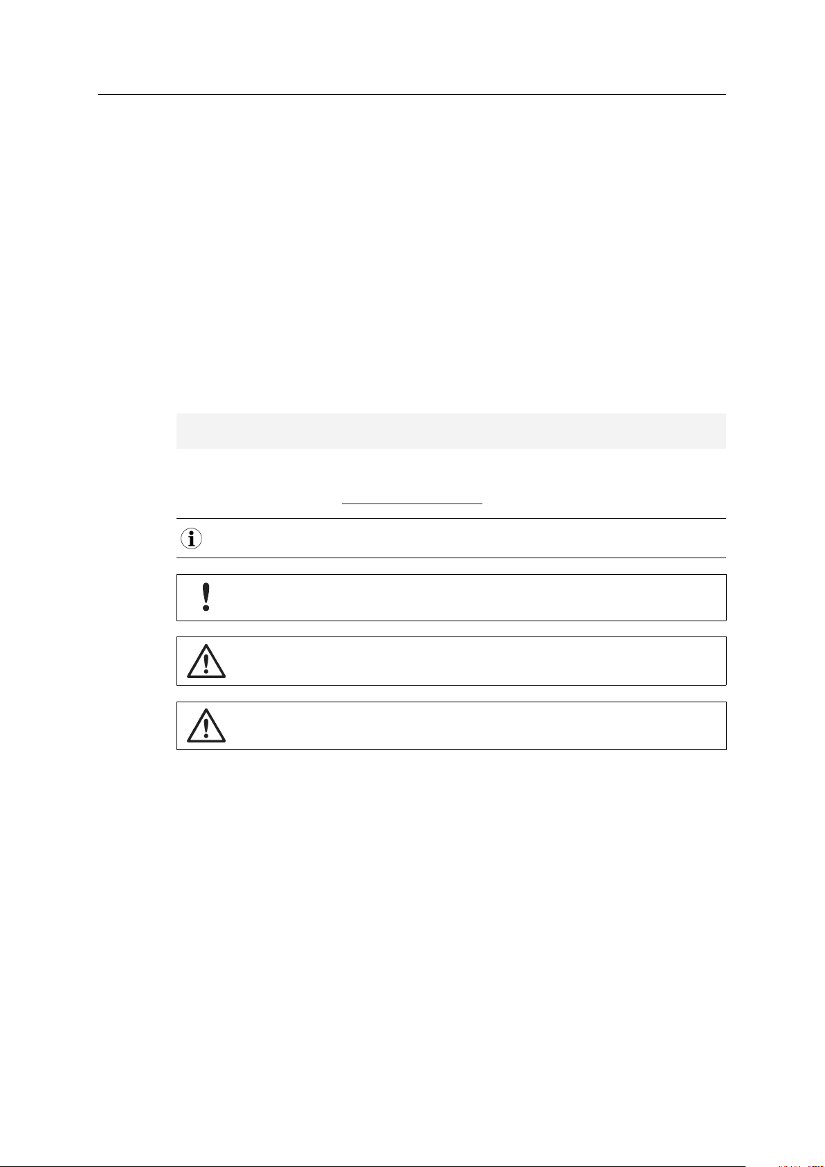
3 Host Interface
This chapter describes the low level properties of the Anybus CompactCom interface.
3.1 Overview
The Anybus CompactCom has five different host communication interfaces, corresponding to
different operating modes. The figure below illustrates the basic properties of these interfaces as
well as various I/O and control signals, and how they relate to the host application.
Fig. 1
Please note that only one communication interface at a time is available. Which one is decided
at startup.
3.1.1 Parallel Interface, 8-bit or 16-bit
From an external point of view, the parallel interface is a common 8-bit or 16-bit parallel slave
port interface, which can easily be incorporated into any microprocessor based system that has
3.1.2 SPI
Anybus®CompactCom B40-1 Design Guide
implementing an 8-bit or 16-bit wide SRAM. Additionally, the parallel interface features an
interrupt request line, allowing the host application to service the module only when actually
needed.
The Serial Peripheral Interface (SPI) is a synchronous serial link. It operates in full duplex mode
and devices communicate in master/slave mode where the Anybus CompactCom modules
always act as slaves. The interface can provide much higher performance than the serial
interface, but not as high as the parallel interface.
an external address/data bus. Generally, implementing this type of interface is comparable to
HMSI-27-230 3.4 en-US
Page 11

Host Interface 9 (78)
3.1.3 Stand-Alone Shift Register Interface
In this mode the Anybus CompactCom B40-1 operates stand-alone, with no host processor.
Process data is communicated to the shift registers on the host.
3.1.4 Serial Interface (UART)
The serial interface is provided for backward compatibility with the Anybus CompactCom 30. The
interface is event based, and has lower performance than the SPI and parallel modes. For more
information about the serial interface, see the Anybus CompactCom Hardware Design Guide for
the 30 series.
Please note that the Anybus CompactCom B40-1 is not backward compatible to the Anybus
CompactCom B30 hardware wise.
3.1.5 LED Interface
The status of the network LEDs is available as follows:
• As LED output signals on the network interface connector. These signals are able to drive a
LED directly and are available for all networks and operating modes. (Recommended)
• As LED output signals on the host interface connector for all operating modes except 16-bit
parallel mode. These signals are not able to drive a LED directly.
• In the LED status register for all modes, see Anybus CompactCom 40 Software Design guide
for more information.
3.1.6 Reduced Media-Independent Interface (RMII)
This interface is used for Transparent Ethernet, where Industrial Ethernet communication is
handled by the Anybus CompactCom and other Ethernet communication is routed to the host
application. 16–bit parallel mode and the LED Interface signals are not available in the host
application connector when Transparent Ethernet is enabled. The LED signals are still available
on the network connector of the Anybus CompactCom B40-1.
See RMII — Reduced Media-Independent Interface, p. 17 for mor information.
Anybus®CompactCom B40-1 Design Guide
HMSI-27-230 3.4 en-US
Page 12
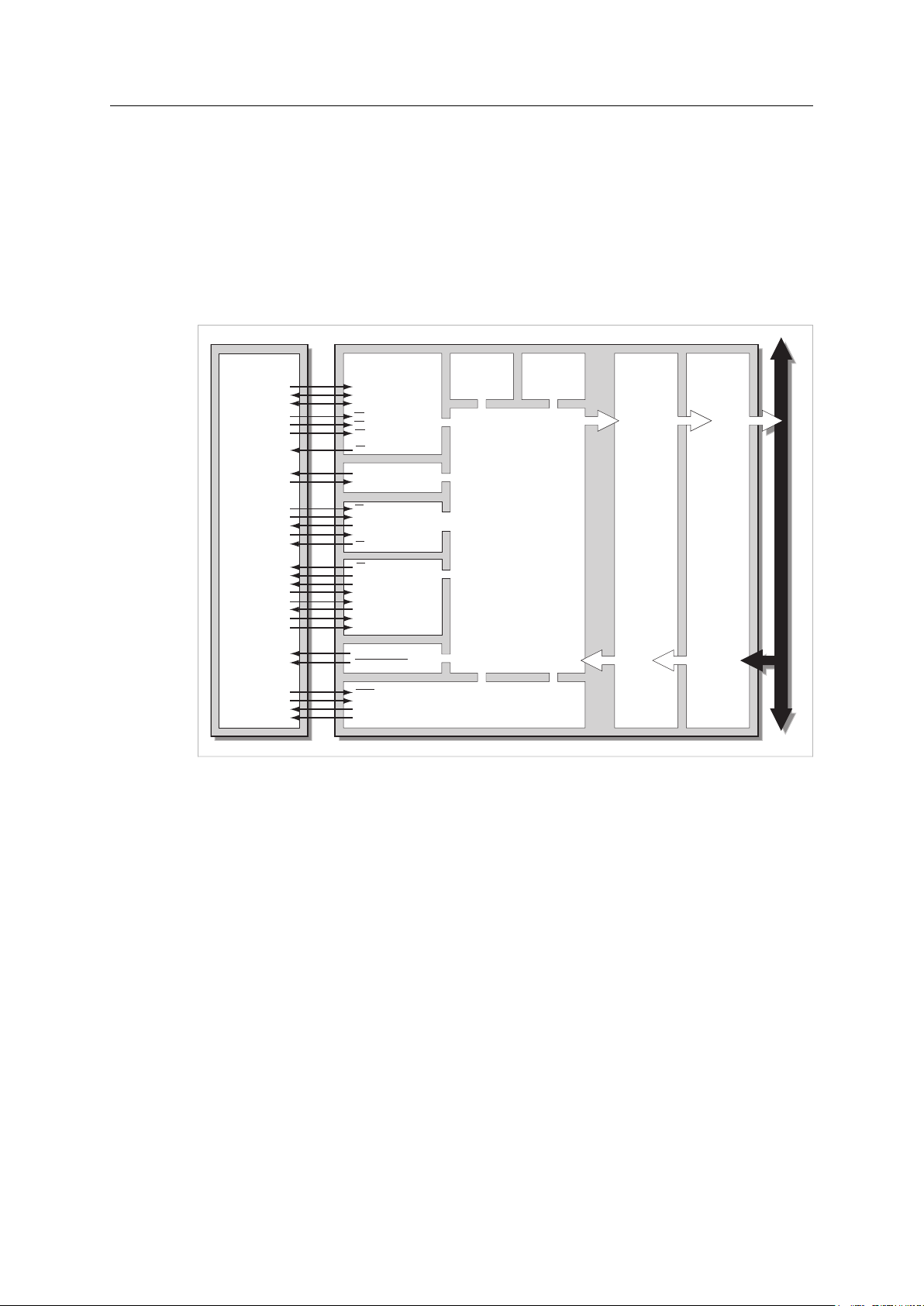
Host Interface 10 (78)
Pin 1
Application
interface
Pin 1
Network
interface
Outline of brick
Top view
1
2
56
55
Top view
3.2 Host Application Connector
The host application connector provides an interface between the host application and the
Anybus CompactCom B40-1.
Fig. 2
The connector is implemented by a standard 1.27 mm 56 pin header surface mounted to the
bottom side of the PCB.
Fig. 3
The pictures shows the pinning of the mating connector on the host application seen from the
top.
Anybus®CompactCom B40-1 Design Guide
HMSI-27-230 3.4 en-US
Page 13

Host Interface 11 (78)
GND 2 1 3V3
A0/WEH/DIP1_0 4
3 RESET
A2/DIP1_2 6
5 A1/DIP1_1
GND 8
7 A3/DIP1_3
A5/DIP1_5 10
9 A4/DIP1_4
A7/DIP1_7 12
11 A6/DIP1_6
GND 14
13 A8/LD/SS
A10/DO/MISO 16
15 A9/SCLK
GND 18
17 A11/DI/MOSI
A13/ASI_TX 20
19 A12/ASI_RX
D6/DIP2_6 22
21 D7/DIP2_7
GND 24
23 D5/DIP2_5
D3/DIP2_3 26
25 D4/DIP2_4
GND 28
27 D2/DIP2_2
MD0 30
29 D1/DIP2_1
OM0 32
31 D0/DIP2_0
GND 34
33 OM1
CS 36
35 OM2
IRQ/PA 38
37 WE/WEL/CT
GND 40
39 OE
LED4B/D14 42
41 LED4A/D15
GND 44
43 LED3A/D13
LED2A/D11 46
45 LED3B/D12
LED1A/D9 48
47 LED2B/D10
GND 50
49 LED1B/D8
TX/ASI_TX/OM3 52
51 RX/ASI_RX
MI0/SYNC 54
53 MI1
GND 56
55 3V3
Anybus®CompactCom B40-1 Design Guide
Fig. 4
See Pin Overview, p. 12 for information on how each pin is used in the different modes.
HMSI-27-230 3.4 en-US
Page 14

Host Interface 12 (78)
3.2.1 Pin Overview
Depending on operating mode, the pins have different names and different functionality.
Presented below is an overview of all pins except GND and 3V3.
The pin types of the connector are defined in PIN Types, p. 5. The pin type may be different
depending on which mode is used.
The ASI (Anybus Safety Interface) signals are used to connect a safety module to the safety interface of
an Anybus CompactCom 40-series module.
Note: The pin numbers of the Anybus CompactCom B40 (brick) host application
connector are different from those of the Anybus CompactCom M40 (module) host
application connector.
Pin Signal Name
Serial
Mode
4 DIP1_0 DIP1_0 A0 WEH DIP1_0 I
5 DIP1_1 DIP1_1 A1 A1 DIP1_1 I
6 DIP1_2 DIP1_2 A2 A2 DIP1_2 I
7 DIP1_3 DIP1_3 A3 A3 DIP1_3 I
9 DIP1_4 DIP1_4 A4 A4 DIP1_4 I
10 DIP1_5 DIP1_5 A5 A5 DIP1_5 I
11 DIP1_6 DIP1_6 A6 A6 DIP1_6 I
12 DIP1_7 DIP1_7 A7 A7 DIP1_7 I
13 SS A8 A8 LD
15 SCLK A9 A9 SCLK O, I
16 MISO A10 A10 DO O, I
17 MOSI A11 A11 DI I
19 ASI RX A12 A12 I
20 ASI TX A13 A13 O, I
31 DIP2_0 DIP2_0 D0 D0 DIP2_0
29 DIP2_1 DIP2_1 D1 D1 DIP2_1
27 DIP2_2 DIP2_2 D2 D2 DIP2_2
26 DIP2_3 DIP2_3 D3 D3 DIP2_3
25 DIP2_4 DIP2_4 D4 D4 DIP2_4
23 DIP2_5 DIP2_5 D5 D5 DIP2_5
22 DIP2_6 DIP2_6 D6 D6 DIP2_6
21 DIP2_7 DIP2_7 D7 D7 DIP2_7
49 LED1B LED1B LED1B D8 LED1B
48 LED1A LED1A LED1A D9 LED1A
47 LED2B LED2B LED2B D10 LED2B
46 LED2A LED2A LED2A D11 LED2A
45 LED3B LED3B LED3B D12 LED3B
43 LED3A LED3A LED3A D13 LED3A
42 LED4B LED4B LED4B D14 LED4B
41 LED4A LED4A LED4A D15 LED4A
37 WE WEL CT I
39 OE OE I
36 CS CS I
38 IRQ IRQ IRQ PA O
SPI Mode 8-bit
Mode
16-bit
Mode
Shift
Register
Mode
Type Notes
I/O
I, I/O
I, I/O
I, I/O
I, I/O
I, I/O
I, I/O
I, I/O
I, I/O
O, I/O
O, I/O
O, I/O
O, I/O
OD, I/O
OD, I/O
O, I/O
O, I/O
In modules supporting RMII,
these pins are used for the RMII
interface when this has been
activated, see RMII — Reduced
Media-Independent Interface, p.
17.
Anybus®CompactCom B40-1 Design Guide
HMSI-27-230 3.4 en-US
Page 15

Host Interface 13 (78)
Pin Signal Name
Serial
Mode
51 RX ASI RX ASI RX ASI RX ASI RX I
52
TX / OM3 ASI TX /
32 OM0 OM0 OM0 OM0 OM0 I
33 OM1 OM1 OM1 OM1 OM1 I
35 OM2 OM2 OM2 OM2 OM2 I
54 MI0
53 MI1 MI1 MI1 MI1 MI1 O
30 MD0 MD0 MD0 MD0 MD0 O
3 RESET RESET RESET RESET RESET I
SPI Mode 8-bit
OM3
MI0/SYNC MI0/SYNC MI0/SYNC MI0/SYNC
3.2.2 Power Supply Pins
Signal
GND Power 2, 8, 14, 18, 24,
3V3 Power 1, 55
Type
Mode
ASI TX /
OM3
16-bit
Mode
ASI TX /
OM3
Pin Description
28, 34, 40, 44,
50, 56
Ground
Power and signal ground reference.
3.3 V power supply.
Shift
Register
Mode
ASI TX /
OM3
Type Notes
I/O
O
Strapping input with internal
weak pull-up during powerup.
To configure OM3, use an
external pull-up/pull-down of
1.0 to 2.2 kΩ. The pin changes to
output after powerup
Low at power-up and before
reset release.
Tied to 3V
Tied to GND
Anybus®CompactCom B40-1 Design Guide
HMSI-27-230 3.4 en-US
Page 16

Host Interface 14 (78)
3.2.3 LED Interface / D8–D15 (Data Bus)
Signal Name
LED1A / D9 O / I/O
LED1B / D8 O / I/O
LED2A / D11 O / I/O
LED2B / D10 O / I/O
LED3A / D13 OD / I/O
LED3B / D12 OD / I/O
LED4A / D15 O / I/O
LED4B / D14 O / I/O
Pin Type Pin
48
49
46
47
43
45
41
42
Description, LED Interface
LED 1 Indication A
• Green
LED 1 Indication B
• Red
LED 2 Indication A
• Green
LED 2 Indication B
• Red
LED 3 Indication A
• Green
• Mainly used for link/
activity on network port 1
on the Ethernet modules.
Pin is open-drain to maintain
backward compatibility with
existing applications, where this
pin may be tied to GND.
LED 3 Indication B
• Yellow or red, depending
on network
• Mainly used for link/
activity on network port 1
on the Ethernet modules
(yellow).
Pin is open-drain to maintain
backward compatibility with
existing applications, where this
pin may be tied to GND.
LED 4 Indication A
• Green
• Mainly used for link/
activity on network port 2
on the Ethernet modules.
LED 4 Indication B
• Yellow or red, depending
on network
• Mainly used for link/
activity on network port 2
on the Ethernet modules
(yellow)
Description, Data Bus
D9 Data Bus
• "D9" in 16-bit parallel
mode.
D8 Data Bus
• "D8" in 16-bit parallel
mode.
D11 Data Bus
• "D11" in 16-bit parallel
mode.
D10 Data Bus
• "D10" in 16-bit parallel
mode.
D13 Data Bus
• "D13" in 16-bit parallel
mode.
D12 Data Bus
• "D12" in 16-bit parallel
mode.
D15 Data Bus
• "D15" in 16-bit parallel
mode.
D14 Data Bus
• "D14" in 16-bit parallel
mode.
The LED signals are also available on the network connector as active high push/pull signals. Those
signals are easier to use for LEDs.
Anybus®CompactCom B40-1 Design Guide
HMSI-27-230 3.4 en-US
Page 17

Host Interface 15 (78)
3.2.4 Settings / Sync
Signal Name
OM0
OM1
OM2
OM3 (ASI TX) (TX)
MI0 / SYNC
MI1
MD0 O 30
ASI RX
ASI TX
RX
TX
Type
I
I
I
I (Used as OM3
during power up)
O
O
I
O
I
O
Pin Description
32
33
35
52
54
53
51
52
UART
operation:
19
20
51
52
Operating Mode
Used to select interface and baud rate, see below.
Module Identification
MI0 and MI1 can be used by the host application to determine
what type of Anybus CompactCom that is connected.
SYNC
On networks that support synchronous communication, a
periodic synchronization pulse is provided on the SYNC output.
The SYNC pulse is also available as a maskable interrupt using the
IRQ signal.
Module Detection
This signal can be used by the host application to determine that
an Anybus CompactCom is inserted into the slot, see Module
Detection, p. 16.
The signal is connected directly to GND on the Anybus
CompactCom.
Black Channel Communication
These signals can be connected to a safety module, e.g. to IXXAT
Safe T100 to provide a safe channel for black channel
communication
If not used, pin 51 (for UART operation pin 19) should be pulled
to 3V3.
Serial Communications Signals
®
Anybus
CompactCom B40-1 Design Guide
HMSI-27-230 3.4 en-US
Page 18

Host Interface 16 (78)
Operating Modes
These inputs select the interface that should be used to exchange data (SPI, stand-alone shift
register, parallel or serial) and, if the serial interface option is used, the operating baud rate. The
state of these signals is sampled once during startup, i.e. any changes require a reset in order to
have effect.
OM3 OM2 OM1 OM0
LOW LOW LOW LOW
LOW LOW LOW HIGH SPI
LOW LOW HIGH LOW
LOW LOW HIGH HIGH
LOW HIGH LOW LOW
LOW HIGH LOW HIGH
LOW HIGH HIGH LOW
LOW HIGH HIGH HIGH
HIGH LOW LOW LOW
HIGH LOW LOW HIGH
HIGH LOW HIGH LOW
HIGH LOW HIGH HIGH
HIGH HIGH LOW LOW
HIGH HIGH LOW HIGH
HIGH HIGH HIGH LOW
HIGH HIGH HIGH HIGH
LOW = V
HIGH = V
IL
IH
These signals must be stable prior to releasing the RESET signal. Failure to observe this may result in
faulty behavior.
Operating Mode
Reserved
Stand-alone shift register
Reserved
Reserved
Reserved
Reserved
16-bit parallel
8-bit parallel
Serial 19.2 kbps
Serial 57.6 kbps
Serial 115.2 kbps
Serial 625 kbps
Reserved
Reserved
Service Mode
Module Detection
This signal is internally connected to GND, and can be used by the host application to detect
whether a module is present or not. When connecting an external pull-up resistor, a low signal
indicates that a module is present.
If not used, leave this signal unconnected.
Module Identification
These signals indicate which type of module that is connected. It is recommended to check the
state of these signals before accessing the module.
MI1 MI0
LOW LOW
LOW HIGH
HIGH LOW
HIGH HIGH
LOW = V
HIGH = V
OL
OH
On modules supporting “SYNC”, MI0 is used as a SYNC signal during operation. MI0 should only be
sampled by the application during the time period from power up to the end of SETUP state.
Module Type
Active Anybus CompactCom 30
Passive Anybus CompactCom
Active Anybus CompactCom 40
Customer specific
Anybus®CompactCom B40-1 Design Guide
HMSI-27-230 3.4 en-US
Page 19

Host Interface 17 (78)
3.2.5 RMII — Reduced Media-Independent Interface
In RMII enabled modules, the pins described in the table below are used for the RMII
communication. They are set to tristate during startup, making it impossilbe to indicate e.g.
exception during setup. When setup is complete, they are set to inputs/outputs according to the
selected mode. See Anybus CompactCom 40 Software Design Guide for more information on
mode selection.
The 16-bit parallel mode can not be used when RMII is enabled
LED status will not be available when RMII is enabled.
Pin Signal Name
49 RXD0 O
48 RXD1 O
47 RXDV O
46 I
45 TXD0 I
43 TXD1 I
42 TXEN I
41 CLK I
Type Notes
3.2.6 IRQ (Interrupt Request)
Signal Name Pin Type Pin Description
IRQ O 38 Interrupt Request
The use of this signal is optional but highly recommended. Even if the host application lacks
interrupt capabilities, it is recommended to connect this signal to an input port to simplify
software design.
This signal must be pulled to 3V3 on the host application side to prevent spurious interrupts
during startup.
-
-
-
Not used (connect to external pull-down)
-
-
-
-
Active low interrupt signal.
Anybus®CompactCom B40-1 Design Guide
HMSI-27-230 3.4 en-US
Page 20
Host Interface 18 (78)
Power
/RESET
0V
3.3V
Power
On
Power
Stable
t
B
t
A
V
IL
V
IH
t
t
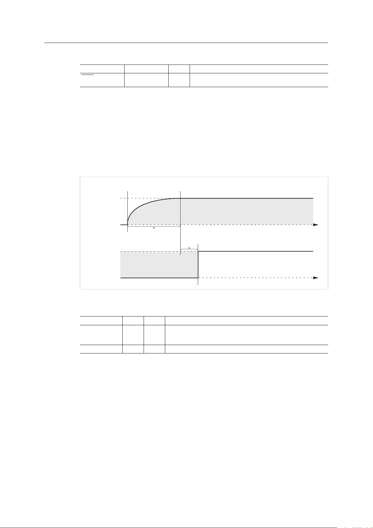
3.2.7 RESET (Reset Input)
Signal Name
Pin Type Pin Description
RESET I 3 Reset
Used to reset the module.
The master reset input is active low. It must be connected to a host application controllable
output pin in order to handle the power up sequence, voltage deviations and to be able to
support network reset requests. If the brick is used in stand-alone mode, with no host processor,
a separate reset circuit can be used, see Reset Circuit Example, p. 36.
The brick does not feature any internal reset regulation. To establish a reliable interface, the host
application is solely responsible for resetting the module when the supply voltage is outside the
specified range.
Power Up
Fig. 5
Powerup time limits are given in the table below:
Symbol Min.
t
A
t
B
- -
1 ms
Max.
-
Definition
Time until the power supply is stable after power-on; the duration depends
on the power supply design of the host application and is thus beyond the
scope of this document.
Safety margin.
Anybus®CompactCom B40-1 Design Guide
HMSI-27-230 3.4 en-US
Page 21

Host Interface 19 (78)
RESET
t
C
V
IL
V
IH
t
Restart
The reset pulse duration must be at least 10 µs in order for the NP40 to properly recognize a
reset.
Fig. 6
Symbol Min.
t
C
10 µs
Max.
-
Definition
Reset pulse width.
®
Anybus
CompactCom B40-1 Design Guide
HMSI-27-230 3.4 en-US
Page 22

Host Interface 20 (78)
3.3 Parallel Interface Operation
3.3.1 General Description
The parallel interface is based on an internal memory architecture, that allows the Anybus
CompactCom module to be interfaced directly as a memory mapped peripheral. The M40
modules can be configured for 8-bit or 16-bit parallel operation. The access time is 30 ns.
Polled operation is possible, but at the cost of an overhead. For increased efficiency, an optional
interrupt request signal (IRQ) can relieve the host application from polling for new information,
thus increasing the performance.
The parallel interface must be enabled using OM[0...3].
3.3.2 Pin Usage in 8-bit Parallel Mode
The parallel 8-bit interface uses the following signals:
Pin Signal Name Pin Type
4
5
6
7
9
10
11
12
13
15
16
17
19
20
31
29
27
26
25
23
22
21
49
48
47
46
45
43
42
41
37 WE I
39 OE I
36 CS I
38 IRQ O
32
33
35
A0
A1
A2
A3
A4
A5
A6
A7
A8
A9
A10
A11
A12
A13
D0
D1
D2
D3
D4
D5
D6
D7
LED1B
LED1A
LED2B
LED2A
LED3B
LED3A
LED4B
LED4A
OM0
OM1
OM2
I
I/O
O
O
O
O
OD
OD
O
O
I
Description/Comments
A[0...3]: Mandatory address input signals.
Standard bidirectional data bus.
8-bit mode: LED functionality, see LED Interface, p. 9.
Active low write signal or combined read/write signal.
Bus output enable; enables output on the data bus when low.
Bus chip select enable; enables parallel access to the module when
low.
Active low Interrupt Request signal. Asserted by the Anybus
CompactCom module.
The use of this signal is optional but highly recommended. Even if the
host application lacks interrupt capabilities, it is recommended to
connect this signal to an input port to simplify software design.
This signal must be pulled to 3V3 on the host application side to
prevent spurious interrupts during startup.
Operating mode. Connect all three to GND for 8-bit parallel operating
mode.
For more information see Operating Modes, p. 16.
Anybus®CompactCom B40-1 Design Guide
HMSI-27-230 3.4 en-US
Page 23

Host Interface 21 (78)
Pin Signal Name Pin Type
52
51 ASI RX I
54
53
30 MD0 O
3 RESET I
OM3 / ASI TX
MI0/SYNC
MI1
O, I
O
Description/Comments
Black channel output.
See Black Channel/Safety Interface, p. 51.
During startup the pin (with OM[0..2]) is used to define the operating
mode of the module. Connect to external pull-up for 8-bit parallel
operating mode, see Pin Overview, p. 12.
Black channel input. Tie to 3V3 if not used.
See Black Channel/Safety Interface, p. 51
See Module Identification, p. 16
See Module Detection, p. 16
See RESET (Reset Input), p. 18.
There are no internal pull-up resistors on any of the signals above, except for OM3, which has an internal
weak pull-up.
Function Table (CS, WE, OE, D[0...7])
CS WE OE
HIGH X X
LOW LOW X Data Input
LOW HIGH LOW Data Output
LOW HIGH HIGH
D[0...7] State
High
impedance
(Write)
(Read)
High
impedance
Comment
Module not selected.
Data on D[0...7] is written to location selected by
address bus.
Data from location selected by address bus is
available on D[0...7].
Module is selected, but D[0...7] is in a high
impedance state.
X = don’t care
LOW = V
HIGH = V
IL
IH
Anybus®CompactCom B40-1 Design Guide
HMSI-27-230 3.4 en-US
Page 24

Host Interface 22 (78)
3.3.3 Pin Usage in 16-bit Parallel Mode
The parallel 16-bit interface uses the following signals:
Pin Signal Name Pin Type
5
6
7
9
10
11
12
13
15
16
17
19
20
31
29
27
26
25
23
22
21
49
48
47
46
45
43
42
41
4 WEH I
37 WEL I
39 OE I
36 CS I
38 IRQ O
32
33
35
54
53
52
51 ASI RX I
30 MD0 O
3 RESET I
A1
A2
A3
A4
A5
A6
A7
A8
A9
A10
A11
A12
A13
D0
D1
D2
D3
D4
D5
D6
D7
D8
D9
D10
D11
D12
D13
D14
D15
OM0
OM1
OM2
MI0/SYNC
MI1
OM3 / ASI TX
I
I/O
I
O
O, Strap
Description/Comments
A[1...13]: Mandatory address input signals.
Selects source/target location.
Standard bidirectional data bus.
Write enable high byte.
Write enable low byte.
Bus output enable; enables output on the data bus when low.
Bus chip select enable; enables parallel access to the module when
low.
Active low Interrupt Request signal. Asserted by the Anybus
CompactCom module.
The use of this signal is optional but highly recommended. Even if the
host application lacks interrupt capabilities, it is recommended to
connect this signal to an input port to simplify software design.
This signal must be pulled to 3V3 on the host application side to
prevent spurious interrupts during startup.
Operating mode. Connect all three to 3V3 for 16-bit parallel operating
mode.
For more information see Operating Modes, p. 16
See Module Identification, p. 16
Black channel output.
See Black Channel/Safety Interface, p. 51
During startup the pin (with OM[0..2]) is used to define the operating
mode of the module. Connect to pull-down for 16-bit parallel
operating mode, see Pin Overview, p. 12.
Black channel input. Connect to 3V3 if not used.
See Black Channel/Safety Interface, p. 51
See Module Detection, p. 16.
See RESET (Reset Input), p. 18
The A0 signal is not needed in 16-bit parallel operating mode, as 16 bits are addressed instead of
8 bits. If there is need for writing one byte at the time signals WEH and WEL can be used to
enable writing to the high or low byte respectively. If both are enabled both bytes are written.
Anybus®CompactCom B40-1 Design Guide
HMSI-27-230 3.4 en-US
Page 25

Host Interface 23 (78)
Function Table (CS, WEL, WEH, OE, D[0...15])
CS WEL WEH OE
HIGH X X X
LOW LOW HIGH X
LOW HIGH LOW X
LOW LOW LOW X
LOW HIGH HIGH LOW
LOW HIGH HIGH HIGH
D[0...15] State
High impedance Module not selected.
Data Input (Write) Data on D[0...7] is written to low byte of
Data Input (Write) Data on D[8...15] is written to high byte
Data Input (Write) Data on D[0 ...15] is written to location
Data Output (Read) Data from location selected by address
High impedance Module is selected, but D[0...15] is in a
Comment
location selected by address bus.
of location selected by address bus.
selected by address bus.
bus is available on D[0...15].
high impedance state.
X = don’t care
LOW = V
HIGH = V
IL
IH
Anybus®CompactCom B40-1 Design Guide
HMSI-27-230 3.4 en-US
Page 26
Host Interface 24 (78)
Address
CS
OE
Data
Data valid
Data valid
tAA tAA
tACS
tAR
tHZ
tHZ
Address valid
Address valid
tDH
tRC
3.3.4 Memory Access Read Timing
The WE input signal must remain high during a read access. The timing diagram shows a burst
read, but the timing applies for a single read as well. The Anybus CompactCom B40-1 has no
setup or hold timing requirements on the address bus relative to CS during read operations. The
only limitation on read setup and hold times is that the pingpong and powerup interrupt will be
acknowledged if all address lines are high for 10-15 ns or more while CS is low.
Fig. 7
Symbol
tRC
tAA
tACS
tAR
tHZ
tDH
Parameter
Read cycle time
Address valid to Data valid
CS low to Data valid
OE low to Data valid
CS or OE high to output reached tristate
Data hold time
Min (ns) Max (ns)
30
-
-
-
-
0
-
30
30
15
15
-
Anybus®CompactCom B40-1 Design Guide
HMSI-27-230 3.4 en-US
Page 27
Host Interface 25 (78)
Address
CS
WE
Data
Data valid
Data valid
tAS tAH
tWP
Address valid
Address valid
tDHtDS
tWR
tAS tAH
tWP
tDHtDS
tWC
tWR
Address valid
Address
CS
WE
Data
Data valid
Data valid
tAS tAH
tWP
Address valid
Address valid
tDHtDS
tWR
tAS tAH
tWP
tDHtDS
tWC
tWR
Address valid
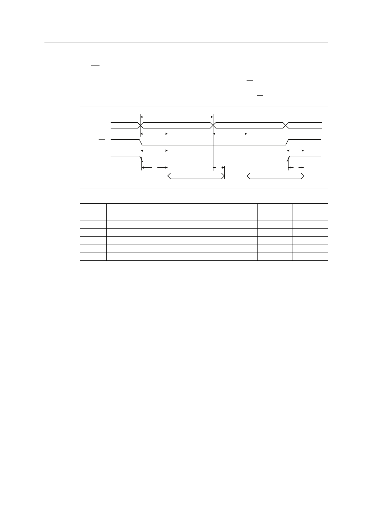
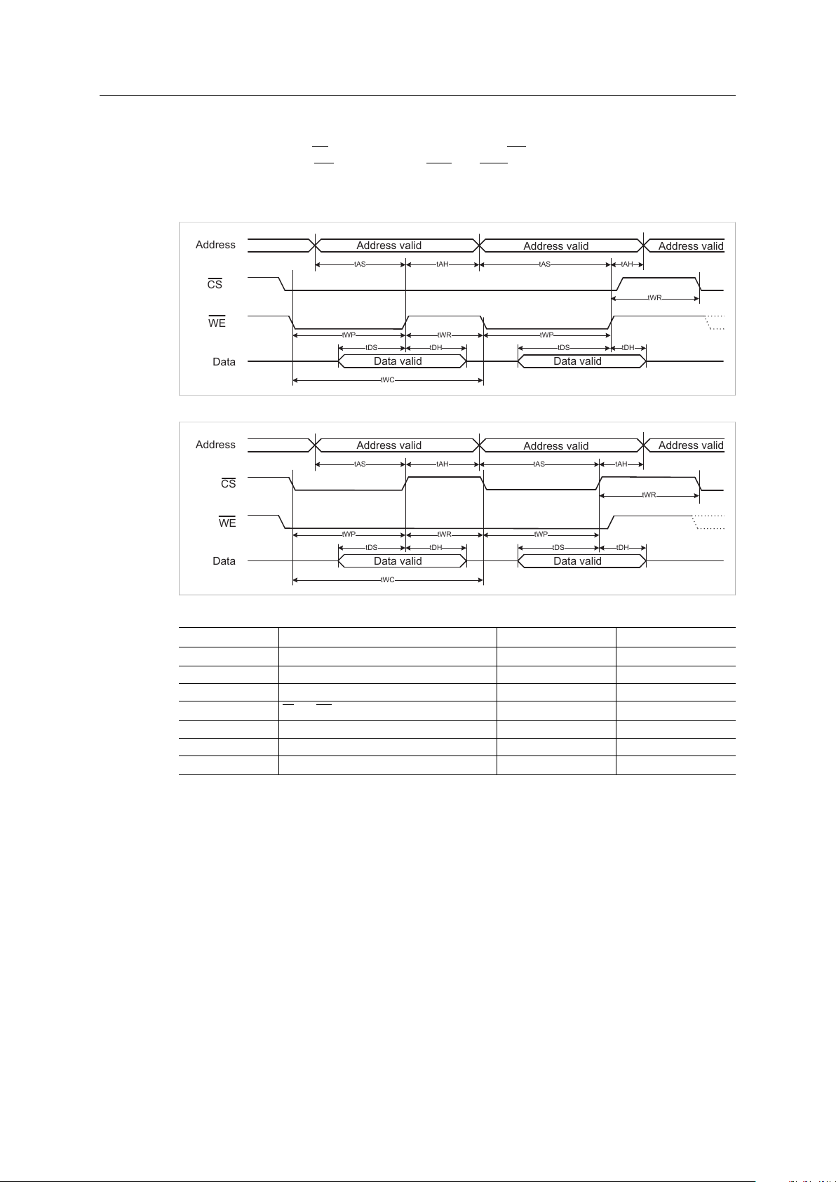
3.3.5 Memory Access Write Timing
It doesn’t matter if the OE signal is low or high as long as WE is active (low). In 16 bit mode, the
timing requirements of WE applies to both WEL and WEH. The timing diagrams show a burst
write but the timing applies for a single write as well. The first diagram shows write enable
controlled write timing and the second shows chip select controlled write timing.
Fig. 8
Fig. 9
Symbol
tWC
tAS
tAH
tWP
tDS
tDH
Parameter
Write cycle time
Address valid before End-of-Write
Address valid after End-of-Write
CS and WE low pulse width
Data valid before End-of-Write
Data valid after End-of-Write
tWR Write recovery time 10
Min (ns) Max (ns)
30
15
0
15
15
0
-
-
-
-
-
-
-
Anybus®CompactCom B40-1 Design Guide
HMSI-27-230 3.4 en-US
Page 28

Host Interface 26 (78)
3.4 SPI Operation
3.4.1 General Description
The SPI (Serial Peripheral Interface) bus is a synchronous serial data link standard which operates
in full duplex mode.
The SPI interface is activated using the OM[0...3] inputs. See Operating Modes, p. 16.
3.4.2 Pin Usage in SPI Mode
Presented below is an overview of all pins except GND and 3V3.
Pin Signal Name
4
5
6
7
9
10
11
12
13 SS I
15 SCLK I
16 MISO O
17 MOSI I
19
20
31
29
27
26
25
23
22
21
49
48
47
46
45
43
42
41
37
39
36
38 IRQ O
32
33
35
52
DIP1_0
DIP1_1
DIP1_2
DIP1_3
DIP1_4
DIP1_5
DIP1_6
DIP1_7
(not used)
DIP2_0
DIP2_1
DIP2_2
DIP2_3
DIP2_4
DIP2_5
DIP2_6
DIP2_7
LED1B
LED1A
LED2B
LED2A
LED3B
LED3A
LED4B
LED4A
(not used)
OM0
OM1
OM2
OM3 / ASI TX
Type
I
I
I
I
I
I
I
I
I
O, I
I
I
I
I
I
I
I
I
O
O
O
O
OD
OD
O
O
I Tie to 3V3.
I
O, Strap
Description/Comments
DIP switch. Usage defined by application.
Readable through attribute #14 (Switch status) in Anybus Object,
instance #1.
Tie to GND if not used.
Slave select. Active low.
Serial Clock Input
Master input, slave output. Input to the master’s shift register, and
output from the slave’s shift register.
Master output, slave input. Output from the master’s shift register,
and input to the slave’s shift register.
Tie to 3V3.
DIP switch. Usage defined by application.
Readable through attribute #14 (Switch status) in Anybus Object,
instance #1.
Tie to GND if not used.
LED interface. Gives access to LED indications. For more information,
see LED Interface / D8–D15 (Data Bus), p. 14".
Active low Interrupt Request signal. Asserted by the Anybus
CompactCom module.
The use of this signal is optional but highly recommended. Even if the
host application lacks interrupt capabilities, it is recommended to
connect this signal to an input port to improve the startup time.
This signal must be pulled to 3V3 on the host application side to
prevent spurious interrupts during startup.
Operating mode [OM2, OM1, OM0]: 0,0,1 for SPI operating mode.
For more information see Operating Modes, p. 16
Black channel output. See Black Channel/Safety Interface, p. 51
During startup the pin (with OM[0..2]) is used to define the operating
mode of the module. Connect to external pull-down for SPI operating
mode,see Pin Overview, p. 12.
Anybus®CompactCom B40-1 Design Guide
HMSI-27-230 3.4 en-US
Page 29

Host Interface 27 (78)
Pin Signal Name
51 ASI RX I
54
53
30 MD O
3 RESET I
MI0/SYNC
MI1
3.4.3 SPI Interface Signals
The SPI interface option uses three (optionally four) signals:
Signal
SCLK
MOSI
MISO
SS
For increased efficiency, the interrupt request signal (IRQ) is also available, allowing the host
application to service the Anybus CompactCom module only when necessary.
Description
Serial Clock Input
Master output, slave input. Output from the master’s shift register, and input to the slave’s shift
register.
Master input, slave output. Input to the master’s shift register, and output from the slave’s shift
register.
Slave Select (optional)
Type
O
Description/Comments
Black channel input. Connect to 3V3 if not used.
See Black Channel/Safety Interface, p. 51
See Module Identification, p. 16
See Module Detection, p. 16
See RESET (Reset Input), p. 18
Anybus®CompactCom B40-1 Design Guide
HMSI-27-230 3.4 en-US
Page 30

Host Interface 28 (78)
D0D1D2
D0D1D2
D0D1D2D3D4D5D7 D6
D0D1D2D3D4D5D7 D6
D0D1D2D3D4 D5D7 D6D5D7 D6
D0D1D2D3D4 D5D7 D6D5
SS
SCLK
MOSI
MISO
Byte 0 Byte NByte 1 Byte N-1
D7 D6
SCLK
MISO
MOSI
D7 D6 D5
D7 D6 D5
t
SU
t
HD
t
DO
t
CL
t
CH
SS
D0
D0
t
CSLZ
t
CSHZ
t
CSS
t
CSH
4–Wire Mode
In 4-wire mode the SS signal is used to indicate the start and stop of an SPI transfer. In this mode
the SCLK signal is allowed to be either idle high or idle low. This mode also allows multiple SPI
slaves on the same SPI bus, since Anybus CompactCom MISO is tri-stated when SS is high.
A 4-wire diagram example:
Fig. 10
Fig. 11
Item
tSU
tHD
tDO
tCL
tCH
tCL+tCH
Description
MOSI setup before SCK rising edge
MOSI hold after SCK rising edge
MISO change after SCK falling edge
SCK low period
SCK high period
SCLK period.
Min Value Max Value
10 ns
10 ns
-
-
0 ns 20 ns
20 ns
20 ns
50 ns
-
-
-
Max. frequency supported is 20 MHz.
tCSS
tCSH
tCSLZ
tCSHZ
SS setup before first SCLK rising edge.
SS hold after last SCLK rising edge.
MISO valid after falling edge of SS.
MISO high-Z after rising edge of SS.
20ns
20ns
-
-
-
-
20ns
20ns
Anybus®CompactCom B40-1 Design Guide
HMSI-27-230 3.4 en-US
Page 31

Host Interface 29 (78)
D0D1D2
D0D1D2
D0D1D2D3D4D5D7 D6
D0D1D2D3D4D5D7 D6
D0D1D2D3D4 D5D7 D6D5D7 D6
D0D1D2D3D4 D5D7 D6D5
SCLK
MOSI
MISO
Byte 0 Byte NByte 1 Byte N-1
D7 D6
MISO
SPI
CTRL
5 Words
Reserv
ed
MSGLEN
APP
STAT
INT
MASK
LEDSTAT
ANB
STAT
SPI
STAT
RdMsgField RdPdField
CRC
MOSI
MSG LEN Words
PD LEN Words
4 Words
2 Words
WrPdField CRC
1 WordMSG LEN Words
PD LEN Words 2 Words
PDLEN
Reserv
ed
Reserv
ed
NETTIME
WrMsgField PADDING
3–Wire Mode
In 3-wire mode the SS signal must be tied low permanently, and the SCLK signal must be idle high.
Multiple SPI slaves on the same bus are not possible in this mode. The module detects start and
stop of a transfer by monitoring SCLK activity.
There must be an idle period of at least 10 µs between two transfers in this mode, and the SCLK
signal must never remain high for more than 5 µs during a transfer.
A 3-wire diagram example.
Fig. 12
SPI diagram and bit timing for 3-wire mode.
Fig. 13
Item
tSU
tHD
tDO
tCL
tCH
tCL+tCH
Description Min Value Max Value
MOSI setup before SCK rising edge
MOSI hold after SCK rising edge
MISO change after SCK falling edge
SCK low period
SCK high period
SCK period
10 ns
10 ns
0 ns 20 ns
20 ns
20 ns
50 ns
-
-
-
-
-
Max. frequency supported is 20 MHz.
SPI Frame Format
Fig. 14
The bytes are transmitted with the most significant bit first. The byte order for non-byte frame
elements is typically little endian. This means that the least significant byte is transmitted first.
The CRC32 checksum is an exception as it is transmitted in big endian byte order (most
significant byte first).
Anybus®CompactCom B40-1 Design Guide
HMSI-27-230 3.4 en-US
Page 32

Host Interface 30 (78)
INPUT SHIFT
REGISTER 32
Input Byte 31Input Byte n-1
Output Byte 31Output Byte n-1
OUTPUT SHIFT
REGISTER 32
INPUT SHIFT
REGISTER 1
INPUT SHIFT
REGISTER 2
INPUT SHIFT
REGISTER 3
OUTPUT SHIFT
REGISTER 1
OUTPUT SHIFT
REGISTER 2
OUTPUT SHIFT
REGISTER 3
INPUT SHIFT
REGISTER n
Input Byte 0
Input Byte 1 Input Byte 2
Output Byte 0 Output Byte 1 Output Byte 2
OUTPUT SHIFT
REGISTER n
ADI #1 ADI #2
ADI #3
ADI #32
ADI #64 ADI #63
ADI #62
ADI #33
LD
SCLK
Input byte 0
DO
DI
Output byte 31 Output byte 30
Input byte 1
Output byte 0
Input byte 31
3.5 Stand-alone Shift Register
3.5.1 General Information
In this mode the Anybus CompactCom B40-1 operates stand-alone, with no host processor.
Process data is communicated to shift registers on the host. The Anybus CompactCom B40-1
supports up to 32 registers in each direction, for a total of 256 bits of data.
Fig. 15
Even though the Anybus CompactCom B40-1 operates stand-alone, it is still possible to set host
application attributes, via the use of the virtual attributes list. Some attributes are mandatory to
implement in order to pass conformance test. See the Virtual Attributes section in the Anybus
CompactCom 40 Software Design Guide for more information.
The Anybus CompactCom B40-1 will automatically detect the number of connected input and
output shift registers. Every shift register will be represented by one UINT8 ADI. The input ADIs
will be named “Input 0”, “Input 1”, etc. The output ADIs will be named “Output 0”, “Output 1”,
etc.
The ADI access descriptor values cannot be changed:
Input ADIs: 09h (Get access + Write process data mapping possible).
Output ADIs: 11h (Get access + Read process data mapping possible)
Bits are clocked out/in MSB first, on the positive side of CLK. An active low load signal (LD) loads
all shift registers before and after a transfer.
Fig. 16
A fifth signal, PA, is high when the module is in active state, and low when the module is not.
This signal can be used by the application to clear/set the output shift registers to default values
when the module is not in active state.
Anybus®CompactCom B40-1 Design Guide
HMSI-27-230 3.4 en-US
Page 33

Host Interface 31 (78)
3.5.2 Pin Usage in Stand-Alone Shift Register Mode
Presented below is an overview of all pins except GND and VDD.
Pin Signal Name
4
5
6
7
9
10
11
12
13 LD O
15 SCLK O
16 DO O
17 DI I
19
20
31
29
27
26
25
23
22
21
49
48
47
46
45
43
42
41
37 CT I
38 PA O
39
36
51 ASI RX I
52
32
33
35
54
53
30 MD O
3 RESET I
DIP1_0
DIP1_1
DIP1_2
DIP1_3
DIP1_4
DIP1_5
DIP1_6
DIP1_7
(not used)
(not used)
DIP2_0
DIP2_1
DIP2_2
DIP2_3
DIP2_4
DIP2_5
DIP2_6
DIP2_7
LED1B
LED1A
LED2B
LED2A
LED3B
LED3A
LED4B
LED4A
(not used)
(not used)
ASI TX / OM3
OM0
OM1
OM2
MI0/SYNC
MI1
Type
I
I
I
I
I
I
I
I
-
-
I
I
I
I
I
I
I
I
O
O
O
O
OD
OD
O
O
-
-
O, Strap
I
O
Description/Comments
DIP switch node address / IP address.
See DIP1 and DIP2 Pins Usage, p. 32.
Shift register load.
Clock output.
Serial data output to shift registers.
Serial data input from shift registers.
Leave unconnected
Leave unconnected
DIP switch baud rate / Device ID / station name.
See DIP1 and DIP2 Pins Usage, p. 32.
LED interface. Gives access to LED indications. For more information,
see LED Interface / D8–D15 (Data Bus), p. 14.
Center tap signal for shift register mode.
The number of connected input and output shift registers will be
detected using this signal.
Process active signal for shift register mode.
In a PROFINET shift register stand-alone application, the PA signal
must be used to clear outputs, when the Anybus CompactCom B40-1
is not in state PROCESS ACTIVE. Otherwise it will not be possible to
certify the final product. See the Anybus CompactCom 40 PROFINET
IRT Network Guide for more information.
Leave unconnected.
Leave unconnected.
Black channel input. Connect to 3V3 if not used.
See Black Channel/Safety Interface, p. 51
Black channel output.
See Black Channel/Safety Interface, p. 51
During startup the pin (with OM[0..2]) is used to define the operating
mode of the module. Connect to external pull-down for shift register
operating mode, see Pin Overview, p. 12.
Operating mode [OM2, OM1, OM0]: 0,1,0 for shift register operating
mode.
For more information seeOperating Modes, p. 16.
See Module Identification, p. 16.
See Module Detection, p. 16.
SeeRESET (Reset Input), p. 18
Anybus®CompactCom B40-1 Design Guide
HMSI-27-230 3.4 en-US
Page 34

Host Interface 32 (78)
DIP1 and DIP2 Pins Usage
The use of the DIP1 and DIP2 pins is network specific. If used, they will be read during SETUP
state. Thereafter, DIP switch changes will be sampled and written to the Network Configuration
Object every 0.5 seconds.
DIP1 is linked to the Network Configuration Object, instance 1 (node address) or instance 3 (IP
address). DIP2 is linked to the Network Configuration Object, instance 2 (baud rate) or instance 1
(Device ID, EtherCAT), or, in the case of PROFINET, linked to the PROFINET IO Object , instance 1,
attribute 24.
See Network Configuration Object (04h) in the Anybus CompactCom 40 Software Design Guide
for more information.
Network DIP1 (linked to Network
DeviceNet
EtherCAT 1 - 254 (Instance 3: IP
EtherNet/IP
Modbus-TCP 1 - 254 (Instance 3: IP
Common Ethernet 1 - 254 (Instance 3: IP
Ethernet
POWERLINK
PROFIBUS
Configuration Object)
0 - 63 (Instance 1: Node
address)
address)
1 - 254 (Instance 3: IP
address)
address)
address)
NMT_CS_BASIC_ETHERNET:
1 - 254 (Instance 3: IP
address)
NMT_CS_EPL_MODE:
1 - 239 (Instance 1: Node
address)
0 - 126 (Instance 1: Node
address)
DIP2 Notes
Value: 0 - 3 (Network
Configuration Object,
Instance 2: Baud Rate)
0 - 255 (Network
Configuration Object,
Instance 1: Device ID)
Not used
Not used
Not used
Not used If no POWERLINK traffic is seen at
Not used
DIP2: Network Configuration Object,
Instance 2: Baud Rate (125 kbps, 250
kbps, 500 kbps, Auto)
If DIP1 is set to 0, saved values from
instances 3 - 6 are used. If DIP1 is set
to 255, DHCP is used for all settings.
The DIP switches set the last byte of
the IP address. Virtual attributes are
used to configure the remaining part
the IP address, as well as the
subnetmask (Network Configuration
Object, instance 4) and the gateway
(instance 5).
startup the module will enter the
NMT_CS_BASIC_ETHERNET state
after 5 seconds. In this state DIP1 is
used for the IP address.
As soon as the module detects
POWERLINK traffic it will enter the
NMT_CS_EPL_MODE super state. In
this state DIP1 is used as the
POWERLINK node address. In the
NMT_CS_EPL_MODE state the IP
address of the module is fixed to
192.168.100.yyy where yyy is the
node address.
Note that IT functionality can be
disabled in the POWERLINK host
application object. If that is done
DIP1 is never used for the IP address.
-
®
Anybus
CompactCom B40-1 Design Guide
HMSI-27-230 3.4 en-US
Page 35

Host Interface 33 (78)
Network DIP1 (linked to Network
PROFINET
CC-Link 1 - 64 (Instance 1: Node
CC-Link IE Field 1 - 120 (Instance 1: Station
BACnet/IP
CANopen
Configuration Object)
1 - 254 (Instance 3: IP
address)
address).
Number).
1 - 254 (Instance 3: IP
address)
0 - 127 (Instance 1: Node
address)
DIP2 Notes
Value: 1 — 255 (PROFINET
IO object, Instance 1,
attribute 24)
Value: 0 - 4 (Network
Configuration Object,
Instance 2: Baud Rate)
1 - 239 (Instance 3: Network
Number).
Not used
Value: 0 - 9 (Network
Configuration Object,
Instance 2: Data Rate)
If DIP1 is set to 0, saved values from
instances 3 - 6 are used. If DIP1 is set
to 255, DHCP is used for all settings.
The DIP1 to switches set the last
byte of the IP address. Virtual
attributes are used to configure the
remaining part the IP address, as
well as the subnetmask (Network
Configuration Object, instance 4) and
the gateway (instance 5).
If DIP2 is set to 0, the value saved in
the non volatile memory will be used.
The DIP2 switches set the last three
digits of the station name. see the
Anybus CompactCom 40 PROFINET
IRT Network Guide.
DIP1: Depending on number of
stations used. An invalid value will
generate a NACK on Setup Complete.
DIP2: Network Configuration Object,
Instance 2: Baud Rate (156 kbps, 625
kbps, 2.5 Mbps, 5 Mbps, 10 Mbps)
-
-
DIP2: Network Configuration Object,
Instance 2: Data Rate
Unused DIP pins should be connected to ground (GND).
External pull-down resistors are needed if DIP switches are connected to the DIP1 and DIP2 pins,
see DIP Switches Example, p. 36.
Anybus®CompactCom B40-1 Design Guide
HMSI-27-230 3.4 en-US
Page 36

Host Interface 34 (78)
SCK
DI
DO
D7 D6 D5
D7 D6 D5
t
SUOtHDO
t
HDI
t
SUI
t
CH
LD
t
CL
D1 D0
D1 D0
CT
t
HDI
t
SUI
t
CH
t
CL
3.5.3 Timing
The Anybus CompactCom B40-1 operates in 12.5 MHz in shift register mode.
Timing Diagram
Fig. 17
Abbreviations from the diagram above, explained, and timing details:
Item
tSUO
tHDO
tSUI
tHDI
tCH
tCL
tCH + tCL
Description Min Value
DO setup before SCK rising edge
DO hold after SCK rising edge
DI/CT setup before SCK rising edge
DI/CT hold after SCK rising edge
SCK high period
SCK low period
SCK period
20 ns
20 ns
10 ns
0 ns
35 ns
35 ns
78 ns
The idle time between two transfers, i.e. when the LD signal is low, is at least 1 µs.
The cycle time range is typically 160 µs to 200 µs. However it is highly module and network
dependent, and may differ from the defined range.
Anybus®CompactCom B40-1 Design Guide
HMSI-27-230 3.4 en-US
Page 37

Host Interface 35 (78)
RCLR
RCLR
RCLR
RCLR
SRCLR
SRCLR
SRCLR
PL
Q7
Q7
Q7
Q7
Q7
CKE
CKE
I2 D4
O0 D5
I1 D0
I3 D0
I3 D2
I1 D6
O2 D7
O1 D7
O3 D2
I2 D7
I0 D1
O0 D7
O1 D1
O0 D3
O3 D5
O3 D6
O1 D5
OUTPUTS
I0 D6
I3 D7
O1 D3
I2 D2
O3 D3I3 D3
I1 D2
O3 D0
INPUTS
O0 D6
O2 D5
I2 D1
I0 D3
O3 D4
I2 D3
O1 D2
I0 D7
I1 D1
I3 D4
O0 D4
O0 D1
O2 D0
O1 D4
I2 D5
I0 D0
I3 D6
I0 D5
I0 D4
O2 D4
O2 D6
I1 D3
I2 D6
I1 D4
O2 D1
O2 D2
I1 D5
O0 D0
I3 D5
I3 D1
O2 D3
I1 D7
O1 D6
O0 D2
O3 D7
I2 D0
O3 D1
I0 D2
O1 D0
OUT_REG_3
74LVC594A
9
13
10
14
11
12 15
1
2
3
4
5
6
7
SDOSDI
SRCLK
RCLK A
B
C
D
E
F
G
H
OUT_REG_0
74LVC594A
9
13
10
+3.3V
14
11
12 15
1
2
3
4
5
6
7
SDO
SRCLR
SDI
SRCLK
RCLK A
B
C
D
E
F
G
H
OUT_REG_2
74LVC594A
9
13
10
14
11
12 15
1
2
3
4
5
6
7
SDOSDI
SRCLK
RCLK A
B
C
D
E
F
G
H
IN_REG_1
74LV165/SO
7
910
2
15
1
11
12
13
14
3
4
5
6
Q7
SDI
CLK
PL
A
B
C
D
E
F
G
H
IN_REG_0
74LV165/SO
7
910
2
15
1
11
12
13
14
3
4
5
6
Q7
SDI
CLK
CKE
PL
A
B
C
D
E
F
G
H
IN_REG_2
74LV165/SO
7
910
2
15
1
11
12
13
14
3
4
5
6
SDI
CLK
PL
A
B
C
D
E
F
G
H
OUT_REG_1
74LVC594A
9
13
10
14
11
12 15
1
2
3
4
5
6
7
SDOSDI
SRCLK
RCLK A
B
C
D
E
F
G
H
IN_REG_3
74LV165/SO
7
910
2
15
1
11
12
13
14
3
4
5
6
Q7
SDI
CLK
CKE
A
B
C
D
E
F
G
H
PA
Input byte 3
SR DO
Input byte 0
SR CLK
Output byte 2
Output byte 3
Output byte 0
SR LD_N
SR CT
Input byte 1
SR DI
(Pin 38, Optional)
(Pin 16)
(Pin 15)
(Pin 13)
(Pin 37)
(Pin 17)
Input byte 2
Output byte 1
+3.3V
+3.3V
+3.3V
3.5.4 Basic Shift Register Circuit
The schematic below illustrates a basic shift register circuit.
®
Anybus
CompactCom B40-1 Design Guide
Fig. 18
HMSI-27-230 3.4 en-US
Page 38

Host Interface 36 (78)
H_RESET_N
3V3
3V3
C2
1nF/50V
U?
TPS3828-33
RESET
1
GND
2
MR
3
WDI
4
VCC
5
R1
2k2
C1
100nF/16V
C3
1nF/50V
B1
SW PUSHBUTTON RIGHT ANGLE
1 2
3 4
DIP[1_0 .. 1_7]
DIP1_0
DIP1_1
DIP1_2
DIP1_3
DIP1_4
DIP1_5
DIP1_6
DIP1_7
DIP1_1
DIP1_2
DIP1_3
DIP1_4
DIP1_5
DIP1_6
DIP1_7
DIP1_0
3V3
10k10k10k 10k10k 10k10k10k
DIP switches
1
2
3
4
5
6
7
8
16
15
14
13
12
11
10
9
3.5.5 Reset Circuit Example
The reset circuit example in the figure, is a common 3.3 V supervisor. The main usage is to obtain
a defined reset release delay after the voltage is switched on. The power supply has to provide a
stable voltage within the interval 3.15–3.45 V
Fig. 19
3.5.6 DIP Switches Example
Pull-down resistors are necessary if DIP switches are connected to the DIP inputs.
Fig. 20
®
Anybus
CompactCom B40-1 Design Guide
HMSI-27-230 3.4 en-US
Page 39

Host Interface 37 (78)
3.6 UART Operation
3.6.1 General Description
The serial interface is a common asynchronous serial interface, which can easily be interfaced
directly to a microcontroller or UART. It is provided for backward compatibility with the Anybus
CompactCom 30 series.
The serial interface is activated using the OM[0...3] inputs, which also are used to select the
operating baud rate, see Operating Modes, p. 16.
Other communication settings are fixed to the following values:
Data bits: 8
Parity: None
Stop bits: 1
Communication settings are fixed to asynchronous, 8-N-1, with bit order LSB first and without
hardware flow control signals.
It is not possible to build a synchronous application in this mode.
Anybus®CompactCom B40-1 Design Guide
HMSI-27-230 3.4 en-US
Page 40

Host Interface 38 (78)
3.6.2 Pin Usage in Serial Mode
Presented below is an overview of all pins except GND and 3V3
Pin Signal Name Pin Type
4
5
6
7
9
10
11
12
13
15
16
17
19 ASI RX I
20 ASI TX O
31
29
27
26
25
23
22
21
49
48
47
46
45
43
42
41
37
39
36
38
51 RX I Receive Input
DIP1_0
DIP1_1
DIP1_2
DIP1_3
DIP1_4
DIP1_5
DIP1_6
DIP1_7
(not used)
(not used)
DIP2_0
DIP2_1
DIP2_2
DIP2_3
DIP2_4
DIP2_5
DIP2_6
DIP2_7
LED1B
LED1A
LED2B
LED2A
LED3B
LED3A
LED4B
LED4A
(not used)
(not used)
I
I
I
I
I
I
I
I
I
I
O,I
I
I
I
I
I
I
I
I
I
O
O
O
O
OD
OD
O
O
I
I
I
O
Description/Comments
DIP switch. Usage defined by application.
Readable through attribute #14 (Switch status) in Anybus Object,
instance #1.
Connect directly to GND if not used.
Connect directly to GND
Connect directly to 3V3.
See Black Channel/Safety Interface, p. 51
If not used, connect directly to 3V3.
See Black Channel/Safety Interface, p. 51
If not used, leave unconnected.
DIP switch. Usage defined by application.
Readable through attribute #14 (Switch status) in Anybus Object,
instance #1.
Connect directly to GND if not used.
LED interface. Gives access to LED indications. For more information,
LED Interface / D8–D15 (Data Bus), p. 14.
When not used, LED1A, LED1B, LED2A, LED2B, LED4A and LED4B can
be left unconnected.
LED3A and LED3B are open-drain outputs and should, if not used, be
pulled either to GND or to 3V3, depending on application.
Connect directly to 3V3.
Leave unconnected
• Direction: Host application -> CompactCom
• Idle state = High
Anybus®CompactCom B40-1 Design Guide
HMSI-27-230 3.4 en-US
Page 41

Host Interface 39 (78)
Pin Signal Name Pin Type
52
32
33
35
54
53
30 MD0 O
3 RESET I
TX / OM3
OM0
OM1
OM2
MI0/SYNC
MI1
It is important to connect all signals correctly for proper functioning of the serial interface.
3.6.3 Baud Rate Accuracy
Description/Comments
O, I Transmit Output
• Direction: CompactCom -> Host application
• Idle state = High
This pin doubles as OM3 strapping input on Anybus CompactCom
M40 modules. Connect a pull-up resistor on the application for this
pin in serial mode.
I
O
Operating mode [OM2, OM1, OM0]:
001
010
011
100
For more information see Operating Modes, p. 16.
See Module Identification, p. 16
See Module Detection, p. 16
See RESET (Reset Input), p. 18
Serial 19.2 kbps
Serial 57.6 kbps
Serial 115.2 kbps
Serial 625 kbps
As with most asynchronous communication devices, the actual baud rate used on the Anybus
CompactCom may differ slightly from the ideal baud rate.
The baud rate error of the module is less than ±1.5%. For proper operation, it is recommended
that the baud rate accuracy in the host application lies within ±1.5% from the ideal value.
Anybus®CompactCom B40-1 Design Guide
HMSI-27-230 3.4 en-US
Page 42

Network Connector 40 (78)
Pin 1
Application
interface
Pin 1
Network
interface
Outline of brick
Top view
1
2
52
51
Top view
4 Network Connector
The network connector provides network access to the brick.
Fig. 21
The signals from the brick network connector can be directly routed to the (optional) connector
board, which carries a network connector(s) identical or similar to the ones on the corresponding
Anybus CompactCom M40 module.
Examples on how to design the network access circuitry, when not using the connector board,
are shown in Design Examples, Network Interface, p. 74.
The brick has a standard 1.27 mm 52 pin header surface mounted to the bottom side of the
board as network interface.
Anybus®CompactCom B40-1 Design Guide
Fig. 22
The pictures shows the pinning of the corresponding network connector on the host application
board, seen from the top.
HMSI-27-230 3.4 en-US
Page 43

Network Connector 41 (78)
GND 2 1 3V3
B_1CEN/SDA 4
3 B_1P/RXP
GND 6
5 B_1N/RXN
B_2CEN/SCL 8
7 B_2P/SDP
GND 10
9 B_2N/SDN
B_3CEN 12
11 B_3P/TXEN
GND 14
13 B_3N/TXDIS
B_4CEN/BUSP 16
15 B_4P/TXP
GND 18
17 B_4N/TXN
NW_LED4A 20
19 NW_LED4B
NW_LED3A 22
21 NW_LED3B
NW_LED2A 24
23 NW_LED2B
NW_LED1A 26
25 NW_LED1B
GND 28
27 3V3
A_1CEN/SDA 30
29 A_1P/RXP
GND 32
31 A_1N/RXN
A_2CEN/SCL 34
33 A_2P/SDP
GND 36
35 A_2N/SDN
A_3CEN 38
37 A_3P/TXEN
GND 40
39 A_3N/TXDIS
A_4CEN/BUSP 42
41 A_4P/TXP
GND 44
43 A_4N/TXN
C_RX 46
45 C_TX
C_BUSP 48
47 C_TXEN
GATE2 50
49 GATE1
GND 52
51 3V3
Fig. 23
4.1 Overview
Depending on network, the pins have different names and different functionality. Presented
below is an overview of all pins except GND and 3V3. More detailed descriptions of the signals
are described for each network/fieldbus version later in this section (4).
Anybus®CompactCom B40-1 Design Guide
HMSI-27-230 3.4 en-US
Page 44

Network Connector 42 (78)
Pin Signal Name
Ethernet based
networks, Copper
3 B_1P B_RXP
4 B_1CEN B_SDA
5 B_1N B_RXN
7 B_2P B_SDP
8 B_2CEN B_SCL
9 B_2N B_SDN
11 B_3P B_TXEN
12 B_3CEN
13 B_3N B_XDIS
15 B_4P B_TXP
16 B_4CEN
17 B_4N B_TXN
19 NW_LED4B NW_LED4B NW_LED4B NW_LED4B NW_LED4B
20 NW_LED4A NW_LED4A NW_LED4A NW_LED4A NW_LED4A
21 NW_LED3B NW_LED3B NW_LED3B NW_LED3B NW_LED3B
22 NW_LED3A NW_LED3A NW_LED3A NW_LED3A NW_LED3A
23 NW_LED2B NW_LED2B NW_LED2B NW_LED2B NW_LED2B
24 NW_LED2A NW_LED2A NW_LED2A NW_LED2A NW_LED2A
25 NW_LED1B NW_LED1B NW_LED1B NW_LED1B NW_LED1B
26 NW_LED1A NW_LED1A NW_LED1A NW_LED1A NW_LED1A
29 A_1P A_RXP
30 A_1CEN A_SDA
31 A_1N A_RXN
33 A_2P A_SDP
34 A_2CEN A_SCL
35 A_2N A_SDN
37 A_3P A_TXEN
38 A_3CEN
39 A_3N A_TXDIS
41 A_4P A_TXP
42 A_4CEN
43 A_4N A_TXN
45 C_TX C_TX C_TX
46 C_RX C_RX C_RX
47 C_TXEN C_TXEN
48 C_BUSP_N
49 GATE1 GATE1 GATE1
50 GATE2 GATE2 GATE2
Ethernet based
networks, fiber optic
DeviceNet
PROFIBUS
CC-Link
At the moment the following copper wired Ethernet protocols are available: EtherNet/IP,
PROFINET IRT, Ethernet POWERLINK, EtherCAT, Modbus-TCP, CC-Link IE Field and BACnet/IP. At
the moment the following fiber optical Ethernet protocol is available: PROFINET IRT. The speed
of all of these protocols are 100 Mb/s (using signal pairs 1-2 of each port), except CC-Link IE Field
which is 1 Gb/s (using signal pairs 1–4 of each port).
The LED signals are active high and should be connected to respective LED via a resistor.
The pin types of the connector are defined in PIN Types, p. 5. The pin types are specified for each
network type on the following pages.
Anybus®CompactCom B40-1 Design Guide
HMSI-27-230 3.4 en-US
Page 45

Network Connector 43 (78)
4.2 Power Supply Pins
Signal Name
GND Power 2, 6, 10,
3V3 Power 1, 27, 51
Type
Pin No. Description
14, 18, 28,
32, 36, 40,
44, 52
Ground
Power and signal ground reference.
3.3 V power supply.
4.3 How to Connect Unused Network Connector Pins
For Ethernet versions of the Anybus CompactCom B40-1 it is recommended to terminate
Ethernet signals in the network interface if one of the Ethernet ports is unused. For the 10/100
Mb/s hardware version it is sufficient to terminate pair no. 1 and 2, for the port of concern,
while for the 1 Gb/s hardware version this has to be done for pair no. 1, 2, 3, and 4.
Fig. 24
Unused fibre optic connector pins should be connected as follows:
• 100R between TXP and TXN
• 820R between SDN and 3V3, resulting in 2 V on SDN
• 1k5 between SDP and 3V3, resulting in 1.5 V on SDP- Indicates that no signal is received. A
signal amplitude of 0.5 V is appropriate.
• 4k7 between SCL and 3V3
• 4k7 between SDA and 3V3
Other network signals may be left floating when not used.
Anybus®CompactCom B40-1 Design Guide
HMSI-27-230 3.4 en-US
Page 46

Network Connector 44 (78)
4.4 Ethernet Based Networks (Copper)
The industrial networks, that use Ethernet for communication, share the same hardware design.
However, the firmware downloaded to the brick is different depending on network. Physically
they use the same set of pins in a similar way. Bricks are available for the following Ethernet
based networks: EtherNet/IP, EtherCAT. PROFINET, Ethernet POWERLINK, CC-Link IE Field and
Modbus TCP.
The brick supports dual network ports, signal group A should be connected to the left port (port
1) and signal group B to the right port (port 2) on the connector board, looking at the front, see
Connector Board for Copper Based Ethernet, p. 55
For EtherCAT, signal group A is used for the IN port and signal group B is used for the OUT port.
Signal Group Signal Name Type
B B_1P
B_1CEN Power 4
B_1N
B_2P
B_2CEN Power 8
B_2N
B_3P
B_3CEN Power 12
B_3N
B_4P
B_4CEN Power 16
B_4N
A A_1P
A_1CEN Power 30
A_1N
A_2P
A_2CEN Power 34
A_2N
A_3P
A_3CEN Power 38
A_3N
A_4P
A_4CEN Power 42
A_4N
I/O
I/O
I/O
I/O
I/O
I/O
I/O
I/O
I/O
I/O
I/O
I/O
I/O
I/O
I/O
I/O
Pin
3
5
7
9
11
13
15
17
29
31
33
35
37
39
41
43
Description
First pair, positive signal
Center tap voltage for first pair
First pair, negative signal
Second pair, positive signal
Center tap voltage for second pair
Second pair, negative signal
Third pair, positive signal. Used for Gigabit Ethernet.
Center tap voltage for third pair. Used for Gigabit
Ethernet.
Third pair, negative signal. Used for Gigabit Ethernet.
Fourth pair, positive signal. Used for Gigabit Ethernet.
Center tap voltage for fourth pair. Used for Gigabit
Ethernet.
Forth pair, negative signal. Used for Gigabit Ethernet.
®
Anybus
CompactCom B40-1 Design Guide
HMSI-27-230 3.4 en-US
Page 47

Network Connector 45 (78)
4.5 Ethernet Fiber Optic Networks
Ethernet fiber optic networks use more or less the same pins as copper based Ethernet networks.
The brick supports PROFINET fiber optic network (PROFINET IRT).
The brick supports dual network ports, signal group A is be connected to the left port (port 1)
and signal group B to the right port (port 2)on the connector board, looking at the front, see
Connector Board for Fiber Optic Ethernet, p. 56.
If the Anybus CompactCom B40 connector board is not to be used, please study the design
requirements for the Rx and SD channels, see Rx Channel Design Requirements, p. 45 and SD
Channel Design Requirements, p. 46. Furthermore, fiber optic connectors without metal are
preferred in order to minimize EMC disturbance.
Signal Group Signal Name
B B_RXP I 3
B_SDA
B_RXN I 5
B_SDP I 7
B_SCL
B_SDN I 9
B_TXEN O 11
B_TXDIS O 13
B_TXP O 15
B_TXN O 17
A A_RXP I 29
A_SDA
A_RXN I 31
A_SDP I 33
A_SCL
A_SDN I 35
A_TXEN O 37
A_TXDIS O 39
A_TXP O 41
A_TXN O 43
Type
I/O
I/O
I/O
I/O
Pin Description
4
8
30
34
Rx, LVPECL positive signal
SDA, I2C data
Rx, LVPECL negative signal
Signal Detect, LVPECL positive signal
SCL, I2C clock
Signal Detect, LVPECL negative signal
Tx enable
TXEN is implemented as the inverse to TXDIS
Tx disable
Tx, LVPECL positive signal
Tx, LVPECL negative signal
Rx, LVPECL positive signal
SDA, I2C data
Rx, LVPECL negative signal
Signal Detect, LVPECL positive signal
SCL, I2C clock
Signal Detect, LVPECL negative signal
Tx enable
TXEN is implemented as the inverse to TXDIS
Tx disable
Tx, LVPECL positive signal
Tx, LVPECL negative signal
The differential signals Rx and Tx should be routed as differential pairs with a characteristic
impedance of 100 Ω differentially.
4.5.1 Rx Channel Design Requirements
The Rx channel is designed for an optical transceiver output that has an AC coupled 100 Ω
differential signal with 100-1000 mV amplitude, e.g. LVPECL (low voltage positive emitter
coupled logic). Each line is terminated with 50 Ω to a common point with a potential of 1.2 V on
the brick.
If a transceiver with a DC coupled output is used, series capacitors are needed to obtain desired
signal levels for the brick. Below is a figure describing three different options to connect a
transceiver output to an Rx channel on the brick:
Anybus®CompactCom B40-1 Design Guide
HMSI-27-230 3.4 en-US
Page 48

Network Connector 46 (78)
Brick
Trans-
ceiver
Trans-
ceiver
Trans-
ceiver
Brick Brick
AC coupled transceiver DC coupled transceiver DC coupled transceiver with bias current
Brick
Trans-
ceiver
Trans-
ceiver
Trans-
ceiver
Brick Brick
a: Differential
LVPECL output
b: Single ended LVPECL output
If the output is active low:
Connect the output to SDN and
the 820 Ω resistor to SDP .
c: LVCMOS output. If the output is
active low, connect the 1.8 kΩ
resistor to SDN instead.
Fig. 25
The AC coupling capacitors typically have a value of 100 nF. Resistors draining bias current
typically have a value of 150 Ω.
4.5.2 SD Channel Design Requirements
The SD (signal detect) channel is designed for a transceiver output that has a DC coupled
differential output with 100-1000 mV amplitude. If a transceiver with LVTTL/LVCMOS output is
used, the signal needs to be conditioned using a few resistors, to obtain desired signal levels for
the brick.
Each line is pulled to GND by a 1.27 kΩ resistor on the brick.
Even if the transceiver has a single ended output and the other line is at a fixed reference
potential, it is recommended to route SDN and SDP side by side all the way to the signal
conditioning resistors. This will give the interference, collected by the transmission line, common
mode characteristics, and it can thus be ignored by the differential input, instead of becoming a
differential mode interference that would corrupt the signal.
Below is a figure describing three different ways to connect a transceiver output to an SD
channel of the brick:
Fig. 26
In case a and case b, additional pull-down resistors will be required if the LVPECL outputs require
a certain bias current (> 1 mA) to function.
Anybus®CompactCom B40-1 Design Guide
HMSI-27-230 3.4 en-US
Page 49

Network Connector 47 (78)
4.6 DeviceNet
The Anybus CompactCom B40-1 DeviceNet communication interface uses the following pins:
Signal Name
C_TX O 45 Tx
C_RX I 46 Rx
C_BUSP_N I 48
GATE1 O 49
GATE2 O 50
For mechanical drawing of the applicable connector board see: Connector Board for CC-Link and
DeviceNet, p. 57
4.7 PROFIBUS
The Anybus CompactCom B40-1 PROFIBUS DP-V1 communication interface uses the following
pins:
Signal Name Type
C_TX O 45 Tx
C_RX I 46 Rx
C_TXEN O 47
GATE1 O 49
GATE2 O 50
Type
Pin Description
Bus power detection. Active low
Low voltage MOS gate driver. For fieldbus isolated DC supply circuitry.
The signals should preferably be routed to the connector board for
future compatitibility, but for DeviceNet, the isolated circuitry is
generally supplied by the bus power.
Pin
Description
TxEnable
Low voltage MOS gate driver. For fieldbus isolated DC supply circuitry.
Low voltage MOS gate driver. For fieldbus isolated DC supply circuitry.
For mechanical drawing of the applicable connector board see: Connector Board for PROFIBUS, p.
54 for information about the optional connector board.
4.8 CC-Link
The Anybus CompactCom B40-1 CC-Link communication interface uses the following pins:
Signal Name Type
C_TX O 45 Tx
C_RX I 46 Rx
C_TXEN O 47
GATE1 O 49
GATE2 O 50
For mechanical drawing of the applicable connector board see: Connector Board for CC-Link and
DeviceNet, p. 57 for information about the optional connector board.
Pin
Description
TxEnable
Low voltage MOS gate driver. For fieldbus isolated DC supply circuitry.
Low voltage MOS gate driver. For fieldbus isolated DC supply circuitry.
Anybus®CompactCom B40-1 Design Guide
HMSI-27-230 3.4 en-US
Page 50

Network Connector 48 (78)
Brick
network
interface
G
Y
220 Ω
220 Ω
NW_LED4A
NW_LED4B
4.9 LED Indicators
The Anybus CompactCom 40 series supports four bicolored LED indicators.
LED name Pin no.
LED1 26 NW_LED1A Green
25 NW_LED1B
LED2 24 NW_LED2A Green
23 NW_LED2B
LED3 22 NW_LED3A Green
21 NW_LED3B
LED4 20 NW_LED4A Green
19 NW_LED4B
Signal Name
Default color
Red
Red
Yellow
Yellow
Default Functionality
Network status
Module status
All Industrial
Ethernet Networks:
Other: Not used
EtherNet/IP,
Modbus-TCP
Other Not used
All Industrial
Ethernet Networks:
Other: Not used
EtherNet/IP,
Modbus-TCP
Other Not used
Link/Act for the
network port (port A)
10 Mbit Link/Act for
Link/Act for the
network port (port A)
Link/Act for the
network port (port B)
10 Mbit Link/Act for
Link/Act for the
network port (port B)
All LED outputs are active high and should be connected as shown in the picture below. The
resistor values should be chosen to get even light between different LEDs.
Fig. 27
4.9.1 Ethernet, 1000 Mbit
For Gigabit Ethernet applications, another solution for connecting the LEDs is needed to obtain
indications equal to the Anybus CompactCom M40. The solution, presented here, can be used
for 10 and 100 Mbit applications as well. The table below shows how to interpret the LED
indications in this case.
Please note that the only Anybus CompactCom 40 that at this time supports 1 Gbit communication over
Ethernet, is the Anybus CompactCom 40 CC-Link IE Field.
LEDxA LEDxB
Low Low
Low
High
High High Two green LEDs on for link detected, flickers to indicate 1 Gbit activity
All LED outputs are active high and should be connected as shown in the picture below.
Anybus®CompactCom B40-1 Design Guide
High Yellow LED on for link detected, flickers to indicate 10 Mbit activity
Low
Indication
Off
One green LED on for link detected, flickers to indicate 100 Mbit activity
HMSI-27-230 3.4 en-US
Page 51

Network Connector 49 (78)
Fig. 28
Anybus®CompactCom B40-1 Design Guide
HMSI-27-230 3.4 en-US
Page 52

EMC
5 EMC
This section offers information, necessary when designing in an Anybus CompactCom B40-1, to
ensure sufficient performance related to EMC. However, an engineering assessment is always
needed to ensure the quality. HMS Industrial Networks does not leave any guarantees, but
provides relevant information to the customers.
5.1 General
When working with a design in relation to EMC, it is recommended to always aim for good signal
integrity, since this is highly related to the EMC. For power, this means solid planes for both
power and GND together with good decoupling between the planes. As the quality of the power
is of great importance, it is important to perform sufficient verifications during the design
process to ensure this. This is also true for signals, where good signal integrity most likely results
in good EMC performance. There should always exist good connection to a reference plan
without any obstacles for the return current. Traces should also be kept short, with as few board
and cable transitions as possible, since every transition will have a negative impact on the signal
integrity.
For GND planes, the following basic design rules are important:
• A continuous and stable GND plane is needed underneath the B40 connectors in order to
ensure good signal integrity.
50 (78)
• The plane must follow the signal path through the connector
Considering the host application connector, different protocols are more sensitive to interference
than others. E.g. try to avoid using parallel and RMII interface in the design, if the
recommendations in this section cannot be followed or if the risk of interference is high. To
ensure stability, there has to be a sufficient separation on the host board between a parallel
interface and an RMII interface.
5.2 Bulk and Decoupling
Recommendations regarding bulk and decoupling capacitors is presented in Bypass Capacitance,
p. 73.
The capacitors have impact on the power quality at the Anybus CompactCom board, but are also
of importance in relation to EMC immunity. These general recommendations should be
evaluated for every design. The values may also need to be adjusted in relation to power
consumption, power quality on the main board, and the layout of the main board.
5.3 Reset Signal
There are several aspects to consider when routing the reset signal for the Anybus CompactCom.
Requirements for rise and fall time, but also the relation between the power up and the reset
signal are described in RESET (Reset Input), p. 18. These requirements must be met in all designs
to ensure stability. If the reset signal has a long trace or if there is any other aspect that has a
negative impact on the signal integrity, an RC filter may be required. To minimize the risk of EMC
problems, it is possible to add footprints for a RC-filter in advance and evaluate the need before
it becomes a problem during any certification. When designing the filter, all timing aspects must
be considered, so that the timing requirements in RESET (Reset Input), p. 18 are fulfilled.
Anybus®CompactCom B40-1 Design Guide
HMSI-27-230 3.4 en-US
Page 53

Black Channel/Safety Interface
M
PLC
Safety Controller
Safety
Module
Anybus
CompactCom
Motor Control
Black Channel
Safety Protocol Transportaon
Industrial Network
Anybus CompactCom
Network Interface
Safe T100
Scanner
6 Black Channel/Safety Interface
The black channel is a transportation mechanism for safety related protocol extensions over a
nonsafe communication media. The safety layer performs safety related transmission functions
and checks on the communication to ensure that the integrity of the link meets the requirement
for SIL 3, cat4/PL e. The black channel can be seen as a virtual link between the safety layers of
the devices.
51 (78)
Anybus®CompactCom B40-1 Design Guide
Fig. 29
The IXXAT Safe T100 is a precertified embedded safety option module which provides device
manufacturers with an easy and cost efficient way to integrate conformant safe I/O signals into
standard automation devices. It connects via its serial black channel interface to the Anybus
CompactCom module. The safety module provides digital safe I/O signals that can be controlled
via the network and that can be directly connected to the safety functions of an automation
device. Other standard safety modules can also be used to provide a safety communication
interface for the Anybus CompactCom 40 series.
The same serial interface is used both for serial download and for safety communication. Please
take this in account when implementing the use of a safety module or Black Channel.
HMSI-27-230 3.4 en-US
Page 54

This page intentionally left blank
Page 55

Appendix A: Mechanical Specification 53 (78)
36
36
33
13
2x
3,2
1,5 ± 0,25
2,3 ± 0,25
27 ± 0,20 4,5 ± 0,20
1,27 ± 0,05
1,27
2x26p
2x28p
8=max module height
Pin 1
Application
interface
Pin 1
Network
interface
Bottom view
A Mechanical Specification
This a class A product. In a domestic environment, this product may cause radio
interference in which case the user may be required to take adequate measures.
This product contains ESD (Electrostatic Discharge) sensitive parts that may be damaged if
ESD control procedures are not followed. Static control precautions are required when
handling the product. Failure to observe this may cause damage to the product.
All dimensions are in millimeters, tolerance ±0.10 mm, unless otherwise stated.
A.1 Anybus CompactCom B40-1
The dimensions for the Anybus CompactCom B40-1 are given in the picture below.
Fig. 30
Anybus
®
CompactCom B40-1 Design Guide
HMSI-27-230 3.4 en-US
Page 56

Appendix A: Mechanical Specification 54 (78)
1,5 ± 0,25
2,3 ± 0,25
3,5 ± 0,20
2,9
12,6
30,8
32
38,8
40
18
20
3,2
0,5
A.2 Connector Board for PROFIBUS
The connector board for the PROFIBUS network interface carries a D-sub connector
If the connector board is mounted in an environment that is subject to vibration, please
make sure to secure the network cable in such a manner, that the vibrations will not
harm the D-sub connector.
Anybus
Fig. 31
®
CompactCom B40-1 Design Guide
HMSI-27-230 3.4 en-US
Page 57

Appendix A: Mechanical Specification 55 (78)
1,5 ± 0,25
2,3 ± 0,25
3,5 ± 0,20
2,9 12,7
37,8
15,6
40
20
18
32
35
3,2
A.3 Connector Board for Copper Based Ethernet
The connector board for the copper based Ethernet network interfaces carries two RJ45
connectors.
Anybus
Fig. 32
®
CompactCom B40-1 Design Guide
HMSI-27-230 3.4 en-US
Page 58

Appendix A: Mechanical Specification 56 (78)
1,5 ± 0,25
2,3 ± 0,25
3,5 ± 0,20
2,9 13,2
40,3
16,8
20
40
18
32
44,5
3,2
A.4 Connector Board for Fiber Optic Ethernet
The connector board for the Fiber Optic Ethernet network interface carries two fibre optic
transceivers.
Fig. 33
®
Anybus
CompactCom B40-1 Design Guide
HMSI-27-230 3.4 en-US
Page 59

Appendix A: Mechanical Specification 57 (78)
1,5 ± 0,25
2,3 ± 0,25
3,5 ± 0,20
2,9 8,9
27,4
20
40
32
18
35
3,2
A.5 Connector Board for CC-Link and DeviceNet
The connector board for the CC-Link and the DeviceNet network interfaces carry a pluggable
screw terminal (5.08mm)
Fig. 34
®
Anybus
CompactCom B40-1 Design Guide
HMSI-27-230 3.4 en-US
Page 60

Appendix A: Mechanical Specification 58 (78)
33
2xM3
27
8,5
Pin 1
Application
interface
Pin 1
Network
interface
Outline of brick
Top view
A.6 Footprints
A.6.1 Anybus CompactCom B40-1
The Anybus CompactCom B40-1 is connected to the host application board through the host
application interface connector and a network interface connector. The footprint for the Anybus
CompactCom B40-1 is shown in the picture below.
Fig. 35
See Assembly, p. 60 for suggested components.
Anybus®CompactCom B40-1 Design Guide
HMSI-27-230 3.4 en-US
Page 61

Appendix A: Mechanical Specification 59 (78)
M3
14,5
Pin 1
Network
interface
FE
Outline of
connector board
Top view
1.5
2.3
27 4.5
8 = max module height
A.6.2 Network Connector Board
The network connectors are mounted on a separate connector board. The footprint for a
connector board is shown in the figure below. This footprint is the same for all connector boards
Fig. 36
The fastening screw must be connected to the functional earth (FE) of the host application.
See Assembly, p. 60 for suggested components.
A.7 Height Restrictions
All dimensions are in millimeters
Anybus®CompactCom B40-1 Design Guide
Fig. 37
The maximum height occupied by onboard components of the Anybus module is 8 mm. To ensure
isolation, it is recommended to add an additional 2.5 mm on top of these dimensions.
HMSI-27-230 3.4 en-US
Page 62

Appendix A: Mechanical Specification 60 (78)
20
40
32
18
0,5
3,2
2,0
Front plate placement area
A.8 Front Plate Restrictions
Customer applications that have a front plate with hole(s) for accessing the connector(s) of a
connector board, must have the front plate placed at least 0.5 mm away from the connector
board edge and must not reach further than 2.5 mm away from the connector board edge.
Fig. 38
A.9 Assembly
The Anybus CompactCom B40-1 and the connector board are mounted separately on to the host
application board. The connector board has to be secured using a screw, joining FE (functional
earth) on the connector board to FE on the host application board. The screw holes of the
Anybus CompactCom B40-1 are not connected to FE, but to GND. If suggested components are
used, the Anybus CompactCom B40-1 can be mounted without screws in a low vibration
environment, see Shock and Vibration, p. 63 for more information.
The Anybus CompactCom B40-1 can either be connected to the application board using headers,
or soldered directly to the host application PCB.
Anybus®CompactCom B40-1 Design Guide
HMSI-27-230 3.4 en-US
Page 63

Appendix A: Mechanical Specification 61 (78)
Fig. 39
Suggested components
Header Application interface Samtec CLP-128-02-L-D (56 pin)
Network interface Samtec CLP-126-02-L-D (52 pin)
Stand-off (M3)
Pemnet SMTSO-M3-4-ET
The screw standoffs are typically 4 mm tall. If the Anybus CompactCom B40-1 and connector
board are to be soldered directly to the host application board, standoffs should be 2 mm tall.
Outer diameter may be 6 mm max. The standoffs should not extend outside the screw mount
pads.
Recommended torque is 0.2 Nm. Locking paint kan be used to secure the screws against
loosening.
Anybus®CompactCom B40-1 Design Guide
HMSI-27-230 3.4 en-US
Page 64

Appendix A: Mechanical Specification 62 (78)
33
2xM3
M3
27
8,5 14,5
Pin 1
Application
interface
Pin 1
Network
interface
Pin 1
Network
interface
PCB layout
Standoffs, typ. 4 mm
FE
Outline of brick
Outline of
connector board
M3: Standoff with internal thread, size M3
Top view
Top view
Fig. 40
®
Anybus
CompactCom B40-1 Design Guide
HMSI-27-230 3.4 en-US
Page 65

Appendix B: Technical Specification 63 (78)
B Technical Specification
B.1 Environmental
B.1.1 Operating
-40 to 85° C (-40 to 185° F)
B.1.2 Storage
-40 to 85°C (-40 to 185° F)
B.1.3 Humidity
5 to 95% non-condensing
B.2 Shock and Vibration
B.2.1 Shock
The Anybus CompactCom B40-1 is tested according to IEC 68–2–27
• half-sine 30 g, 11 ms, 3 positive and 3 negative shocks in each of three mutually
perpendicular directions
• half-sine 50 g, 11 ms, 3 positive and 3 negative shocks in each of three mutually
perpendicular directions
Connector boards/interface cards are tested for 30 g.
B.2.2 Sinusoidal Vibration
The Anybus CompactCom B40-1 is tested according to IEC 68–2–6
Frequency range: 10–500 Hz
Amplitude 10–49 Hz:
Acceleration 50–500 Hz
Sweep rate:
0.35 mm
5 g
1 oct/min
10 double sweep in each of the three mutually perpendicular directions
B.3 Electrical Characteristics
Failure to follow the requirements may lead to permanent hardware damage
It is recommended for Anybus CompactCom B40-1 users to make sure that each signal
controlling the Anybus CompactCom B40-1 has a drive strength enough to fulfill level and timing
constraints even if the signal is loaded with 20 pF in parallel with 2.2 kΩ to GND or 3V3.
Anybus®CompactCom B40-1 Design Guide
HMSI-27-230 3.4 en-US
Page 66

Appendix B: Technical Specification 64 (78)
B.3.1 Operating Conditions
Symbol
3V3
GND Ground reference 0.00 0.00 0.00 V
I
IN
V
IH
V
IL
I
OH
I
OL
V
OH
V
OL
I
OH
(NW_
LEDx)
Parameter
Supply Voltage (DC)
Ripple (AC)
Current consumption
(also including network
interfaces and network
status LEDs)
Input High Voltage
Input Low Voltage
Current, Output High
Current, Output Low
Output High Voltage
Output Low Voltage
Output Current ,
network LEDs
Pin
Types
PWR
I, BI
O, BI
O 20 mA
Conditions Min.
3.15 3.30 3.45 V
- - ± 100 mV
-
Class A - - 250 mA
Class B - - 500 mA
Class C - - 1000 mA
-
-
= -4mA 2.4
I
OH
= 4mA
I
OL
2.0
-0.3
-8.0
- -
Typ.
-
-
-
- -
Max. Unit
3.45 V
0.8 V
8.0 mA
0.4 V
I= Input, CMOS (3.3V)
O= Output, CMOS (3.3V)
BI= Bidirectional, Tristate
PWR= Power supply inputs
V
B.4 Regulatory Compliance
EMC Compliance (CE)
Since the Anybus CompactCom is considered a component for embedded applications it cannot
be CE-marked as an end product.
However the Anybus CompactCom 40 family is pre-compliance tested in a typical installation
providing that all modules are conforming to the EMC directive in this installation.
The EMC pre-testing has been conducted according to the following standards:
Emission: EN61000-6-4 EN55016-2-3 Radiated emission
EN55022 Conducted emission
Immunity: EN61000-6-2 EN61000-4-2 Electrostatic discharge
EN61000-4-3 Radiated immunity
EN61000-4-4 Fast transients/burst
EN61000-4-5 Surge immunity
EN61000-4-6 Conducted immunity
Since all Anybus CompactCom B40-1 modules have been evaluated according to the EMC
directive through above standards, this serves as a base for our customers when certifying
Anybus CompactCom B40-1 based products.
Anybus®CompactCom B40-1 Design Guide
HMSI-27-230 3.4 en-US
Page 67

Appendix C: How to Disable Ethernet Port 2 (EtherNet/IP)
C How to Disable Ethernet Port 2 (EtherNet/IP)
It is possible to disable Ethernet Port 2 on the Anybus CompactCom B40-1 EtherNet/IP.
• Do not connect signal group B
• Do not connect signals LED4A/B
It is not possible to disable Ethernet Port 2 on any other Anybus CompactCom B40-1 than
EtherNet/IP.
For descriptions of signals see:
• Overview, p. 41
• Ethernet Based Networks (Copper), p. 44
• LED Indicators, p. 48
65 (78)
Anybus®CompactCom B40-1 Design Guide
HMSI-27-230 3.4 en-US
Page 68

Appendix D: Implementation Examples 66 (78)
D Implementation Examples
D.1 General
In this appendix HMS Industrial Networks provides examples of possible implementations for the
Anybus CompactCom B40-1 series.
There are many different processors with different functionality available on the market today.
The implementations in this appendix are to be regarded as examples that are designed for one
single type of processor. Other hardware interfaces may require adjustments for timing, different
functionality etc. It is important to fully understand the interface to take correct design decisions
in order to obtain a stable and reliable design.
Anybus®CompactCom B40-1 Design Guide
HMSI-27-230 3.4 en-US
Page 69

Appendix D: Implementation Examples 67 (78)
Host Application
CPU (3.3V)
3V3
3V3
SS
SCLK
MISO
MOSI
LED1B
LED1A
LED2B
LED2A
LED3B
LED3A
LED4B
LED4A
OM0
OM1
OM2
IRQ
RESET
MI0/SYNC
MI1
MD
SS
SCLK
MISO
MOSI
GPIO5
GPIO6
GPIO7
GPIO9
GPIO10
M40 pinning
OM3
3V3
D.2 SPI
This design is intended for an SPI implementation.
Fig. 41
If LEDs are to be used in the host application, please refer to Network Status LED Outputs (LED
[1A...4B]), p. 70, for guidelines on how to connect the LED outputs.
Anybus®CompactCom B40-1 Design Guide
HMSI-27-230 3.4 en-US
Page 70

Appendix D: Implementation Examples 68 (78)
Host Application
CPU (3.3V)
3V3
3V3
WEH
A8
A9
A10
A11
A12
A13
D8
D9
D10
D11
D12
D13
D14
D15
CS
OE
WEL
IRQ
RESET
MI0/SYNC
MI1
MD
A8
A9
A10
A11
A12
A13
D8
D9
D10
D11
D12
D13
D14
D15
CS
RD
WR/WR0
WR1
GPIO5
GPIO6
GPIO7
GPIO8
GPIO10
D0
D1
D2
D3
D4
D5
D6
D7
D0
D1
D2
D3
D4
D5
D6
D7
A1
A2
A3
A4
A5
A6
A7
A1
A2
A3
A4
A5
A6
A7
OM0
OM1
OM2
OM3
3V3
D.3 16-bit Parallel
This example shows a design for 16-bit parallel mode.
Fig. 42
If LEDs are to be used in the host application, please refer to Network Status LED Outputs (LED
[1A...4B]), p. 70, for guidelines on how to connect the LED outputs. In 16-bit parallel mode it is
not possible to use these outputs for LEDs. The network status LED signals are always present on
the network interface connector, see Network Connector, p. 40.
Anybus®CompactCom B40-1 Design Guide
HMSI-27-230 3.4 en-US
Page 71

Appendix D: Implementation Examples 69 (78)
Host Application
CPU (3.3V)
3V3 3V3
A8
A9
A10
A11
A12
A13
CS
RD
WR/WR0
GPIO5
GPIO6
GPIO7
GPIO9
GPIO10
A8
A9
A10
A11
A12
A13
LED1B
LED1A
LED2B
LED2A
LED3B
LED3A
LED4B
LED4A
CS
OE
WE
OM0
OM1
OM2
IRQ
RESET
MI0/SYNC
MI1
MD
A0
A1
A2
A3
A4
A5
A6
A7
A0
A1
A2
A3
A4
A5
A6
A7
D0
D1
D2
D3
D4
D5
D6
D7
D0
D1
D2
D3
D4
D5
D6
D7
M40 pinning
OM3
3V3
D.4 8-bit Parallel
This design is intended for 8-bit parallel mode.
Anybus®CompactCom B40-1 Design Guide
Fig. 43
If LEDs are to be used in the host application, please refer to Network Status LED Outputs (LED
[1A...4B]), p. 70, for guidelines on how to connect the LED outputs.
HMSI-27-230 3.4 en-US
Page 72

Appendix D: Implementation Examples 70 (78)
Host Application
CPU (3.3V)
3V3
3V3
3V3
OM0
OM1
OM2
Tx/OM3
Rx
IRQ
RESET
MI0/SYNC
MI1
MD
CS
RD
WR/WR0
WR1
Rx
Tx
GPIO5
GPIO6
GPIO7
GPIO8
GPIO10
GPIO1
GPIO2
GPIO3
LED1B
LED1A
LED2B
LED2A
LED3B
LED3A
LED4B
LED4A
3V3
D.5 Serial
The example in the figure below shows an implementation with serial communication.
Fig. 44
D.6 Network Status LED Outputs (LED[1A...4B])
All network status LED signals are easily available on the network interface connector. It is
recommended to use these signals when the network status is to be displayed. However they are
also available on the host interface connector (LED[1A...4B]).
The LED[1A....4B] outputs can be used to relay the network status LEDs to elsewhere on the host
application. This is possible in all modes except 16-bit parallel mode, where these pins are used
for data (D8...D15).
Note that it is the responsibility of the host application to ensure that each LED output is
connected to a LED of the correct color (it is possible to retrieve this information from the LED
status register or from the Anybus Object (01h); consult the Anybus CompactCom Software
Anybus®CompactCom B40-1 Design Guide
Design Guide for more information). For more information, see LED Interface / D8–D15 (Data
Bus), p. 14.
The outputs are unbuffered, and are not recommended for driving LEDs directly. Please consult
the image below for guidelines on how to connect the LED outputs.
HMSI-27-230 3.4 en-US
Page 73

Appendix D: Implementation Examples 71 (78)
3V33V3
3V3
3V3
3V3
LED1A
LED1B
LED2A
LED2B
LED3A
LED3B
LED4A
LED4B
CA
RTS
ACTIVE/PASSIVE*
*By connecting this signal to Ground, this design can be used to support Anybus CompactCom passive modules.
Fig. 45
These pins can not be used for LEDs in 16-bit parallel mode, as the pins in that case are used for data. All
network status LED signals are present on the network interface connector, and can be connected from
there.
Anybus®CompactCom B40-1 Design Guide
HMSI-27-230 3.4 en-US
Page 74

Appendix D: Implementation Examples 72 (78)
D.7 Power Supply Considerations
D.7.1 General
The Anybus CompactCom 40 platform in itself is designed to be extremely power efficient. The
exact power requirements for a particular networking system will however vary a lot depending
on the components used in the actual bus circuitry.
While some systems usually require less than 250 mA of supply current at 3.3 V, some high
performance networks, or networks which require the use of legacy ASIC technology, will
consume up to 500 mA, or in rare cases even as much as 1000 mA.
As an aid when designing the power supply electronics, the networks have been divided into
classes based on their power consumption as follows.
• Class A: less than 250 mA
• Class B: up to 500 mA
• Class C: up to 1000 mA
Please note that the power supply classifications take into account that the power budget is
shared with a full fieldbus circuitry, e.g. the appropriate connector board and NW_LEDs with
maximized consumption (20 mA each).
The following table lists the currently supported networking systems and their corresponding
class.
Network Class A Class B Class C
DeviceNet X
PROFIBUS X
CANopen X
EtherCAT
PROFINET 2-Port X
PROFINET FO 2-Port X
Ethernet/IP 2-Port
EtherNet POWERLINK
Common Ethernet
CC-Link
Modbus-TCP 2-Port
CC-Link IE Field
BACnet/IP
X
X
X
X
X
X
X
X
A power supply designed to fulfill Class A requirements (250 mA), will be able to support all
networks belonging to class A, but none of the networks in Class B and C.
A power supply designed to fulfill Class C requirements, will be able to support all networks.
Anybus®CompactCom B40-1 Design Guide
HMSI-27-230 3.4 en-US
Page 75

Appendix D: Implementation Examples 73 (78)
3V3
GND
C1
3.3 V
GND
5V
SS14
BAV70
22uF
(6.3V)
4k7
LT1767
10uH
100nF
(16V)
100nF
(16V)
1,5nF
(50V)
10uF
(6.3V)
Vin
FB
Vsw
GND
Vc
SHDN
SYNC
BOOST
VDD (3.3V)
GND
C1
C2
D.7.2 Bypass Capacitance
The power supply inputs must have adequate bypass capacitance for high-frequency noise
suppression. It is therefore recommended to add extra bulk capacitors near preferably all the
power supply inputs (or at least two):
Reference
C1
Fig. 46
D.7.3 3.3 V Regulation
The following example uses the LT1767 from Linear Technology to provide a stable 3.3 V power
source for the module. Note that all capacitors in this example are of ceramic type.
Value (Ceramic)
10 µF / 6.3 V
Fig. 47
For detailed information regarding this example, consult the data sheet for the LT1767 (Linear
Technology).
Anybus®CompactCom B40-1 Design Guide
HMSI-27-230 3.4 en-US
Page 76

Appendix E: Design Examples, Network Interface 74 (78)
Signal pair
Overall trace-to-trace length difference < 0.5 mm
Trace to trace length difference within each segment < 0.25 mm
Brick
Magnetics
RJ45
Connector
E Design Examples, Network Interface
If the optional connector board is used, the signals from the network interface connector of the
brick can be routed directly to the corresponding pins of the connector on the connector board.
Section E.2 shows an example PCB layout for this case.
This appendix also contains typical examples, of how to design the network interface, if the
optional connector board is not to be used. See Network Interface Examples, p. 77.
E.1 Recommendations
• The longer the distance between the Brick and the Connector board, the more important it
is that single-ended signals as well as signal pairs are separated from other signals and signal
pairs to maintain good signal integrity.
• All conductors should have a tighter coupling to a continuous ground plane than to any
adjacent conductor (even to the partner signal of a signal pair). All signal pairs should have a
differential impedance of 100 Ω ±10%.
It is not recommended to separate network circuitry, e.g. Connector board, and Brick more
than 400 mm. The distance should be kept shorter if the signals are adjacent to other
interfering circuitry. Radiated interference from the signals between the Connector board
and Brick may need to be taken care of by e.g. a metallic housing or encapsulating PCB
copper planes if the routing distance is long.
• If a design will be used for Gigabit Ethernet applications, the following has to be fulfilled:
– The maximum difference in length, between signal pairs (1 - 4) in the design must not
exceed 6.7 mm.
– The maximum difference in length, between the two signals in a signal pair must not
exceed 0.25 mm from Phy to Gigabit Magnetics and 0.25 mm from Gigabit Magnetics
to the Ethernet connector.
Fig. 48
• To avoid B40-1 connector pins penetrating the solder mask under the headers on the carrier
board, thus creating short circuits, the following is recommended:
– either use headers that are higher than 2.5 mm,
– or do not design any vias or traces on top side of the PCB, where there is any risk for
short circuits, see figure in section E.2.
• Minimum recommended power rating for termination/grounding resistors is 1/16 W.
Anybus®CompactCom B40-1 Design Guide
HMSI-27-230 3.4 en-US
Page 77

Appendix E: Design Examples, Network Interface 75 (78)
• DC/DC transformer selection recommendations:
– 1:2.1 turns ratio
– 500 kHz switching frequency
– The transformer shall be able to deliver at least 100 mA on the network interface side
without saturating, at Anybus CompactCom min/max supply voltage, and at the
relevant min/max ambient temperature that is applicable
– Under the above circumstances, the transformer and rectifier output voltage must
allow the regulator tokeep the 5V rail inside a ±5% tolerance
Anybus®CompactCom B40-1 Design Guide
HMSI-27-230 3.4 en-US
Page 78

Appendix E: Design Examples, Network Interface 76 (78)
E.2 PCB Layout
The pin headers of the Anybus CompactCom B40-1 have pins which are 2.3 mm tall nominally,
but to avoid risk of short circuit when the pin length is in the upper tolerance region, it is
suggested to have via/route keepouts on the PCB top layer, in between the pad rows, as the
figure shows, unless a receptacle taller than 2.6 mm is used.
Fig. 49
®
Anybus
CompactCom B40-1 Design Guide
HMSI-27-230 3.4 en-US
Page 79

Appendix E: Design Examples, Network Interface 77 (78)
E.3 Network Interface Examples
This section contains typical examples, of how to design the network interface, if the optional
connector board is not to be used. Examples are given for the usual network connectors as well
as for M12 connectors making a higher IP rating possible.
Example Schematics Brick
10 and 100 Mbit Ethernet
Network Interface(Copper)
100 Mbit Ethernet Network
Interface (Fiber Optic)
10 and 100 Mbit Ethernet
Network Interface (M12)
10, 100 and 1000 Mbit Ethernet
Network Interface
PROFIBUS PROFIBUS
PROFIBUS (M12)
DeviceNet DeviceNet
DeviceNet (M12)
CC-Link CC-Link
CANopen CANopen
EtherNet/IP
EtherCAT
Modbus TCP
Common Ethernet
POWERLINK
PROFINET IRT
BACnet/IP
PROFINET IRT
EtherNet/IP
EtherCAT
Modbus TCP
Common Ethernet
POWERLINK
PROFINET IRT
BACnet/IP
CC-Link IE Field RJ45 connector example: SS-60300-032 (Bel stewart)
PROFIBUS
DeviceNet
Comments
All bricks for 100 Mb/s Ethernet based protocols, running
on copper wire, use the same hardware.
Ethernet trafo example: 7490100111A (Würth Elektronik
Gmbh)
RJ45 connector example: SS-60300-032 (Bel stewart)
-
All bricks for 100 Mb/s Ethernet based protocols, running
on copper wire, use the same hardware.
Ethernet trafo example: 7490100111A (Würth Elektronik
Gmbh)
-
-
-
-
-
-
®
Anybus
CompactCom B40-1 Design Guide
HMSI-27-230 3.4 en-US
Page 80

5
4
3
2
1
Design Example
10 and 100 Mbit Ethernet
Network Interface
with RJ-45 connectors
D D
TR2
J6
1
2
3
4
5
6
7
8
9
10
11
12
13
14
15
16
17
18
C C
19
20
21
22
23
24
25
26
3V3
B_1P/RXP
B_1CEN/SDA
B_1N/RXN
B_2P/SDP
B_2N/SDN
B_3P/TXEN
B_3CEN/RX
B_3N/TXDIS
B_4P/TXP/TX
B_4CEN/CD/BUSP_N
B_4N/TXN/TX_N
NW_LED4B_N
NW_LED4A_N
NW_LED3B_N
NW_LED3A_N
NW_LED2B_N
NW_LED2A_N
NW_LED1B_N
NW_LED1A_N
B_1P
B_1N
B_1CEN
B_2CENB_2CEN/SCL
B_2P
B_2N
1 2
C2
100nF/16V
Ethernet Trafo
7490100111A (Würth Elektronik Gmbh)
C3
100nF/16V
TDB+ TDB+
TDB-
TDBRDB+
RDB-
RDB+
SHIELDB
RDB-
R2
75R
R3
75R
C4
1nF/2kV
R4
75R
R5
75R
C1
1nF/2kV
FE
J5
1
1
2
2
3
3
4
4
5
5
6
6
7
7
8
8
9
9
10
10
RJ-45 connector
SS-60300-032 (Bel stewart)
FE
R1
1M
27
28
29
30
31
32
33
34
35
36
37
38
39
40
B B
41
42
43
44
45
46
47
48
49
50
51
52
B40-1 connector
3V3
A_1CEN/SDA
A_1N/RXN
A_2P/SDP
A_2CEN/SCL
A_2N/SDN
A_3P/TXEN
A_3CEN/RX
A_3N/TXDIS
A_4P/TXP/TX
A_4CEN/CD/BUSP_N
A_4N/TXN/TX_N
C_TX
C_RX
C_TXEN
C_BUSP_N
GATE1
GATE2
3V3
A_1PA_1P/RXP
A_1N
A_1CEN
A_2CEN
A_2P
A_2N
3 4
C6
100nF/16V
Notes:
1,2,3,4) Place center tap capacitors close to the respective
transformer.
TR1
Ethernet Trafo
7490100111A (Würth Elektronik Gmbh)
C7
100nF/16V
TDA+ TDA+
TDA-
TDARDA+
RDA-
SHIELDA
RDA+
RDA-
R8
75R
R9
75R
C8
1nF/2kV
R6
75R
R10
75R
C5
1nF/2kV
FE
J4
1
1
2
2
3
3
4
4
5
5
6
6
7
7
8
8
9
9
10
10
RJ-45 connector
SS-60300-032 (Bel stewart)
FE
R7
1M
A A
5
4
3
2
1
Page 81

5
4
3
2
1
Design Example
3V3
J1, pin #1
C1
10uF/10V
D D
C C
B B
J1
1
2
3
4
5
6
7
8
9
10
11
12
13
14
15
16
17
18
19
20
21
22
23
24
25
26
27
28
29
30
31
32
33
34
35
36
37
38
39
40
41
42
43
44
45
46
47
48
49
50
51
52
3V3
B_1P/RXP
B_1CEN/SDA
B_1N/RXN
B_2P/SDP
B_2CEN/SCL
B_2N/SDN
B_3P/TXEN
B_3CEN/RX
B_3N/TXDIS
B_4P/TXP/TX
B_4CEN/CD/BUSP_N
B_4N/TXN/TX_N B_TXN
NW_LED4B_N
NW_LED4A_N
NW_LED3B_N
NW_LED3A_N
NW_LED2B_N
NW_LED2A_N
NW_LED1B_N
NW_LED1A_N
3V3
A_1P/RXP
A_1CEN/SDA
A_1N/RXN
A_2P/SDP
A_2CEN/SCL
A_2N/SDN
A_3P/TXEN
A_3CEN/RX
A_3N/TXDIS
A_4P/TXP/TX
A_4CEN/CD/BUSP_N
A_4N/TXN/TX_N
C_TX
C_RX
C_TXEN
C_BUSP_N
GATE1
GATE2
3V3
C2
100nF/16V
B_SDN
B_SDP
B_RXN
B_RXP
B_TXP
1
B_SDA
B_SCL
B_TXDIS
A_SDA
A_SCL
A_TXDIS
A_SDN
A_SDP
A_RXN
A_RXP
A_TXP
A_TXN
1
3V3
R5
820R
3V3
R3
150R
R8
150R
R6
820R
R2
0R
2
R1
0R
2
R4
150R
R9
150R
3V3
B_SDPA
B_RXNA
B_RXPA
A_SDPA
A_RXNA
A_RXPA
2
R10
4k7
R11
4k7
C15
100nF/16V
R12
4k7
C17
100nF/16V
C16
100nF/16V
R13
4k7
C18
100nF/16V
Ethernet Fibre Optics
Network Interface
5
4
3
2
1
SD
RD-
RxVCC
RxGND
12
5
4
3
2
1
SD
RD-
RxVCC
RxGND
12
3V3
3V3
3V3
3V3
6
RD+
TxVCC7TxGND8TxDIS9TD+10TD-11SCL
6
RD+
TxVCC7TxGND8TxDIS9TD+10TD-11SCL
Port B
U1
SDA
QFBR-5978Z
Port A
U2
SDA
QFBR-5978Z
14
GND#14
GND#13
13
14
GND#14
GND#13
13
Left port, seen from the front side Right port, seen from the front side
3V3
J1, pin #51
C5
10uF/10V
C6
100nF/16V
C3
100nF/16V
3V3 3V3 3V3 3V3
C4
4u7F/6V3
U1, pin #7U1, pin #3
C9
100nF/16V
C10
4u7F/6V3
C7
100nF/16V
C8
4u7F/6V3
U2, pin #7U2, pin #3
C11
100nF/16V
C12
4u7F/6V3
Notes:
1) RX and TX signal pairs shall have a differntial impedance of 100 Ohm.
2) Do not mount R1, R2, R5 and R6 if SD interface is not used.
A A
5
4
3
2
1
Page 82

5
4
3
2
1
Design Example
10 and 100 Mbit Ethernet
Network Interface
with M12 connectors
D D
TR2
J6
1
2
3
4
5
6
7
8
9
10
11
12
13
14
15
16
17
18
C C
19
20
21
22
23
24
25
26
3V3
B_1P/RXP
B_1CEN/SDA
B_1N/RXN
B_2P/SDP
B_2N/SDN
B_3P/TXEN
B_3CEN/RX
B_3N/TXDIS
B_4P/TXP/TX
B_4CEN/CD/BUSP_N
B_4N/TXN/TX_N
NW_LED4B_N
NW_LED4A_N
NW_LED3B_N
NW_LED3A_N
NW_LED2B_N
NW_LED2A_N
NW_LED1B_N
NW_LED1A_N
B_1P
B_1N
B_1CEN
B_2CENB_2CEN/SCL
B_2P
B_2N
1 2
C2
100nF/16V
Ethernet Trafo
7490100111A (Würth Elektronik Gmbh)
C3
100nF/16V
TDB+ TDB+
TDB- TDB-
RDB+
RDB-
SHIELDB
RDB+
RDB-
R2
75R
R3
75R
C4
1nF/2kV
C1
1nF/2kV
FE
J5
2
1
4
3
6
Female D-coded M12 connector
FE
R1
1M
27
28
29
30
31
32
33
34
35
36
37
38
39
40
B B
41
42
43
44
45
46
47
48
49
50
51
52
B40-1 connector
3V3
A_1CEN/SDA
A_1N/RXN
A_2P/SDP
A_2CEN/SCL
A_2N/SDN
A_3P/TXEN
A_3CEN/RX
A_3N/TXDIS
A_4P/TXP/TX
A_4CEN/CD/BUSP_N
A_4N/TXN/TX_N
C_TX
C_RX
C_TXEN
C_BUSP_N
GATE1
GATE2
3V3
A_1PA_1P/RXP
A_1N
A_1CEN
A_2CEN
A_2P
A_2N
3 4
C6
100nF/16V
Notes:
1,2,3,4) Place center tap capacitors close to the respective
transformer.
TR1
Ethernet Trafo
7490100111A (Würth Elektronik Gmbh)
C7
100nF/16V
TDA+ TDA+
TDA- TDA-
RDA+
RDA-
SHIELDA
RDA+
RDA-
R8
75R
R9
75R
C8
1nF/2kV
C5
1nF/2kV
FE
J4
2
1
4
3
6
Female D-coded M12 connector
FE
R7
1M
A A
5
4
3
2
1
Page 83

5
4
3
2
1
Design Example
11
8
4
10, 100 and 1000 Mbit Ethernet
Network Interface
1
TR1A
2
D
J1
1
2
3
4
5
6
7
8
9
10
11
12
13
14
15
16
17
18
C C
19
20
21
22
23
24
25
26
3V3
NW_LED4B_N
NW_LED4A_N
NW_LED3B_N
NW_LED3A_N
NW_LED2B_N
NW_LED2A_N
NW_LED1B_N
NW_LED1A_N
7
PB_TRD0pB_1P/RXP
PB_TRD0cB_1CEN/SDA
PB_TRD0nB_1N/RXN
PB_TRD1pB_2P/SDP
PB_TRD1cB_2CEN/SCL
PB_TRD1nB_2N/SDN
3
PB_TRD2pB_3P/TXEN
PB_TRD2cB_3CEN/RX
PB_TRD2nB_3N/TXDIS
PB_TRD3pB_4P/TXP/TX
PB_TRD3cB_4CEN/CD/BUSP_N
PB_TRD3nB_4N/TXN/TX_N
1
C2
100nF/16V
C3
100nF/16V
C4
100nF/16V
C5
100nF/16V
3
4
TR1B
5
6
7
TR1C
8
9
10
TR1D
11
12
ISOLATION AREA NETWORK 2
ISOLATION AREA PE
24
P2_TP1-
23
ml oq=O
P2_TP1+
22
21
P2_TP2+
20
P2_TP2-
19
18
P2_TP3+
17
P2_TP3-
16
15
P2_TP4+
14
P2_TP4-
13
R1
75R
PE
R3
R2
75R
75R
REF_GND_NET_2
C6
1nF/2kV
R4
75R
C1
1nF/2kV
PE
J2
1
1
2
2
3
3
4
4
5
5
6
6
7
7
8
8
9
9
10
10
RJ-45 connector
SS-60300-032 (Bel stewart)
13
R5
1M/500V
Right port seen from the front
D
27
28
29
30
31
32
33
34
35
36
37
38
39
40
41
B
42
43
44
45
46
47
48
49
50
51
52
3V3
C_TX
C_RX
C_TXEN
C_BUSP_N
GATE1
GATE2
3V3
9
PA_TRD0pA_1P/RXP
PA_TRD0cA_1CEN/SDA
PA_TRD0nA_1N/RXN
PA_TRD1pA_2P/SDP
PA_TRD1cA_2CEN/SCL
PA_TRD1nA_2N/SDN
5
PA_TRD2pA_3P/TXEN
PA_TRD2cA_3CEN/RX
PA_TRD2nA_3N/TXDIS
PA_TRD3pA_4P/TXP/TX
PA_TRD3cA_4CEN/CD/BUSP_N
PA_TRD3nA_4N/TXN/TX_N
2
C7
100nF/16V
C8
100nF/16V
C9
100nF/16V
C10
100nF/16V
12
1
TR2A
2
3
4
TR2B
5
6
7
TR2C
8
9
10
TR2D
11
12
ISOLATION AREA NETWORK 1
24
P1_TP1+
23
P1_TP1-
22
21
P1_TP2+
20
P1_TP2-
19
18
P1_TP3+
17
P1_TP3-
16
15
P1_TP4+
14
P1_TP4-
13
R6
75R
Notes:
1, 2) Center tap capacitors are placed close to respective transformer.
10
7
R8
R7
75R
75R
REF_GND_NET_1
C12
1nF/2kV
R9
75R
C11
1nF/2kV
ml oq=N
J3
1
1
2
2
3
3
4
4
5
5
6
6
7
7
8
8
9
9
10
10
RJ-45 connector
SS-60300-032 (Bel stewart)
14
R10
1M/500V
Left port seen from the front
3, 4) Four dierential pairs with impedance and length matching. Dierential
impedance is 100 ohm and length matching within 0,25 mm between and totally
from J1 to TR1 and from TR1 to J2.
PE
PE
PE
5, 6) Four dierential pairs with impedance and length matching. Dierential
impedance is 100 ohm and length matching within 0,25 mm between and totally
from J1 to TR2 and from TR2 to J3.
ISOLATION AREA PE
7, 8) Pairs A, B, C and D are length matched in between. Max length dierence between
the longest and the shortest pair is 6,7 mm from J1 to J2.
A A
9, 10) Pairs A, B, C and D are length matched in between. Max length dierence between
the longest and the shortest pair is 6,7 mm from J1 to J3.
5
1
J5
2
34
PE Hole
11, 12) No routing under magnetics.
13, 14) Routing from shield to PE kept short to avoid disturbances.
B
5
4
3
2
1
Page 84

5
4
3
2
1
J1
1
2
3
4
5
6
D D
C C
B B
7
8
9
10
11
12
13
14
15
16
17
18
19
20
21
22
23
24
25
26
27
28
29
30
31
32
33
34
35
36
37
38
39
40
41
42
43
44
45
46
47
48
49
50
51
52
B40-1 connector
3V3
B_1P/RXP
B_1CEN/SDA
B_1N/RXN
B_2P/SDP
B_2CEN/SCL
B_2N/SDN
B_3P/TXEN
B_3CEN/RX
B_3N/TXDIS
B_4P/TXP/TX
B_4CEN/CD/BUSP_N
B_4N/TXN/TX_N
NW_LED4B_N
NW_LED4A_N
NW_LED3B_N
NW_LED3A_N
NW_LED2B_N
NW_LED2A_N
NW_LED1B_N
NW_LED1A_N
3V3
A_1P/RXP
A_1CEN/SDA
A_1N/RXN
A_2P/SDP
A_2CEN/SCL
A_2N/SDN
A_3P/TXEN
A_3CEN/RX
A_3N/TXDIS
A_4P/TXP/TX
A_4CEN/CD/BUSP_N
A_4N/TXN/TX_N
C_TX
C_RX
C_TXEN
C_BUSP_N
GATE1
GATE2
3V3
R7
2k2
R6
2k2
GATE1
GATE2
C_TXEN
C_RX
C_TX
Q1
20V/0.4A
R1
220R
3V3
3V3
Q2
20V/0.4A
ISO_5V
U2
Optocoupler
HCPL0601
72
VDD1
NC
GND1
8
6
5
ISO_GND
ISO_5V
1
2
IN
3
4
1
4
3
U4
CMOS optocoupler
ACPL-077L
8
VDD2
6
OUT
7
NU
5
GND2
ISO_GND
ISO_5V
1
VDD1
2
IN
3
NC
4
GND1
U5
CMOS optocoupler
ACPL-077L
3V3
VDD2
OUT
NU
GND2
8
6
7
5
ISO_GND
TR1
1:2.1 Trafo
1
2
3
C13
10uF/10V
C14
100nF/16V
6
5
4
RN1C
1k2
5 6
ISO_RX
ISO_TX
RN1A
1k2
7 8
ISO_TXEN
1 2
ISO_GND
12
RN1D
1k2
U3
1
R
2
RE
3
DE
4
D
RS-485 transceiver
65HVD1176
D1
BAT54C
3
U1A
Universal gate
LVC1G97
6 4
A
B
VCC
GND
C10
100nF/16V
ISO_5V
6
7
8
5
ISO_GND
C11
1uF/16V
R2
220R
B
A
ISO_5V
RTS
ISO_GND
FE
2,2nF/500V
1
3
LDO
MIC5207-5.0
C1
ISO_GND
U7
IN
Enable
J4
1
6
2
7
3
8
4
9
5
10
11
Female 9 pin D-sub connector
R5
1M
ISO_5V
5
OUT
GND
Bypass
2
4
ISO_GND
Design Example
PROFIBUS
Network Interface
with D-sub connector
C12
10uF/10V
3V3
C7
100nF/16V
A A
5
4
U5 U4 U5
C8
100nF/16V
3
ISO_5V
ISO_GND
C3
100nF/16V
C4
100nF/16V
U3 U2U4
C5
100nF/16V
2
C6
100nF/16V
ISO_5V
C2
100nF/16V
ISO_GND
U1B
VCC#1
VCC
2
GND
3
GND#3
Universal gate
LVC1G97
1
5
1
Page 85

5
4
3
2
1
J1
1
2
3
4
5
6
D D
C C
B B
7
8
9
10
11
12
13
14
15
16
17
18
19
20
21
22
23
24
25
26
27
28
29
30
31
32
33
34
35
36
37
38
39
40
41
42
43
44
45
46
47
48
49
50
51
52
B40-1 connector
3V3
B_1P/RXP
B_1CEN/SDA
B_1N/RXN
B_2P/SDP
B_2CEN/SCL
B_2N/SDN
B_3P/TXEN
B_3CEN/RX
B_3N/TXDIS
B_4P/TXP/TX
B_4CEN/CD/BUSP_N
B_4N/TXN/TX_N
NW_LED4B_N
NW_LED4A_N
NW_LED3B_N
NW_LED3A_N
NW_LED2B_N
NW_LED2A_N
NW_LED1B_N
NW_LED1A_N
3V3
A_1P/RXP
A_1CEN/SDA
A_1N/RXN
A_2P/SDP
A_2CEN/SCL
A_2N/SDN
A_3P/TXEN
A_3CEN/RX
A_3N/TXDIS
A_4P/TXP/TX
A_4CEN/CD/BUSP_N
A_4N/TXN/TX_N
C_TX
C_RX
C_TXEN
C_BUSP_N
GATE1
GATE2
3V3
R7
2k2
R6
2k2
GATE1
GATE2
C_TXEN
C_RX
C_TX
Q1
20V/0.4A
R1
220R
3V3
3V3
Q2
20V/0.4A
ISO_5V
U2
Optocoupler
HCPL0601
72
VDD1
NC
GND1
8
6
5
ISO_GND
ISO_5V
1
2
IN
3
4
1
4
3
U4
CMOS optocoupler
ACPL-077L
8
VDD2
6
OUT
7
NU
5
GND2
ISO_GND
ISO_5V
1
VDD1
2
IN
3
NC
4
GND1
U5
CMOS optocoupler
ACPL-077L
3V3
VDD2
OUT
NU
GND2
8
6
7
5
ISO_GND
TR1
1:2.1 Trafo
1
2
3
C13
10uF/10V
C14
100nF/16V
6
5
4
RN1C
1k2
5 6
ISO_RX
ISO_TX
RN1A
1k2
7 8
ISO_TXEN
1 2
ISO_GND
12
RN1D
1k2
U3
1
R
2
RE
3
DE
4
D
RS-485 transceiver
65HVD1176
D1
BAT54C
3
U1A
Universal gate
LVC1G97
6 4
ISO_5V
6
A
7
B
8
VCC
5
GND
ISO_GND
Note that the PROFIBUS
definition of signals A and B
are opposite to the transceiver.
C10
100nF/16V
C11
1uF/16V
B
A
LDO
MIC5207-5.0YM5
1
3
U7
IN
Enable
4
L3
100nH
L4
100nH
L6
100nH
L5
100nH
OUT
Bypass
ISO_GND
ISO_5V
5
GND
2
ISO_GND
Design Example
PROFIBUS
Network Interface
with M12 connectors
JP2
1
2
5
3
4
6
FE
ISO_5V
FE
C12
10uF/10V
Male 5 pin B-coded M12 connector
JP1
2
1
5
4
3
6
Female 5 pin B-coded M12 connector
2,2nF/500V
FE
C1
ISO_GND
R5
1M
3V3
C7
100nF/16V
A A
5
4
U5 U4 U5
C8
100nF/16V
3
ISO_5V
ISO_GND
C3
100nF/16V
C4
100nF/16V
U3 U2U4
C5
100nF/16V
2
C6
100nF/16V
ISO_5V
C2
100nF/16V
ISO_GND
U1B
VCC#1
VCC
2
GND
3
GND#3
Universal gate
LVC1G97
1
5
1
Page 86

5
4
3
2
1
Design Example
J1
1
2
3
D D
C C
B B
4
5
6
7
8
9
10
11
12
13
14
15
16
17
18
19
20
21
22
23
24
25
26
27
28
29
30
31
32
33
34
35
36
37
38
39
40
41
42
43
44
45
46
47
48
49
50
51
52
3V3
B_1P/RXP
B_1CEN/SDA
B_1N/RXN
B_2P/SDP
B_2CEN/SCL
B_2N/SDN
B_3P/TXEN
B_3CEN/RX
B_3N/TXDIS
B_4P/TXP/TX
B_4CEN/CD/BUSP_N
B_4N/TXN/TX_N
NW_LED4B_N
NW_LED4A_N
NW_LED3B_N
NW_LED3A_N
NW_LED2B_N
NW_LED2A_N
NW_LED1B_N
NW_LED1A_N
3V3
A_1P/RXP
A_1CEN/SDA
A_1N/RXN
A_2P/SDP
A_2CEN/SCL
A_2N/SDN
A_3P/TXEN
A_3CEN/RX
A_3N/TXDIS
A_4P/TXP/TX
A_4CEN/CD/BUSP_N
A_4N/TXN/TX_N
C_TX
C_RX
C_TXEN
C_BUSP_N
GATE1
GATE2
3V3
R1
2k2
R2
2k2
3V3
3V3
C_TX
C_BUSP_N
C_RX
3V3
C5
100nF/16V
3V3
CMOS optocoupler
ACPL-077L
3V3
CMOS optocoupler
ACPL-077L
U1U4
C6
100nF/16V
U1
1
VDD1
2
IN
3
NC
4
GND1
U3
4
Optocoupler
HCPL-181
U4
8
VDD2
6
OUT
7
NU
5
GND2
VDD2
OUT
NU
GND2
VDD1
NC
GND1
ISO_5V
8
6
ISO_TX
7
5
ISO_GND
U2
1
TXD
4
RXD
5
REF
8
RS
CAN transceiver
65HVD251
VCC
CAN_L
CAN_H
GND
3
6
7
2
ISO_GND
1
23
R3
560R
ISO_GND
ISO_5V
ISO_5V
1
2
IN
3
ISO_RX
R4
1M
4
ISO_GND
ISO_5V
U4U1 U3
C2
100nF/16V
C3
100nF/16V
C4
100nF/16V
ISO_GND
B40-1 connector
DeviceNet
Network Interface
with open style connector
V-_BUSV+_BUSISO_5V
JP4
1
2
3
4
5
DeviceNet connector
FE
C1
10nF/1kV
V-
CAN_L
SHIELD
CAN_H
V+
RV1
30V MOV
Mind that U5 will
V+_BUS
R5
1k
T1
PNP 40V/200mA
2 3
1
V+_Q
C7
10uF/50V
dissipate up to 1.1W
U5
Linear voltage regulator
7805
1
IN
C8
330nF/50V
4
GND
OUT
ISO_5V
3
C9
1uF/16V
D1
A A
V-_BUS
5
4
3
R6
10k
1A/40V
2
ISO_GND
1
Page 87

5
4
3
2
1
Design Example
J1
1
2
3
D D
C C
B B
4
5
6
7
8
9
10
11
12
13
14
15
16
17
18
19
20
21
22
23
24
25
26
27
28
29
30
31
32
33
34
35
36
37
38
39
40
41
42
43
44
45
46
47
48
49
50
51
52
3V3
B_1P/RXP
B_1CEN/SDA
B_1N/RXN
B_2P/SDP
B_2CEN/SCL
B_2N/SDN
B_3P/TXEN
B_3CEN/RX
B_3N/TXDIS
B_4P/TXP/TX
B_4CEN/CD/BUSP_N
B_4N/TXN/TX_N
NW_LED4B_N
NW_LED4A_N
NW_LED3B_N
NW_LED3A_N
NW_LED2B_N
NW_LED2A_N
NW_LED1B_N
NW_LED1A_N
3V3
A_1P/RXP
A_1CEN/SDA
A_1N/RXN
A_2P/SDP
A_2CEN/SCL
A_2N/SDN
A_3P/TXEN
A_3CEN/RX
A_3N/TXDIS
A_4P/TXP/TX
A_4CEN/CD/BUSP_N
A_4N/TXN/TX_N
C_TX
C_RX
C_TXEN
C_BUSP_N
GATE1
GATE2
3V3
R1
2k2
R2
2k2
3V3
3V3
C_TX
C_BUSP_N
C_RX
3V3
C5
100nF/16V
3V3
CMOS optocoupler
ACPL-077L
3V3
CMOS optocoupler
ACPL-077L
U1U4
C6
100nF/16V
U1
1
VDD1
2
IN
3
NC
4
GND1
U3
4
Optocoupler
HCPL-181
U4
8
VDD2
6
OUT
7
NU
5
GND2
VDD2
OUT
NU
GND2
VDD1
NC
GND1
ISO_5V
8
6
ISO_TX
7
5
ISO_GND
U2
1
TXD
4
RXD
5
REF
8
RS
CAN transceiver
65HVD251
VCC
CAN_L
CAN_H
GND
3
6
7
2
ISO_GND
1
23
R3
560R
0603
ISO_GND
ISO_5V
ISO_5V
1
2
IN
ISO_RX
3
4
ISO_GND
R4
ISO_5V
1M
U4U1 U3
C2
100nF/16V
C3
100nF/16V
C4
100nF/16V
ISO_GND
B40-1 connector
DeviceNet
Network Interface
with M12 connectors
V+_BUSISO_5V
1
2
5
3
4
6
Male 5 pin A-coded M12 connector
2
1
5
4
3
6
Female 5 pin A-coded M12 connector
The female connector is optional,
enables daisy chain topology
RV1
30V MOV
FE
V-_BUS
C1
10nF/1kV
SHIELD
V+
CAN_L
VCAN_H
SHIELD
V+
SHIELD
CAN_L
CAN_H
VSHIELD
JP2
JP1
Mind that U5 will
V+_BUS
R5
1k
T1
PNP 40V/200mA
2 3
1
V+_Q
C7
10uF/50V
dissipate up to 1.1W
U5
Linear voltage regulator
7805
1
IN
C8
330nF/50V
4
GND
OUT
ISO_5V
3
C9
1uF/16V
D1
A A
V-_BUS
5
4
3
R6
10k
1A/40V
ISO_GND
2
1
Page 88

5
4
3
2
1
Design Example
J1
1
2
3
4
D
C C
5
6
7
8
9
10
11
12
13
14
15
16
17
18
19
20
21
22
23
24
25
26
27
28
29
30
31
32
33
34
35
36
37
38
39
40
41
42
43
44
3V3
B_1P/RXP
B_1CEN/SDA
B_1N/RXN
B_2P/SDP
B_2CEN/SCL
B_2N/SDN
B_3P/TXEN
B_3CEN/RX
B_3N/TXDIS
B_4P/TXP/TX
B_4CEN/CD/BUSP_N
B_4N/TXN/TX_N
NW_LED4B_N
NW_LED4A_N
NW_LED3B_N
NW_LED3A_N
NW_LED2B_N
NW_LED2A_N
NW_LED1B_N
NW_LED1A_N
3V3
A_1P/RXP
A_1CEN/SDA
A_1N/RXN
A_2P/SDP
A_2CEN/SCL
A_2N/SDN
A_3P/TXEN
A_3CEN/RX
A_3N/TXDIS
A_4P/TXP/TX
A_4CEN/CD/BUSP_N
A_4N/TXN/TX_N
C_TX
C_RX
C_TXEN
R5
2k2
U5A
6
LVC1G97-14
ISO_5V
U1
8
6
7
5
ISO_GND
L2
ISO_5V
U3
1
2
IN
3
4
ISO_GND
ISO_5V
ISO_5V
ISO_GND
4
DI
1
RO
3
DE
2
RE
65HVD1176
VCC
GND
ISO_5V
U2
8
6
A
7
B
5
ISO_GND
0R
L3
0R
ISO_GND
3V3
3V3
3V3
1
VDD1
2
IN
3
NC
4
GND1
VDD2
OUT
NU
GND2
ACPL077L
8
VDD2
6
OUT
7
NU
5
GND2
VDD1
NC
GND1
ACPL077L
3V3
R3
2k2
1
VDD1
4
2
IN
3
NC
4
GND1
VDD2
OUT
NU
GND2
ACPL077L
U4
8
6
7
5
ISO_GND
R4
10k
6 4
LVC1G97-14
U6A
R6
10k
ISO_GND
CC-Link Network Interface
L1
1
1
2
2
3
3
MCT7050-A4
6
6
5
5
4
4
C1
3,3nF/50V
J3
2
3 4
SLD
PE
5
1
DA
DB
DG
FG
PE
1
2
3
4
5
J4
1
2
3
4
5
MSTBA
D
45
46
47
48
49
B
50
51
52
C_TX
C_RX
C_TXEN
C_BUSP_N
GATE1
GATE2
3V3
2k2
Si1062X
Q1
3V3
GATE1
R1
Q2
Si1062X
C6
10uF/10V
GATE2
R2
2k2
3V3
^` mi MTTi =
Er NF
A A
C11
100nF/16V
^` mi MTTi
Er PF
C12
100nF/16V
^` mi MTTi
Er QF
C14
100nF/16V
U5B
1
VCC#1
5
VCC
2
GND
3
GND#3
C5
100nF/16V
C15
100nF/16V
TR1
1:2.1 trafo
D1
1
6
2
5
4
3
BAT54C
12
U7
3
C4
100nF/16V
C3
1uF/16V
1
IN
3
Enable
MIC5207
4
OUT
Bypass
2
GND
5
ISO_5V
C2
10uF/10V
ISO_GND
ISO_5V
^` mi MTTi
Er NF
C7
100nF/16V
^` mi MTTi
Er PF
C8
100nF/16V
^` mi MTTi
Er QF
C9
100nF/16V
SRes a NNTS
Er OF
C10
100nF/16V
U6B
VCC
1
5
C13
100nF/16V
VCC#1
2
GND
3
GND#3
LVC1G97-14
ISO_GND
LVC1G97-14
B
5
4
3
2
1
Page 89

5
4
3
2
1
Design Example
CANopen
Network Interface
D D
ISOLATION AREA HOST
ISOLATION AREA NETWORK
J1
1
2
3
4
5
6
7
8
9
10
11
12
13
14
15
C C
B B
16
17
18
19
20
21
22
23
24
25
26
27
28
29
30
31
32
33
34
35
36
37
38
39
40
41
42
43
44
45
46
47
48
49
50
51
52
B40-1 connector
3V3
B_1P/RXP
B_1CEN/SDA
B_1N/RXN
B_2P/SDP
B_2CEN/SCL
B_2N/SDN
B_3P/TXEN
B_3CEN/RX
B_3N/TXDIS
B_4P/TXP/TX
B_4CEN/CD/BUSP_N
B_4N/TXN/TX_N
NW_LED4B_N
NW_LED4A_N
NW_LED3B_N
NW_LED3A_N
NW_LED2B_N
NW_LED2A_N
NW_LED1B_N
NW_LED1A_N
3V3
A_1P/RXP
A_1CEN/SDA
A_1N/RXN
A_2P/SDP
A_2CEN/SCL
A_2N/SDN
A_3P/TXEN
A_3CEN/RX
A_3N/TXDIS
A_4P/TXP/TX
A_4CEN/CD/BUSP_N
A_4N/TXN/TX_N
C_TX
C_RX
C_TXEN
C_BUSP_N
GATE1
GATE2
3V3
C_TX
C_RX
GATE1
GATE2
4
3
6
5
8
7
RN1B
2k2
RN1C
2k2
RN1D
2k2
0603_8P
Q1
20V/0.4A
3V3
C41
100nF/16V
U11 ACPL077LU8 ACPL077L
Q2
20V/0.4A
C42
100nF/16V
3V3
RN1A
3V3
2k2
1 2
U8
1
VDD1
2
3
VDD2
IN
NC
GND14GND2
CMOS optocoupler
ACPL077L
3V3
U11
8
6
7
5
3V3
VDD2
OUT
NU
GND2
TR1 1:2.1 Trafo
1
VDD1
GND1
CMOS optocoupler
ACPL077L
6
235
4
C52
10uF/10V
OUT
ISO_5V
8
6
7
NU
5
ISO_GND
ISO_5V
1
2
IN
3
NC
4
ISO_GND
D5
Schottky diode
BAT54C
12
3
C49
NM(100nF/16V)
ISO_5V
C43
100nF/16V
TP8
CAN_RXD
test_smd_35
C45
100nF/16V
TP7
CAN_TXD
test_smd_35
C50
1uF/16V
U11 ACPL077LU8 ACPL077L U9 65HVD251
U9
1
TXD
4
RXD
5
REF
8
RS
CAN transceiver
65HVD251
FE
ISOLATION AREA FE
C53
100nF/16V
VCC
CAN_L
CAN_H
GND
RV1
V30MLA1812TX1884
U13
IN1OUT
3
Enable
Bypass
5V LDO
4
MIC5207
2
3
6
7
2
GND
ISO_5V
ISO_GND
5
C40
R55
10nF/1kV
1M
ISO_5V
C51
4,7uF/6,3V
ISO_GND
NOTES:
1) Discharge resistor
R52
680R
1
ISO_GND
CAN_L
CAN_H
ISO_GND
SHIELD
1
6
2
7
3
8
4
9
5
10
11
DSUB9-male
JP5
ISO_GND
A A
5
4
3
2
1
Page 90

last page
© 2019 HMS Industrial Networks
Box 4126
300 04 Halmstad, Sweden
info@hms.se HMSI-27-230 3.4 en-US / 2019-03-01 / 12090
 Loading...