

Hlec RX2C, TX2C Schematic [ru]

深圳市高地电子有限公司
深圳市高地电子有限公司
深圳市高地电子有限公司深圳市高地电子有限公司
EC
HIGHLAND (SHENZHEN) ELECTRONICS CO., LTD
TX2/RX2
TX2/RX2
TX2/RX2TX2/RX2
REMOTE CONTROLLER WITH FIVE FUNCTIONS
General Description
The TX2/RX2 are a pair of CMOS LSIs designed for remote controlled car applications. TX2
Is the transmitter and RX2 is the receiver. They provide five function key to control forward, Backward,
Rightward, Leftward and Turbo motions. Beside,a combination of these five motions can be played.
RX2 Provide two high effective amplifiers and Enhance Signal Input recognition capacity to enhance remote
control distance.
Major Core Features:
! Wide and low operating voltage range: 2.2V to 5.0V
! Typical oscillator frequency:
RF:128KHz.
IR :114KHz(Carrier Frequency:57KHz).
IR : 76KHz(Carrier Frequency:38KHz).
! Provide two transmissive interface(RF and IR)for different application.
! RX2 Provide two high effective amplifiers to enhance remote control distance.
! Enhance Signal Input recognition capacity for very weak signal.
! Auto Power-OFF function for TX2
! Low Standby current (TX2) and low operating current.(RX2).
! Oscillator with an external resistor.
Peripheral Features:
! 5-function remote controller controlling forward/ backward/ turbo/ right/ left.
! Few external components needed.
Application Field:
! remote controlled toy.
! remote electric appliance controller.
1
http://www.hlec.com.cn
深圳市高地电子有限公司
深圳市高地电子有限公司
深圳市高地电子有限公司深圳市高地电子有限公司
EC
HIGHLAND (SHENZHEN) ELECTRONICS CO., LTD
TX2/RX2
TX2/RX2
TX2/RX2TX2/RX2
Special Features Description:
! TX2 auto Power OFF function:
When input key is pulled low, TX2 will wake up, SC and SO will continuously send out code
in RF format (Non-Carrier) and IR format(Carrier). However when a complete code is sent out
and the key is released,TX2 will automatically into powered off mode.
! TX2 IR transmission interface:
Built-in counter to generate 38KHz or 57KHz carrier frequency for Infrared applications.
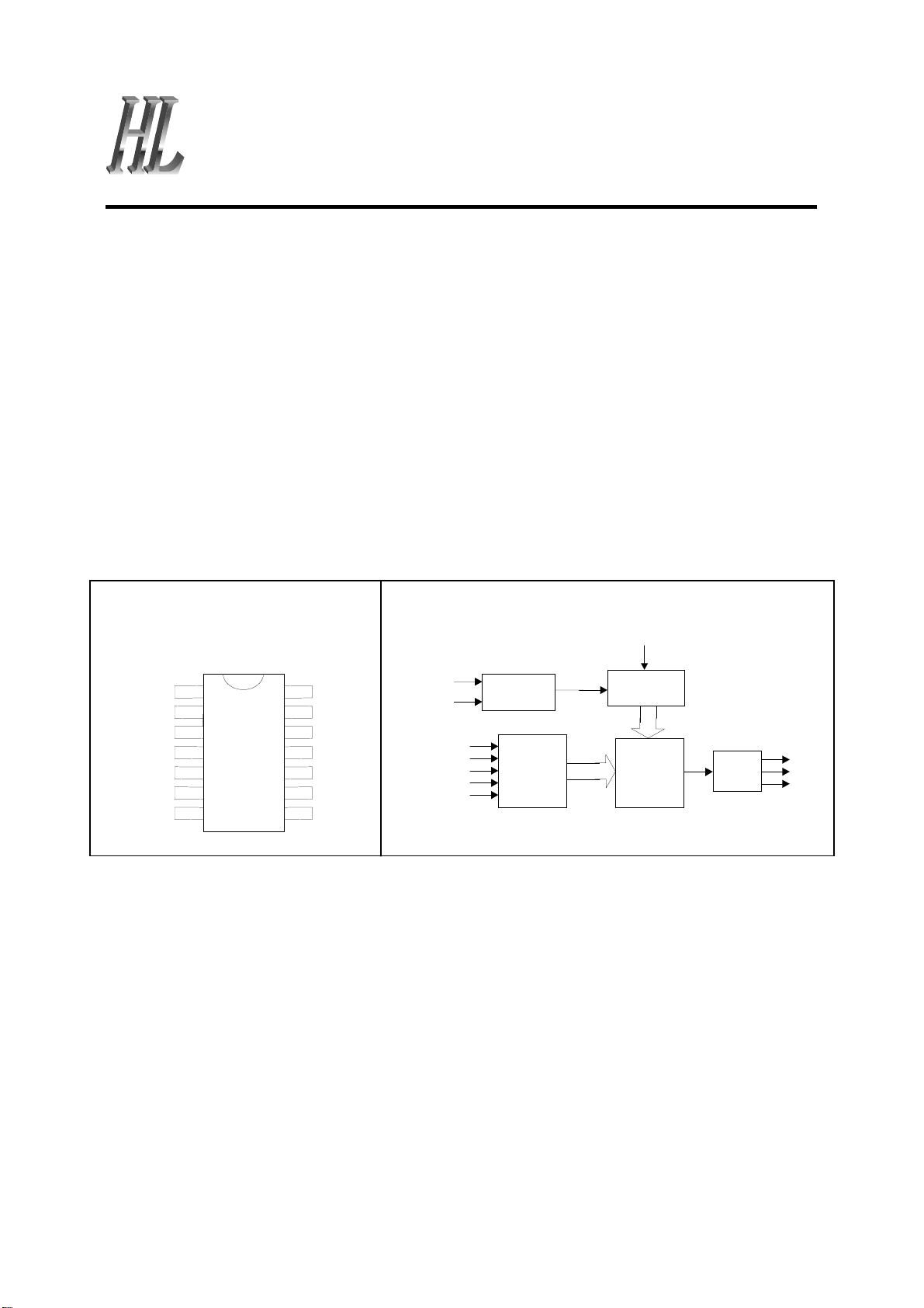
Pin Assignment and Block D iagram:
Transmitter
Pin Assignment
Block Diagram
TESTB
TX2C
RIGHTB
TESTB
GND
BACKWARDB
FORWARDB
TURBOB
SC
1
2
3
4
TX2C
5
6
7
14
13
12
11
10
9
8
LEFTB
FOSC
OSCI
OSCO
PC
VDD
SO
OSCI
OSCO
RIGHTB
LEFTB
TURBOB
FORWARDB
BACKWARDB
Oscillator
Latch
Circuit
Timing
Generator
Encoding
Circuit
Logic
PC
SO
SC
2
http://www.hlec.com.cn
深圳市高地电子有限公司
深圳市高地电子有限公司
深圳市高地电子有限公司深圳市高地电子有限公司
EC
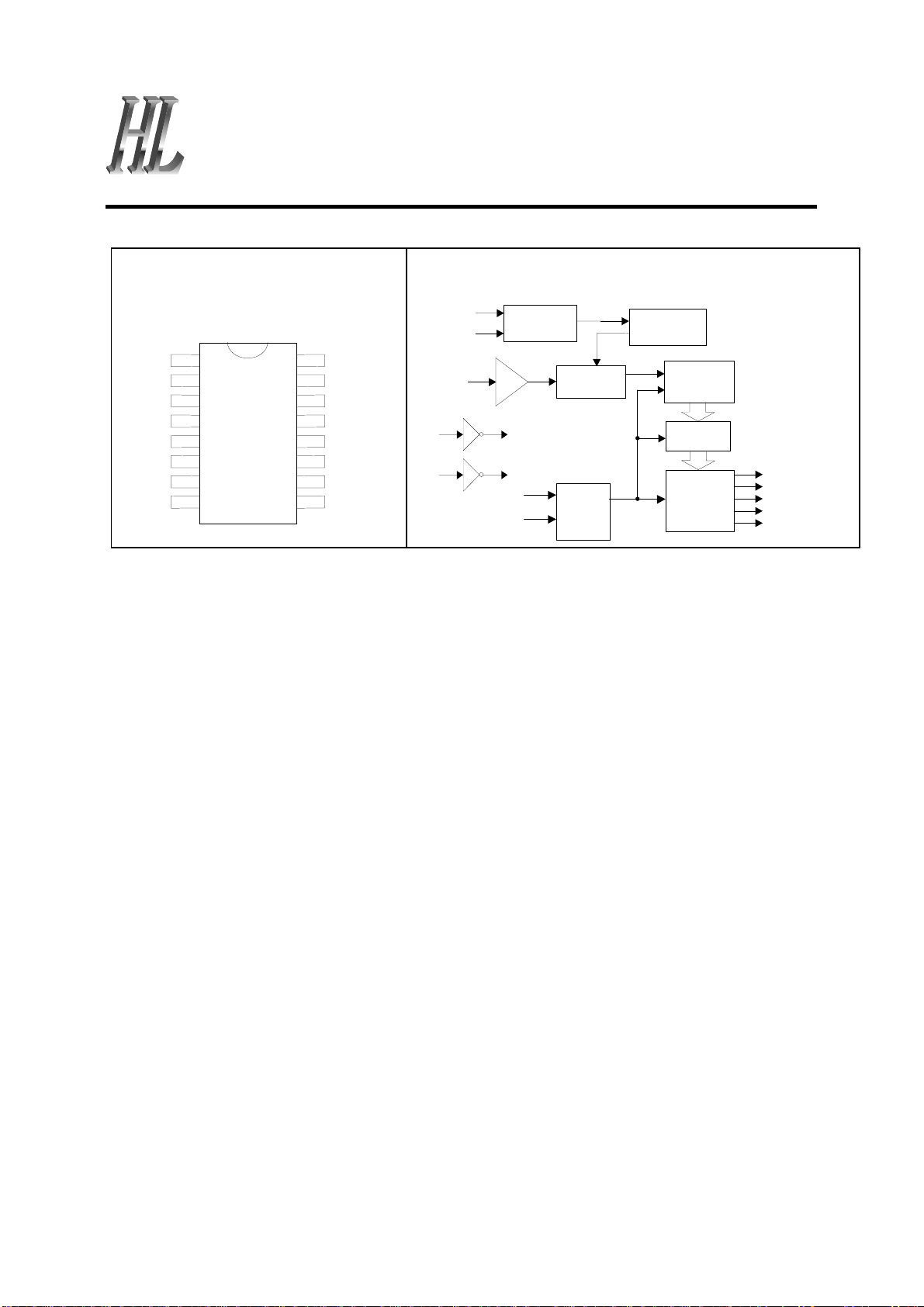
Receiver
Pin Assignment
RX2C
VO2
GND
OSCI
RIGHT
OSCO
LEFT
RDB
SI
1
2
3
4
5
6
7
89
HIGHLAND (SHENZHEN) ELECTRONICS CO., LTD
Block Diagram
RX2C
OSCI
OSCO
16
15
14
13
12
11
10
VI2
VO1
VI1
VDD
TURBO
FORWARD
BACKWARD
LDB
SI
VI1
VI2
AMP
LDB
RDB
Oscillator
VO1
VO2
Decoding
Circuit
Control
Logic
Timing
Generator
Counter
PLA
Latch
TX2/RX2
TX2/RX2
TX2/RX2TX2/RX2
RIGHT
LEFT
TURBO
BACKWARD
FORWARD
Absolute Maximum Ratings
DC Supply Voltage.....................................0.3V to 5.0V
Input/Output Voltage...........GND -0.2V to VDD + 0.2V
Operating temperature..............................-10°C to 60°C
Storage Temperature..............................-25°C to 125°C
Never allow a stress to exceed the values listed under
"Absolute Maximun Ratings", otherwise the device would
suffer from a permanent damage. Nor is a stress at the listed
value be allowed to persist over a period, since an extended
exposure to the absolute maximum rating condition may
also affect the reliability of the device, if not causing a
damage thereof.
Comments*
3
http://www.hlec.com.cn
深圳市高地电子有限公司
深圳市高地电子有限公司
深圳市高地电子有限公司深圳市高地电子有限公司
EC
HIGHLAND (SHENZHEN) ELECTRONICS CO., LTD
TX2/RX2
TX2/RX2
TX2/RX2TX2/RX2
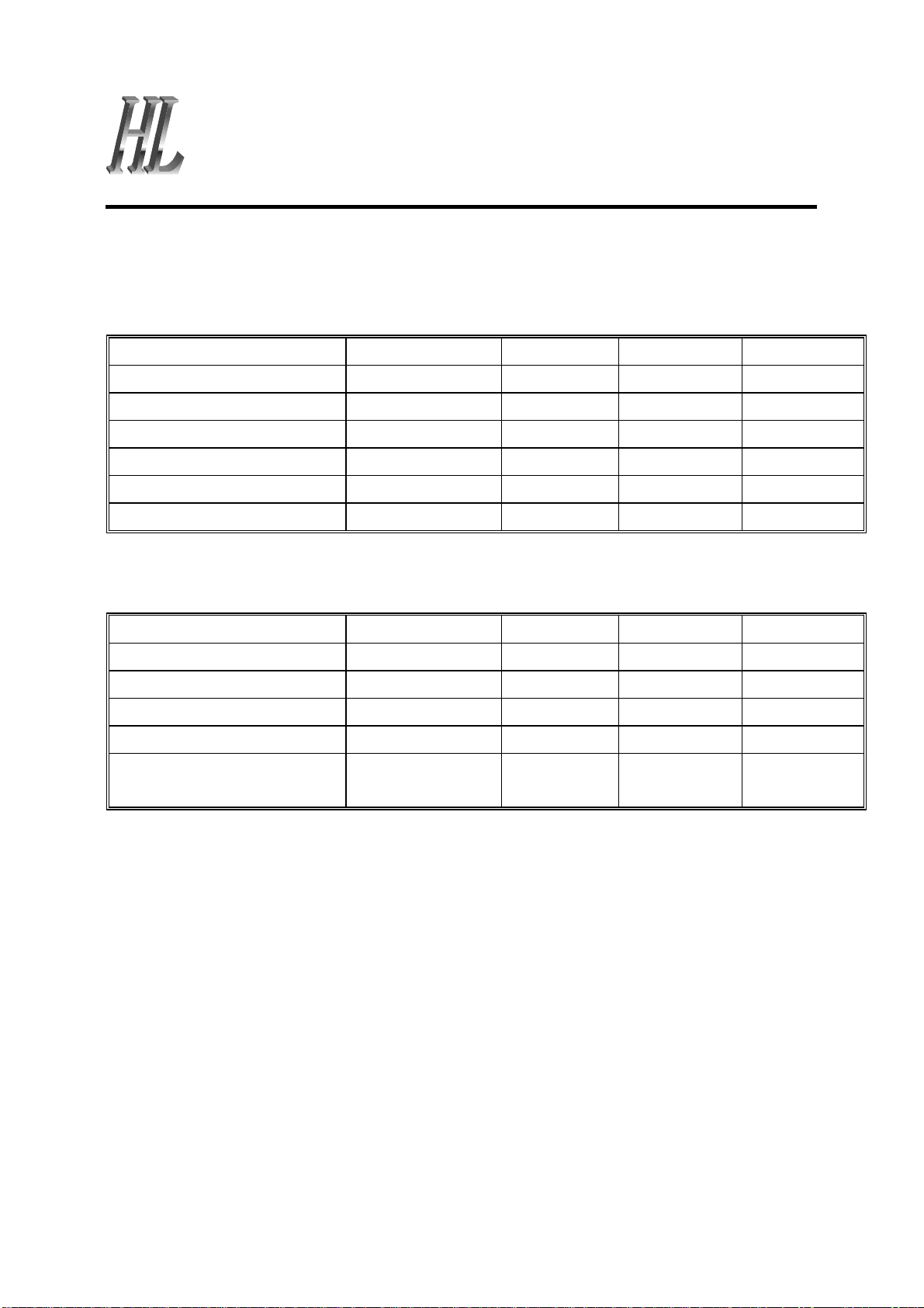
Electrical Characteristics
TX2
(VDD=4.5V, Fosc = 128KHz, TA=25°C, unless otherwise specified.)
Parameter Symbol Min. Typ. Max.
Operating Voltage VDD 2.2V 4.5V 5.0V
Operating Current
Stand-by Current
DC O/P Driving Current
AC O/P Driving Current
AC O/P Frequency
RX2
(VDD=4.5V, Fosc = 128KHz, TA=25°C, unless otherwise specified.)
Idd
I
I
drive
I
drive
F
audio
stb
- - 1mA
- -
3mA - -
3mA - -
500Hz - 1KHz
1µA
Parameter Symbol Min. Typ. Max.
Operating Voltage VDD 2.2V 4.5V 5.0V
Operating Current
O/P Driving Current
O/P Sinking Current
Effect Decoding
Frequency Variation
Idd
I
drive
I
sink
F
tolerance
- - 0.7mA
0.6mA - -
0.6mA - -
-20% - 20%
4
http://www.hlec.com.cn
深圳市高地电子有限公司
深圳市高地电子有限公司
深圳市高地电子有限公司深圳市高地电子有限公司
EC
HIGHLAND (SHENZHEN) ELECTRONICS CO., LTD
TX2/RX2
TX2/RX2
TX2/RX2TX2/RX2
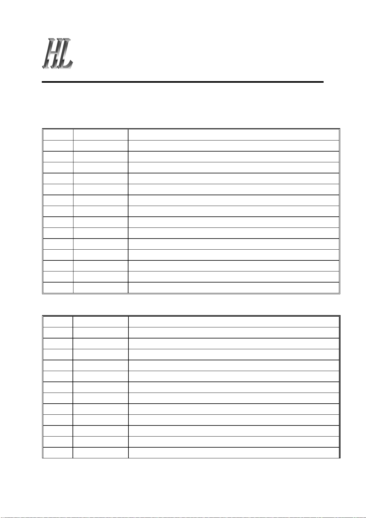
Pin Description
TX2
Pin No. Designation Description
1 RIGHTB The rightward function will be selected when this pin is connected to GND.
2 TESTB This pin is used for testing purpose only.
3 GND Negative power supply
4 BACKWARDB The backward function will be selected when this pin is connected to GND.
5 FORWARDB The forward function will be selected when this pin is connected to GND.
6 TURBOB The turbo function will be selected when this pin is connected to GND.
7 SC Output pin of the encoding signal with carrier frequency
8 SO Output pin of the encoding signal without carrier frequency
9 VDD Positive power supply
10 PC Power control output pin
11 OSCO Oscillator output pin
12 OSCI Oscillator input pin
13 FOSC This pin is used for testing purpose.
14 LEFTB The leftward function will be selected when this pin is connected to GND.
RX2
Pin No. Designation Description
1 VO2 Inverter 2 output pin for power amplify
2 GND Negative power supply
3 SI Input pin of the encoding signal
4 OSCI Oscillator input pin
5 OSCO Oscillator output pin
6 RIGHT Rightward output pin
7 LEFT Leftward output pin
8 RDB Rightward function is disabled when this pin is connected to GND.
9 LDB Leftward function is disabled when this pin is connected to GND.
10 BACKWARD Backward output pin
11 FORWARD Forward output pin
12 TURBO Turbo output pin
5
http://www.hlec.com.cn
 Loading...