

Hittite HMC313 Datasheet
MICROWAVE CORPORATION
HBT BROADBAND AMPLIFIER GAIN BLOCK DC - 6.0 GHz
HMC313
FEBRUARY 2001
Features
P1dB Output Power: +19 dBm
1
Output IP3: +33 dBm
Single Supply: +5V to +7V
High Reliability GaAs HBT Process
AMPLIFIERS
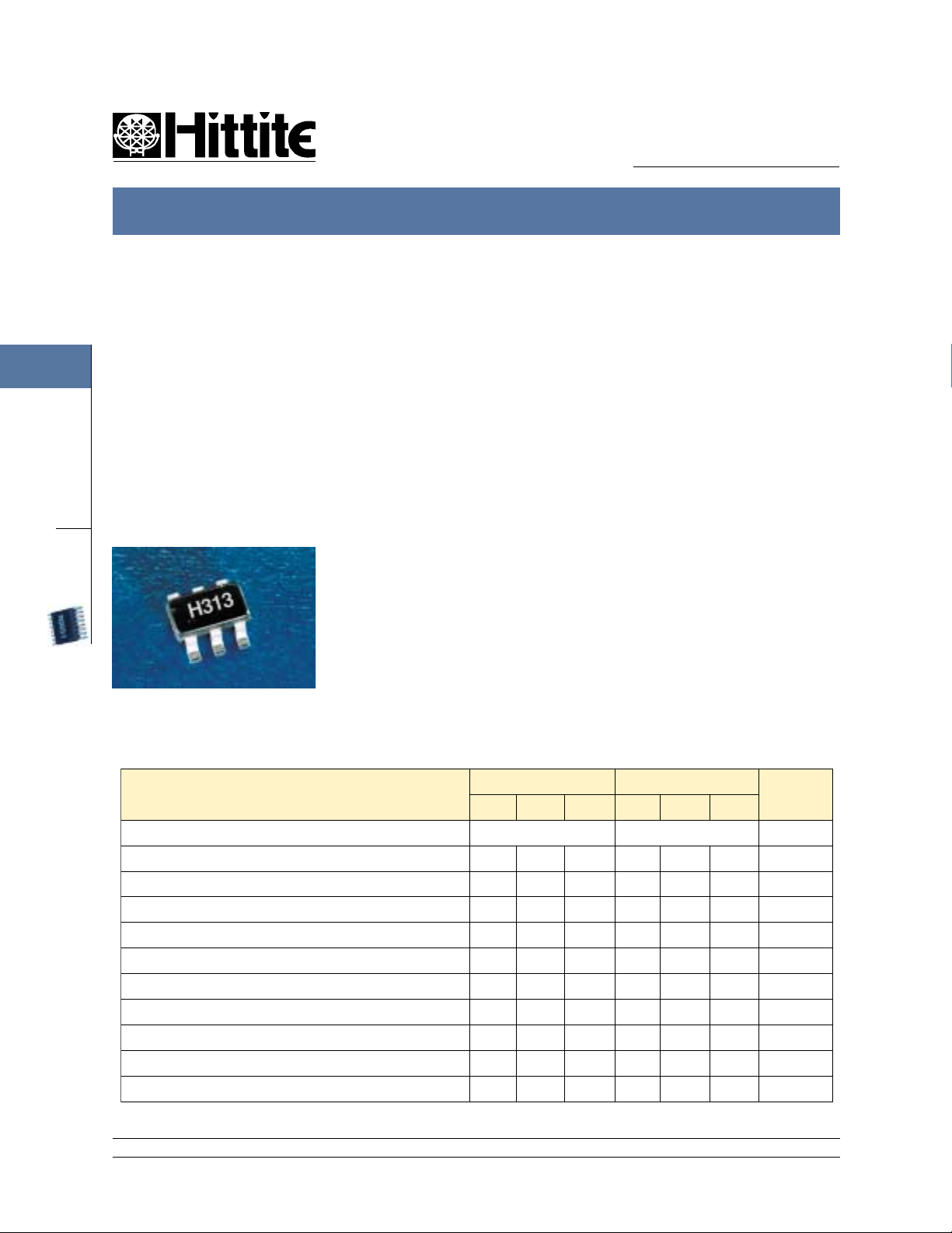
Ultra Small SOT26 Package
SMT
V00.1100
General Description
The HMC313 is a GaAs InGaP Heterojunction
Bipolar Transistor (HBT) MMIC amplifier that
operates from a single Vcc supply. The surface
mount SOT26 amplifier can be used as a broadband gain stage or used with external matching
for optimized narrow band applications. With
Vcc biased at +7V, the HMC313 offers 18 dB of
gain and +20 dBm of saturated power while only
requiring 85 mA of current. The "HMC313 Biasing and Impedance Matching Techniques" application note on page 8-40 offers recommendations for narrow band operation. This amplifier is
ideal as a driver and amplifier for 2.2 - 2.7 GHz
MMDS, 3.5 GHz Wireless Local Loop Applications (WLL), 5.0 - 6.0 GHz UNII and HiperLAN
applications.
Guaranteed Performance, As a Function of Vcc, -40 to +65 deg C
retemaraP
.niM .pyT .xaM .niM .pyT .xaM
egnaRycneuqerF6-CD6-CDzHG
C°52@niaG 317102418112Bd
erutarepmeTrevonoitairaVniaG20.030.020.030.0/BdC°
ssoLnruteRtupnI3737Bd
ssoLnruteRtuptuO2626Bd
noitalosIesreveR62036203Bd
zHG0.1@)Bd1P(noisserpmoCBd1rofrewoPtuptuO11416191mBd
zHG0.1@)tasP(rewoPtuptuOdetarutaS21517102mBd
zHG0.1@)3PI(tpecretnIredrOdrihTtuptuO42720333mBd
erugiFesioN5.652.7Bd
)ccI(tnerruCylppuS0558Am
12 Elizabeth Drive, Chelmsford, MA 01824 Phone: 978-250-3343 Fax: 978-250-3373 Web Site: www.hittite.com
1 - 120
V5+=ccV V7+=ccV
stinU
MICROWAVE CORPORATION
HBT BROADBAND AMPLIFIER GAIN BLOCK DC - 6.0 GHz
HMC313
V00.1100
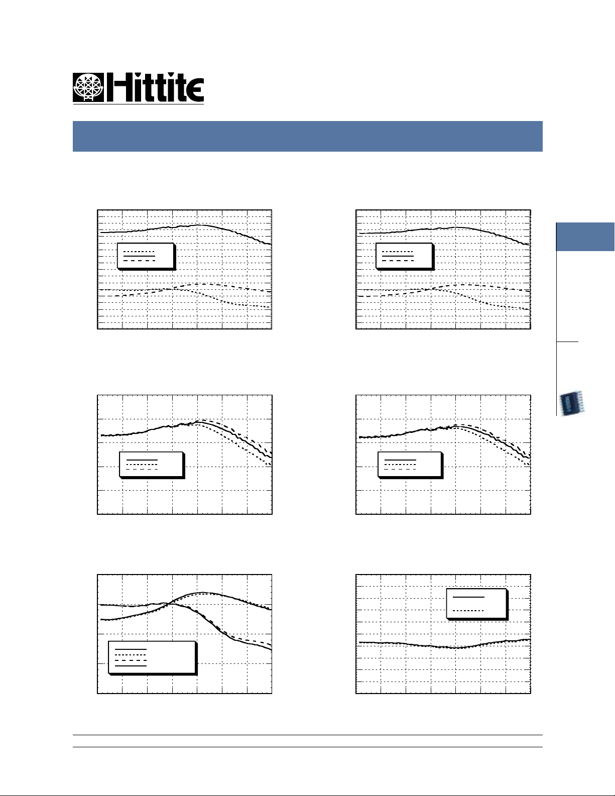
Gain & Return Loss @ Vcc= +7V
25
20
15
10
5
0
-5
RESPONSE (dB)
-10
-15
-20
01234567
S11
S21
S22
FREQUENCY (GHz)
Gain & Return Loss @ Vcc= +5V
25
20
15
10
5
0
-5
RESPONSE (dB)
-10
-15
-20
01234567
S11
S21
S22
FREQUENCY (GHz)
FEBRUARY 2001
Gain vs. Temperature @ Vcc= +7V Gain vs. Temperature @ Vcc= +5V
25
20
15
25
20
15
1
AMPLIFIERS
SMT
+25C
GAIN (dB)
10
5
0
01234567
+85C
-40C
FREQUENCY (GHz)
Input & Output Return Loss vs. Vcc Bias
0
-5
-10
S11 @ Vcc=+5V
RETURN LOSS (dB)
-15
-20
01234567
S22 @ Vcc=+5V
S11 @ Vcc=+7V
S22 @ Vcc=+7V
FREQUENCY (GHz)
GAIN (dB)
10
5
0
01234567
Reverse Isolation vs. Vcc Bias
0
-10
-20
-30
ISOL A T IO N (dB )
-40
-50
01234567
+25C
+85C
-40C
FREQUENCY (GHz)
FREQUENCY (GHz)
+5V
+7V
12 Elizabeth Drive, Chelmsford, MA 01824 Phone: 978-250-3343 Fax: 978-250-3373 Web Site: www.hittite.com
1 - 121
 Loading...