

Hittite HMC282 Datasheet
MICROWAVE CORPORATION
GaAs MMIC LOW NOISE AMPLIFIER 36 - 40 GHz
HMC282
FEBRUARY 2001
1
Features
NOISE FIGURE: 3.5 dB
STABLE GAIN vs. TEMPERATURE: 26dB ± 1.2dB
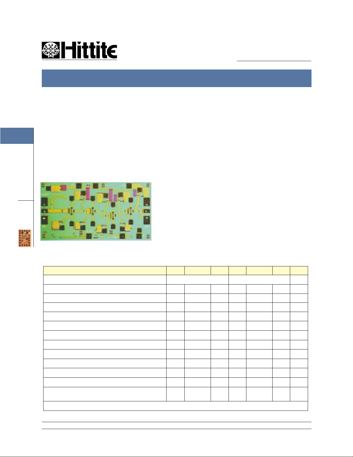
General Description
The HMC282 chip is a four stage GaAs MMIC
Low Noise Amplifier (LNA) which covers the
frequency range of 36 to 40 GHz. The chip can
easily be integrated into Multi-Chip Modules
SMALL SIZE: 1.11 mm x 2.07 mm
(MCMs) due to its small (2.30 mm
chip utilizes a GaAs PHEMT process offering 26
IDEAL FOR 38 GHz RADIOS, E1 & T1
AMPLIFIERS
dB gain from a bias supply of +3.5V @ 90 mA with
a noise figure of 3.5 dB. This LNA can be used in
millimeterwave point-to-point radios, VSAT, and
other SATCOM applications. All data is with the
chip in a 50 ohm test fixture connected via ribbon
DIE
bonds of minimal length. The HMC282 may be
used in conjunction with the HMC259 mixer to
realize a millimeterwave system receiver.
Guaranteed Perf ormance, Vdd = +3.5V*, Idd = 90mA, -55 to +85 deg C
V01.0700
2
) size. The
retemaraP .niM .pyT .xaM .niM .pyT .xaM stinU
egnaRycneuqerF 04-6393-73zHG
niaG12721262Bd
)WBzhG1ynA(ssentalFniaG 1±1±Bd
erugiFesioN 8.38.55.33.5Bd
ssoLnruteRtupnI 76Bd
ssoLnruteRtuptuO 55Bd
noitalosIesreveR04640464Bd
)Bd1P(noisserpmoCBd1rofrewoPtuptuO5959mBd
)tasP(rewoPtuptuOdetarutaS 2121mBd
)3PI(tpecretnIredrOdrihTtuptuO81521272mBd
)ddV(egatloVylppuS52.35.357.352.35.357.3cdV
)4,3gV&2,1gV(egatloVsaiBetaG 3.0-/54.0-3.0-/54.0-cdV
)ddI(tnerruCylppuS
).pyTV51.0-=4,3,2,1gV,V5.3+=ddV(
12 Elizabeth Drive, Chelmsford, MA 01824 Phone: 978-250-3343 Fax: 978-250-3373 Web Site: www.hittite.com
0904109041Am
.lacipytAm09=ddIeveihcaotV4.0+ot0.2-neewteb4,3gV&2,1gVtsujda,V5.3+=ddV*
1 - 60
MICROWAVE CORPORATION
HMC282 LOW NOISE AMPLIFIER 36 - 40 GHz
HMC282
V01.0700
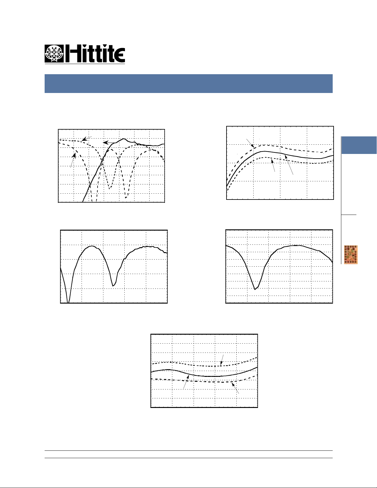
Broadband Gain & Return Loss
35
30
25
20
15
(S11)
GAIN (dB)
10
5
0
-5
26 28 30 32 34 36 38 40
(S22)
FREQUENCY (GHz)
Input Match (S11)
0
-5
-10
-15
-20
INPUT RETURN LOSS (dB)
-25
30 32 34 36 38 40
FREQUENCY (GHz)
Noise Figure vs. Temperature
8
7
6
5
4
3
NOISE FIGURE (dB)
2
1
0
35 36 37 38 39 40
0
-5
-10
-15
-20
RETURN LOSS (dB)
+25 C
FREQUENCY (GHz)
FEBRUARY 2001
Gain vs. Temperature
35
-55 C
30
25
GAIN (dB)
20
+85 C
15
32 34 36 38 40
FREQUENCY (GHz)
+25 C
Output Match (S22)
0
-2
-4
-6
-8
-10
-12
-14
-16
OUTPUT RETURN LOSS (dB)
-18
-20
30 32 34 36 38 40
FREQUENCY (GHz)
+85 C
-55 C
1
AMPLIFIERS
DIE
All data is with the chip in a 50 ohm test fixture connected via ribbon bonds of minimal length.
12 Elizabeth Drive, Chelmsford, MA 01824 Phone: 978-250-3343 Fax: 978-250-3373 Web Site: www.hittite.com
1 - 61
 Loading...