

hittite HMC210MS8 User Manual
查询HMC210MS8供应商
9
MICROWAVE CORPORATION
Typical Applications
The HMC210MS8 is ideal for:
• Base Station Infrastructure
• Portable Wireless
• MMDS
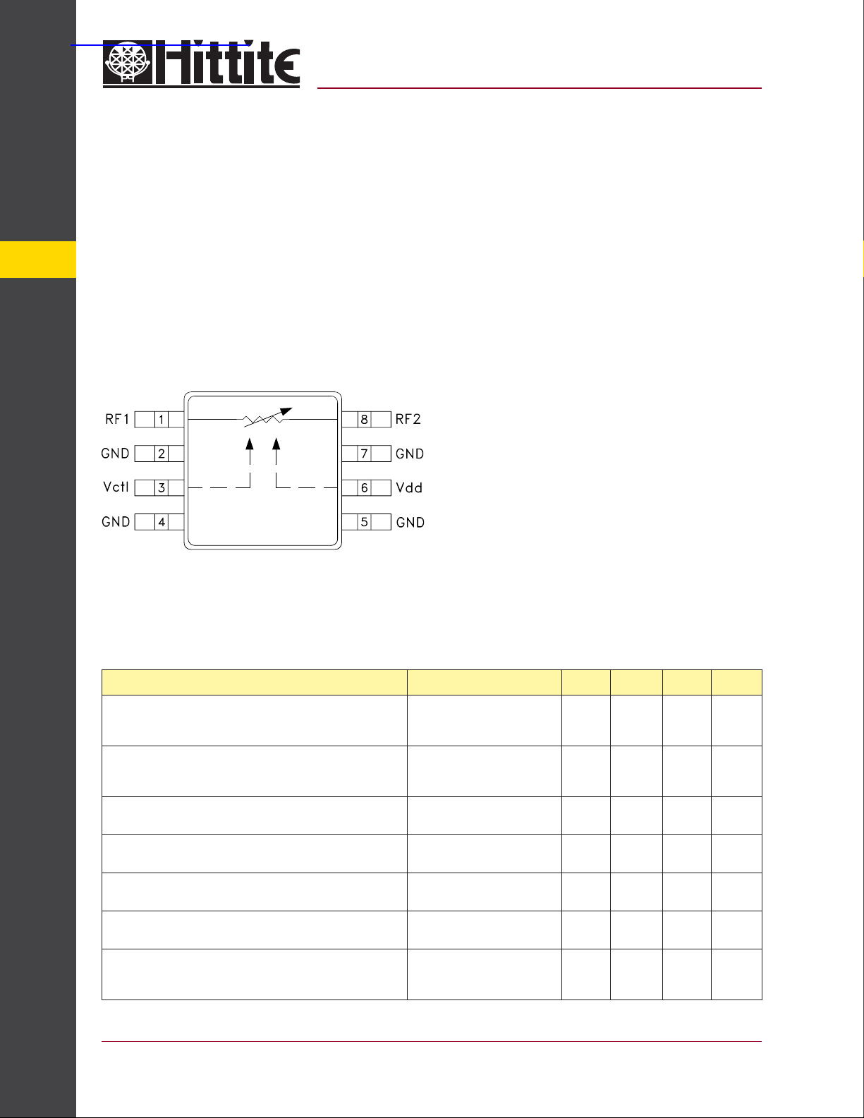
Functional Diagram
v01.0801
HMC210MS8
GaAs MMIC VOLTAGE-VARIABLE
ATTENUATOR, 1.5 - 2.3 GHz
Features
Single Positive Voltage Control: 0 to +2.5V
High Attenuation Range: >50 dB @ 1.9 GHz
High Input IP3: +15 dBm Typical
(All Attenuation States)
Ultra Small Package: MSOP
General Description
The HMC210MS8 is a miniature absorptive voltage
variable attenuator in an 8-lead MSOP package.
The device operates with a positive supply voltage
(+2.5V), and a positive control voltage. A unique
feature is the high third order intercept point for all
attenuation states. Operation up to 2.3 GHz is possible with a reduced attenuation range of 31 dB.
ATTENUATORS - SMT
Electrical Specifi cations, T
Insertion Loss
(VCTL = 0 V Min. Atten.)
Attenuation Range
(VCTL = 0 to +2.5 V)
Return Loss
(VCTL = 0 to +2.5 V)
Input Power for 0.1 dB Compression
(f = 1.9 GHz)
Input Power for 1.0 dB Compression
(f = 1.9 GHz)
Input Third Order Intercept
(f = 1.9 GHz, Two-tone Input Power = +5 dBm Each Tone)
Switching Characteristics
tRISE, tFALL (10/90% RF)
tON, tOFF (50% CTL to 10/90% RF)
= +25° C, Vdd = +2.5 Vdc, 50 Ohm System
A
Parameter Condition Min. Typical Max. Units
1.8 - 2.0 GHz
1.7 - 2.1 GHz
1.5 - 2.3 GHz
1.8 - 2.0 GHz
1.7 - 2.1 GHz
1.5 - 2.3 GHz
1.5 - 2.0 GHz
2.0 - 2.3 GHz
Min Atten.
Atten. >2.0
Min Atten.
Atten. >2.0
Min Atten.
Atten. >2.0
1.5 - 2.3 GHz 0.9
44
39
31
17
0
30
10
3.3
3.4
5.0
55
43
40
15
20
35
15
2.6
4.9
5.5
7.5
9
6
-5
3
dB
dB
dB
dB
dB
dB
dB
dB
dBm
dBm
dBm
dBm
dBm
dBm
µS
µS
9 - 2
For price, delivery, and to place orders, please contact Hittite Microwave Corporation:
12 Elizabeth Drive, Chelmsford, MA 01824 Phone: 978-250-3343 Fax: 978-250-3373
Order Online at www.hittite.com
MICROWAVE CORPORATION
v01.0801
HMC210MS8
GaAs MMIC VOLTAGE-VARIABLE
ATTENUATOR, 1.5 - 2.3 GHz
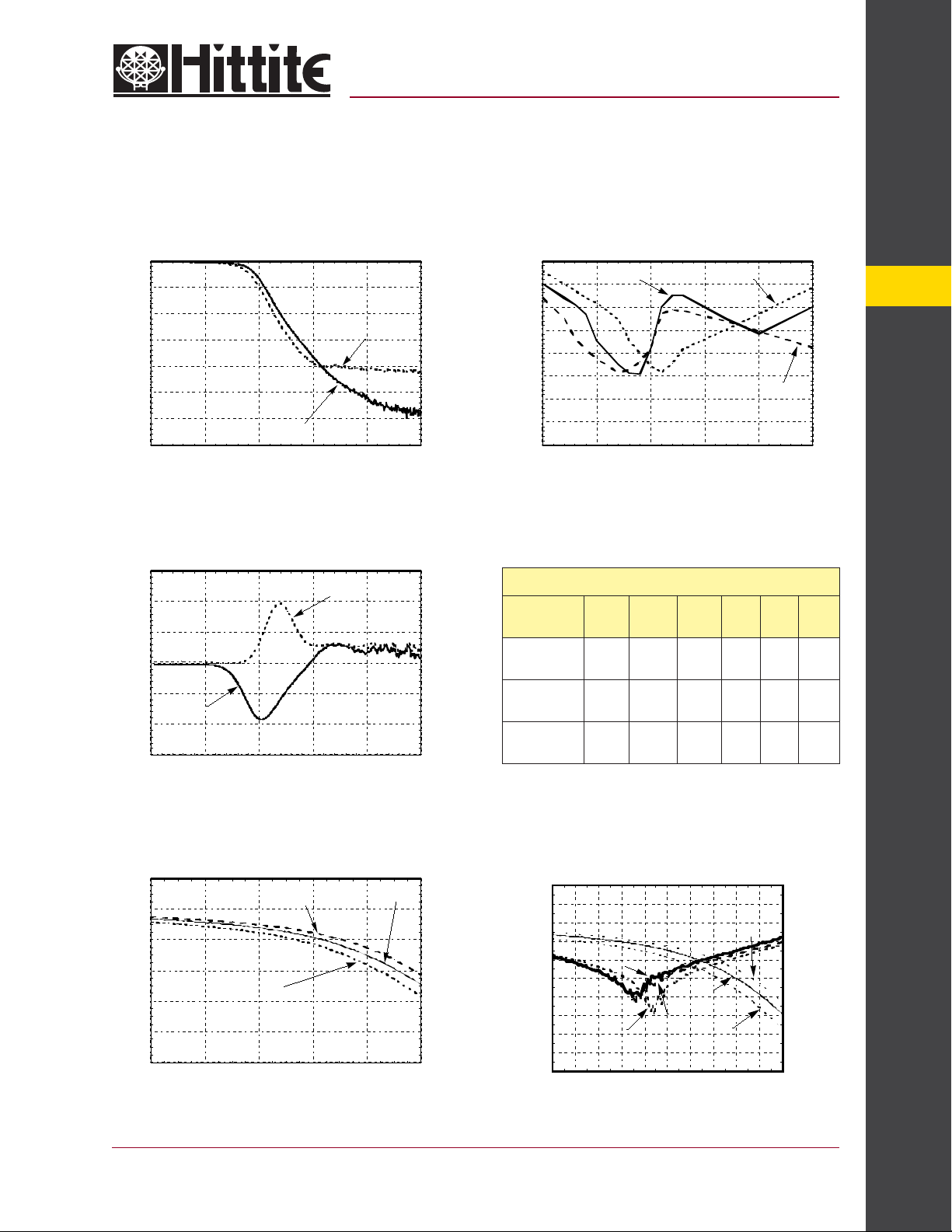
Relative Attenuation vs.
Control Voltage @ 1.9 and 2.2 GHz
0
-10
-20
-30
-40
-50
-60
RELATIVE ATTENUATION (dB)
-70
0 0.5 1 1.5 2 2.5
f= 1.9 GHz
CONTROL VOLTAGE (V)
f= 2.2GHz
Attenuation vs. Temperature
Normalized to +25° C @ 1.9 GHz
15
10
5
0
-5
+85 C
-10
NORMALIZED ATTENUATION (dB)
-15
0 0.5 1 1.5 2 2.5
CONTROL VOLTAGE (V)
-40 C
Input IP3 vs.
Control Voltage @ 1.9 GHz
40
35
30
25
20
15
INPUT IP3 (dBm)
10
5
0
0 0.5 1 1.5 2 2.5
+25 C
CONTROL VOLTAGE (V)
-40 C
Typical Input P1dB Compression
@ 1.9 GHz vs. Temperature
Input Power for 1 dB Compression Point
Test Condition
(1.9 GHz)
Min.
Attenuation
Max.
Attenuation
Worst Case
P1dB
VCTL
(Vdc)
+2.5 +2.5 19 16 25 dBm
+1.0 +2.5 3 4 3 dBm
Vdd
+25C +85C -40C Units
(Vdc)
0.0 +2.5 20 20 21 dBm
9
+85 C
ATTENUATORS - SMT
Broadband Insertion Loss
0
-2
-4
-6
-8
INSERTION LOSS (dB)
-10
-12
1.5 1.7 1.9 2.1 2.3 2.5
FREQUENCY (GHz)
For price, delivery, and to place orders, please contact Hittite Microwave Corporation:
12 Elizabeth Drive, Chelmsford, MA 01824 Phone: 978-250-3343 Fax: 978-250-3373
-40 C
+85 C
Broadband Maximum Relative
Attenuation and Return Loss
+25 C
Order Online at www.hittite.com
0
-20
-40
-60
-80
RELATIVE ATTENUATOR (dB)
-100
1.5 1.7 1.9 2.1 2.3 2.5
+85 C
ATTEN.
+25 C
INS. LOSS
-40 C
+25 C
ATTEN.
ATTEN.
FREQUENCY (GHz)
-40 C
INS. LOSS
+85 C
INS. LOSS
0
INSERTION LOSS (dB)
-2
-4
-6
-8
-10
9 - 3
 Loading...