

Hittite HMC210MS8 Datasheet
MICROWAVE CORPORATION
GaAs MMIC VOLTAGE VARIABLE ATTENUATOR 1.5 - 2.3 GHz
FEBRUARY 2001
HMC210MS8
2
ATTENUATORS
SMT
Features
SINGLE POSITIVE VOLTAGE CONTROL: 0 to +2.5V
HIGH ATTENUATION RANGE: >50 dB @ 1.9 GHz
HIGH INPUT IP3: +15 dBm Typical
(All Attenuation States)
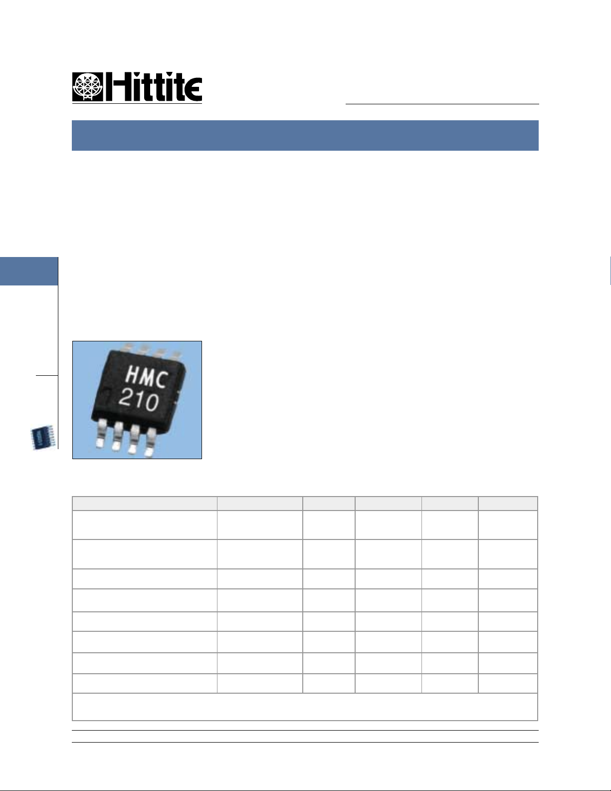
ULTRA SMALL PACKAGE: MSOP
General Description
The HMC210MS8 is a miniature absorptive voltage variable attenuator in an 8lead MSOP package. The device operates with a positive supply voltage (+2.5V),
and a positive control voltage. A unique
feature is the high third order intercept
point for all attenuation states. The
HMC210MS8 is ideal for operation in PCS
applications at 1.9 GHz and W-CDMA
applications through 2.2 GHz. Operation
up to 2.3 GHz is possible, with a reduced
attenuation range of 31 dB.
Guaranteed Performance V
= +2.5 Vdc, 50 Ohm System, -40 to +85°C
dd
Parameter Condition Min Typical Max Units
Insertion Loss
(Vctl = 0 V Min.Atten.)
Attenuation Range
(Vctl=0to+2.5V)
Return Loss
(Vctl=0to+2.5V)
Input Power for 0.1 dB
Compression (f = 1.9 GHz)
Input Power for 1.0 dB
Compression (f = 1.9 GHz))
Input Third Order Intercept
(f = 1.9 GHz, two tones @ +5dBm)
Rise / Fall Time (tRise /tFall)
Note 1
On Time (tOnTotal)
Note 2
Note 1:Ri se T ime(tRise) and Fall Time (tFall) are measured between the 10% and 90% attenuation values.
Note 2:The On Time (tOn Total)is defined as the time fromthe 50% control signal level point to the maximum attenuation
level.
12 Elizabeth Drive, Chelmsford, MA 01824 Phone: 978-250-3343 Fax: 978-250-3373 Web Site: www.hittite.com
1.8 - 2.0 GHz
1.7 - 2.1 GHz
1.5 - 2.3 GHz
1.8 - 2.0 GHz
1.7 - 2.1 GHz
1.5 - 2.3 GHz
1.5 - 2.0 GHz
2.0 - 2.3 GHz
Min.Atten.
Atten.>2.0 dB
Min.Atten.
Atten.>2.0 dB
Min.Atten.
Atten.>2.0 dB
1.5 - 2.3 GHz 0.9 uS
1.5 - 2.3 GHz 2.6 uS
44
39
31
17
0
30
10
3.3
3.4
3.0 - 5.0
55
43
40
9
6
15
-5
20
3
35
15
4.9
5.5
7.5
dB
dB
dB
dB
dB
dB
dB
dB
dBm
dBm
dBm
dBm
dBm
dBm
2 - 32
HMC210MS8
MICROWAVE CORPORATION
HMC210MS8 VOLTAGE VARIABLE ATTENUATOR 1.5 - 2.3 GHz
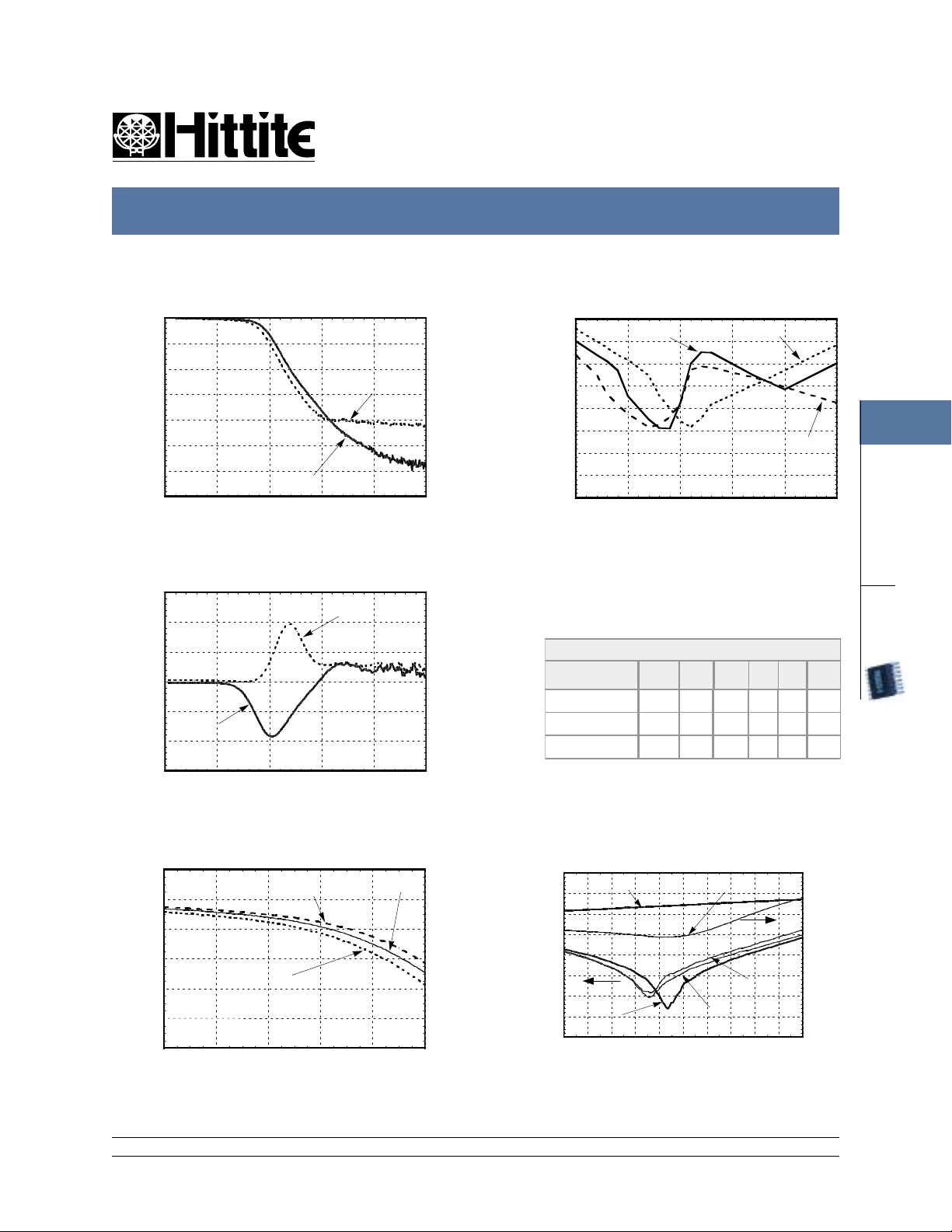
Relative Attenuation vs. Control
Voltage@1.9 and 2.2 GHz
0
-10
-20
-30
-40
-50
-60
RELATIVE ATTENUATION (dB)
-70
0 0.5 1 1.5 2 2.5
f= 1.9 GHz
CONTROL VOLTAGE (V)
f= 2.2GHz
Attenuation vs. Temperature
Normalized to +25°C @1.9 GHz
15
10
5
0
-5
+85 C
-10
NORMALIZED ATTENUATION (dB)
-15
0 0.5 1 1.5 2 2.5
CONTROL VOLTAGE (V)
-40 C
Broadband Insertion Loss
0
-2
-4
-6
-8
INSERTION LOSS (dB)
-10
-12
1.5 1.7 1.9 2.1 2.3 2.5
FREQUENCY (GHz)
-40 C
+85 C
+25 C
Input IP3 vs. Control Voltage
@1.9 GHz
40
35
30
25
20
15
INPUT IP3 (dBm)
10
5
0
0 0.5 1 1.5 2 2.5
+25 C
CONTROL VOLTAGE (V)
Typical Input P1dB Compression
@1.9 GHz vs. Temperature
Input Power For 1 dB Compression Point
Test Condition
(1.9 GHz)
Min. Attenuation 0.0 +2.5 20 20 21 dBm
Max.Attenuation +2.5 +2.5 19 16 25 dBm
WorstCase P1dB +1.0 +2.5 3 4 3 dBm
V
CTL
(Vdc)
Vdd
(Vdc)
Broadband Maximum Relative
Attenuation and Return Loss
0
Vctl = +2.5 V
+25 C
ATTEN.
1.5 1.7 1.9 2.1 2.3 2.5
FREQUENCY (GHz)
RELATIVE ATTENUATION (dB)
-10
-20
-30
-40
-50
-60
-70
-80
FEBRUARY 2001
-40 C
+85 C
+25C +85C -40C Units
Vctl = 0 V
+85 C ATTEN
-40 C
ATTEN.
0
-5
-10
-15
-20
-25
-30
-35
-40
2
ATTENUATORS
SMT
RETURN LOSS (dB)
S - Parameter data is available On-Line at www.hittite.com
12 Elizabeth Drive, Chelmsford, MA 01824 Phone: 978-250-3343 Fax: 978-250-3373 Web Site: www.hittite.com
2 - 33
 Loading...