

Hittite HMC199MS8 Datasheet
'99
new!
MICROWAVE CORPORATION
HMC199MS8 MSOP8 DUAL SPDT SWITCH DC - 2.5 GHz
HMC199MS8
7
FEBRUARY 2001
Features
INTEGRATED DUAL SPDTs
LOW INSERTION LOSS: <0.5 dB @ 2.0 GHz
POSITIVE CONTROL: 0/+5V
ULTRA SMALL MSOP8 PACKAGE: 14.8 mm
V01.0700
General Description
The HMC199MS8 is a low-cost dual SPDT
GaAs “bypass” switch in an 8-lead MSOP
package covering DC to 2.5 GHz. This
four RF port component integrates two
SPDT switches and a through line onto a
2
single IC. The design provides low insertion loss of less than 0.5 dB while switching passive or active external circuit components in and out of the signal path. Port
to port isolations are typically 35 to 20 dB.
On-chip circuitry enables positive voltage
control operation at very low DC currents
with control inputs compatible with CMOS
and most TTL logic families. Applications
include LNA or filter bypass switching and
single bit attenuator switching for cellular,
PCS, and ISM base stations.
Guaranteed Performance Vctl = 0/ +5 Vdc, 50 Ohm System, -40 to +85 deg. C
SWITCHES
Insertion Loss
SPDT
Isolation
Return Loss (On State, Any P ort) DC - 2.0 GHz
Input Power for 1dB Compression 0.5 - 2.0 GHz 19 23 dBm
SMT
Input ThirdOrderIntercept
(Two Tone I nput Power= 0 dBm Each Tone)
Switching Characteristics
tRISE / tFALL (10/90% RF / 90/10% RF)
tON / tOFF (50% CTL to 10/90% RF)
12 Elizabeth Drive, Chelmsford, MA 01824 Phone: 978-250-3343 Fax: 978-250-3373 Web Site: www.hittite.com
7 - 70
Parameter Frequency Min. Typ. Max. Units
DC - 1.0 GHz
DC - 2.0 GHz
DC - 2.5 GHz
DC - 2.0 GHz
DC - 2.5 GHz
DC - 2.5 GHz
0.5 - 2.0 GHz 32 36 dBm
DC - 2. 5 GHz
22
17
22
14
0.3
0.5
0.7
25
21
25
17
20
40
0.6
0.8
1.0
dB
dB
dB
dB
dB
dB
dB
nS
nS
MICROWAVE CORPORATION
HMC199MS8 MSOP8 DUAL SPDT SWITCH DC - 2.5 GHz
H MC199MS8
'99
new!
V01.0700
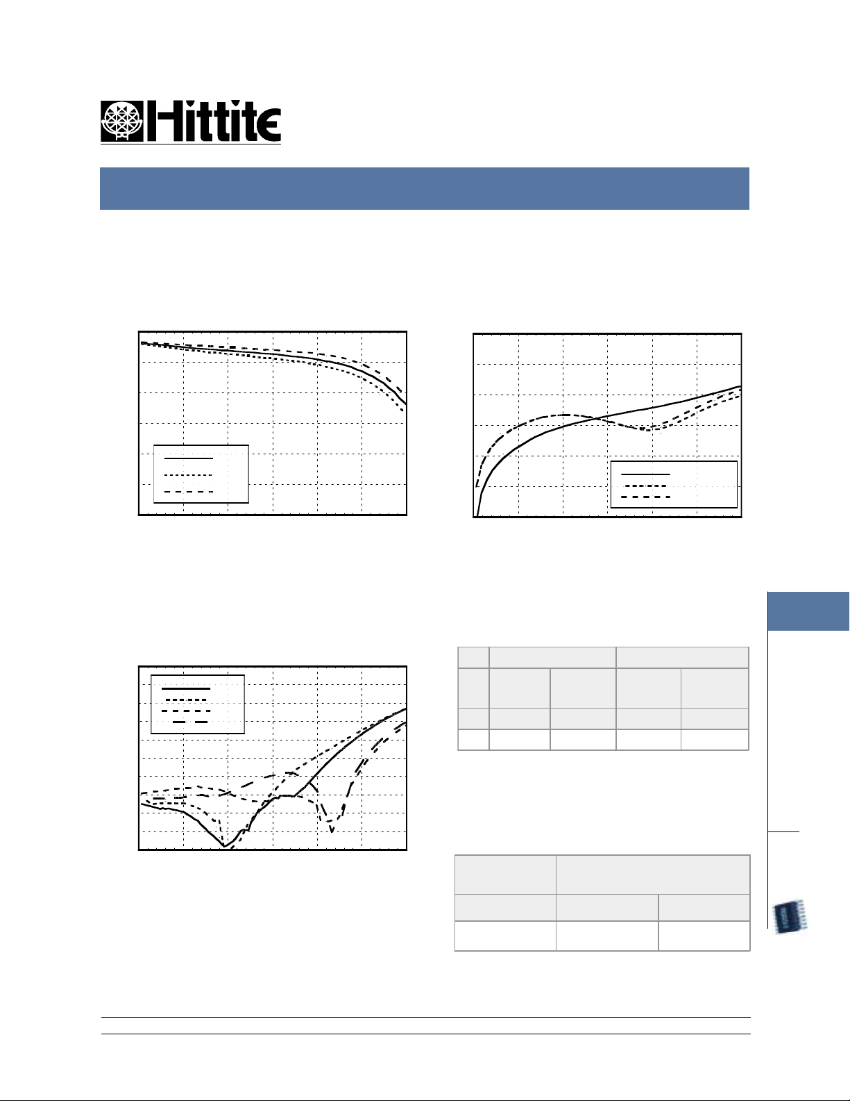
Insertion Loss
0
-0.5
-1
-1.5
-2
INSERTION LOSS (dB)
-2.5
-3
0 0.5 1 1.5 2 2.5 3
+25 C
+85 C
-40 C
FREQUENCY (GHz)
Return Loss
0
-5
-10
-15
-20
-25
-30
-35
RETURN LOSS (dB)
-40
-45
-50
0 0.5 1 1.5 2 2.5 3
RFC1
RFC2
RF1
RF2
FREQUENCY (GHz)
FEBRUARY 2001
Isolation
0
-10
-20
-30
-40
ISOLATION (dB)
RFC1 to RFC2
-50
-60
0 0.5 1 1.5 2 2.5 3
FREQUENCY (GHz)
RFC1 to RF1
RFC2 to RF2
Note: Isolation between RF1 - RF2 ( when RFC1 RFC2 is in insertion loss state) is 25 dB @ 1 GHz
and 17 dB @ 2 GHz.
Compression vs Frequency
Carrier at 900MHz Carrier at 1900MHz
InputPower
CTL
for 0.1dB
Input
Compression
(Vdc) (dBm) (dBm) (dBm) (dBm)
+5 20 23.5 19 22
InputPower
for 1dB
Compression
InputPower
for 0.1dB
Compression
InputPower
Compression
Caution: Do not operate continuously at RF power
input greater than 1dB compression and do not "hot
switch" power levels greater than +13 dBm
(Control =0/ +5Vdc).
Distortion vs Frequency
Control Input
Input Third Order Intercept (dBm)
0 dBm Each Tone
7
for 1dB
SWITCHES
SPDT
SMT
(Vdc) 900 MHz 1900 MHz
+5 34.5 37.5
12 Elizabeth Drive, Chelmsford, MA 01824 Phone: 978-250-3343 Fax: 978-250-3373 Web Site: www.hittite.com
7 - 71
 Loading...