

查询HMC174MS8供应商
14
MICROWAVE CORPORATION
Typical Applications
The HMC174MS8 is ideal for:
• ISM Applications
• PCMCIA Wireless Cards
• Portable Wireless
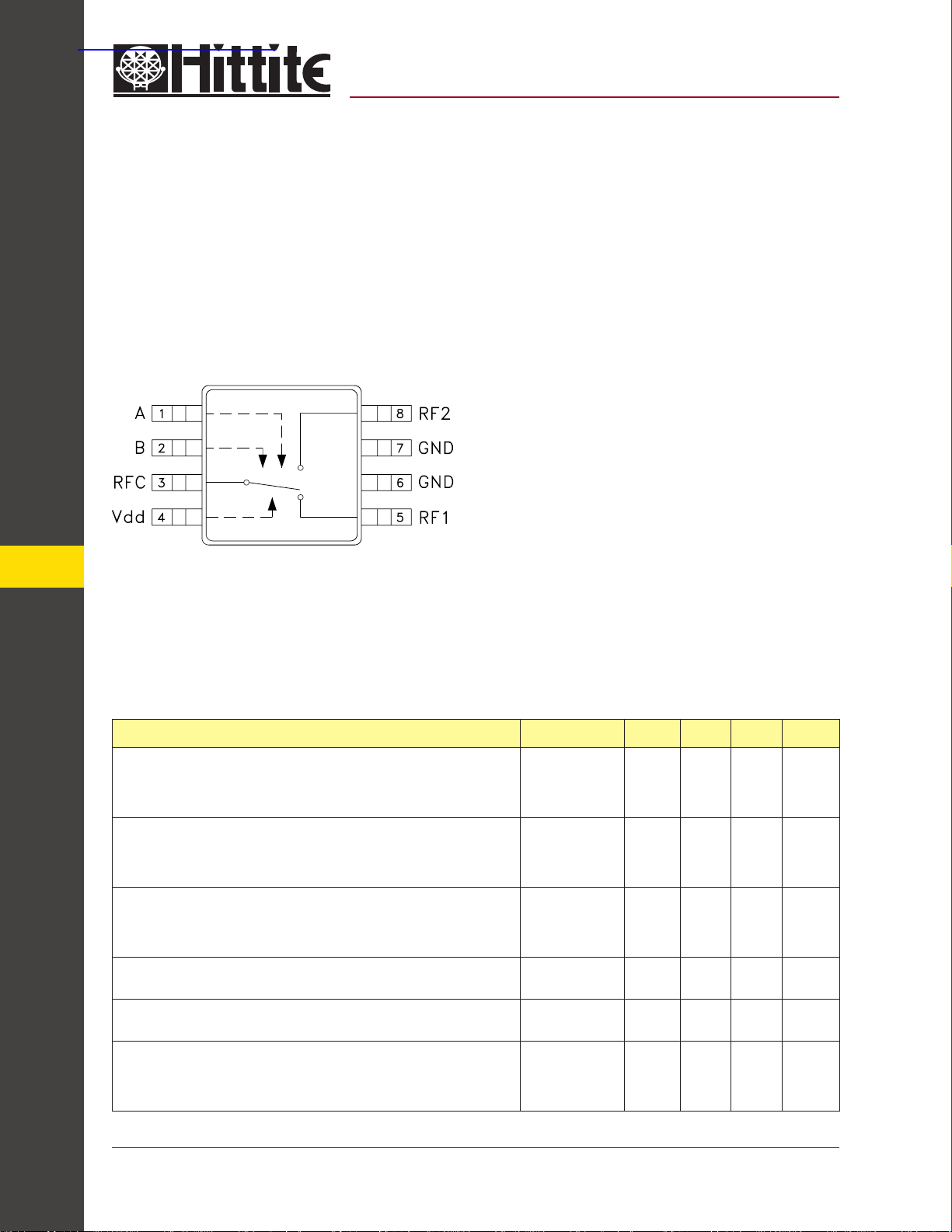
Functional Diagram
v01.0101
HMC174MS8
GaAs MMIC T/R SWITCH
DC - 3 GHz
Features
Ultra Small Package: MSOP8
High Third Order Intercept: +60 dBm
Single Positive Supply: +3 to +10V
High RF power Capabilty
General Description
The HMC174MS8 is a low-cost SPDT switch in
an 8-lead MSOP package for use in transmitreceive applications which require very low distortion at high signal power levels. The device
can control signals from DC to 3.0 GHz and is
especially suited for 900 MHz, 1.8 - 2.2 GHz, and
2.4 GHz ISM applications with only 0.5 dB loss.
The design provides exceptional intermodulation
performance; providing a +60 dBm third order
intercept at 8 Volt bias. RF1 and RF2 are refl ective shorts when “OFF”. On-chip circuitry allows
single positive supply operation at very low DC
current with control inputs compatible with CMOS
and most TTL logic families.
Electrical Specifi cations, T
Insertion Loss
Isolation
SWITCHES - SMT
Return Loss
Input Power for 1dB Compression 0/8V Control
Input Third Order Intercept 0/8V Control
Switching Characteristics DC - 3.0 GHz
= +25° C, Vdd = +5 Vdc, 50 Ohm System
A
Parameter Frequency Min. Typ. Max. Units
tON, tOFF (50% CTL to 10/90% RF)
tRISE, tFALL (10/90% RF)
DC - 1.0 GHz
DC - 2.0 GHz
DC - 2.5 GHz
DC - 3.0 GHz
DC - 1.0 GHz
DC - 2.0 GHz
DC - 2.5 GHz
DC - 3.0 GHz
DC - 1.0 GHz
DC - 2.0 GHz
DC - 2.5 GHz
DC - 3.0 GHz
0.5 - 1.0 GHz
0.5 - 3.0 GHz
0.5 - 1.0 GHz
0.5 - 3.0 GHz
22
20
17
13
20
16
13
9
35
34
55
55
0.5
0.5
0.7
1.4
25
24
21
17
28
21
17
11
39
38
60
60
10
24
0.7
0.8
1.0
1.8
dB
dB
dB
dB
dB
dB
dB
dB
dB
dB
dB
dB
dBm
dBm
dBm
dBm
ns
ns
14 - 20
For price, delivery, and to place orders, please contact Hittite Microwave Corporation:
12 Elizabeth Drive, Chelmsford, MA 01824 Phone: 978-250-3343 Fax: 978-250-3373
Order Online at www.hittite.com
MICROWAVE CORPORATION
v01.0101
HMC174MS8
GaAs MMIC T/R SWITCH
DC - 3 GHz
GaAs MMIC SUB-HARMONICALLY PUMPED MIXER 17 - 25 GHz
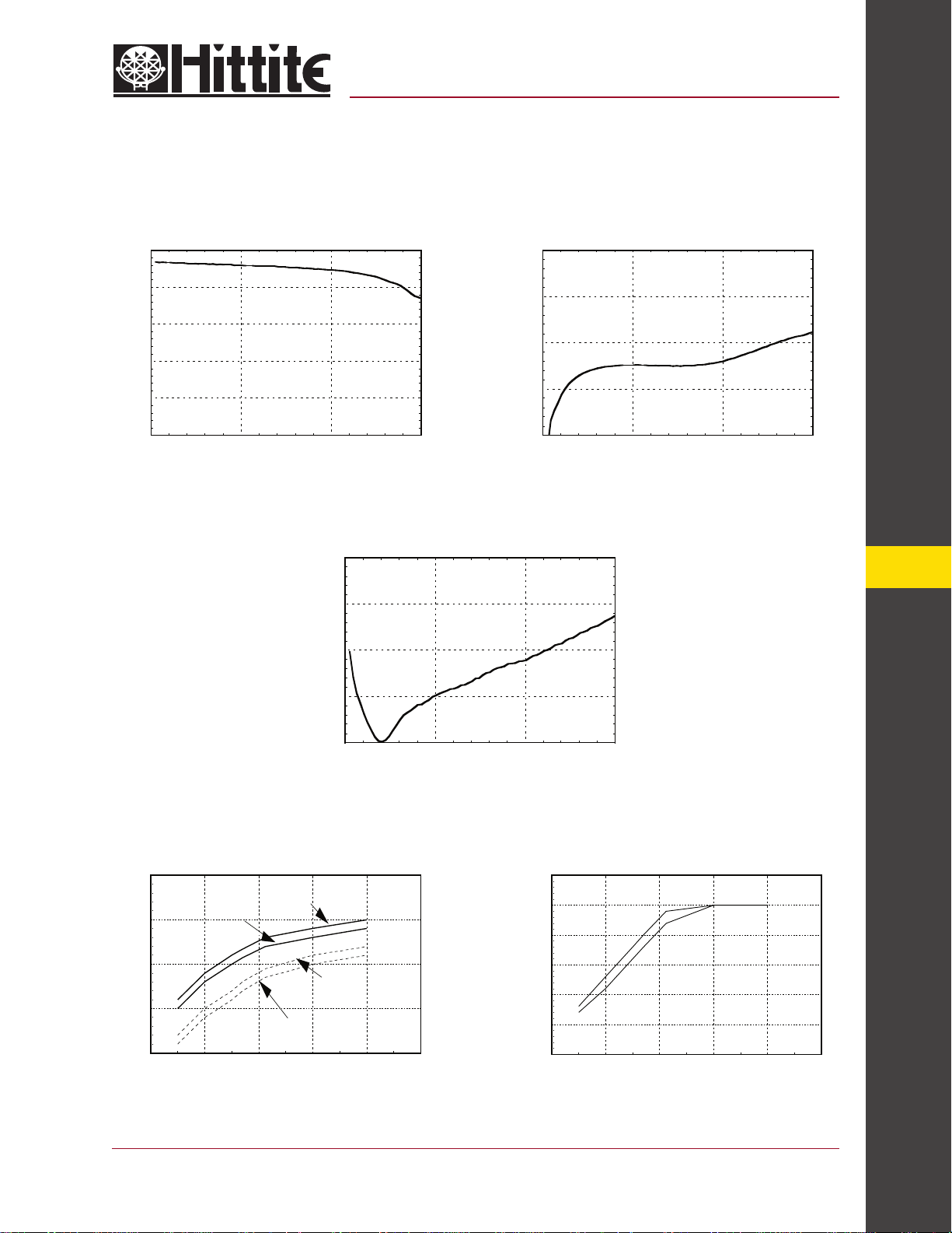
Insertion Loss
0
Isolation
0
-1
-2
-3
INSERTION LOSS (dB)
-4
-5
0123
FREQUENCY (GHz)
Return Loss
0
-10
-20
-30
INPUT RETURN LOSS (dB)
-10
-20
ISOLATION (dB)
-30
-40
0123
FREQUENCY (GHz)
14
-40
0123
Input 0.1 and 1.0 dB
Compression vs. Bias Voltage
45
1db at 1900MHz
40
35
30
COMPRESSION (dBm)
25
2 4 6 8 10 12
For price, delivery, and to place orders, please contact Hittite Microwave Corporation:
12 Elizabeth Drive, Chelmsford, MA 01824 Phone: 978-250-3343 Fax: 978-250-3373
1dB at 900MHz
0.1dB at 900MHz
0.1dB at 1900MHz
BIAS (Volts)
FREQUENCY (GHz)
Input Third Order
Intercept vs. Bias Voltage
65
60
55
50
IP3 (dBm)
45
40
35
2 4 6 8 10 12
Order Online at www.hittite.com
SWITCHES - SMT
900MHz
1900MHz
BIAS (Volts)
14 - 21

MICROWAVE CORPORATION
Carrier at 900 MHz Carrier at 1900 MHz
Input Power
Bias
for 0.1 dB
Vdd
Compression
(Volts) (dBm) (dBm) (dBm) (dBm)
327 31 26 30
430 34 29 33
532 36 31 35
836 39 35 38
10 37 40 36 39
Input Power
for 1.0 dB
Compression
Input Power
for 0.1 dB
Compression
Input Power
for 1.0 dB
Compression
Caution: Do not operate in 1dB compression at power
levels above +35dBm and do not ‘hot switch’ power levels
v01.0101
greater than +23dBm (V
= +5Vdc).
dd
HMC174MS8
GaAs MMIC T/R SWITCH
DC - 3 GHz
Distortion vs. Bias VoltageCompression vs. Bias Voltages
1 Watt Carrier at 900 MHz 1 Watt Carrier at 1900 MHz
Third
Order
Second
Order
Intercept
Second
Harmonic
Bias
Vdd
Intercept
(Volts) (dBm) (dBm) (dBc) (dBm) (dBm) (dBc)
343 71 45 4278 55
448 85 55 4688 65
553 90 56 5187 58
860 90 58 6090 59
10 60 90 59 60 90 60
Third
Order
Intercept
Second
Order
Intercept
Second
Harmonic
14
Truth Table
*Control Input Voltage Tolerances are ± 0.2 Vdc
Bias Control Input*
Vdd
(Vdc)A(Vdc)B(Vdc)
3 0 0 30 -15 -15 OFF OFF
3 0 Vdd 25 -25 0 ON OFF
3 Vdd 0 25 0 -25 OFF ON
5 0 0 110 -55 -55 OFF OFF
5 0 Vdd 115 -100 -15 ON OFF
5 Vdd 0 115 -15 -100 OFF ON
10 0 0 380 -190 -190 OFF OFF
SWITCHES - SMT
10 0 Vdd 495 -275 -220 ON OFF
10 Vdd 0 495 -220 -275 OFF ON
5 -Vdd Vdd 600 -600 225 ON OFF
5 Vdd -Vdd 600 225 -600 OFF ON
Bias
Current
Idd
(uA)
Control
Current
Ia
(uA)
Control
Current
Ib
(uA)
Signal Path State
RF to
RF1
RF to
RF2
14 - 22
For price, delivery, and to place orders, please contact Hittite Microwave Corporation:
12 Elizabeth Drive, Chelmsford, MA 01824 Phone: 978-250-3343 Fax: 978-250-3373
Order Online at www.hittite.com

MICROWAVE CORPORATION
v01.0101
Absolute Maximum Ratings
Bias Voltage Range (Vdd) -0.2 to +12 Vdc
Control Voltage Range (A & B) -0.2 to +Vdd Vdc
Storage Temperature -65 to +150 °C
Operating Temperature -40 to +85 °C
Outline Drawing
HMC174MS8
GaAs MMIC T/R SWITCH
DC - 3 GHz
NOTES:
1. PACKAGE BODY MATERIAL: LOW STRESS INJECTION MOLDED
PLASTIC SILICA AND SILICON IMPREGNATED.
2. LEADFRAME MATERIAL: COPPER ALLOY
3. LEADFRAME PLATING: Sn/Pb SOLDER
4. DIMENSIONS ARE IN INCHES [MILLIMETERS].
5. DIMENSION DOES NOT INCLUDE MOLDFLASH OF 0.15mm PER SIDE.
6. DIMENSION DOES NOT INCLUDE MOLDFLASH OF 0.25mm PER SIDE.
7. ALL GROUND LEADS MUST BE SOLDERED TO PCB RF GROUND.
14
SWITCHES - SMT
For price, delivery, and to place orders, please contact Hittite Microwave Corporation:
12 Elizabeth Drive, Chelmsford, MA 01824 Phone: 978-250-3343 Fax: 978-250-3373
Order Online at www.hittite.com
14 - 23

MICROWAVE CORPORATION
v01.0101
Typical Application Circuit
HMC174MS8
GaAs MMIC T/R SWITCH
DC - 3 GHz
14
Notes:
1. Set logic gate and switch Vdd = +3V to +5V and use HCT series logic to provide a TTL driver interface.
2. Control inputs A/B can be driven directly with CMOS logic (HC) with Vdd of 3 to 8 Volts applied to the CMOS
SWITCHES - SMT
logic gates and to pin 4 of the RF switch.
3. DC Blocking capacitors are required for each RF port as shown. Capacitor value determines
lowest frequency of operation.
4. Highest RF signal power capability is achieved with V set to +10V. The switch will operate properly (but at lower
RF power capability) at bias voltages down to +3V.
14 - 24
For price, delivery, and to place orders, please contact Hittite Microwave Corporation:
12 Elizabeth Drive, Chelmsford, MA 01824 Phone: 978-250-3343 Fax: 978-250-3373
Order Online at www.hittite.com

MICROWAVE CORPORATION
Evaluation Circuit Board
v01.0101
HMC174MS8
GaAs MMIC T/R SWITCH
DC - 3 GHz
List of Material
Item Description
J1 - J3 PC Mount SMA RF Connector
J4 - J7 DC Pin
C1 - C3 100 pF capacitor, 0402 Pkg.
C4 10,000 pF capacitor, 0603 Pkg.
U1 HMC174MS8 T/R Switch
The circuit board used in the fi nal application should
be generated with proper RF circuit design techniques. Signal lines at the RF port should have 50
ohm impedance and the package ground leads and
package bottom should be connected directly to the
ground plane similar to that shown above. The evaluation circuit board shown above is available from Hittite Microwave Corporation upon request.
14
SWITCHES - SMT
PCB* 104122 Evaluation PCB
* Circuit Board Material: Rogers 4350
For price, delivery, and to place orders, please contact Hittite Microwave Corporation:
12 Elizabeth Drive, Chelmsford, MA 01824 Phone: 978-250-3343 Fax: 978-250-3373
Order Online at www.hittite.com
14 - 25
 Loading...