

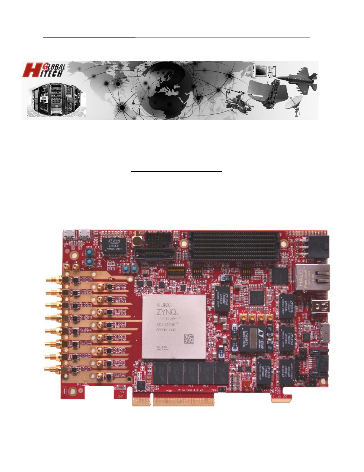
HiTech Global HTG-ZRF8 User Manual
1
HTG-ZRF8 Platform User Manual
HiTech Global ZYNQ UltraScale+™ RFSoC Development Platform
HTG-ZRF8 User Manual
Version 1.0 August 2018
Copyright © HiTech Global 2004-2018
www.HiTechGlobal.com
2
Date
Version
Notes
8/15/2017
1.0
HTG-ZRF8 Platform User Manual
Disclaimer
HiTech Global does not assume any liability arising out of the application or use of any product described or
shown herein; nor does it convey any license under its patents, copyrights, or mask work rights or any rights of
others. HiTech Global reserves the right to make changes, at any time, in order to improve reliability and
functionality of this product. HiTech Global will not assume responsibility for the use of any circuitry described
herein other than circuitry entirely embodied in its products. HiTech Global provides any design, code, or
information shown or described herein "as is." By providing the design, code, or information as one possible
implementation of a feature, application, or standard, HiTech Global makes no representation that such
implementation is free from any claims of infringement. End users are responsible for obtaining any rights they
may require for their implementation. HiTech Global expressly disclaims any warranty whatsoever with respect
to the adequacy of any such implementation, including but not limited to any warranties or representations that
the implementation is free from claims of infringement, as well as any implied warranties of merchantability or
fitness for a particular purpose.
HiTech Global will not assume any liability for the accuracy or correctness of any engineering or software
support or assistance provided to a user. HiTech Global products are not intended for use in life support
appliances, devices, or systems. Use of a HiTech Global product in such applications without the written
consent of the appropriate HiTech Global officer is prohibited.
The contents of this manual are owned and copyrighted by HiTech Global Copyright HiTech Global All Rights
Reserved. Except as stated herein, none of the material may be copied, reproduced, distributed, republished,
downloaded, displayed, posted, or transmitted in any form or by any means including, but not limited to,
electronic, mechanical, photocopying, recording, or otherwise, without the prior written consent of HiTech
Global. Any unauthorized use of any material contained in this manual may violate copyright laws, trademark
laws, the laws of privacy and publicity, and communications regulations and statutes.
Revision History
www.HiTechGlobal.com
3
1.0) Overview
5
2.0) Features
6
3.0) Banks Assignment, Block Diagram, & Clocks
6
4.0) Main Clocks
11
5.0) PCI Express
14
6.0) DDR 4 Memory
17
7.0) FPGA Mezzanine Card (FMC+)
24
8.0) ADC / DAC Ports
30
9.0) USB To UART Bridges
32
10.0) ARM Trace Port
33
11.0) SDIO Interface
34
12.0)10/100/1000 Ethernet
35
13.0) Display Port
36
14.0) USB2.0/3/0
36
15.0) SATA
37
16.0) 1-PPS
37
17.0) LEDs, XDAC, User I/O Headers & Pushbutton
38
18.0) IP Protection
39
19.0) I2C Bus Switch
39
20.0) Configuration
40
Table (1) FPGA Features
5
Table (2): Main Clocks
11
Table (3): Summary of the Si5341 (U46) Clock Outputs
13
Table (4): PCI Express FPGA Pin Assignments
15
Table (5): PCI Express Clock Circuit
16
Table (6): DDR4 FPGA Pin Assignment (SODIMM-PL Side)
20
Table (7) DDR4 FPGA Pin Assignment (Components-PS Side)
24
Table (8): Vita57.4 FMC+ Pin Assignment
25
Table (9): FPGA Mezzanine Connector (FMC+) Pin Assignment
28
Table (10): RFB Resistor Table vs Various Output Voltages
29
Table (11): ADC Interface Pin Assignment
30
Table (12): DAC Interface Pin Assignment
31
Table (13): USB To UART FPGA Pin Assignment
33
Table (14): Trace/Debug Port’s FPGA Pin Assignment
34
HTG-ZRF8 Platform User Manual
Table Of Contents
Tables & Figures
www.HiTechGlobal.com
4
Table (15): SDIO Port’s FPGA Pin Assignment
35
Table (16): Ethernet Port’s FPGA Pin Assignment
35
Table (17): Display Port’s FPGA Pin Assignment
36
Table (18): USB Port’s FPGA Pin Assignment
37
Table (19): SATA Port’s FPGA Pin Assignment
37
Table (20): 1-PPS Port’s FPGA Pin Assignment
38
Table (21): User Interface FPGA Pin Assignment
38
Figure (1): FPGA Bank Assignment
7
Figure (2): System Block Diagram
8
Figure (3): Clock Block Diagram
9
Figure (4): Mechanical Drawing
10
Figure (5): Si5341 Block Diagram
12
Figure (6): LMX2482 Block Diagram
14
Figure (7): PCI Express Clock Circuit
16
Figure (8): PCI Express Clock Enable Circuit
17
Figure (9): HSPC (Vita57.4) Carrier Card Connector Grid Labeling
24
Figure (10): FMC+/FMC VADJ Configurations
29
Figure (11): ADC/DAC Clock Diagram
32
Figure (12): I2C Bus Switch
40
Figure (13): Configuration Option
41
HTG-ZRF8 Platform User Manual
www.HiTechGlobal.com
5
HTG-ZRF8 Platform User Manual
◙ 1.0) Overview
Populated with one Xilinx ZYNQ UltraScale+ RFSoC ZU25DR, ZU27DR, or ZU28DR, the HTG-ZRF8
provides access to large FPGA gate densities, multiple ADC/DAC ports, expandable I/Os ports and DDR4
memory for variety of different programmable applications.
The HTG-ZRF8 is supported by eight 12-bit ADC (4GSPS) and eight 14-bit DAC (6.4GSPS) ports. The ADC
and DAC ports are supported through high-performance front panel micro Rf connectors.
The HTG-ZRF8 architecture allows easy and versatile functional expansion through one Vita 57.4 compliant
(FMC+) port. The HTG-ZRF8 can host wide range of Vita57.1 /Vita57.4 compliant daughter cards.
The HTG-ZRF8 is supported by one 72-bit ECC DDR4 SODIMM socket providing access to up to 16 GB of
SDRAM memory. The processor’s side is supported by up to 2GB of DDR4 memory.
The HTG-ZRF8 can be used in PCI Express and Standalone mode and powered through its 6-pin Molex PCIe
connector.
Table (1) illustrates key features of the supported FPGAs by the HTG-ZRF8 platform.
Table (1): Summary of supported ZYNQ RFSoc UltraScale+ FPGA Features
www.HiTechGlobal.com

6
HTG-ZRF8 Platform User Manual
◙ 2.0) HTG-ZRF8 Platform’s Features
►Xilinx Zynq UltraScale+ RFSoc ZU25DR, ZU27DR, or ZU28DR
►x8 ADC (12-bit , 4GSPS) ports (SMCC connectors)
►x8 DAC (14-bit, 6.4GSPS) ports (SMCC connectors)
►Programmable ADC/DAC Clock Generator
►x8 PCI Express end-point Gen4
►x1 Vita57.4 FPGA Mezzanine Connector (FMC+) with 68 single-ended I/Os and 8 GTY (32.75Gbps) Serial
Transceivers
►Independent DDR4 memory for the FPGA (up to 16GB SODIMM) and the ARM Processors (2GB
component)
► x2 QSPI Configuration Flash devices
►x1 10/100/1000 Ethernet (RJ45) port (Processor)
►x1 MicroSD (Processor)
►x1 SATA (Processor)
►x1 Display Port (Processor)
►x1 USB2.0 / USB 3.0 port (Processor)
►x2 USB/UART (FPGA and Processor)
►Programmable Clocks (with default frequencies but programmable through I2C bus)
► 1PPS port
►ARM Debug Header
►FPGA JTAG Header
►External Synchronous Clock port
►6.6" x 4.25"
►Supports both PCI Express and Standalone operations
- 12V/8A Power adapter for standalone operation
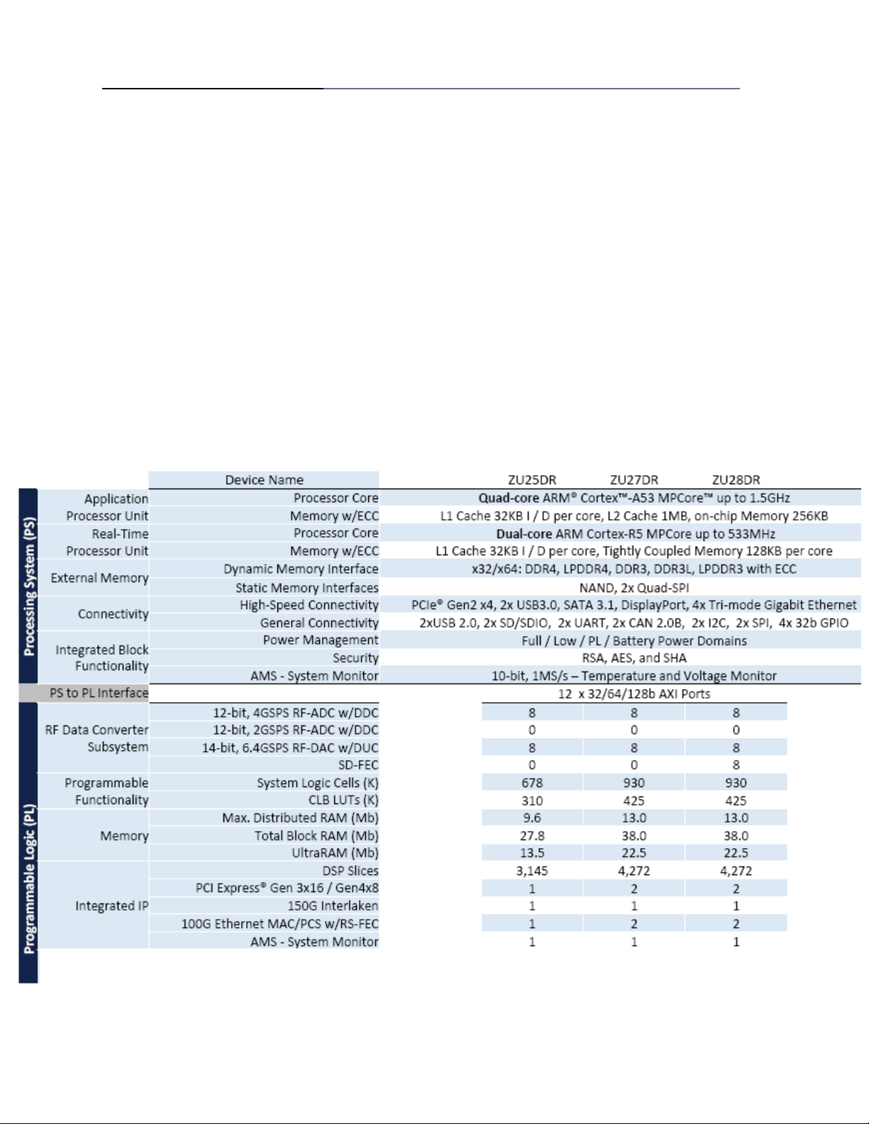
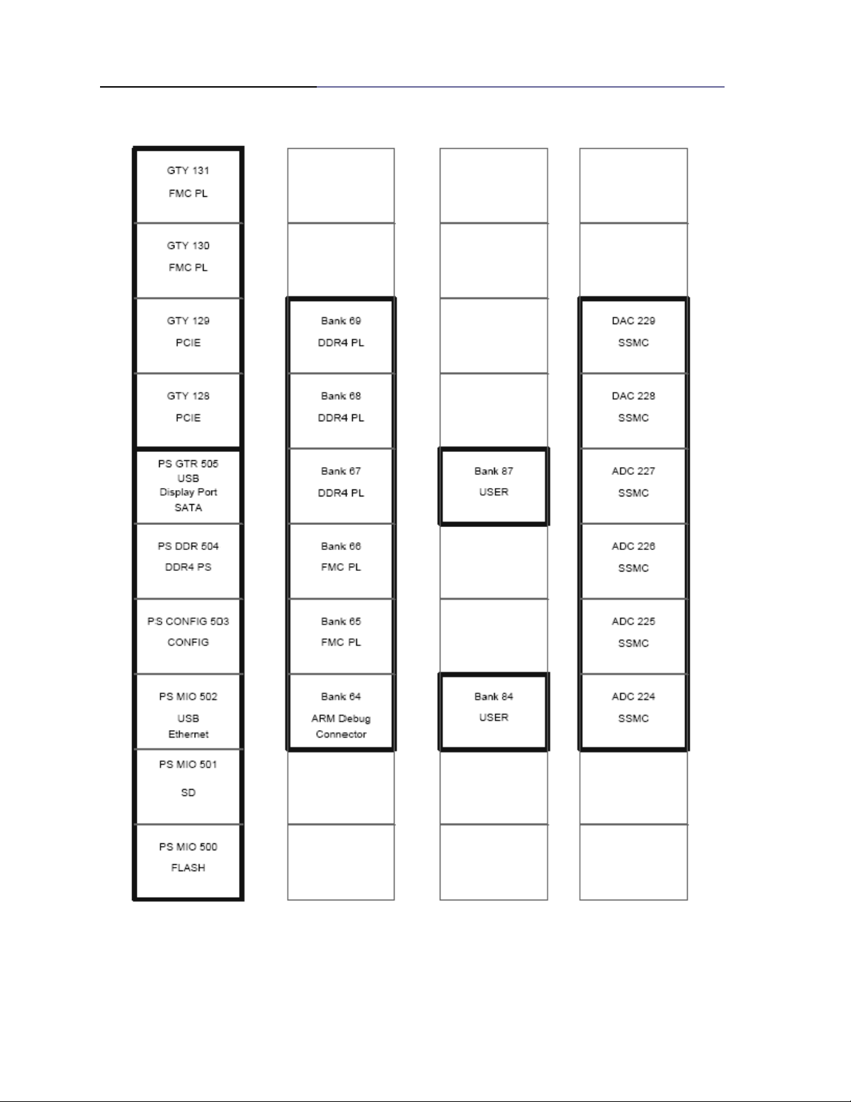
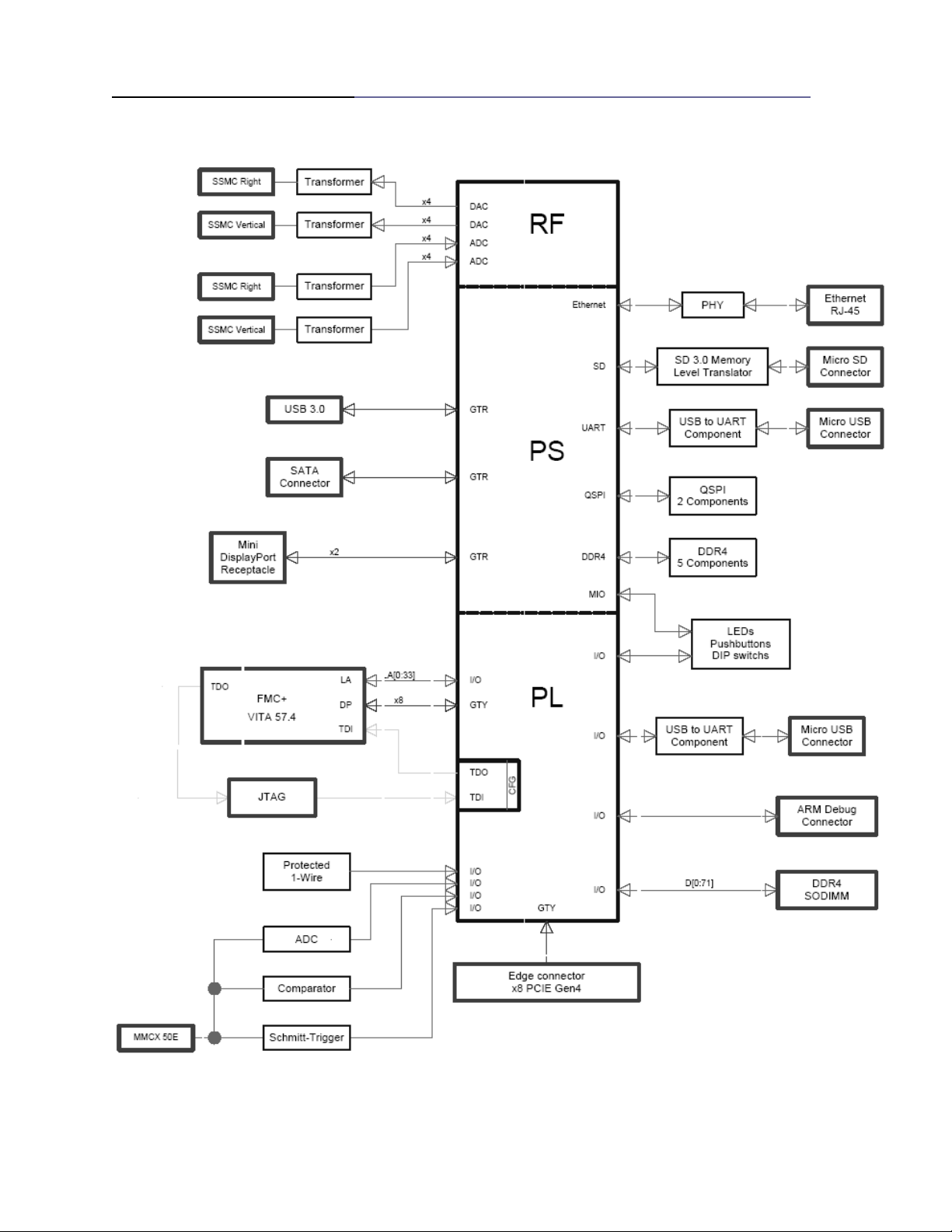
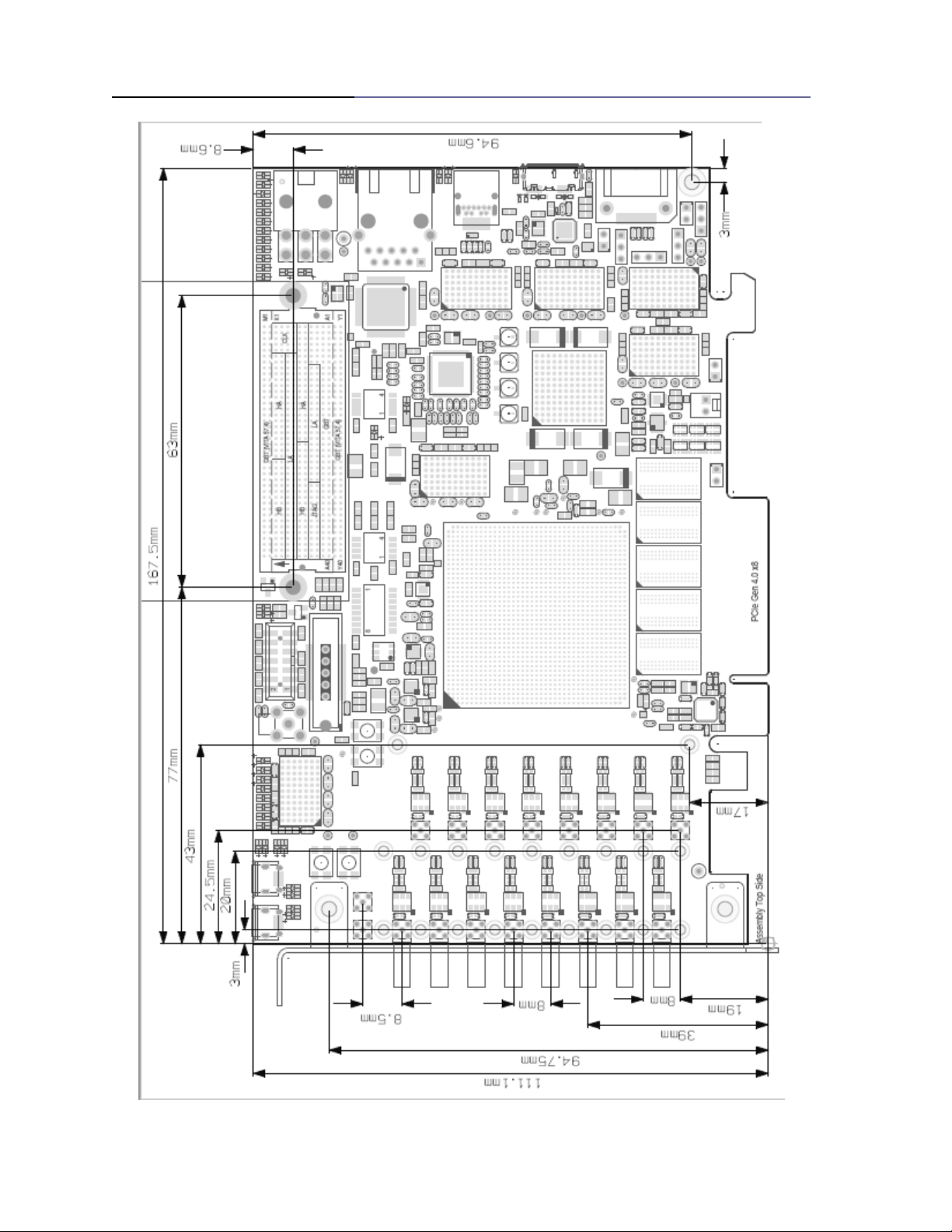
◙ 3.0) Banks Assignment, Block Diagram, Clocks Diagram & Mechanical Drawing
Figure (1) , (2), (3) and (4) illustrate FPGA I/O bank assignment, block diagram , clocks diagram, and
mechanical dimensions of the HTG-ZRF8 platform.
www.HiTechGlobal.com
7
HTG-ZRF8 Platform User Manual
Figure (1): FPGA Bank Assignment
www.HiTechGlobal.com
8
HTG-ZRF8 Platform User Manual
Figure (2): System Block Diagram
www.HiTechGlobal.com
9
HTG-ZRF8 Platform User Manual
Figure (3): Clock Block Diagram
www.HiTechGlobal.com
10
HTG-ZRF8 Platform User Manual
Figure (4): Mechanical Drawing
www.HiTechGlobal.com
11
Source
Part Number (Manufacturer)
Default Value
Clock Function
U19
Si5341A
Programmable
User, DDR 4 , FMC+, Processor GTR & SMP
U40
SIT8103AC-23-18E-33.33333MHz
33.33 MHz
Processor
U4
871S1022EKLF (IDT)
100 MHz
PCI Express
U68
LMX2592RHA
Programmable
ADC & DAC
U69
VCC6-LAB-122M880000
122.88 MHz
ADC & DAC Input
ZQ1
7M-25.000MEEQ-T (not installed)
25 MHz
PCIe Standalone
ZQ2
7M48072002
48 MHz
U19 Main Reference
ZQ3
FA-238 25.0000MB
25 MHz
Ethernet
ZQ4
FA-238 24.0000MB
24 MHz
USB2
ZQ5
9HT10-32.768KDZF-T
32.768 KHz
PS_PADI/PS_PADO RTC
X1/X2
Mini SMP
Variable
U19 Additional External Output
X3/X4
SSMC Connector
Variable
U19 Additional External Input
HTG-ZRF8 Platform User Manual
◙ 4.0) Clocks
The HTG-ZRF8 provides combination of fixed, programmable, and adjustable ultra-low-jitter clock sources for
different interfaces as summarized by the table (2).
Table (2): Main Clocks
►The ICS871S1022 (U4 )is a PLL-based clock generator specifically designed for PCI Express Clock
Generation applications. The device generates 100MHz, 125MHz, 250MHz or 500MHz from either a 25MHz
fundamental mode crystal or a 100MHz recovered clock. The ICS871S1022 has two modes of operation: (1)
high frequency jitter attenuator and (2) high performance clock synthesizer mode. When in jitter attenuator
mode, the ICS871S1022 is able to both suppress high frequency noise components and function as a frequency
translator. Designed to receive a jittery and noisy clock from an external source, the ICS871S1022 uses
FemtoClock® technology to clean up the incoming clock and translate the frequency to one of the four common
PCI Express frequencies. When in synthesizer mode, the device is able to generate high performance SSC and
non-SSC clocks from a low cost external, 25MHz, fundamental mode crystal. The ICS871S1022 uses
FemtoClock® technology to generate low noise clock outputs capable of providing the seed frequencies for the
common PCI Express link rates.
Additional product information is available at http://www.idt.com/products/clocks-timing/application-specificclocks/pci-express-pcie-clocks/871s1022-differential-07v-differential-pci-express-jitter-attenuator
►The any-frequency, any-output Si5341(U19) clock generator combines a wide-band PLL with proprietary
MultiSynth fractional synthesizer technology to offer a versatile and high performance clock generator
platform. This highly flexible architecture is capable of synthesizing a wide range of integer and no-integer
related frequencies up to 712.5 MHz on 10 differential clock outputs while delivering sub-100 fs rms phase
jitter performance with 0 ppm error. Each of the clock outputs can be assigned its own format and output
voltage enabling the Si5341/40 to replace multiple clock ICs and oscillators with a single device making it a
true “clock tree on a chip”.
The Si5341/40 can be quickly and easily configured using ClockBuilder Pro software. The device can be
programmed in circuit via I2C and SPI serial interfaces or using Silicon Labs’ dongle and the J28 header.
https://www.silabs.com/products/development-tools/software/clockbuilder-pro-software
www.HiTechGlobal.com

12
HTG-ZRF8 Platform User Manual
Figure (5): Si5341 Clock Generator Block Diagram
www.HiTechGlobal.com

13
Output #
Signal Name
Destination
FPGA Pin
Number
OUT0_P
CLK_PL_USER1_P
FPGA Bank 87
(User Clock)
C8
OUT0_N
CLK_PL_USER1_N
C7
OUT1_P
SYS_CLK_DDR4_PL_P
FPGA Bank67
(DDR4 SODIMM Clock)
G13
OUT1_N
SYS_CLK_DDR4_PL_N
G12
OUT2_P
FMC_PL_REFCLK_C2M_P
FMC + Connector
(Carrier to Mezzanine Clock)
-
OUT2_N
FMC_PL_REFCLK_C2M_N
-
OUT3_P
GTY_131_REFCLK_P
FPGA GTY 131
(FMC+ DP4-DP7)
P31
OUT3_N
GTY_131_REFCLK_N
P32
OUT4_P
GTY_130_REFCLK_P
FPGA GTY 130
(FMC+ DP0-DP3)
U33
OUT4_N
GTY_130_REFCLK_N
U34
OUT5_P
CLK_PL_USER2_P
FPGA Bank 64
(User Clock)
AM15
OUT5_N
CLK_PL_USER2_N
AN15
OUT6_P
GTR_505_REFCLK3_P
FPGA GTR 505
(USB3/SATA/Display Port)
AC34
OUT6_N
GTR_505_REFCLK3_N
AC35
OUT7_P
CLK_OUT_SMA_P
X1 /X2 Mini SMP Connector
(Output Clock)
-
OUT7_N
CLK_OUT_SMA_N
-
OUT8_P
GTR_505_REFCLK2_P
FPGA GTR 505
(USB3/SATA/Display Port)
AE34
OUT8_N
GTR_505_REFCLK2_N
AE35
OUT9_P
GTR_505_REFCLK1_P
FPGA GTR 505
(USB3/SATA/Display Port)
AG34
OUT9_N
GTR_505_REFCLK1_N
AG35
HTG-ZRF8 Platform User Manual
Table (3) provides summary of clock outputs of the Si5341 (U46) clock generator.
Table (3): Summary of the Si5341 (U46) Clock Outputs
►The LMX2592 (U68) is a high performance wideband synthesizer (PLL with integrated VCO). The output
frequency range is from 20 MHz to 5.5 GHz. The VCO core covers an octave from 3.55 to 7.1 GHz. The output
channel divider covers the frequency range from 20 MHz to the low bound of the VCO core.
The input signal frequency has a wide range from 5 to 1400 MHz. Following the input, there is an
programmable OSCin doubler, a pre-R divider (previous to multiplier), a multiplier, and then a post-R divider
(after multiplier) for flexible frequency planning between the input (OSCin) and the phase detector.
The phase detector (PFD) can take frequencies from 5 to 200 MHz, but also has extended modes down to 0.25
MHz and up to 400 MHz. The phase-lock loop (PLL) contains a Sigma-Delta modulator (1st to 4th order) for
fractional N-divider values. The fractional denominator is programmable to 32-bit long, allowing a very fine
resolution of frequency step. There is a phase adjust feature that allows shifting of the output phase in relation
to the input (OSCin) by a fraction of the size of the fractional denominator.
The output power is programmable and can be designed for high power at a specific frequency by the pullup
component at the output pin.
The digital logic is a standard 4-wire SPI or uWire interface and is 1.8-V and 3.3-V compatible.
www.HiTechGlobal.com
 Loading...