Hitachi Kokusai Electric UM04KO User Manual
Version 1.0
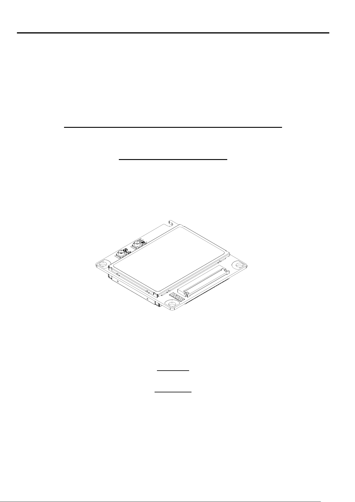
LTE Ubiquitous Module®(UM04-KO)
Instruction Manual
Version 1.0
August 2015

Version 1.0
― Contents ―
Introduction ...................................................................................................................................................................................................... 3
■Dimensional outline drawing ............................................................................................................................................................ 4
■Interface for the external device ...................................................................................................................................................... 5
■Available services with this device .................................................................................................................................................. 6
Device specification ...................................................................................................................................................................................... 7
Main specification.......................................................................................................................................................................................... 7
Interface ........................................................................................................................................................................................................ 9
1.Main connector ............................................................................................................................................................................... 9
2.Power supply ................................................................................................................................................................................. 19
3.UART interface ............................................................................................................................................................................ 28
4.USB interface ................................................................................................................................................................................ 33
5.Monitor interface ......................................................................................................................................................................... 35
6.UIM card interface ..................................................................................................................................................................... 38
7.RF connector (Main/Sub) ......................................................................................................................................................... 40
8.External antenna ......................................................................................................................................................................... 41
Precautions for connecting to the external device .......................................................................................................................... 42
Precaution for design of the external device .................................................................................................................................. 42
Recommended installation method ..................................................................................................................................................... 43
■In case of using the flexible connector ................................................................................................................................... 43
■In case of using the BtoB connector ........................................................................................................................................ 43
■Antenna connection ...................................................................................................................................................................... 44
Operation mode ............................................................................................................................................................................................ 45
Communication mode .............................................................................................................................................................................. 45
Service function ........................................................................................................................................................................................... 47
Packet communication ........................................................................................................................................................................... 47
SMS .............................................................................................................................................................................................................. 49
Area Mail ..................................................................................................................................................................................................... 49
Software update ....................................................................................................................................................................................... 50
RF part ON/ OFF function .................................................................................................................................................................... 50
AT command ................................................................................................................................................................................................. 51
AT command list....................................................................................................................................................................................... 51

Version 1.0
Introduction
Introduction
Please note that “UM04-KO” is referred to as “this device” in this instruction manual.
This device is the communication module which unified in combination with the radio part of the cellular telephone
and the modem part.
This device has the functions of packet communication and SMS.
As this device is built-in to the external device product, the LTE communication service (only in Japan) and
W-CDMA/GSM communication service (out of Japan) can be used.
This device is an environment-conscious product which is compliant with the RoHS Directive.
3
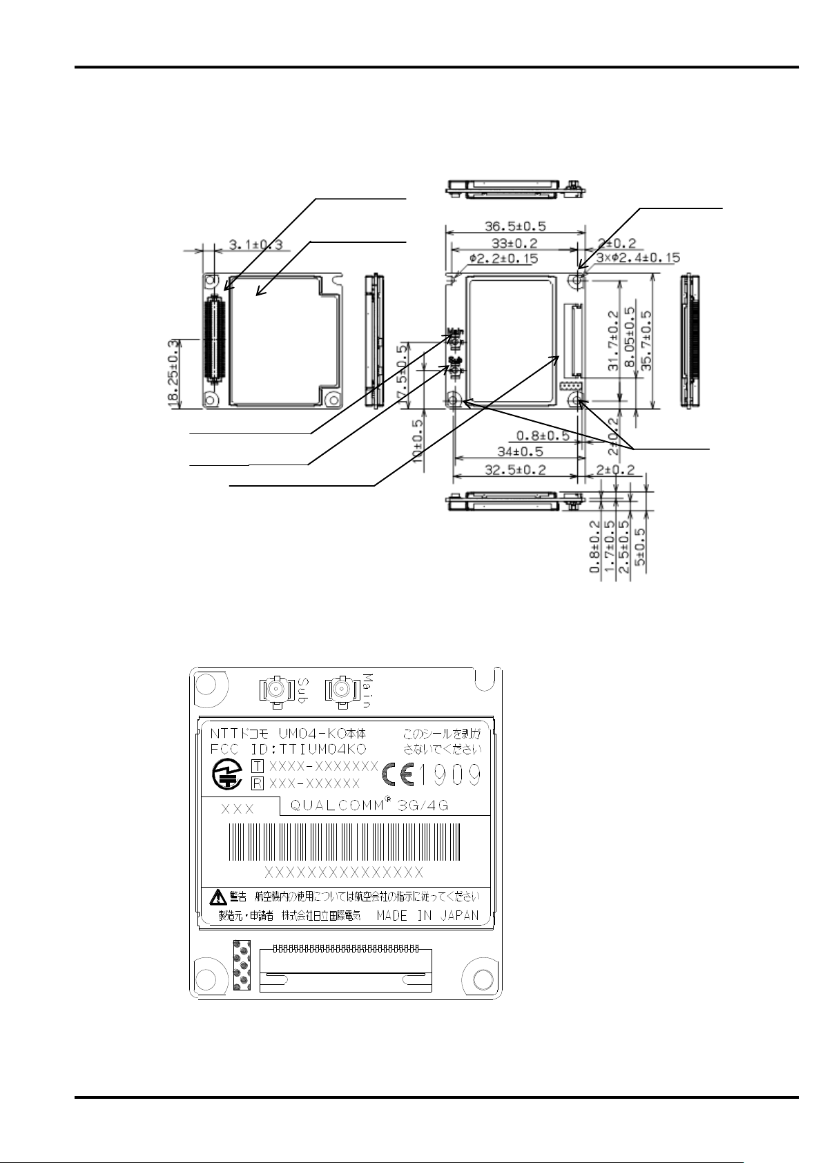
RF connector (MAIN)
Shield case
(Insulation label)
Mounting hole
Mounting hole
Main connector (BtoB)
Main connector (flexible)
RF connector (SUB)
Unit: mm
■Dimensional outline drawing
Version 1.0
●Name plate seal outline drawing
4
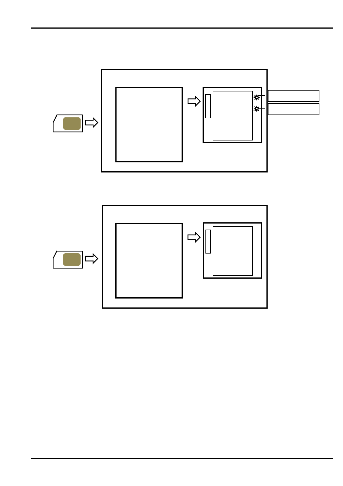
UIM card
Main connector
(flexible connector)
・Power supply
・Power supply Control
・UARTserial interface
・Monitor interface
・UIM card interface
External device
This device
(A-side)
RF connector (Sub)
RF connector (Main)
UIM card
Main connector
(BtoB connector)
・Power supply
・Power supply Control
・UARTserial interface
・USB interafce
・Monitor interface
・UIM card interface
External device
This device
(B-side)
■Interface for the external device
●Interface between this device and the external device (A-side : Flexible connector)
Version 1.0
●Interface between this device and the external device (B-side : BtoB connector)
This device has two main connectors. One is flexible connector on A-side and another is BtoB connector on
B-side. They each contain the interface of power supply, UART , USB (only in case of BtoB connector), UIM
card. RF connectors on A-side are used to connect the external antennas.
5

Version 1.0
■Available services with this device
This device can use various communication services of DOCOMO. Packet communication, SMS and other
associated various services are available.
In addition, for the use of the service, production of the external device which incorporated this device is necessary.
●Packet communication
Packet communication (packet switching) is communication method that transmits and receives divided data
which is partitioned into the unit of called packet (package).
Because the packet communication can use one line in common by plural external devices or applications, it can
communicate efficiently.
The data communication speed is 112.5Mbps for downlink and 37.5Mbps for uplink (best effort type) in LTE
network, and 42.2Mbps for downlink and 5.7Mbps for uplink (best effort type) in W-CDMA network.
●SMS
SMS (short message service) is the service that can transmit and receive the letter message of the short sentence
easily with the address which is same to phone number regardless of the mobile phone career through SMS center
of DOCOMO.
●Area Mail
Early warning “Area Mail” service is the service in Japan that earthquake early warning and tsunami warning
from Japan Meteorological Agency and the disaster and the refuge information from the country and the regional
public institution are delivered to cellphones and communication models which exist in the particular area all at
once through the DOCOMO network.
Please refer to the website of DOCOMO for the regional public institution which started service of the disaster
and the refuge information using Area Mail.
This device can not receive Area Mail at the place of weak radio wave.
During packet and other communication, it may receive Area Mail depending on communication situation. In
addition, it can not receive the Area Mail again that it missed to receive.
The reception of Area Mail is free of charge.
●Software update
This is the function to update the software of this device in LTE network after sale.
6
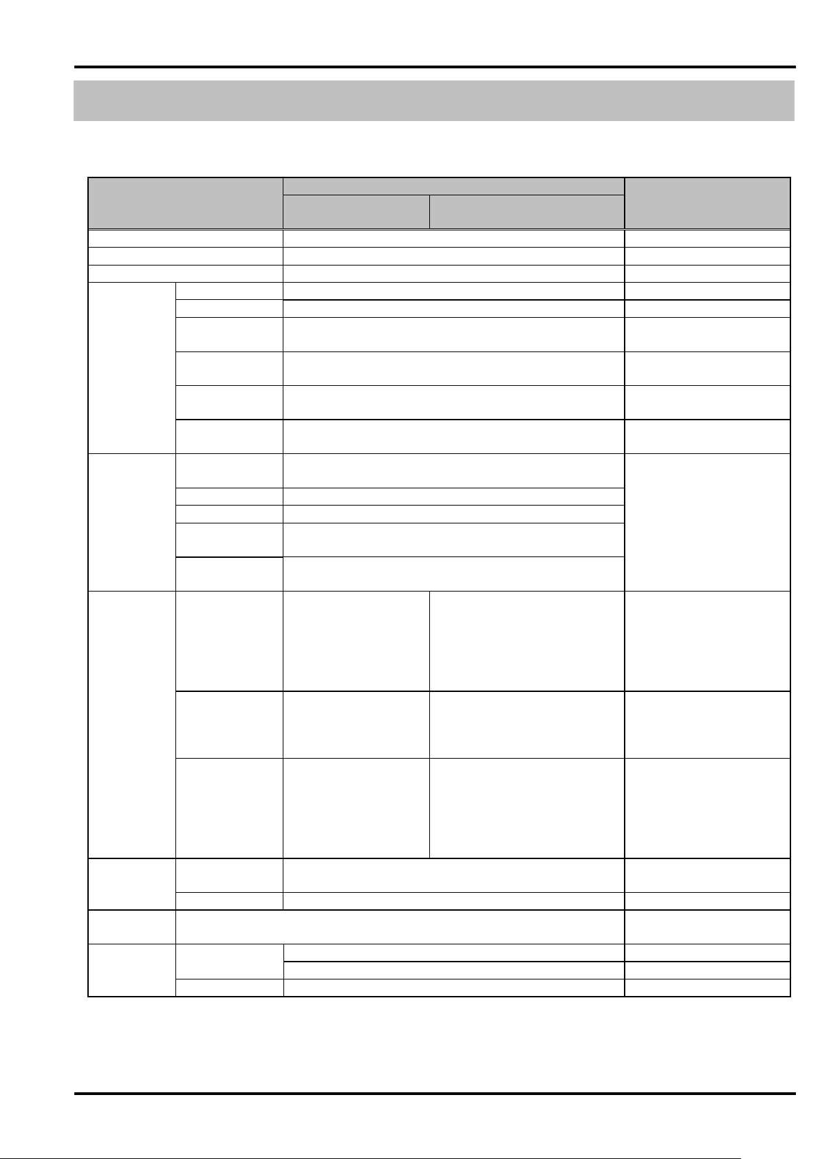
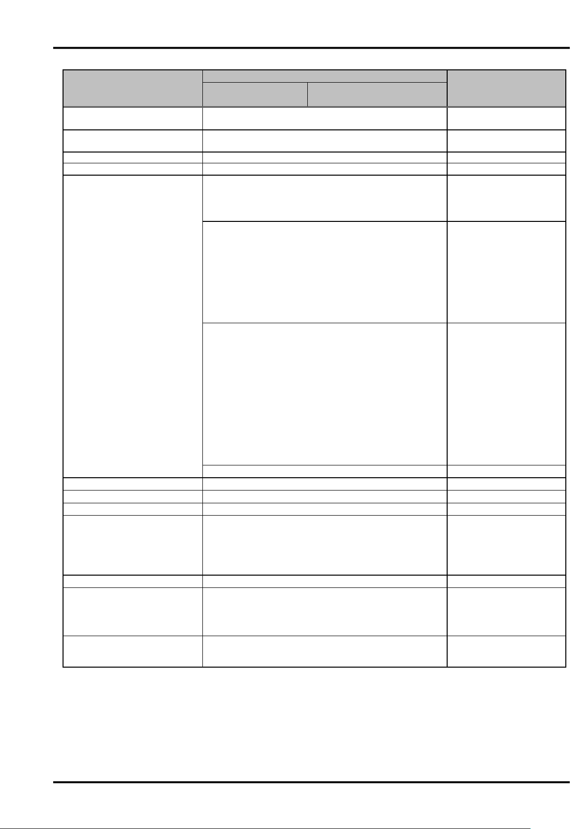
Device specification
Item
Description
Remarks
LTE mode
(LTE method)
Roaming mode
(W-CDMA/GSM method)
Supported service
Packet communication, SMS
-
Communication protocol
PPP, IP
-
Control method
AT command
-
UART serial
interface
Number of ports
One line
-
Signals
SD、RD、XER、XDR、XRS、XCS、XCD、XCI
-
Communication
speed (bps)
1200/2400/4800/9600/19200/38400/
57600/115200/230400/460800
-
Communication
format
Start:1bit, Stop:1bit, Data:8bit, Parity:none
-
Sending/Receivin
g control
Support hardware flow control, software flow control,
and without flow control
-
Baud rate
deviation
Sending:2% or less
Receiving:2% or less
-
USB interface
Communication
standard
Conformity USB2.0
Supported in case of BtoB
connector
Number of ports
One line
Function
Device function
Communication
speed
HS:480Mbps, FS:12Mbps
Signals
USB_DPLUS、USB_DMINUS、USB_VBUS、
USB_D_RDY_n、USB_H_RDY_n
RF interface
Radio frequency
2GHz/800MHz Band
【W-CDMA method】
2GHz/800MHz Band
【GSM method】
GSM850MHz/ GSM900MHz/
GSM1800MHz/
GSM1900MHz
-
Access method
OFDMA, SC-FDMA
【W-CDMA method】
DS-CDMA, T-HCDMA
【GSM method】
TDMA
-
Data
communication
speed
Uplink :37.5Mbps Max
Downlink :112.5Mbps
Max
【W-CDMA method】
Uplink : 5.7Mbps Max
Downlink: 42.2Mbps Max
【GSM method】
Uplink : 237kbps Max
Downlink: 237kbps Max
Best effort type
Monitor
interface
BtoB connector
ANT1_n, ANT2_n, TRX_n, LEDG_n, LEDGMS_n, ADL_n、
3G / LTE (GSM), SMS_n, CBS_ETWS_n
-
Flexible connector
PACKET, ANT1, ANT2, ANT3, LEDG, LEDR, LEDGMS
-
UIM card
interface
Conformity to 3GPP TS31series
External
interface
Main connector
80pin BtoB connector
-
57 pin flexible connector
-
Antenna connector
U.FL×2 (Main, Sub)
-
Device specification
Main specification
Version 1.0
7
Version 1.0
Item
Description
Remarks
LTE mode
(LTE method)
Roaming mode
(W-CDMA/GSM method)
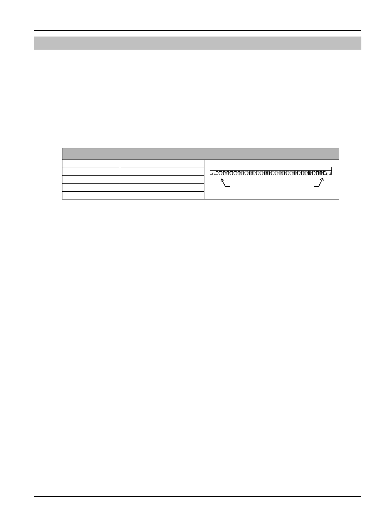
Operation environment
Temperature:-30℃ to +60℃
Humidity:25% to 85% (Without condensation)
-
Storage environment
Temperature:-40℃ to +85℃、
Humidity:25% to 85% (Without condensation)
Without electrical and
mechanical stress
Power supply voltage
DC+3.3V to 4.2V
Recommendation DC+3.7V
Power supply ripple
50mVp-p (0Hz to 2.5GHz) or less
-
Current consumption
During communication:TBD mA or less
Measurement condition: 500
ms average.
With output of maximum TX
power
Stand-by state:TBD mA or less
Stationary state in in-service
area
Without neighbor cell search.
ER-OFF
USB:inactive
DRX cycle:2.56 sec
Environment temperature:
25℃±2℃
Power supply voltage:3.7V
Inrush current drain:TBD A or less (Within 100μsec)
Power supply voltage
condition:
With the supply of the voltage
of 3.7V
(Which is voltage to reach to
the stable state in more than
300μs after start of power
supply).
Note) When supply the
voltage except the above
condition, inrush current drain
may exceed the value stated.
Peak current drain:TBD A or less
-
Dimensions
Approx. 36.5(W)×Approx. 35.7(D)×Approx. 5.0(H) mm
Without convex part
Weight
Approx. 11g
-
Electrostatic withstand voltage
±1kV (all pins)
-
Vibration condition
After a vibration of 19.6m/s2 (2G) acceleration and the frequency
of 30 to 100 Hz is applied to this device with the one cycle
sweeping time of 20 minutes for up/down, left/right, and
back/forth directions, the function and performance of this device
is normal with no damage or dropped parts observed.
-
Environmental compliance
RoHS compliant
-
Technical standard conformity proof
(the construction design
certification by the registration
proof institution)
Construction design certification number:TBD
-
Technical standard conformity
certification of the terminal
equipment
Certification number: TBD
-
8
Version 1.0
Connector specification
Number of pins
57
Pin pitch
0.3 ㎜
Connection type
Connector for FPC
Model number
57FXL-RSM1-S-H-G-TB(LF)(SN)
Manufacturer
JST CO., LTD
1
57
Interface
Interface
1.Main connector
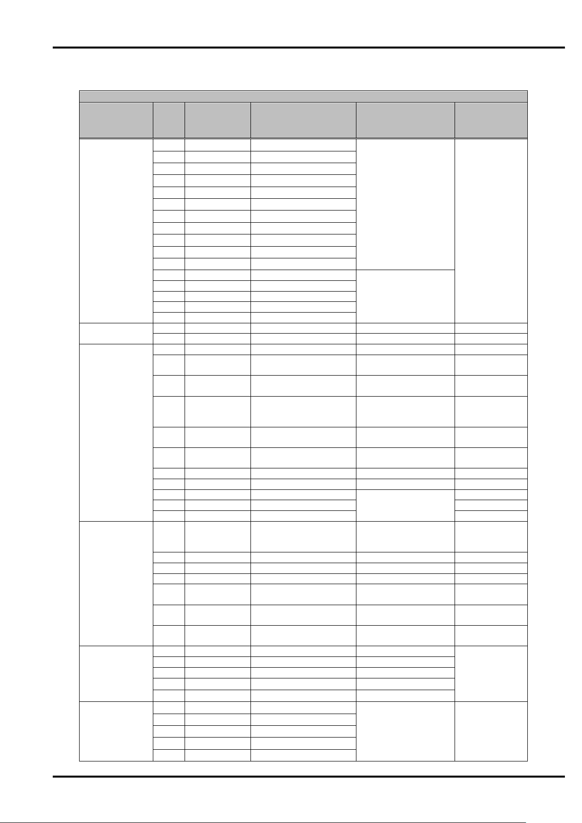
This device has two main connectors. One is flexible connector on the A-side and another is BtoB connector on
the B-side. They each contain the interface of power supply, UART , USB (only in case of BtoB connector), UIM
card. RF connectors on A-side are used to connect the external antennas.
■Flexible connector
This flexible connector is same as one used in UM01/02 series.
9
Connector Pin
Type
Pin
No.
Pin Name
Signal Direction
(UM04-KO ⇔
external device)
Signal Function
Setting of
unused pins
Power supply
1
SG
-
Grounding
Unconnection
prohibited
20
SG
-
22
SG - 23
SG - 28
SG - 33
SG
-
37
SG
-
51
SG
-
53
SG
-
55
SG
-
57
SG
-
2
VCC
←
Power Supply
(3.3 to 4.2V)
4
VCC
←
6
VCC
←
48
VCC
←
50
VCC
←
Power supply
control
30
PWRKEY
←
Power ON/OFF request
Open
43
SYSRST
←
System reset
Open
UARTserial
interface
41
XCD
→
Carrier detection signal
Open
39
XCI → Incoming call indication
signal
Open
35
XCS → Permission signal of
sending from this device
Open
32
XRS ← Request signal of
sending from external
device
Open
31
XER
←
Ready signal from
external device
Open
29
XDR
→
Ready signal from this
device
Open
27
RD → Received data
Open
25
SD ← Sending data
Open
19
DTE1
←
External device serial
communication data
speed configuration
Open
17
DTE2
←
Open
21
DTE3
←
Open
Monitor interface
13
PACKET
→
In packet service
area/Out of packet
service area
Open
11
ANT3
→
Antenna indication 3
Open
9
ANT2
→
Antenna indication 2
Open
7
ANT1
→
Antenna indication 1
Open
40
LEDG
→
For communication
status display
Open
36
LEDR
→
For communication
status display
Open
34
LEDGMS
→
For communication
status display
Open
UIM card
interface
18
SIM_VCC(C1)
→
Power to the UIM card
Unconnection
prohibited
15
SIM_RST(C2)
→
Reset signal
14
SIM_CLK(C3)
→
Clock signal
12
SIM_GND(C5)
-
Ground
10
SIM_DIO(C7)
⇔
Data input/output
Maintenance
interface
3
N.C.
-
Manufacturer
maintenance
Connection
prohibited
16
N.C.
-
26
N.C. - 38
N.C. - 42
N.C.
-
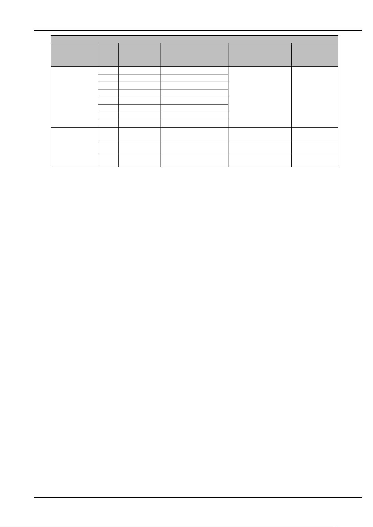
●Assignment of connector pins
Version 1.0
10
Version 1.0
Connector Pin
Type
Pin
No.
Pin Name
Signal Direction
(UM04-KO ⇔
external device)
Signal Function
Setting of
unused pins
44
N.C. - 45
N.C. - 46
N.C.
-
47
N.C.
-
49
N.C.
-
52
N.C.
-
54
N.C. - 56
N.C.
-
N.C.
5
N.C. - Not used
Connection
prohibited
8
N.C. - Not used
Connection
prohibited
24
N.C. - Not used
Connection
prohibited
11
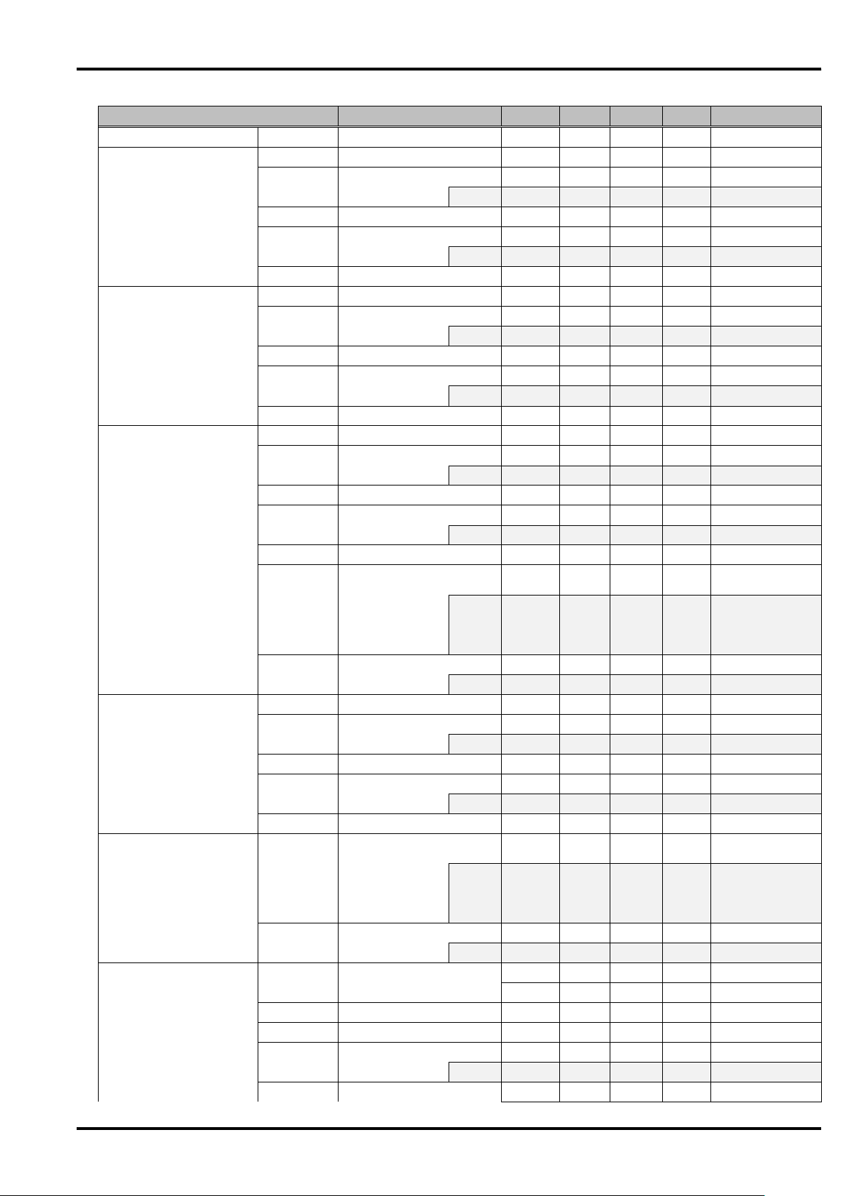
●Electrical characteristics
Item
Pin No.
Min
Typ
Max
Unit
Remarks
Power supply input
VCC
2,4,6,48,50
3.3
3.7
4.2
V
-
Power supply control
PWRKEY
VT+
30
0.77
-
1.44
V
Schmitt trigger
VIH
30
1.44
-
5.25
V -
ILEAK
-
-
10
μA
-
VT-
30
0.33
-
0.77
V
Schmitt trigger
VIL
30
0 - 0.33
V -
ILEAK
-
-
-10
μA
-
Hysteresis
30
0.34 - 0.8
V
-
Power supply control
SYSRST
VT+
43
0.7
1.1
1.5
V
Schmitt trigger
VIH
43
1.5 - 5.25
V
-
ILEAK
-
-
10
μA
-
VT-
43
0.25
0.61
0.9
V
Schmitt trigger
VIL
43
0 - 0.25
V
-
ILEAK
-
-
-10
μA
-
Hysteresis
43
0.15
0.49 1 V
-
UARTserial interface
XCD, XCI, XCS, XRS,
XER, XDR, SD, RD
VT+
25,31,32
0.7
1.1
1.5
V
Schmitt trigger
VIH
25,31,32
1.5 - 5.25
V
-
ILEAK
-
-
30
μA - VT-
25,31,32
0.25
0.61
0.9
V
Schmitt trigger
VIL
25,31,32
0 - 0.25
V
-
ILEAK
-
-
-2
mA
-
Hysteresis
25,31,32
0.15
0.49 1 V
-
VOH
27,29,35,39,41
-
-
5.25
V
Equivalent to open
circuit imp.
IOH
- - -
mA
There is no
definition because
of open drain
output
VOL
27,29,35,39,41
0 - 0.33
V
-
IOL - 2 - mA
-
Serial communication data
speed configuration
DTE1, DTE2, DTE3
VT+
17,19,21
0.7
1.1
1.5
V
Schmitt trigger
VIH
17,19,21
1.5 - 5.25
V
-
ILEAK
-
-
10
μA - VT-
17,19,21
0.25
0.61
0.9
V
Schmitt trigger
VIL
17,19,21
0 - 0.25
V
-
ILEAK
-
-
-10
μA - Hysteresis
17,19,21
0.15
0.49 1 V
-
Monitor interface
ANT1, ANT2, ANT3,
LEDR, LEDG,
LEDGMS, PACKET
VOH
7,9,11,13,34,36,40
-
-
5.25
V
Equivalent to
open circuit imp.
IOH
- - -
mA
There is no
definition because
of open drain
output
VOL
7,9,11,13,34,36,40
0 - 0.28
V -
IOL - 2 - mA
-
UIM card interface
SIM_VCC(C1)
SIM_RST(C2)
SIM_CLK(C3)
SIM_DIO(7)
Output
18
2.7 - 3.3
V
Class B
voltage
1.62
-
1.98
V
Class C
VIH
10
C1×0.7
-
C1+0.3
V
Class B/C
VIL
10
-0.3
-
C1×0.2
V
Class B/C
VOH
15
C1×0.8
-
C1
V
Class B/C
IOH - -1 - mA
Class B/C
VOL
15
0
-
C1×0.2
V
Class B/C
Version 1.0
12

Version 1.0
Item
Pin No.
Min
Typ
Max
Unit
Remarks
IOL
-
-
2
mA
Class B/C
VOH
10
C1×0.7
-
C1
V
Class B/C
IOH - -1 - mA
Class B/C
VOL
10
0 - 0.4
V
Class B
0 - 0.3
V
Class C
IOL
-
-
1
mA
Class B/C
VOH
14
C1×0.7
-
C1
V
Class B/C
IOH - -1 - mA
Class B/C
VOL
14
0
-
C1×0.2
V
Class B/C
IOL
-
-
2
mA
Class B/C
13
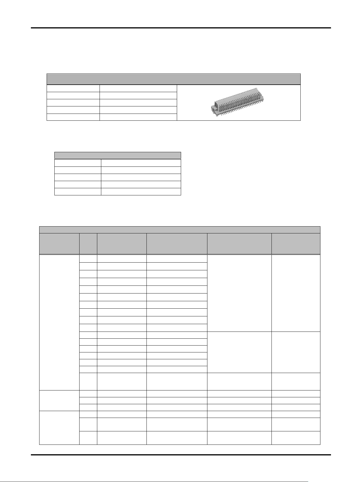
Connector specification
Number of pins
80 Pin pitch
0.5 ㎜
Connection type
Board to Board Connector
Model number
DF12(3.0)-80DS-0.5V(86)
Manufacturer
Hirose Electric CO., LTD.
Connector specification
Number of pins
80
Pin pitch
0.5mm
Connection type
Board to Board Connector
Model number
DF12B(3.0)-80DP-0.5V(86)
Manufacturer
Hirose Electric CO., LTD.
Connector Pin
Type
Pin
No.
Pin Name
Signal Direction
(UM04-KO⇔external
device)
Signal Function
Setting of
Unused pins
Power supply
14
SG
-
Grounding
Unconnection
prohibited
18
SG - 21
SG - 31
SG - 34
SG - 37
SG - 38
SG - 39
SG
-
40
SG
-
51
SG
-
41
VCC
←
Power supply
(3.3 to 4.2V)
Unconnection
prohibited
42
VCC
←
43
VCC ← 44
VCC ← 45
VCC ← 46
VCC
←
49
BtoB_DET(SG)
-
BtoB connection
detection signal
Unconnection
prohibited
[Note1]
Power supply
control
5
PWRKEY_ON_n
←
Power ON request
Open
6
PWRKEY_OFF_n
←
Power OFF request
Open
4
SYSRST_n
←
System reset
Open
UARTserial
interface
76
XCD
→
Carrier detection signal
Open
80
XCI → Incoming call indication
signal
Open
78
XCS
→
Permission signal of
sending from this device
Open
■BtoB Connector
This flexible connector is same as one used in UM03-KO.
◆Please use the connector shown in the following table for the external device which connected to this device.
Version 1.0
●Assignment of connector pins
14
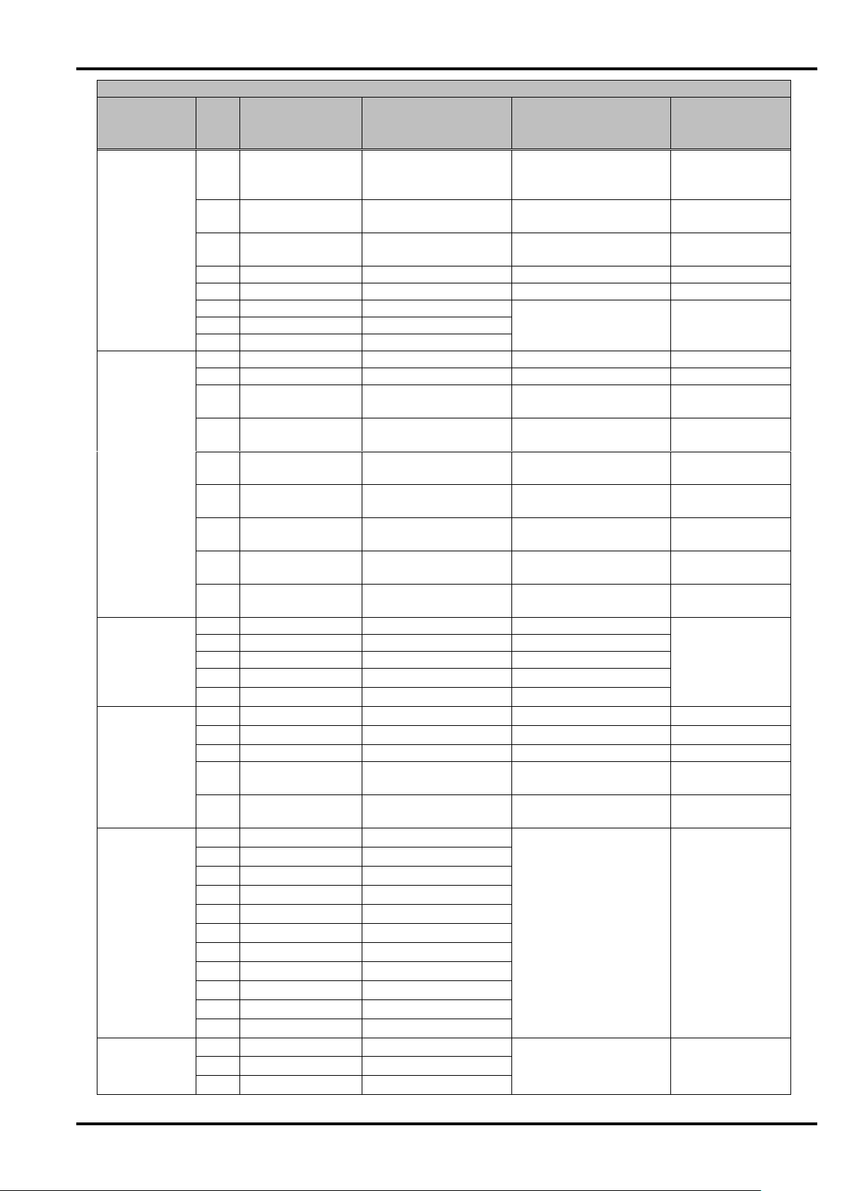
Version 1.0
Connector Pin
Type
Pin
No.
Pin Name
Signal Direction
(UM04-KO⇔external
device)
Signal Function
Setting of
Unused pins
1
XRS
←
Request signal of
sending from external
device
Open [Note2]
3
XER
←
Ready signal from
external device
Open [Note2]
79
XDR
→
Ready signal from this
device
Open
77
RD → Received data
Open
2
SD ← Sending data
Open [Note2]
10
DTE1
←
External device serial
communication data
speed configuration
Depends on
configured value
11
DTE2
←
12
DTE3
←
モニタ
インタフェース
71
ANT1_n
→
Antenna indication 1
Open
72
ANT2_n
→
Antenna indication 2
Open
70
TRX_n
→
Packet communication
status indication
Open
48
LEDG_n
→
Operation status
indication
Open
47
LEDGMS_n
→
Communication status
indication
Open
30
ADL_n
→
Software update status
indication
Open
68
SMS_n
→
Notification of SMS
receiving
Open
67
CBS_ETWS_n
→
Notification of Area
Mail receiving
Open
74
3G/LTE (GSM)
→
Attached network
indication
Open
UIM card
interface
54
SIM_VCC(C1)
→
Power supply
Unconnection
prohibited
52
SIM_RST(C2)
→
Reset Signal
55
SIM_CLK(C3)
→
Clock signal
56
SIM_GND(C5)
-
Grounding
53
SIM_DIO(C7)
⇔
Data input/output
USB interface
20
USB_DPLUS
⇔
Data signal +
Open
19
USB_DMINUS
⇔
Data signal -
Open
23
USB_VBUS
←
USB detection signal
Open
22
USB_H_RDY_n
←
Request of activation
from external device
Pull-down
[Note3]
66
USB_D_RDY_n
→
Request of activation
from this device
Open
Maintenance
interface
17
N.C.
-
Manufacturer
maintenance
Connection
prohibited
25
N.C.
-
58
N.C.
-
59
N.C.
-
60
N.C.
-
61
N.C.
-
62
N.C.
-
63
N.C.
-
64
N.C.
-
65
N.C.
-
73
N.C.
-
N.C.
7
N.C.
-
Not used
Connection
prohibited
8
N.C.
-
9
N.C.
-
15
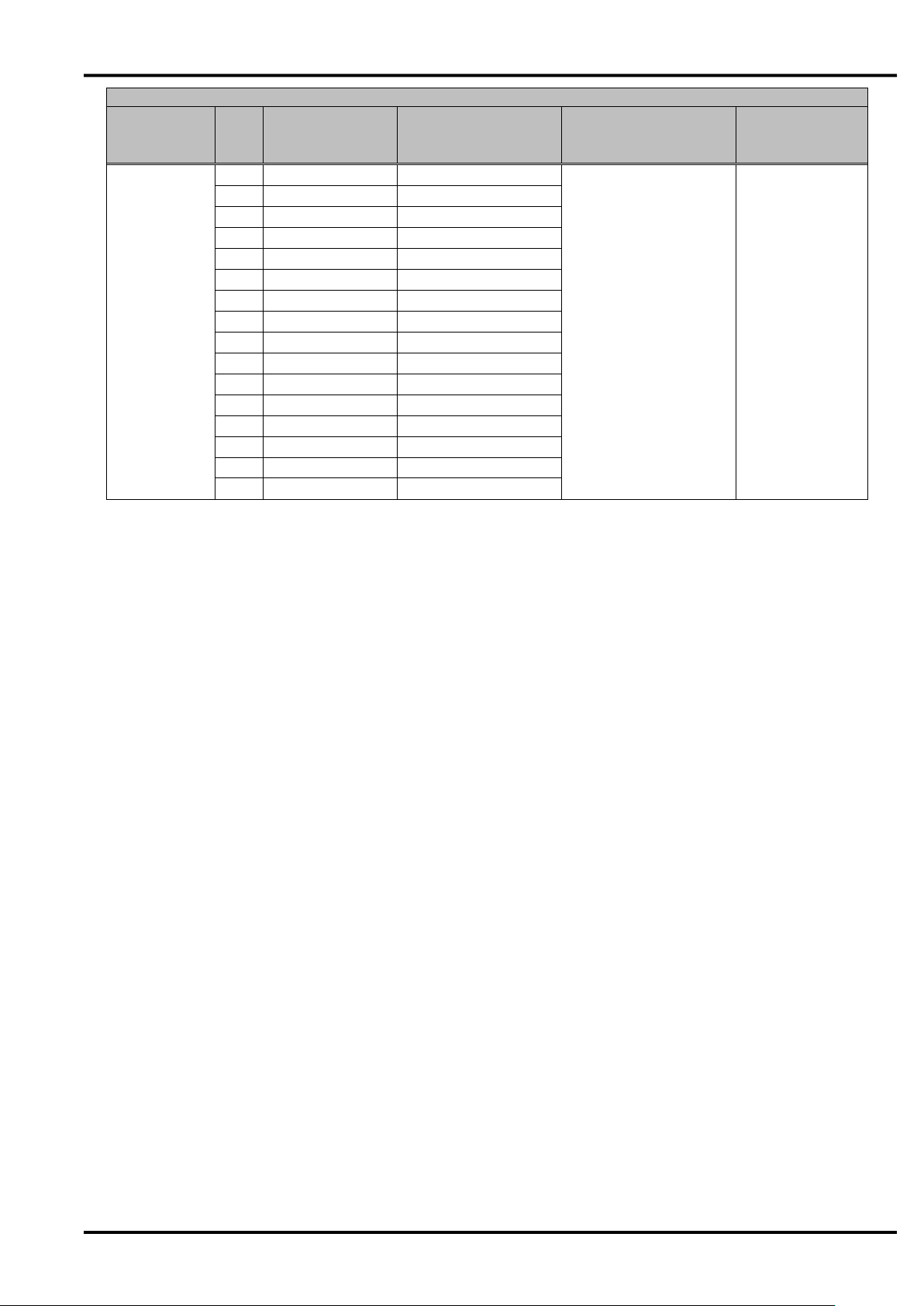
Version 1.0
Connector Pin
Type
Pin
No.
Pin Name
Signal Direction
(UM04-KO⇔external
device)
Signal Function
Setting of
Unused pins
13
N.C.
-
15
N.C.
-
16
N.C.
-
24
N.C.
-
26
N.C.
-
27
N.C.
-
28
N.C.
-
29
N.C.
-
32
N.C.
-
33
N.C.
-
35
N.C.
-
36
N.C.
-
50
N.C.
-
57
N.C.
-
69
N.C.
-
75
N.C.
-
[Note1] This signal is for the detection of BtoB connector connection. Please connect to SG without fail.
[Note2] The connection of the pull-up resistor is no problem. In case of connecting the pull-up resistor, please use the
power supply for pulling up within +1.8V to +5.25V.
[Note3] Recommended resistor value of the pulling down is 10kΩ to 100kΩ. Direct connection with SG is no problem.
16
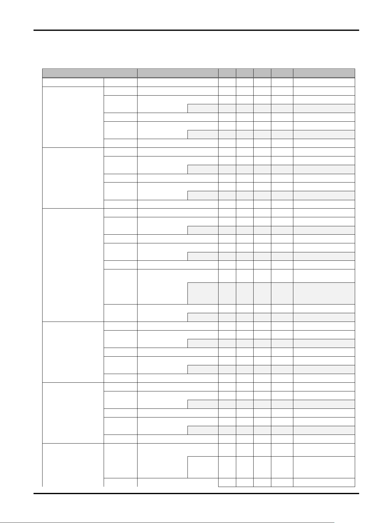
●Electrical characteristics
Item
Pin No.
Min
Typ
Max
Unit
Remarks
Power supply input
VCC
41,42,43,44,45,46
3.3
3.7
4.2
V
-
Power supply control
PWRKEY_ON_n
VT+ 5
0.77 - 1.44
V
Schmitt trigger
VIH 5
1.44 - 5.25
V -
ILEAK
-
-
10
μA
-
VT- 5
0.33 - 0.77
V
Schmitt trigger
VIL 5
0 - 0.33
V -
ILEAK
-
-
-10
μA
-
Hysteresis
5
0.34 - 0.8
V
-
Power supply control
PWRKEY_OFF_n
SYSRST_n
VT+
4,6
0.7
1.1
1.5
V
Schmitt trigger
VIH
4,6
1.5 - 5.25
V
-
ILEAK
-
-
10
μA
-
VT-
4,6
0.25
0.61
0.9
V
Schmitt trigger
VIL
4,6
0 - 0.25
V
-
ILEAK
-
-
-10
μA
-
Hysteresis
4,6
0.15
0.49 1 V
-
UARTserial interface
XCD, XCI, XCS, XRS,
XER, XDR, SD, RD
VT+
1,2,3
0.7
1.1
1.5
V
Schmitt trigger
VIH
1,2,3
1.5 - 5.25
V
-
ILEAK
-
-
30
μA
-
VT-
1,2,3
0.25
0.61
0.9
V
Schmitt trigger
VIL
1,2,3
0 - 0.25
V
-
ILEAK
-
-
-2
mA
-
Hysteresis
1,2,3
0.15
0.49 1 V
-
VOH
76,77,78,79,80
-
-
5.25
V
Equivalent to open
circuit imp.
IOH
- - -
mA
There is no definition
because of open drain
output
VOL
76,77,78,79,80
0 - 0.33
V
-
IOL - 2 - mA
-
Serial communication
data speed configuration
DTE1, DTE2, DTE3
VT+
10,11,12
0.7
1.1
1.5
V
Schmitt trigger
VIH
10,11,12
1.5 - 5.25
V
-
ILEAK
-
-
10
μA
-
VT-
10,11,12
0.25
0.61
0.9
V
Schmitt trigger
VIL
10,11,12
0 - 0.25
V
-
ILEAK
-
-
-10
μA
-
Hysteresis
10,11,12
0.15
0.49 1 V
-
USB interface
USB_H_RDY_n
VT+
22
0.7
1.1
1.5
V
Schmitt trigger
VIH
22
1.5 - 5.25
V
-
ILEAK
-
-
10
μA
-
VT-
22
0.25
0.61
0.9
V
Schmitt trigger
VIL
22
0 - 0.25
V
-
ILEAK
-
-
-10
μA
-
Hysteresis
22
0.15
0.49 1 V
-
USB_D_RDY_n
VOH
66
-
-
5.25
V
Equivalent to open
circuit imp.
IOH
- - -
mA
There is no definition
because of open drain
output
VOL
66
0 - 0.33
V
-
Current I regards its direction to flow into this device as plus.
Version 1.0
17
 Loading...