

TK No. 5204E
VT-FX240EUK
SERVICE MANUAL
VT-MX210EUK
This video deck is VHS type video
recorder. For proper operation, only
the VHS type cassette must be
used.
SPECIFICATIONS AND PARTS ARE SUBJECT TO CHANGE FOR IMPROVEMENT
VIDEO CASSETTE RECORDER
June 2002
Digital Media Division, Tokai

CONTENTS
CHAPTER 1 GENERAL INFORMATION
SPECIFICATIONS. . . . . . . . . . . . . . . . . . . . . . . . . . . . . 1-1-1
FUNCTION INDICATOR SYMBOLS . . . . . . . . . . . . . . 1-2-1
IMPORTANT SAFETY PRECAUTIONS . . . . . . . . . . . . 1-3-1
Product Safety Notice . . . . . . . . . . . . . . . . . . . . . . . . . 1-3-1
Precautions during Servicing. . . . . . . . . . . . . . . . . . . . 1-3-1
Safety Check after Servicing . . . . . . . . . . . . . . . . . . . . 1-3-2
STANDARD NOTES FOR SERVICING . . . . . . . . . . . . 1-4-1
Circuit Board Indications . . . . . . . . . . . . . . . . . . . . . . . 1-4-1
Instructions for Connectors . . . . . . . . . . . . . . . . . . . . . 1-4-1
How to Remove/Install Flat Pack-IC . . . . . . . . . . . . . . 1-4-1
Instructions for Handling
Semi-conductors . . . . . . . . . . . . . . . . . . . . . . . . . . . 1-4-3
PREPARATION FOR SERVICING . . . . . . . . . . . . . . . . 1-5-1
How to Enter the Service Mode. . . . . . . . . . . . . . . . . . 1-5-1
TROUBLESHOOTING . . . . . . . . . . . . . . . . . . . . . . . . . 1-6-1
ORERATING CONTROLS AND FUNCTIONS . . . . . . . 1-7-1
CHAPTER 2 DISASSEMBLY AND ADJUSTMENT
CABINET DISASSEMBLY INSTRUCTIONS . . . . . . . . 2-1-1
1. Disassembly Flowchart . . . . . . . . . . . . . . . . . . . . . . 2-1-1
2. Disassembly Method . . . . . . . . . . . . . . . . . . . . . . . . 2-1-1
DISASSEMBLY/ASSEMBLY PROCEDURES OF
DECK MECHANISM . . . . . . . . . . . . . . . . . . . . . . . . . . 2-2-1
ALIGNMENT PROCEDURES OF MECHANISM . . . . . 2-3-1
ELECTRICAL ADJUSTMENT INSTRUCTIONS . . . . . 2-4-1
Test Equipment Required . . . . . . . . . . . . . . . . . . . . . . 2-4-1
Head Switching Position Adjustment. . . . . . . . . . . . . . 2-4-1
FIXTURE AND TAPE FOR ADJUSTMENT . . . . . . . . . 2-5-1
How to Use The Fixtures. . . . . . . . . . . . . . . . . . . . . . . 2-5-1
MECHANICAL ALIGNMENT PROCEDURES . . . . . . . 2-6-1
Service Information . . . . . . . . . . . . . . . . . . . . . . . . . . . 2-6-1
1.Tape Interchangeability Alignment. . . . . . . . . . . . . . 2-6-2
1-A.Preliminary/Final Checking and
Alignment of Tape Path . . . . . . . . . . . . . . . . . . . 2-6-3
1-B.X Value Alignment . . . . . . . . . . . . . . . . . . . . . . . . 2-6-3
1-C.Checking/Adjustment of Envelope Waveform . . . 2-6-4
1-D.Azimuth Alignment of
Audio/Control/Erase Head . . . . . . . . . . . . . . . . .2-6-4
STANDARD MAINTENANCE . . . . . . . . . . . . . . . . . . . . 2-7-1
Service Schedule Components . . . . . . . . . . . . . . . . . . 2-7-1
Cleaning . . . . . . . . . . . . . . . . . . . . . . . . . . . . . . . . . . . 2-7-2
CHAPTER 4
SCHEMATIC DIAGRAMS/CBA’S AND
TEST POINTS. . . . . . . . . . . . . . . . . . . . . . . . . . . . . . . 4-1-1
Wiring Diagrams . . . . . . . . . . . . . . . . . . . . . . . . . . . . . 4-1-3
Main 1/5 Schematic Diagram . . . . . . . . . . . . . . . . . . . 4-1-4
Main 2/5 Schematic Diagram . . . . . . . . . . . . . . . . . . . 4-1-5
Main 3/5 Schematic Diagram . . . . . . . . . . . . . . . . . . . 4-1-6
Main 4/5 Schematic Diagram . . . . . . . . . . . . . . . . . . . 4-1-7
Main 5/5 Schematic Diagram ( VT-FX240EUK ). . . . . 4-1-8
Function Schematic Diagram . . . . . . . . . . . . . . . . . . . 4-1-9
AFV Schematic Diagram ( VT-FX240EUK ) . . . . . . . 4-1-10
Jack Schematic Diagram. . . . . . . . . . . . . . . . . . . . . . 4-1-11
Main CBA Top View . . . . . . . . . . . . . . . . . . . . . . . . . 4-1-12
Main CBA Bottom View. . . . . . . . . . . . . . . . . . . . . . . 4-1-13
Function/Power SW CBA Top/Bottom View . . . . . . . 4-1-14
AFV CBA Top/Bottom View. . . . . . . . . . . . . . . . . . . . 4-1-15
Jack CBA Top/Bottom View . . . . . . . . . . . . . . . . . . . 4-1-16
BLOCK DIAGRAMS . . . . . . . . . . . . . . . . . . . . . . . . . . . 4-2-1
Servo/System Control Block Diagram . . . . . . . . . . . . 4-2-1
Video Block Diagram(VT-MX210EUK) . . . . . . . . . . . . 4-2-2
Video Block Diagram(VT-FX240EUK). . . . . . . . . . . . . 4-2-3
Audio Block Diagram(VT-MX210EUK) . . . . . . . . . . . . 4-2-4
Audio Block Diagram(VT-FX240EUK). . . . . . . . . . . . . 4-2-5
Hi-Fi Audio Block Diagram(VT-FX240EUK) . . . . . . . . 4-2-6
Power Supply Block Diagram . . . . . . . . . . . . . . . . . . . 4-2-7
SYSTEM CONTROL TIMING CHARTS . . . . . . . . . . . . 4-3-1
IC PIN FUNCTION DESCRIPTIONS . . . . . . . . . . . . . . 4-4-1
LEAD IDENTIFICATIONS. . . . . . . . . . . . . . . . . . . . . . . 4-5-1
SCHEMATIC AND BLOCK DIAGRAMS/
CBA’S
CHAPTER 3 EXPLODED VIEWS AND PARTS LIST
EXPLODED VIEWS . . . . . . . . . . . . . . . . . . . . . . . . . . . 3-1-1
Front Panel . . . . . . . . . . . . . . . . . . . . . . . . . . . . . . . . . 3-1-1
Cabinet . . . . . . . . . . . . . . . . . . . . . . . . . . . . . . . . . . . . 3-1-2
Deck Mechanism View 1 . . . . . . . . . . . . . . . . . . . . . . . 3-1-3
Deck Mechanism View 2 . . . . . . . . . . . . . . . . . . . . . . . 3-1-4
Deck Mechanism View 3 . . . . . . . . . . . . . . . . . . . . . . . 3-1-5
REPLACEMENT PARTS LIST . . . . . . . . . . . . . . . . . . . 3-2-1
Mechanical Parts List . . . . . . . . . . . . . . . . . . . . . . . . . 3-2-1
Electrical Parts List . . . . . . . . . . . . . . . . . . . . . . . . . . . 3-2-3

CHAPTER 1 GENERAL INFORMATION
SPECIFICATIONS
VT-FX240EUK VT-MX210EUK
General Specifications
Television system: PAL I
Video heads Six comprising of Four-video
Tape width : 12.65mm
Tape speed
SP : 23.39mm/s
LP : 11.70mm/s
Tuner channel
RF converter : Built-in UHF converter
Converter output : UHF Channel 22 to 69
Timer indication : 24-hour system
Operating temperature : 5
Terminals
AERIAL : Coaxial type, male
RF OUT : Coaxial type, female
AUDIO/VIDEO : 21 pin scart socket x 2
AUDIO output
: RCA connector x 2
TV standard
and Two-audio heads
Helical scan system
IRA to IRJ
E21 to E69
CATV
(adjustable)
C to 40 C
Electrical Specifications
Video output level : 1Vp-p
Video output impedance : 75Ω unbalanced
Audio output level : -6dBv
Video input level : 0.5 to 2.0Vp-p
Audio input level : -10dBv
Video S/N ratio
(STANDARD): 45dB
Audio S/N ratio
(STANDARD): 41dB
General Specifications
Television system: PAL I
Video heads Rotary two-head
Tape width : 12.65mm
Tape speed
SP : 23.39mm/s
LP : 11.70mm/s
Tuner channel
RF converter : Built-in UHF converter
Converter output : UHF Channel 22 to 69
Timer indication : 24-hour system
Operating temperature : 5
Terminals
AERIAL : Coaxial type, male
RF OUT : Coaxial type, female
AUDIO/VIDEO :
TV standard
Helical scan system
IRA to IRJ
E21 to E69
CATV
(adjustable)
C to 40 C
21 pin scart socket x 2
Electrical Specifications
Video output level : 1Vp-p
Video output impedance : 75Ω unbalanced
Audio output level : -6dBv
Video input level : 0.5 to 2.0Vp-p
Audio input level : -10dBv
Video S/N ratio
(STANDARD): 45dB
Audio S/N ratio
(STANDARD): 41dB
Other Specifications
Power requirement : 220-240V to 50Hz
Power consumption : 20 Watts (Stand by:3.3 watts)
Dimensions : W 360mm
H 92mm
D 226mm
Weight : 2.6 kg. (approx.)
Designs and specifications are subject to change without notice.
Other Specifications
Power requirement : 220-240V to 50Hz
Power consumption : 20 Watts (Stand by: 3.3 watts)
Dimensions : W 360mm
H 92mm
D 226mm
Weight : 2.6 kg. (approx.)
1-1-1

FUNCTION INDICATOR SYMBOLS
Note:
The following symbols will appear on the indicator panel to indicate the current mode or operation of the VCR.
On-screen modes will also be momentarily displayed on the tv screen when you press the operation buttons.
Display panel
PWR. REC
" H "= LED Light on, " L "= LED Light off
LED MODE INDICATOR ACTIVE
CASSETTE "IN"
CASSETTE "OUT"
CLOCK " 88:88 "
POWER ON " PWR. " ON
REC " REC " ON
REC PAUSE " REC " Blinks at 0.8Hz interval
T-REC, OTR " " ON
When reel and capstan mechanism is not
functioning correctly
When tape loading mechanism is not functioning correctly
When cassette loading mechanism is not
functioning correctly
When the drum is not working properly " "
S-INH condition All modes Blinks at 0.8Hz interval
" "
" "
" PM "
" "
" 1 "
" "
" 2 "
" "
" 3 "
" 4 "
ON
OFF
ON
ON/OFF
(T-REC OFF, T-REC incomplete
Blinks at 0.8Hz interval)
Blinks at 0.8Hz interval
Blinks at 0.8Hz interval
Blinks at 0.8Hz interval
Blinks at 0.8Hz interval
1-2-1

IMPORTANT SAFETY PRECAUTIONS
Product Safety Notice
Some electrical and mechanical parts have special
safety-related characteristics which are often not evident from visual inspection, nor can the protection
they give necessarily be obtained by replacing them
with components rated for higher voltage, wattage,
etc. Parts that have special safety characteristics are
identified by a ! on schematics and in parts lists. Use
of a substitute replacement that does not have the
same safety characteristics as the recommended
replacement part might create shock, fire, and/or other
hazards. The Product’s Safety is under review continuously and new instructions are issued whenever
appropriate. Prior to shipment from the factory, our
products are carefully inspected to confirm with the
recognized product safety and electrical codes of the
countries in which they are to be sold. However, in
order to maintain such compliance, it is equally important to implement the following precautions when a set
is being serviced.
Precautions during Servicing
A. Parts identified by the ! symbol are critical for
safety. Replace only with part number specified.
B. In addition to safety, other parts and assemblies
are specified for conformance with regulations
applying to spurious radiation. These must also be
replaced only with specified replacements.
Examples: RF converters, RF cables, noise blocking capacitors, and noise blocking filters, etc.
C. Use specified internal wiring. Note especially:
1)Wires covered with PVC tubing
2)Double insulated wires
3)High voltage leads
D. Use specified insulating materials for hazardous
live parts. Note especially:
1)Insulation tape
2)PVC tubing
3)Spacers
4)Insulators for transistors
E. When replacing AC primary side components
(transformers, power cord, etc.), wrap ends of
wires securely about the terminals before soldering.
F. Observe that the wires do not contact heat produc-
ing parts (heatsinks, oxide metal film resistors, fusible resistors, etc.).
G. Check that replaced wires do not contact sharp
edges or pointed parts.
H. When a power cord has been replaced, check that
5 - 6 kg of force in any direction will not loosen it.
I. Also check areas surrounding repaired locations.
J. Use care that foreign objects (screws, solder drop-
lets, etc.) do not remain inside the set.
K. Crimp type wire connector
The power transformer uses crimp type connectors
which connect the power cord and the primary side
of the transformer. When replacing the transformer,
follow these steps carefully and precisely to prevent shock hazards.
Replacement procedure
1)Remove the old connector by cutting the wires at a
point close to the connector.
Important: Do not re-use a connector. (Discard it.)
2)Strip about 15 mm of the insulation from the ends
of the wires. If the wires are stranded, twist the
strands to avoid frayed conductors.
3)Align the lengths of the wires to be connected.
Insert the wires fully into the connector.
4)Use a crimping tool to crimp the metal sleeve at its
center. Be sure to crimp fully to the complete closure of the tool.
L. When connecting or disconnecting the internal con-
nectors, first, disconnect the AC plug from the AC
outlet.
1-3-1

Safety Check after Servicing
Examine the area surrounding the repaired location for
damage or deterioration. Observe that screws, parts,
and wires have been returned to their original positions. Afterwards, do the following tests and confirm
the specified values to verify compliance with safety
standards.
1. Clearance Distance
When replacing primary circuit components, confirm
specified clearance distance (d) and (d’) between soldered terminals, and between terminals and surrounding metallic parts. (See Fig. 1)
Table 1 : Ratings for selected area
AC Line Voltage Clearance Distance (d) (d’)
220 to 240 V
Note: This table is unofficial and for reference only.
Be sure to confirm the precise values.
≥ 3mm(d)
≥ 6 mm(d’)
2. Leakage Current Test
Confirm the specified (or lower) leakage current
between B (earth ground, power cord plug prongs)
and externally exposed accessible parts (RF terminals, antenna terminals, video and audio input and
output terminals, microphone jacks, earphone jacks,
etc.) is lower than or equal to the specified value in the
table below.
Measuring Method (Power ON) :
Insert load Z between B (earth ground, power cord
plug prongs) and exposed accessible parts. Use an
AC voltmeter to measure across the terminals of load
Z. See Fig. 2 and the following table.
Chassis or Secondary Conductor
Primary Circuit Terminals
dd'
Exposed Accessible Part
Z
One side of
B
Power Cord Plug Prongs
AC Voltmeter
(High Impedance)
Fig. 1
Fig. 2
Table 2: Leakage current ratings for selected areas
AC Line Voltage Load Z Leakage Current (i)
2kΩ RES.
Connected in
parallel
220 to 240 V
50kΩ RES.
Connected in
parallel
Note: This table is unofficial and for reference only. Be sure to confirm the precise values.
1-3-2
i≤0.7mA AC Peak
i≤2mA DC
i≤0.7mA AC Peak
i≤2mA DC
One side of power cord plug
prongs (B) to:
Antenna terminals
A/V Input, Output
RF or
STANDARD NOTES FOR SERVICING
Circuit Board Indications
a. The output pin of the 3 pin Regulator ICs is indi-
cated as shown.
Top View
Out
b. For other ICs, pin 1 and every fifth pin are indicated
as shown.
Pin 1
c. The 1st pin of every male connector is indicated as
shown.
Input
In
Pin 1
Bottom View
5
10
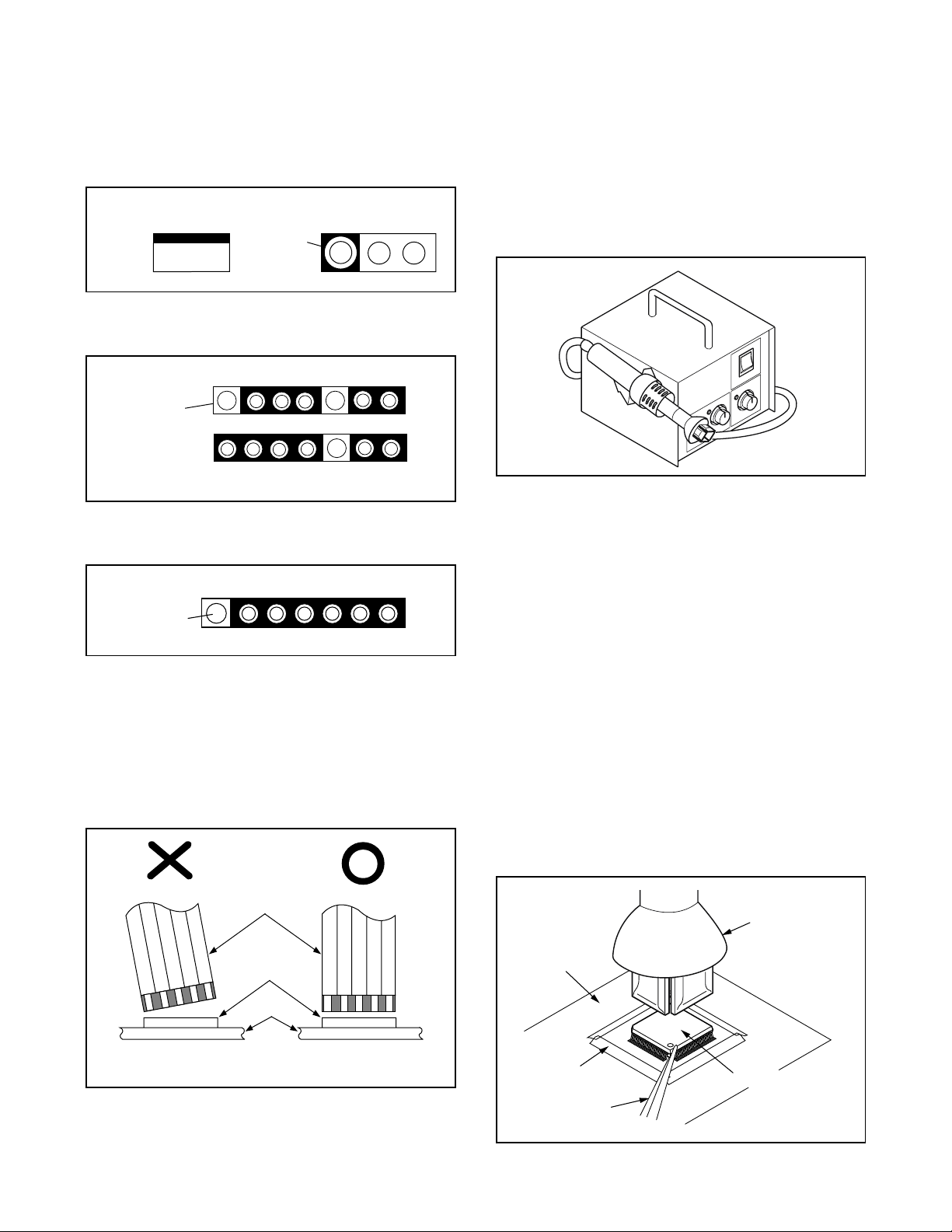
How to Remove / Install Flat Pack-IC
1. Removal
With Hot-Air Flat Pack-IC Desoldering Machine:.
(1) Prepare the hot-air flat pack-IC desoldering
machine, then apply hot air to the Flat Pack-IC
(about 5 to 6 seconds). (Fig. S-1-1)
Fig. S-1-1
(2) Remove the flat pack-IC with tweezers while apply-
ing the hot air.
(3) Bottom of the flat pack-IC is fixed with glue to the
CBA; when removing entire flat pack-IC, first apply
soldering iron to center of the flat pack-IC and heat
up. Then remove (glue will be melted). (Fig. S-1-6)
(4) Release the flat pack-IC from the CBA using twee-
zers. (Fig. S-1-6)
Instructions for Connectors
1. When you connect or disconnect the FFC (Flexible
Foil Connector) cable, be sure to first disconnect
the AC cord.
2. FFC (Flexible Foil Connector) cable should be
inserted parallel into the connector, not at an angle.
FFC Cable
Connector
CBA
* Be careful to avoid a short circuit.
Caution:
1. Do not supply hot air to the chip parts around the
flat pack-IC for over 6 seconds because damage
to the chip parts may occur. Put masking tape
around the flat pack-IC to protect other parts from
damage. (Fig. S-1-2)
2. The flat pack-IC on the CBA is affixed with glue, so
be careful not to break or damage the foil of each
pin or the solder lands under the IC when removing
it.
Hot-air
Flat Pack-IC
Desoldering
CBA
Masking
Tape
Tweezers
Machine
Flat Pack-IC
Fig. S-1-2
1-4-1
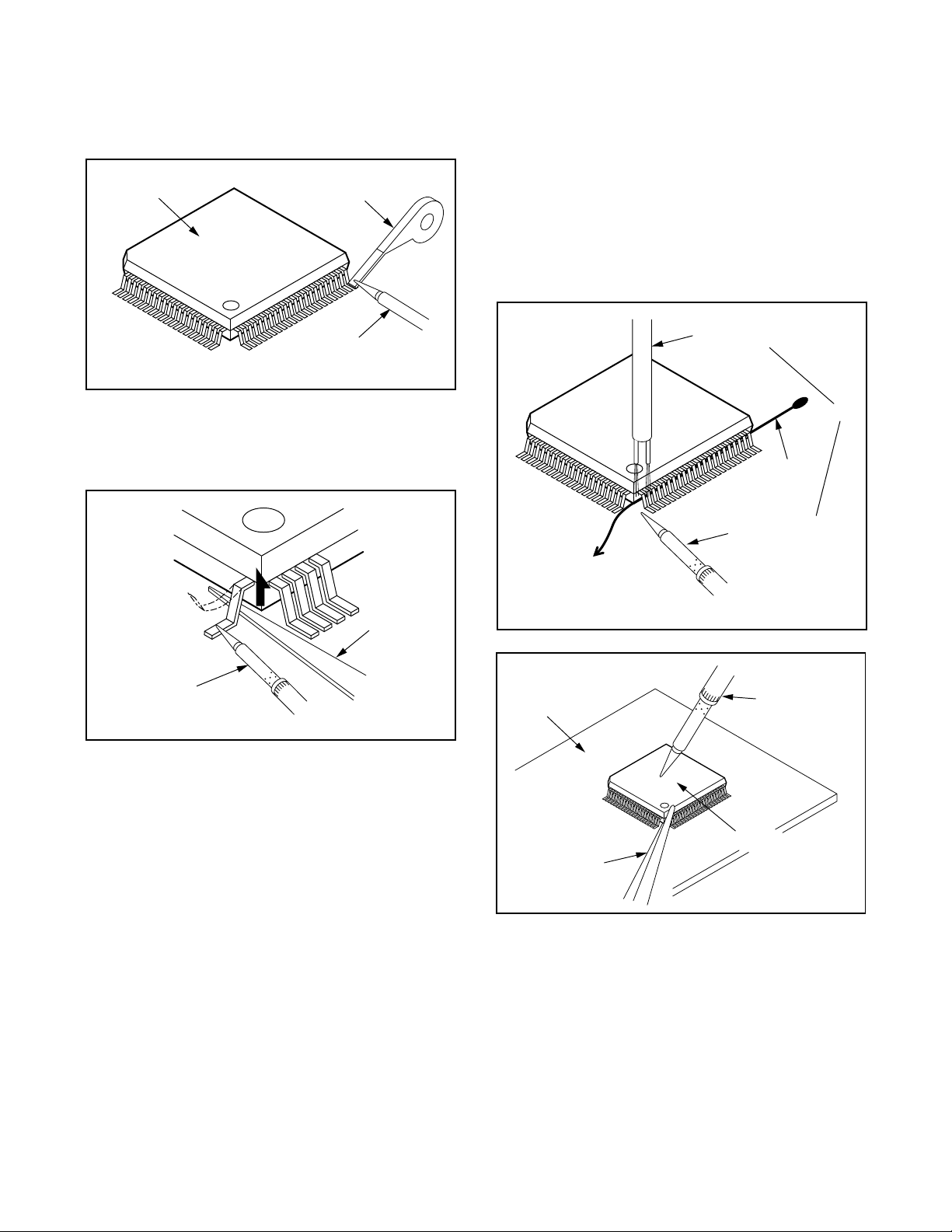
With Soldering Iron:
(1) Using desoldering braid, remove the solder from all
pins of the flat pack-IC. When you use solder flux
which is applied to all pins of the flat pack-IC, you
can remove it easily. (Fig. S-1-3)
Flat Pack-IC
Desoldering Braid
(4) Bottom of the flat pack-IC is fixed with glue to the
CBA; when removing entire flat pack-IC, first apply
soldering iron to center of the flat pack-IC and heat
up. Then remove (glue will be melted). (Fig. S-1-6)
(5) Release the flat pack-IC from the CBA using twee-
zers. (Fig. S-1-6)
Note:
When using a soldering iron, care must be taken
to ensure that the flat pack-IC is not being held by
glue. When the flat pack-IC is removed from the
CBA, handle it gently because it may be damaged
if force is applied.
Soldering Iron
Fig. S-1-3
(2) Lift each lead of the flat pack-IC upward one by
one, using a sharp pin or wire to which solder will
not adhere (iron wire). When heating the pins, use
a fine tip soldering iron or a hot air desoldering
machine. (Fig. S-1-4)
Sharp
Pin
Fine Tip
Soldering Iron
Fig. S-1-4
(3) Bottom of the flat pack-IC is fixed with glue to the
CBA; when removing entire flat pack-IC, first apply
soldering iron to center of the flat pack-IC and heat
up. Then remove (glue will be melted). (Fig. S-1-6)
(4) Release the flat pack-IC from the CBA using twee-
zers. (Fig. S-1-6)
With Iron Wire:
(1) Using desoldering braid, remove the solder from all
pins of the flat pack-IC. When you use solder flux
which is applied to all pins of the flat pack-IC, you
can remove it easily. (Fig. S-1-3)
(2) Affix the wire to a workbench or solid mounting
point, as shown in Fig. S-1-5.
(3) While heating the pins using a fine tip soldering
iron or hot air blower, pull up the wire as the solder
melts so as to lift the IC leads from the CBA contact
pads as shown in Fig. S-1-5
To Solid
Mounting Point
CBA
Tweezers
Hot Air Blower
or
Iron Wire
Soldering Iron
Fig. S-1-5
Fine Tip
Soldering Iron
Flat Pack-IC
Fig. S-1-6
1-4-2
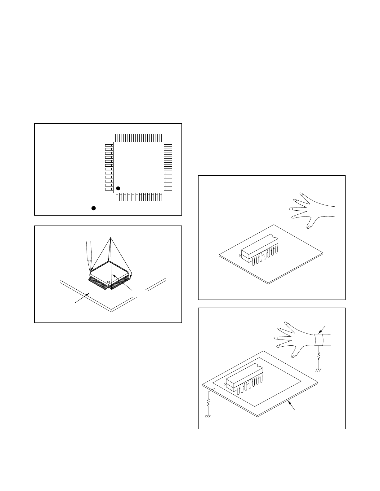
2. Installation
(1) Using desoldering braid, remove the solder from
the foil of each pin of the flat pack-IC on the CBA
so you can install a replacement flat pack-IC more
easily.
(2) The “ I ” mark on the flat pack-IC indicates pin 1.
(See Fig. S-1-7.) Be sure this mark matches the 1
on the PCB when positioning for installation. Then
presolder the four corners of the flat pack-IC. (See
Fig. S-1-8.)
(3) Solder all pins of the flat pack-IC. Be sure that none
of the pins have solder bridges.
Example :
Pin 1 of the Flat Pack-IC
is indicated by a " " mark.
Fig. S-1-7
Instructions for Handling Semi-conductors
Electrostatic breakdown of the semi-conductors may
occur due to a potential difference caused by electrostatic charge during unpacking or repair work.
1. Ground for Human Body
Be sure to wear a grounding band (1MΩ) that is properly grounded to remove any static electricity that may
be charged on the body.
2. Ground for Workbench
Be sure to place a conductive sheet or copper plate
with proper grounding (1MΩ) on the workbench or
other surface, where the semi-conductors are to be
placed. Because the static electricity charge on clothing will not escape through the body grounding band,
be careful to avoid contacting semi-conductors with
your clothing.
< Incorrect >
CBA
Presolder
Flat Pack-IC
Fig. S-1-8
CBA
< Correct >
Grounding Band
1MΩ
CBA
1MΩ
Conductive Sheet or
Copper Plate
1-4-3

PREPARATION FOR SERVICING
How to Enter the Service Mode
About Optical Sensors
Caution:
An optical sensor system is used for the Tape Start
and End Sensors on this equipment. Carefully read
and follow the instructions below. Otherwise the unit
may operate erratically.
What to do for preparation
Insert a tape into the Deck Mechanism Assembly and
press the PLAY button. The tape will be loaded into
the Deck Mechanism Assembly. Make sure the power
is on, TP507 (SENSOR INHIBITION) to GND. This will
stop the function of Tape Start Sensor, Tape End Sensor and Reel Sensors. (If these TPs are connected
before plugging in the unit, the function of the sensors
will stay valid.) See Fig. 1.
Note: Because the Tape End Sensors are inactive, do
not run a tape all the way to the start or the end of the
tape to avoid tape damage.
About REC-Safety Switch
Caution:
The REC-Safety Switch is directly mounted on the
Main CBA. When the Deck Mechanism Assembly is
removed from the Main CBA for servicing, this switch
does not work automatically.
What to do for preparation
In order to record, press the Rec button while pushing
REC-SAFETY SW on the Main CBA. See Fig. 1.
Q503
SW506
Q504
TP507
S-INH
(REC-SAFETY SW)
Fig. 1
1-5-1
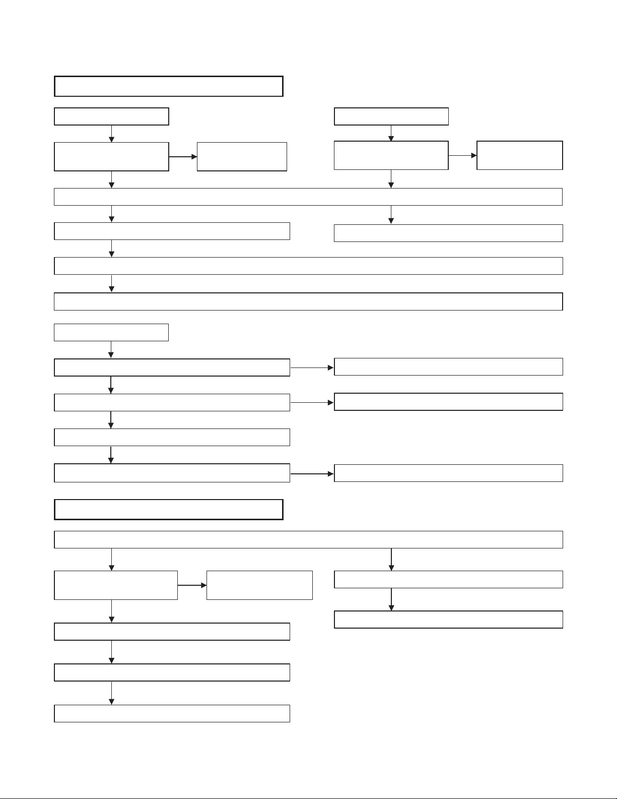
TROUBLESHOOTING
Video problem 1 (No recording Video)
RF INPUT
Check Video signal at pin
48 of IC301.
OK
Check Video signal at pin 65 of IC301 or pin 50 of IC501.
OK
Check Video signal at pin 52 of IC501 or pin 56 of IC301.
OK
Cleaning the Video Head. (See page 2-7-2.)
NG
Check Cylinder Assembly.
LINE INPUT (AV2)
Check Video signal at pin 52 of IC301.
OK
Check Video signal at pin 65 of IC301 or pin 50 of IC501.
OK
NG
Check TU701.
NG
NG
LINE INPUT (AV1)
Check Video signal at pin
50 of IC301.
OK
NG
Check IC301, X301, etc.
Check A/V cable.
Check IC301, X301, etc.
NG
Check A/V cable.
Check Video signal at pin 52 of IC501 or pin 56 of IC301.
OK
Cleaning the Video Head.(See page 2-7-2.)
Video problem 2 (No playback Video)
Check signal at pin 94 and pin 96(or pin 93) of IC301.
OK
Check Video signal at pin 65
of IC301 or pin 50 of IC501.
OK
Check Video signal at pin 52 of IC501 or pin 56 of IC301.
OK
Check Video signal at pin 61 or 63 of IC301.
OK
Check V-OUT jack or TU701.
NG
Check IC301, X301, etc.
NG
Check Cylinder Assembly.
NG
Cleaning the Video Head. (See page 2-7-2.)
OK
Check Cylinder Assembly.
1-6-1
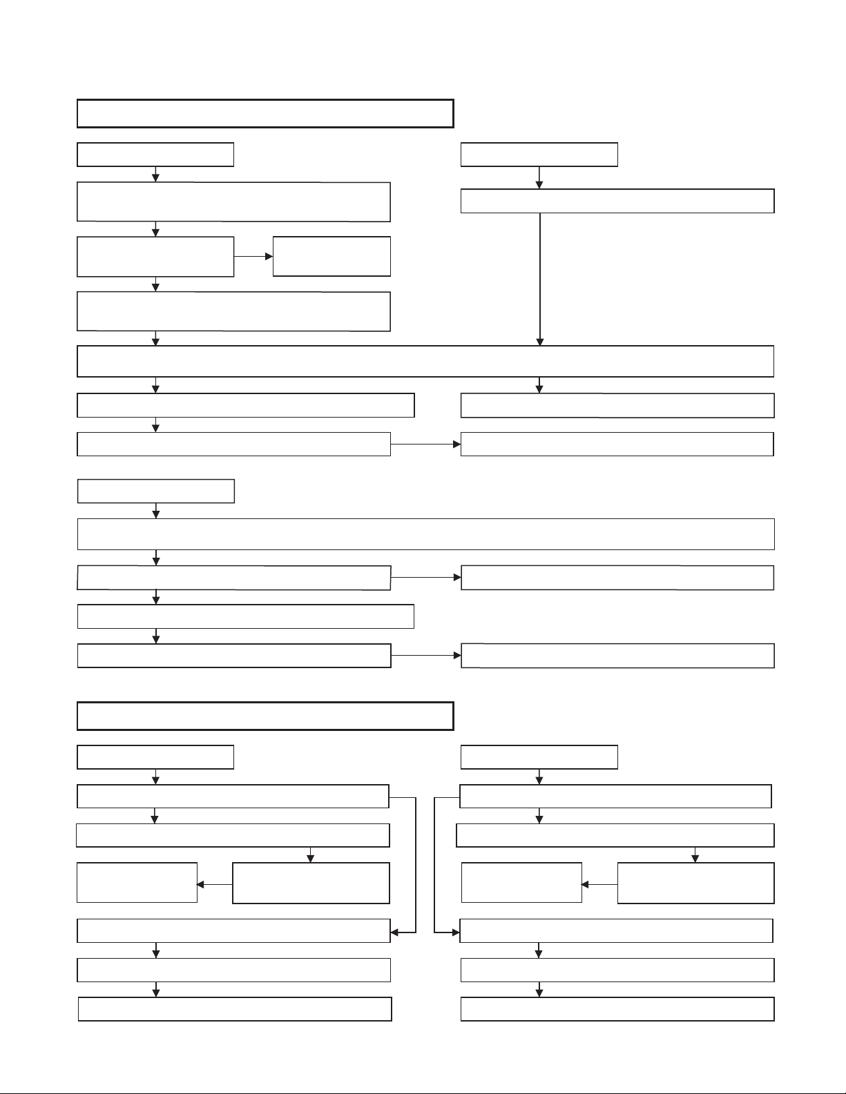
Audio problem 1 (No recording Normal Audio)
RF-INPUT
Change for Audio-mode(MONO) by AUDIO-SELECT
KEY of Remote Controller.
OK
NGCheck SIF signal at pin 2
of CN701.
OK
Check Audio signal at pin 4 and 5 of CN701 or pin 51
and 53 of IC451.
OK
Check Audio signal at pin 6 of IC451 or pin 15 of IC301.
OK
Check Tape interchangeability alignment. (See page 2-6-2.)
NG
Cleaning the Audio Control Head. (See page 2-7-2.)
LINE INPUT (AV2)
Check Audio signal at pin 11(or 67) or pin 73(or 65) of IC451.
OK
Check Audio signal at pin 6 of IC451 or pin 15 of IC301.
OK
Check Tape interchangeability alignment. (See page 2-6-2.)
NG
Cleaning the Audio Control Head. (See page 2-7-2.)
Check TU701,
NICAM unit.
NG
NG
NG
LINE INPUT (AV1)
Check Audio signal at pin 7 or 69 of IC451.
OK
NG
Check IC451, IC301.
Check AC Head Assembly.
Check IC451, IC301.
Check AC Head Assembly.
Audio problem 2 (No playback Normal Audio)
(AV1) (AV2)
Check Audio signal at pin 5 of IC301. Check Audio signal at pin 5 of IC301.
NG
Check Tape interchangeability alignment.
NG
Check the AC Head
Assembly.
Check Audio signal at pin 11 of IC301 or pin 4 of IC451. Check Audio signal at pin 11 of IC301 or pin 4 of IC451.
OK
Check Audio signal at pin 78 and 80 or 2 of IC451. Check Audio signal at pin 75 and 76 of IC451.
OK
Check TU701 or A-OUT jack. Check A-OUT jack.
Cleaning the Audio Control
NG
Head. (See page 2-7-2.)
1-6-2
OKOK
NG
Check Tape interchangeability alignment. (See page 2-6-2.)
NG
Check the AC Head
Assembly.
OK
OK
Cleaning the Audio Control
NG
Head. (See page 2-7-2.)

Audio problem 3 (No recording Hi-Fi Audio)
RF-INPUT
Check SIF signal at pin 2
of CN701.
OK
Check Audio signal at pin 4
and 5 of CN701 or pin 51
and 53 of IC451.
OK
Check signal at pin 26 of IC451.
OK
Cleaning the Video Head. (See page 2-7-2.)
LINE INPUT (AV2)
Check Audio signal at pin 11(or 67) and 73(or 63) of
IC451.
OK
Check signal at pin 26 of IC451.
OK
Cleaning the Video Head. (See page 2-7-2.)
NG NG
Check TU701.
NG
Check NICAM until.
NG
NG
NG
NG
NG
LINE INPUT (AV1)
Check Audio signal at pin
7 and 69 of IC451.
OK
Check signal at pin 26 of IC451.
NG
Cleaning the Video Head.
Check IC451.
Check Cylinder Assembly.
Check A/V cable.
Check IC451.
Check Cylinder Assembly.
(See page 2-7-2.)
Check A/V cable.
OK
NG
Audio problem 4 (No playback Hi-Fi Audio)
(AV1) (AV2)
Check signal at pin 24 and 27 of IC451.
OK
Cleaning the Video Head.
Check Audio signal at pin
78 and 80 of IC451.
OK
Check TU701, A-OUT jack.
NG
Check IC451.
NG
NG
Check Cylinder Assembly.
Check Audio signal at pin
75 and 76 of IC451.
OK
NG
OK
Check IC451.
1-6-3
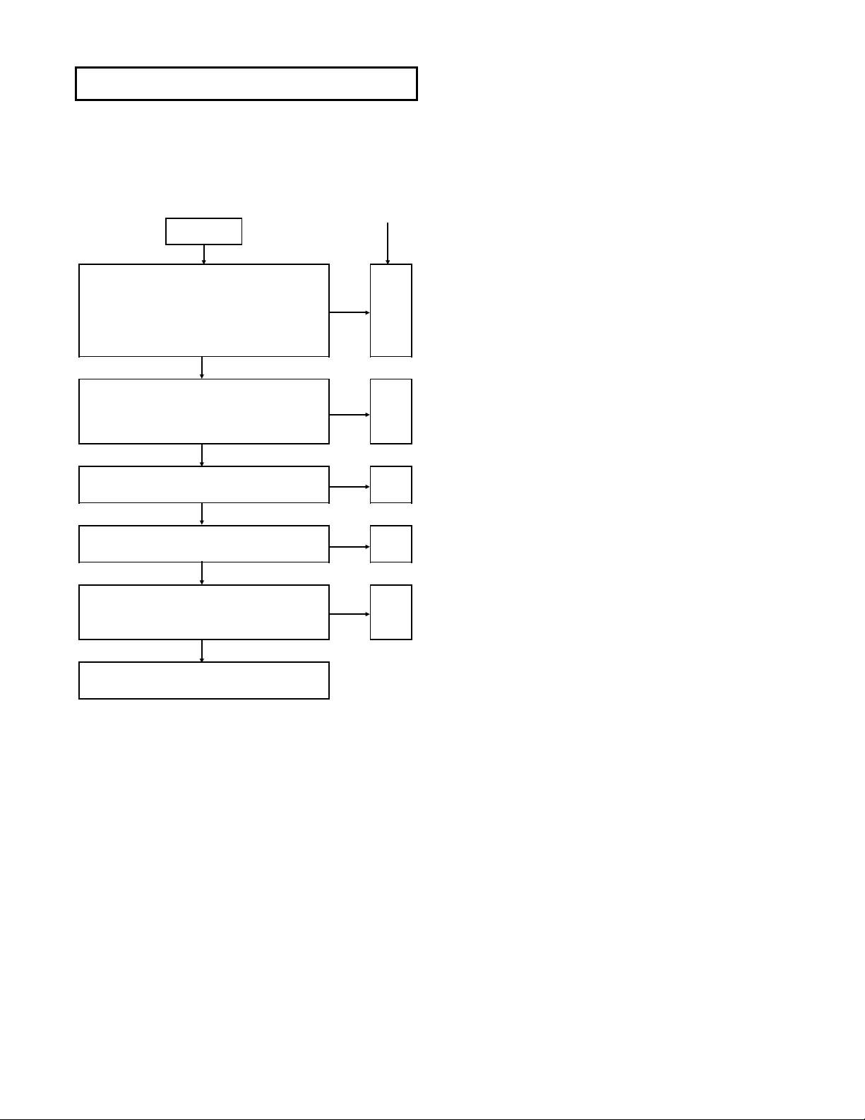
Power problem
It is highly recommended that a variable isolation
transformer which can monitor current be used.
(Alternatively a variable AC source which monitors current will do). Read directions below before
power is added!
2] Check for any defective parts while the secondary
rectifying diodes are disconnected (D011, D013 and
D014) perform a diode check in both forward and
reverse directions through a tester.
3] Remove the following components and check for
defects: snubber diode (D005), switching FET (Q001),
source resistor (R006), control transistor (Q002).
Repair method
CHECK
Connect unit to the isolation transformer and slowly increase the AC supply while monitoring the current, if it
draws too much current (Be ware fuse
is rated for 1.6 amps), then turn off
supply and do repair method #1.
NO
Check whether the primary rectifying
DC of the Switching power supply has
an output. (Reading should be about
168V.)
YES
With the primary DC working check
the secondary 5V.
YES
Are the 44V, 12V and 5V
higher than normal?
NO
Although the secondary 5V is working,
are any of the other voltages higher
than normal (44V and 12V)?
NO
There is no problem on the SW power
supply.
YES
NO
NO
YES
YES
#1
#2
#3
#4
#5
Repair method #1
(Power must be off)
Short circuit in the secondary side. check diode D014,
D011, D012, D013, switching FET (Q001), control
transistor (Q002), diode (D006), and resistor (R014)
replace as necessary.
Disconnect 44V diode (D011), 12V diode (D013), 5V
diode (D014). Check the load continuity of 44V line,
12V line and 5V line through a tester (resistance
range).
If the tester indicates a lower resistance value around
0 ohm, the line is short-circuited.
Before repairing the switching power supply, find out
the short-circuited area of such line and repair it.
If the tester does not indicate any low resistance value
(around 0 ohm), no load is short-circuited and there is
no problem.
Repair method #2
Check the fuse 1.6A (F001), primary rectifying diodes
(D001-D004) as possible problems. Remove the
above mentioned parts and check them. The circuit
which turns on switching FET (Q001) may be
regarded as a possible cause, even if the load at the
secondary side is shorted, it can't be detected
because switching FET (Q001) isn't operating. Perform check according to the step 1 and 2 of repair
method #1 and check the following parts:
(Remove the part from PCB)
Switching FET (Q001), source resistor (R006), gate
resistor (R008) and start resistor (R004 and R005).
Repair method #3
A circuit to turn on switching FET (Q001) may not work
and this may be regarded as a cause of trouble. Even
if the load at the secondary side is short-circuited, it
cannot be detected because switching FET (Q001)
does not turn on. Therefore, perform check according
to the steps 1] and 2] of the repair method #1 and execute the under-mentioned parts breakage check.
(Remove the part from PCB.)
switching FET (Q001), source resistor (R014), control
transistor (Q002), gate resistor (R005) and start resistor (R003, R004 and R028).
Repair method #4
The feedback circuit which is monitored by the output
of voltage may not work and this may be regarded as
a possible cause, remove control transistor Q002 and
check for defects. More over, a photo coupler (IC001)
and transistor (Q004) may be defective, replace any
defective parts with factory originals.
Repair method #5
If the output voltage of the secondary side is slightly
high, the line load may be in the "OPEN" state and this
may be regarded as a cause of trouble. If there is no
output voltage on the secondary side, the rectifying
diodes (D014), (D013) may be defective.
1-6-4
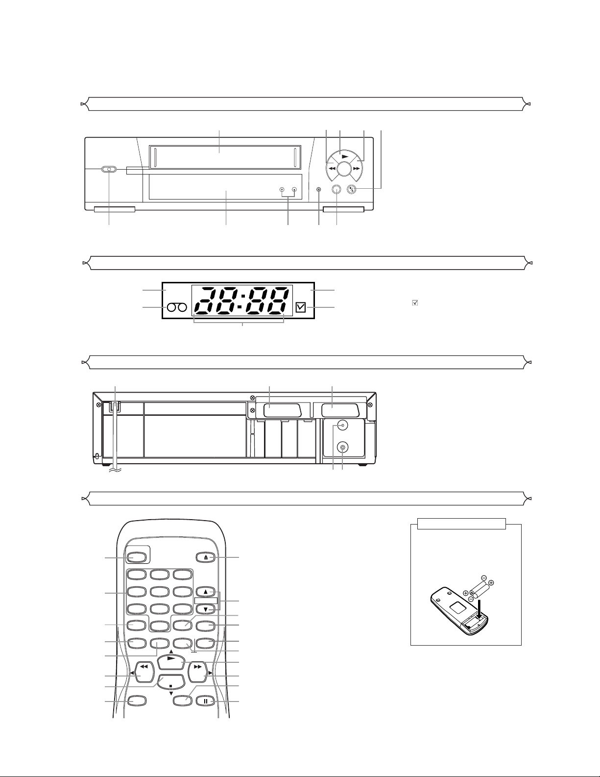
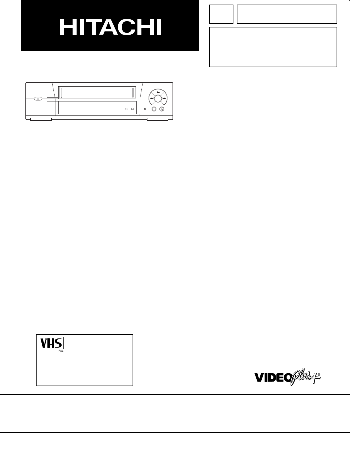
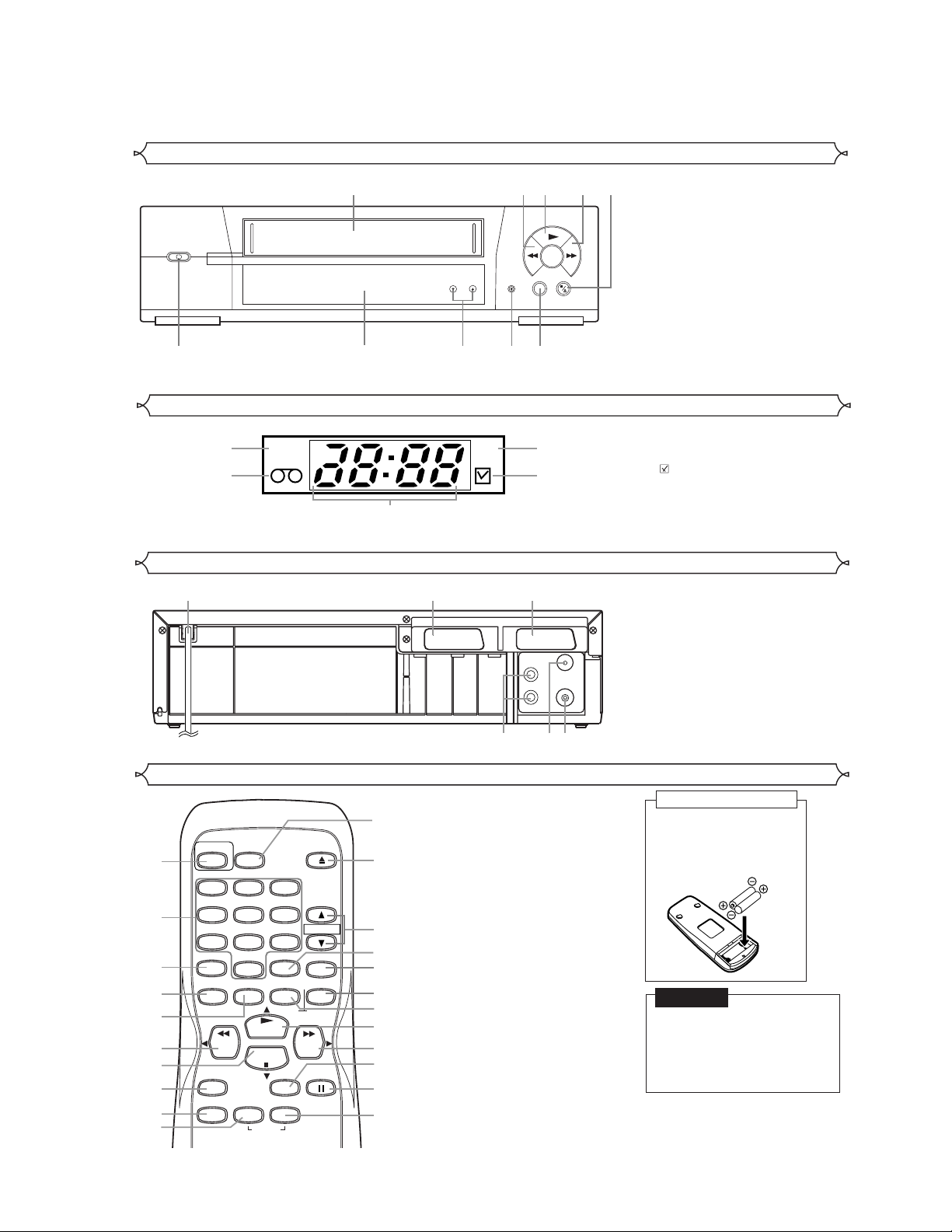
OPERATING CONTROLS AND FUNCTIONS
VT-MX210EUK
Front Panel
1. Cassette compar tment
2. E (REW) button
3. B (PLAY) button
4. D (F.FWD) button
5.
C/A (STOP/EJECT) button
6. k (PAUSE) button
7. REC button
8. CHANNEL (o/p) [TRACKING]
buttons
9. Indicator (See below)
10.y (STANDBY) button
11. PWR. (Power) indicator
12. TAPE IN indicator
13. REC indicator
14. (Timer) indicator
15. CLOCK indicator
Indicator
11
12
12435
PWR. REC
15
678910
13
14
Rear Panel
16
Remote Control
STANDBY
1
1
2
4
7
VIDEO Plus+
3
DISPLAY
4
MENU
5
EW
6
7
R
REC
8
2
5
8
0
PLAY
STOP
3
6
9
DAILY/WEEKLY
RESET
SPEED
EJECT
CHANNEL
SLOW
COUNTER
MEMORY
D
W
F. F
PAUSE/STILL
18
17
16
15
14
13
12
11
10
9
1817
AV2(DECODER) AV1(TV)
AERIAL
RF OUT
1920
1. STANDBY button
2. NUMBER buttons
3. VIDEO Plus+ button
4. MENU button
5. DISPLAY button
6. REW button
7. STOP button
8. REC button
9. PAUSE/STILL button
10. SPEED button
11. F.FWD button
12. PLAY button
13. COUNTER RESET button
14. COUNTER MEMORY button
15. SLOW button
16. DAILY/WEEKLY button
17. CHANNEL (o/p) buttons
18. EJECT button
16. Power cord
17. AV2 (DECODER) socket
18. AV1 (TV) socket
19. RF OUT socket
20. AERIAL socket
To insert the batteries:
Install two AA batteries
matching the polarity indicated inside the battery
compartment.
1-7-1
Front Panel
Indicator
11
12
Rear Panel
16
VT-FX240EUK
12435
PWR. REC
15
AV2(DECODER) AV1(TV)
1817
AUDIO
OUTPUT
678910
13
14
1. Cassette compar tment
2. E (REW) button
3. B (PLAY) button
4. D (F.FWD) button
5.
C/A (STOP/EJECT) button
6. k (PAUSE) button
7. REC button
8. CHANNEL (o/p) [TRACKING]
buttons
9. Indicator (See below)
10.y (STANDBY) button
11. PWR. (Power) indicator
12. TAPE IN indicator
13. REC indicator
14. (Timer) indicator
15. CLOCK indicator
16. Power cord
17. AV2 (DECODER) socket
18. AV1 (TV) socket
19. RF OUT socket
20. AERIAL socket
L
AERIAL
RF OUT
R
21. AUDIO OUTPUT L/R jacks
1-7-2
Remote Control
STANDBY
1
1
2
4
7
VIDEO Plus+
3
4
MENU
5
6
7
8
R
REC
QUICK-FIND
9
10
EW
AUDIO
SELECT
2
5
8
0
DISPLAY
STOP
TIME
SEARCH
PLAY
3
6
9
DAILY/WEEKLY
RESET
SPEED
INDEX
EJECT
CHANNEL
SLOW
COUNTER
MEMORY
D
W
F. F
PAUSE/STILL
22
21
20
19
18
17
16
15
14
13
12
11
192021
1. STANDBY button
2. NUMBER buttons
3. VIDEO Plus+ button
4. MENU button
5. DISPLAY button
6. REW button
7. STOP button
8. REC button
9. QUICK-FIND button
10. TIME SEARCH button
11. INDEX SEARCH button
12. PAUSE/STILL button
13. SPEED button
14. F.FWD button
15. PLAY button
16. COUNTER RESET button
17. COUNTER MEMORY button
18. SLOW button
19. DAILY/WEEKLY button
20. CHANNEL (o/p) buttons
21. EJECT button
22. AUDIO SELECT button
To insert the batteries:
Install two AA batteries
matching the polarity indicated inside the battery
compartment.
CAUTION
On Battery Replacement
• Do not mix old and new
batteries. (Also never mix alka-
line batteries with manganese
batteries.)
CHAPTER 2 DISASSEMBLY AND ADJUSTMENT
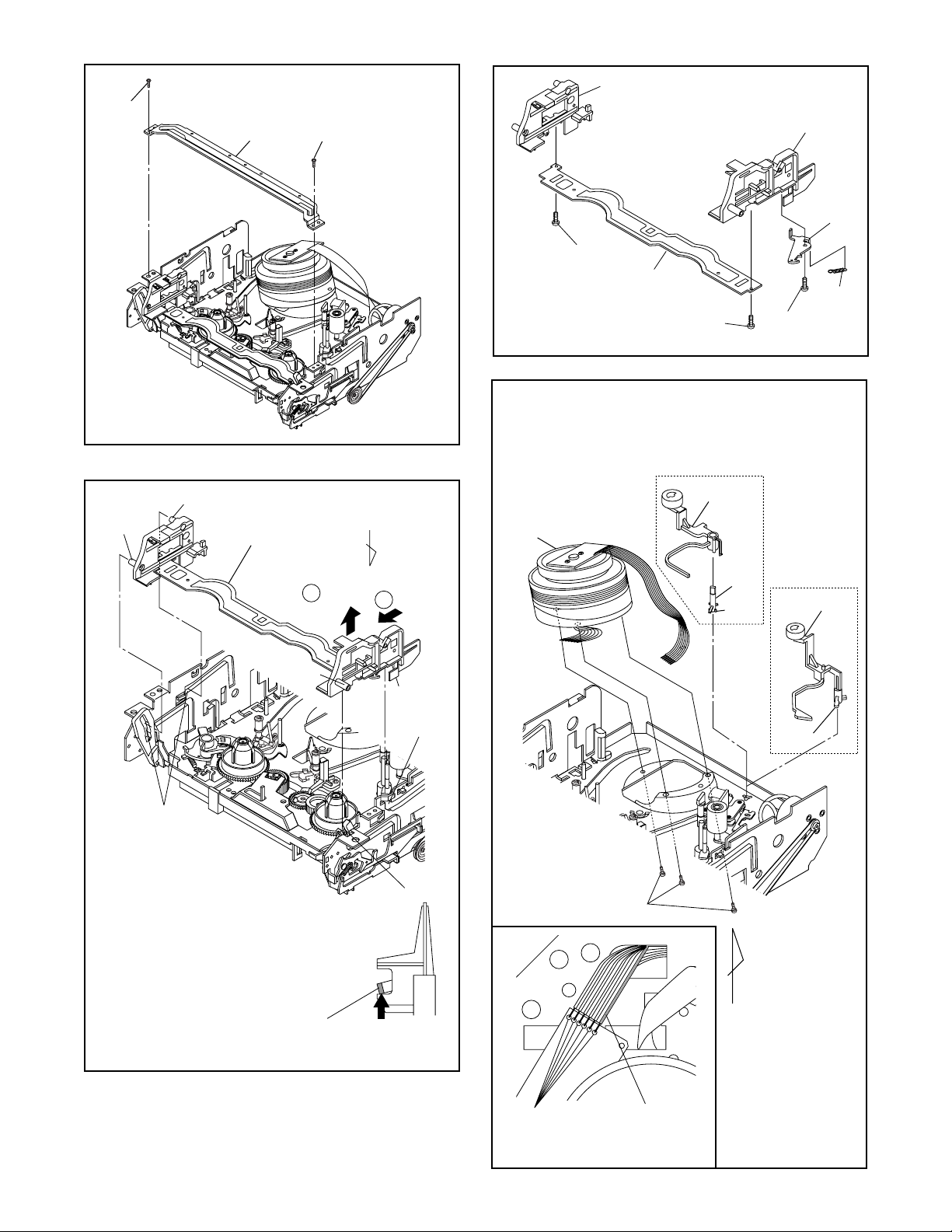
CABINET DISASSEMBLY INSTRUCTIONS
1. Disassembly Flowchart
This flowchart indicates the disassembly steps to gain
access to item(s) to be serviced. When reassembling,
follow the steps in reverse order. Bend, route, and
dress the cables as they were originally.
[1] Top Case
[2] Front Assembly
[3] VCR Chassis Unit
[4] Jack CBA
[5] Function CBA
[6] Deck Assembly
[7] Main CBA
2. Disassembly Method
REMOVAL
ID/
LOC.
No.
PART
REMOVE/*UNHOOK/
Fig.
UNLOCK/RELEASE/
No.
UNPLUG/DESOLDER
Note
(1): Identification (location) No. of parts in the figures
(2): Name of the part
(3): Figure Number for reference
(4): Identification of parts to be removed, unhooked,
unlocked, released, unplugged, unclamped, or
desoldered.
P=Spring, L=Locking Tab, S=Screw,
CN=Connector
*=Unhook, Unlock, Release, Unplug, or Desolder
e.g. 2(S-2) = two Screws (S-2),
2(L-2) = two Locking Tabs (L-2)
(5): Refer to “Reference Notes.”
Reference Notes
CAUTION: Locking Tabs (L-1) and (L-2) are fragile.
Be careful not to break them.
1. Release Locking Tab (L-3) and remove Screw
(S-2), five Screws (S-3), three Screws (S-4) and
Screw (S-5). Then, slowly lift the VCR Chassis Unit
(Deck Assembly, Function CBA, Jack CBA and
Main CBA) up.
2. When reassembling, solder wire jumpers as shown
in Fig. 5.
3. Before installing the Deck Assembly, be sure to
place the pin of LD-SW on Main CBA as shown in
Fig. 6. Then, install the Deck Assembly while aligning the hole of Cam Gear with the pin of LD-SW,
the shaft of Cam Gear with the hole of LD-SW as
shown in Fig. 6.
[1] Top Case 1 7(S-1) -
Front
[2]
Assembly
VCR
[3]
Chassis
Unit
[4] Jack CBA 4 Desolder, (S-6) -
Function
[5]
CBA
Deck
[6]
Assembly
[7] Main CBA 5 ---------- -
↓
(1)
↓
(2)
2 *3(L-1),*4(L-2) -
*(L-3), (S-2), 5(S-3),
3
3(S-4), (S-5)
5 Desolder -
5,6 2(S-7), Desolder 2,3
↓
(3)
↓
(4)
1
↓
(5)
2-1-1
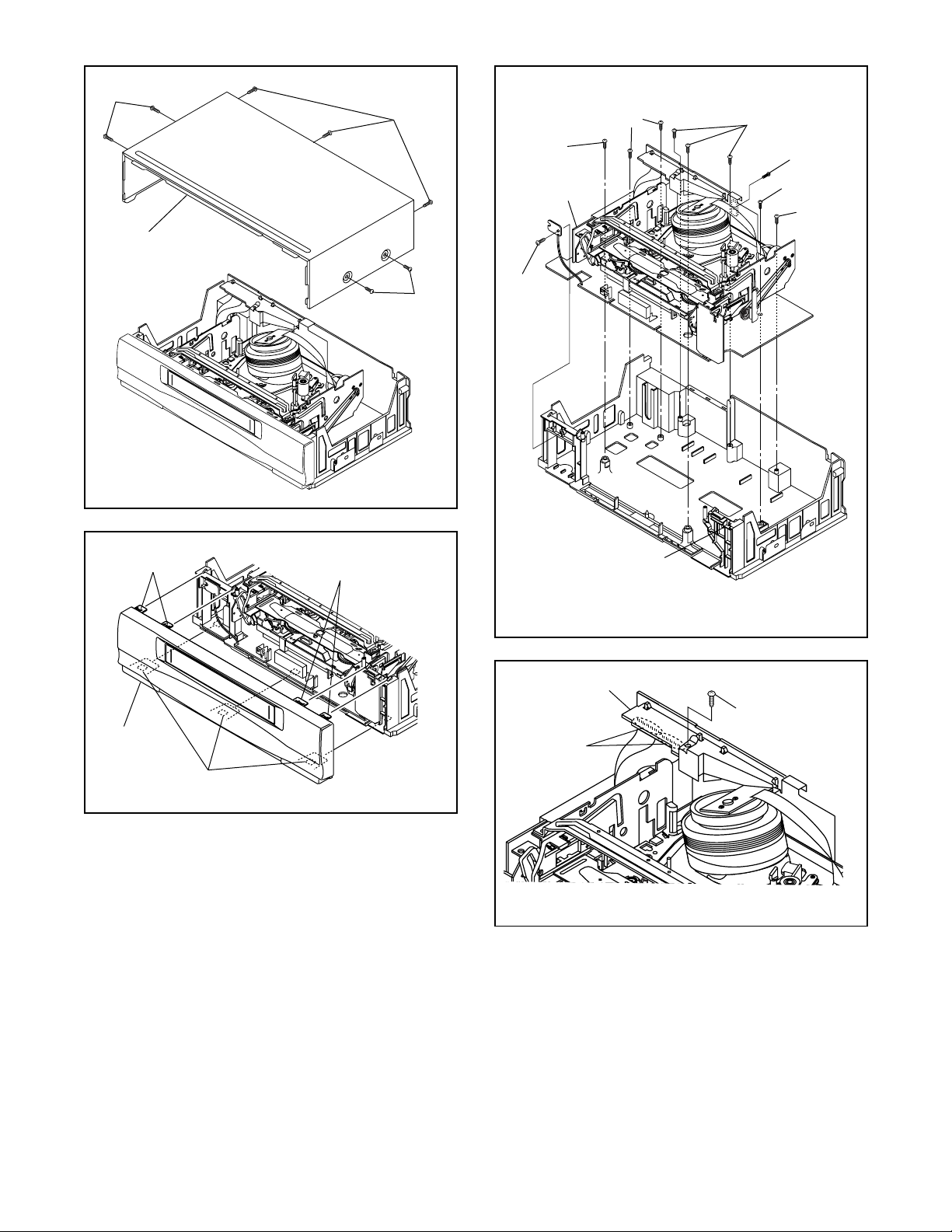
(S-1)
[1] Top Case
(S-1)
(S-1)
Fig. 1
(S-3)
[3]VCR
Chassis Unit
(S-2)
(S-4)
(S-3)
(S-5)
(S-4)
(S-3)
(L-2)
[2] Front
Assembly
(L-1)
(L-3)
(L-2)
Fig. 3
[4] Jack CBA
(S-6)
Desolder
Fig. 2
Fig. 4
2-1-2

FE Head
Cylinder Assembly
AC Head
Assembly
Pin
SW507
LD-SW
[6] Deck Assembly
(S-7)
[5] Function
CBA
From
FE Head
Lead with
red stripe
From
Cylinder
Assembly
Lead with
white stripe
From
AC Head
Assembly
[7] Main CBA
Desolder
From
Capstan Motor
Assembly
Lead with
white stripe
(S-7)
[7] Main CBA
[6] Deck Assembly
Shaft
Hole
LD-SW
Cam Gear
Hole
Pin
[7] Main CBA
Fig. 6
TOP VIEW
Lead connections of Deck Assembly and Main CBA
Fig. 5
2-1-3
DISASSEMBLY/ASSEMBLY PROCEDURES
OF DECK MECHANISM
Before following the procedures described below, be sure to remove the deck assembly from the cabinet. (Refer to
CABINET DISASSEMBLY INSTRUCTIONS on page 2-1-1.)
All the following procedures, including those for adjustment and replacement of parts, should be done in Eject
mode; see the positions of [41] and [42] in Fig.DM1 on page 2-2-3. When reassembling, follow the steps in reverse
order.
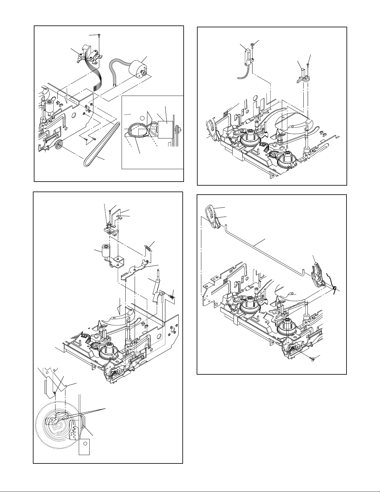
STEP
/LOC.
START-
ING
No.
[1] [1]
[2] [1]
[3] [2] Slider L T DM5 (S-2)
[4] [2] Slider R T DM5 (S-3)
[5] [4]
[6] [2]
[7] [7] Cylinder Assembly T DM1,DM6 Desolder, 3(S-5)
[8] [8] Loading Motor Assembly T DM1,DM7
[9] [9]
[10] [2]
[11] [10]
[12] [11] Pinch Arm (B) T DM1,DM8 *(P-3)
[13] [12]
[14] [14]
[15] [15]
[16] [2] Slider Shaft T DM10 (S-11),*(L-3)
[17] [16]
[18] [16]
[19] [7],[10]
[20] [20] Clutch Assembly(HI) B DM2,DM12 (C-1)
[21] [20]
[22] [22]
[23] [22]
[24] [24] Mode Gear B DM2,DM14 (C-4)
[25]
[26] [22] Worm Holder B DM2,DM14 (S-15)
[27] [26] Pulley Assembly B DM2,DM14
[28] [22],[25]
[29] [20]
[30] [29] TR Gear Spring B DM14
[31] [30] TR Gear A/B B DM1,DM14
[32] [31]
[33] [21],[25]
[34] [25] BT Arm B DM2,DM15 *(P-5)
No.
[20],[23],
[24]
Guide Holder A T DM3 2(S-1)
Cassette Holder Assembly T DM4
Lock Lever T DM5 (S-4),*(P-1)
C Plate T DM5
AC Head Assembly T DM1,DM7 (S-7)
Tape Guide Assembly T DM1,DM8 *(P-2)
Door Opener B T DM1,DM8 *(L-1),*(L-2)
Pinch Arm (A) Assembly T DM1,DM8
FE Head T DM1,DM9 (S-9)
Prism T DM1,DM9 (S-10)
C Drive Lever L T DM10
C Drive Lever R T DM10
Capstan Motor B DM2,DM11 3(S-12), Cap Belt
Center Gear B DM12
Cam Holder F B DM2,DM13 (C-2)
Cam Gear (B) B DM2,DM13 (C-3),*(P-4)
Mode Lever(HI) B DM2,DM14 (C-5), *(L-4)
Cam Gear (A) B DM2,DM14
TR Gear C B DM2,DM14 (C-6)
FF Arm(HI) B DM1,DM14
Idler Assembly(HI) B DM1,DM15 *(L-5)
PART
Fig. No.
REMOVAL INSTALLATION
REMOVE/*UNHOOK/
UNLOCK/RELEASE/
UNPLUG/DESOLDER
Desolder, LDG Belt,
2(S-6)
ADJUSTMENT
CONDITION
(+)Refer to Alignment
Sec.Pg.2-3-2
2-2-1
STEP
/LOC.
START-
ING
No.
[35] [25]
[36] [35]
[37] [2],[25]
[38] [2],[25] M Brake S(HI) Assembly T DM1,DM16 *(P-7)
[39] [38]
[40] [39]
[41] [2]
[42] [2],[15] Sensor Gear T DM1,DM16 (C-8)
[43] [37],[41] Reel T T DM1,DM16
[44] [39]
[45] [35],[38]
[46] [36]
[47] [19] TG Post Assembly T DM1,DM17 *(L-7)
[48] [18],[28]
[49] [48]
[50] [50] Cleaner Lever Assembly T DM1,DM6
[51] [50] CL Post T DM6 *(L-9) Type A
↓
(1)
No.
Loading Arm S(B)
Assembly
Loading Arm T(B)
Assembly
M Brake T(HI) Assembly T DM1,DM16 *(P-6)
Tension Lever Sub
Assembly
T Lever Holder T DM1,DM16 *(L-6)
M Gear(HYT) T DM1,DM16 (C-7)
Reel S T DM1,DM16
Moving Guide S
Preparation
Moving Guide T
Preparation
Rack Assembly R DM18
F Door Opener R DM18
↓
(2)
PART
↓
(3)
Fig. No.
B DM2,DM15
B DM2,DM15
T DM1,DM16
T DM1,DM17
T DM1,DM17
↓
(4)
↓
(5)
REMOVAL INSTALLATION
REMOVE/*UNHOOK/
UNLOCK/RELEASE/
UNPLUG/DESOLDER
(+)Refer to Alignment
Sec.Pg.2-3-1
(+)Refer to Alignment
Sec.Pg.2-3-1
(+)Refer to Alignment
Sec.Pg.2-3-2
Type A
*(L-8) Type B
↓
(6)
ADJUSTMENT
CONDITION
↓
(7)
(1): Follow steps in sequence. When reassembling, follow the steps in reverse order.
These numbers are also used as ldentification (location) No. of parts in the figures.
(2): Indicates the part to start disassembling with in order to disassemble the part in column (1).
(3): Name of the part
(4): Location of the part: T=Top B=Bottom R=Right L=Left
(5): Figure Number
(6): Identification of parts to be removed, unhooked, unlocked, released, unplugged, unclamped, or desoldered.
P=Spring, W=Washer, C=Cut Washer, S=Screw, *=Unhook, Unlock, Release, Unplug, or Desolder
e.g., 2(L-2) = two Locking Tabs (L-2).
(7): Adjustment Information for Installation
(+):Refer to Deck Exploded Views for lubrication.
.
* In case of some models, the Cleaner Lever Assembly and CL Post is not used.
2-2-2
Top View
[14]
[39]
[7] [50] [8]
[46][45] [47][9]
[13]
[11]
[15]
[40]
[38]
Bottom View
[10]
[12]
[37]
[33][44] [42] [31] [32] [41] [43]
Fig. DM1
[19]
[36]
[35]
2-2-3
[26]
[27]
[23]
[28]
[24]
[25]
[34][20][29][22]
Fig. DM2
(S-1)
[1]
(S-1)
Fig. DM3
[3]
[4]
[5]
(S-2)
[6]
(P-1)
(S-3)
(S-4)
Fig. DM5
Note: Either of two types (A and B) of CLEANER
ASSEMBLY is applied for the Deck Assembly. Though
these structures are different, they are compatible.
Pin D
Pin C
Slots B
First, while pushing the locking tab as
shown in the right, slide and pull up the right
side on [2] to release Pin A and Pin B from
the slots A.
Then, remove Pin C and Pin D on [2] from
the slots B as shown.
[2]
Pin A
2
Pull up
A
1
Slide
Pin B
Slot A
Slot A
[7]
Type A
(S-5)
[50]
[51]
(L-9)
Type B
[50]
(L-8)
A
Locking tab
View for A
Fig. DM4
Desolder
from bottom
View for A
Lead with
Blue Stripe
Fig. DM6
2-2-4
[9]
A
(S-7)
(S-6)
(L-2)
LDG
Belt
Adj. Screw
[8]
Desolder
from bottom
Lead with White Stripe
View for A
[8]
Fig. DM7
[11]
(L-1)
[14]
[17]
(L-3)
(S-9)
(S-10)
[15]
Fig. DM9
After removing the Screw (S-11),
while pressing the Locking Tab
(L-3), remove [16].
Pin of [12]
Pin of [10]
[13]
[10]
A
Grooves of [28]
(P-3)
[12]
[16]
[18]
(P-2)
(S-11)
Fig. DM10
2-2-5
View for A
When reassembling [10] and
[12], confirm that pin of [10]
and pin of [12] are in the
[28]
grooves of [28] as shown.
Fig. DM8
Cap Belt
(C-1)
[20]
[19]
[21]
Fig. DM12
(S-12)
Fig. DM11
2-2-6

[23]
(P-4)
(C-3)
(C-2)
(P-4)
[28]
[22]
[27]
[28]
[26]
(S-15)
[25]
(L-4)
(C-6)
[29]
[30]
[31]
(C-5)
(C-4)
[24]
Pin on
bottom
of [23]
Top View
When installing [23], install
the spring (P-4) to [28] as
shown in the left figure, and
then install [23] while
pressing the spring (P-4) to
the direction of the arrow in
the left figure and confirming
that the position of the
spring (P-4) is placed as
shown in the left figure.
[23]
Position of pin on [22]
Pin on [22]
[28]
Fig. DM13
[32]
Pin of [37]
Bottom View
Top View
Position of Mode Lever when installed
Pin of [34]
[28]
Align [25] and [28] as shown.
First groove on [28]
First tooth on [48]
[28]
When reassembling [28],
meet the first groove on
[28] to the first tooth on
[48] as shown.
Pin of [38]
[25]
Fig. DM14
2-2-7

Refer to the Alignment Section, Page 2-3-1.
(P-5)
[45]
[46]
[47]
[34]
[38]
(P-7)
turn
[40]
[33]
(L-6)
turn
[44]
[42]
(L-5)
[39]
(C-8)
[36]
(C-7)
[41]
[35]
Fig. DM15
[43]
(P-6)
[37]
[49]
[48]
(L-7)
Fig. DM17
Slide
Fig. DM18
turn
Fig. DM16
2-2-8

ALIGNMENT PROCEDURES OF MECHANISM
The following procedures describe how to align the
individual gears and levers that make up the tape
loading/unloading mechanism. Since information
about the state of the mechanism is provided to the
System Control Circuit only through the Mode Switch,
it is essential that the correct relationship between
individual gears and levers be maintained.
All alignments are to be performed with the mechanism in Eject mode, in the sequence given. Each
procedure assumes that all previous procedures have
been completed.
IMPORTANT:
If any one of these alignments is not performed
properly, even if off by only one tooth, the unit will
unload or stop and it may result in damage to the
mechanical or electrical parts.
Alignment points in Eject Position
Top View
Alignment [a]
Alignment 3
Alignment 1
Loading Arm, S and T Assembly
Install Loading Arm S and T Assembly so that their
triangle marks point to each other as shown in Fig.
AL2.
Alignment 2
Mode Gear
Keeping the two triangles pointing at each other,
install the Loading Arm T Assembly so that the last
tooth of the gear meets the most inside teeth of the
Mode Gear. See Fig. AL2.
Alignment 1
Triangle Marks
Loading Arm
T Assembly
Loading Arm
S Assembly
Last Tooth
Alignment 2
Most inside teeth
of Mode Gear
Mode Gear
Bottom View
Alignment [a] can be done independently of any
other alignment.
Alignment 1
Alignment 2
Fig. AL1
Fig. AL2
Alignment [a]
Tape Guide Assembly
Measurement of the screw must be as specified in
Fig. AL3.
Tape Guide
Assembly
Screw
3.25 ± 0.1 mm
0.128 ± 0.004 inch
This alignment can be
done independently of
any other alignment.
Fig. AL3
2-3-1

Alignment 3
Cam Gear (A), Rack Assembly
Install the Rack Assembly so that the first tooth on
the gear of the Rack Assembly meets the first
groove on the Cam Gear (A) as shown in Fig. AL4.
Top View
First groove
on the Cam Gear (A)
Cam Gear (A)
Alignment 3
First tooth
Gear on Rack Assembly
Fig. AL4
2-3-2

ELECTRICAL ADJUSTMENT INSTRUCTIONS
General Note: "CBA" is an abbreviation for
"Circuit Board Assembly."
NOTE:
1.Electrical adjustments are required after replacing
circuit components and certain mechanical parts.
It is important to do these adjustments only after
all repairs and replacements have been completed. Also, do not attempt these adjustments
unless the proper equipment is available.
2.To perform these alignment / confirmation procedures, make sure that the tracking control is set in
the center position: Press either "L5??" or "K" button
on the remote control unit first, then the "PLAY"
button (Front Panel only).
Test Equipment Required
1.Oscilloscope: Dual-trace with 10:1 probe,
V-Range: 0.001~50V/Div.,
F-Range: DC~AC-20MHz
2.Alignment Tape (MH-2)
Head Switching Position Adjustment
Purpose:
To determine the Head Switching point during
playback.
Symptom of Misadjustment:
May cause Head Switching noise or vertical jitter
in the picture.
Test point Adj.Point Mode Input
TP751(V-OUT)
TP502(RF-SW)
GND
Tape
MH-2 Oscilloscope
Connections of Measurement Equipment
TP751
Main CBA
TP502
VR501
(Switching Point)
(MAIN CBA)
Measurement
Equipment
GND
PLAY
(SP)
6.5H±1H
(412.7µs±60µs)
Oscilloscope
-----
Spec.
CH1 CH2
Trig. (+)
Figure 1
EXT. Syncronize Trigger Point
V-Sync
CH1
CH2
Reference Notes:
Play back the Alignment tape and adjust VR501 so
that the V-sync front edge of the CH1 video output
waveform is at the 6.5H(412.7µs) delayed position
from the rising edge of the CH2 head switching pulse
waveform.
1.0H
6.5H
Switching Pulse
0.5H
2-4-1

FIXTURE AND TAPE FOR ADJUSTMENT
1. Alignment Tape
No. 7099052 (MH-2)
2. Special Driver
No. 7099028
How To Use The Fixtures And Tape
Item No. Name Part No. Adjustment
1 Alignment Tape 7099052
2 Special Driver 7099028 I Guide Roller
I Head Switching Point
I Tape Interchangeability Alignment
2-5-1

MECHANICAL ALIGNMENT PROCEDURES
Explanation of alignment for the tape to correctly run
starts on the next page. Refer to the information below
on this page if a tape gets stuck, for example, in the
mechanism due to some electrical trouble of the unit.
Service Information
A. Method for Manual Tape Loading/Unloading
To load a cassette tape manually:
1. Disconnect the AC plug.
2. Remove the Top Case and Front Assembly.
3. Insert a cassette tape. Though the tape will not be
automatically loaded, make sure that the cassette
tape is all the way in at the inlet of the Cassette
Holder. To confirm this, lightly push the cassette
tape further in and see if the tape comes back out,
by a spring motion, just as much as you have
pushed in.
4. Turn the LDG Belt in the appropriate direction
shown in Fig. M1 for a minute or two to complete
this task.
To unload a cassette tape manually:
1. Disconnect the AC plug.
2. Remove the Top Case and Front Assembly.
3. Make sure that the Moving guide preparations are
in the Eject Position.
4. Turn the LDG Belt in the appropriate direction
shown in Fig. M1 until the Moving guide preparations come to the Eject Position. Stop turning
when the preparations begin clicking or can not be
moved further. However, the tape will be left
wound around the cylinder.
5. Turn the LDG Belt in the appropriate direction continuously, and the cassette tape will be ejected.
Allow a minute or two to complete this task.
B. Method to place the Cassette Holder in the tape-
loaded position without a cassette tape
1. Disconnect the AC Plug.
2. Remove the Top Case and Front Assembly.
3. Turn the LDG Belt in the appropriate direction
shown in Fig. M1. Release the locking tabs shown
in Fig. M1 and continue turning the LDG Belt until
the Cassette Holder comes to the tape-loaded
position. Allow a minute or two to complete this
task.
Top View
Moving guide T preparation
(Eject Position)
Moving guide S preparation
(Eject Position)
Push the tape
to load it.
Push the locking tab gently to unlock
when loading without a cassette.
UNLOAD
/EJECT
LOAD
Side View
LDG Belt
Fig. M1
Bottom View
2-6-1
LDG Belt (B)
UNLOAD
/EJECT
Cam Gear
Fig. M2

1.Tape Interchangeability Algnment
Note:
To do these alignment procedures, make sure that the
Tracking Control Circuit is set to the center position
every time a tape is loaded or unloaded. (Refer to
page 2-6-4, procedure 1-C, step 2.)
Equipment required:
Dual Trace Oscilloscope
VHS Alignment Tape (MH-2)
Guide Roller Adj. Screwdriver
X-Value Adj. Screwdriver
Note: Before starting this Mechanical Alignment, do all
Electrical Adjustment procedures.
Flowchart of Alignment for tape traveling
Loading (Use a blank tape.)
Adjust the height of the Guide Rollers
(Supply side and take-up side).
(Use a blank tape.) (pg. 2-6-3)
1-A
Check to see that the tape is not creasing
and that there is no slack on the supply
and take-up side Guide Rollers.
(Use a blank tape.)
Adjust the X Value for maximum envelope.
(pg. 2-6-3) (Use Alignment Tape.)
Adjust the envelope. (pg. 2-6-4)
Check the envelope.
OK
Adjust the Audio Section.
(Azimuth Alignment) (pg. 2-6-4)
Check the audio output.
OK
1-A
1-B
1-C
1-C
1-D
1-D
Not good
Not good
Not good
Do the final tape-traveling test to see that
the tape runs normally in play mode without creasing or slacking.
OK
Completion
1-A
Check the following:
1. X Value (pg. 2-6-3)
2. Envelope (pg. 2-6-4)
OK
1-B, 1-C
Not good
Adjust the X value and envelope.
1-B, 1-C
2-6-2

1-A. Preliminary/Final Checking and
Alignment of Tape Path
Purpose:
To make sure that the tape path is well stabilized.
Symptom of Misalignment:
If the tape path is unstable, the tape will be damaged.
Note: Do not use an Alignment Tape for this procedure. If the unit is not correctly aligned, the tape may
be damaged.
1. Play back a blank cassette tape and check to see
that the tape runs without creasing at Guide Rollers
[2] and [3], and at points A and B on the lead surface. (Refer to Fig M3 and M4.)
2. If creasing is apparent, align the height of the guide
rollers by turning the top of Guide Rollers [2] and
[3] with a Guide Roller Adj. Screwdriver. (Refer to
Fig. M3 and M5.)
Guide Roller [2]
A
Take-up Guide Post [4]
Lead Surface of Cylinder
Correct
Guide Roller
Tape
Take-up Guide
Post
Tape
Guide Roller [3]
AC Head
B
Fig. M3
Tape
Fig. M4
Incorrect
3. Check to see that the tape runs without creasing at
Take-up Guide Post [4] or without snaking between
Guide Roller [3] and AC Head. (Fig. M3 and M5)
4. If creasing or snaking is apparent, adjust the Tilt
Adj. Screw of the AC Head. (Fig. M6)
Azimuth Adj. Screw
AC Head
X-Value Adj.
Screwdriver
Tilt Adj. Screw
Fig. M6
1-B. X Value Alignment
Purpose:
To align the Horizontal Position of the Audio/Control/
Erase Head.
Symptom of Misalignment:
If the Horizontal Position of the Audio/Control/Erase
Head is not properly aligned, maximum envelope cannot be obtained at the Neutral position of the Tracking
Control Circuit.
1. Connect the oscilloscope to TP301 (C-PB) and
TP501 (CTL) on the Main CBA. Use TP502 (RFSW) as a trigger.Connect the oscilloscope to
TP301 (C-PB) and TP501 (CTL) on the Main CBA.
Use TP502 (RF-SW) as a trigger.
2. Play back the Gray Scale of the Alignment Tape
(MH-2) and confirm that the PB FM signal is
present.
3. Set the Tracking Control Circuit to the center position by pressing CH UP button then “ PLAY ” button
on the unit. (Refer to note on bottom of page
2-6-4.)
4. Use the X-Value Adj. Screwdriver so that the PB
FM signal at TP301 (C-PB) is maximum. (Fig. M6)
5. Press CH UP button on the unit until the CTL waveform has shifted by approx. +2msec. Make sure
that the envelope is simply attenuated (shrinks in
height) during this process so that you will know
the envelope has been at its peak.
2-6-3
Fig. M5

6. Press CH DOWN button on the unit until the CTL
waveform has shifted from its original position (not
the position achieved in step 5, but the position of
CTL waveform in step 4) by approximately -2msec.
Make sure that the envelope is simply attenuated
(shrinks in height) once CTL waveform passes its
original position and is further brought in the minus
direction.
7. Set the Tracking Control Circuit to the center position by pressing CH UP button and then “ PLAY ”
button.
1-C. Checking/Adjustment of Envelope
Waveform
Purpose:
To achieve a satisfactory picture and precise tracking.
Symptom of Misalignment:
If the envelope output is poor, noise will appear in the
picture. The tracking will then lose precision and the
playback picture will be distorted by any slight variation of the Tracking Control Circuit.
1. Connect the oscilloscope to TP301 (C-PB) on the
Main CBA. Use TP502 (RF-SW) as a trigger.
2. Play back the Gray Scale on the Alignment Tape
(MH-2). Set the Tracking Control Circuit to the
center position by pressing CH UP button and then
“ PLAY ” button on the unit. Adjust the height of
Guide Rollers [2] and [3] (Fig. M3, Page 2-6-3)
watching the oscilloscope display so that the envelope becomes as flat as possible. To do this adjustment, turn the top of the Guide Roller with the
Guide Roller Adj. Screwdriver.
3. If the envelope is as shown in Fig. M7, adjust the
height of Guide Roller [2] (Refer to Fig. M3) so that
the waveform looks like the one shown in Fig. M9.
4. If the envelope is as shown in Fig. M8, adjust the
height of Guide Roller [3] (Refer to Fig. M3) so that
the waveform looks like the one shown in Fig. M9.
5. When Guide Rollers [2] and [3] (Refer to Fig.M3)
are aligned properly, there is no envelope drop
either at the beginning or end of track as shown in
Fig. M9.
Note: Upon completion of the adjustment of Guide
Rollers [2] and [3] (Refer to Fig. M3), check the X
Value by pushing the CH UP or DOWN buttons alternately, to check the symmetry of the envelope. Check
the number of pushes to ensure center position. The
number of pushes CH UP button to achieve 1/2 level
of envelope should match the number of pushes CH
DOWN button from center. If required, redo the “X
Value Alignment.”
1-D. Azimuth Alignment of Audio/Control/
Erase Head
Purpose:
To correct the Azimuth alignment so that the Audio/
Control/Erase Head meets tape tracks properly.
Symptom of Misalignment:
If the position of the Audio/Control/Erase Head is not
properly aligned, the Audio S/N Ratio or Frequency
Response will be poor.
1. Connect the oscilloscope to the audio output jack
on the rear side of the deck.
2. Play back the alignment tape (MH-2) and confirm
that the audio signal output level is 8kHz.
3. Adjust Azimuth Adj. Screw so that the output level
on the AC Voltmeter or the waveform on the oscilloscope is at maximum. (Fig. M6)
Dropping envelope level at the beginning of track.
Fig. M7
Dropping envelope level at the end of track.
Fig. M8
Envelope is adjusted properly. (No envelope drop)
Fig. M9
2-6-4

STANDARD MAINTENANCE
Service Schedule of Components
h: Hours : Check I : Change
Deck Periodic Service Schedule
Ref.No. Part Name 1,000 h 2,000 h 3,000 h 4,000 h
B2 Cylinder Assembly
B3
B8 Pulley Assembly
B27
B31
B573,B574 Reel S, Reel T
B37
B52
*B73 FE Head
B133
B410
B414 M Brake S Assembly II
B416
Loading Motor Assembly
Tension Lever Sub Assembly
AC Head Assembly
Capstan Motor
Cap Belt
Idler Assembly
Pinch Arm (A) Assembly
M Brake T Assembly
II
I
II
II
I
I
II
II
I
II
II
II
B525
Notes:
1.Clean all parts for the tape transport (Upper Drum with Video Head / Pinch Roller / Audio Control Head / Full
Erase Head) using 90% lsopropyl Alcohol.
2.After cleaning the parts, do all DECK ADJUSTMENTS.
3.For the reference numbers listed above, refer to Deck Exploded Views.
* B73 ------ Recording Model only
2-7-1
LDG Belt
II

Cleaning
Cleaning of Video Head
Clean the head with a head cleaning stick or chamois
cloth.
Procedure
1.Remove the top cabinet.
2.Put on a glove (thin type) to avoid touching the
upper and lower drum with your bare hand.
3.Put a few drops of 90% Isopropyl alcohol on the
head cleaning stick or on the chamois cloth and,
by slightly pressing it against the head tip, turn the
upper drum to the right and to the left.
Notes:
1.The video head surface is made of very hard
material, but since it is very thin, avoid cleaning it
vertically.
2.Wait for the cleaned part to dry thoroughly before
operating the unit.
3.Do not reuse a stained head cleaning stick or a
stained chamois cloth.
Cleaning of Audio Control Head
Clean the head with a cotton swab.
Procedure
1.Remove the top cabinet.
2.Dip the cotton swab in 90% isopropyl alcohol and
clean the audio control head. Be careful not to
damage the upper drum and other tape running
parts.
Notes:
1.Avoid cleaning the audio control head vertically.
2.Wait for the cleaned part to dry thoroughly before
operating the unit or damage may occur.
A/C Head
Upper
Cylinder
Do Not !
Video Head
Cleaning Stick
2-7-2

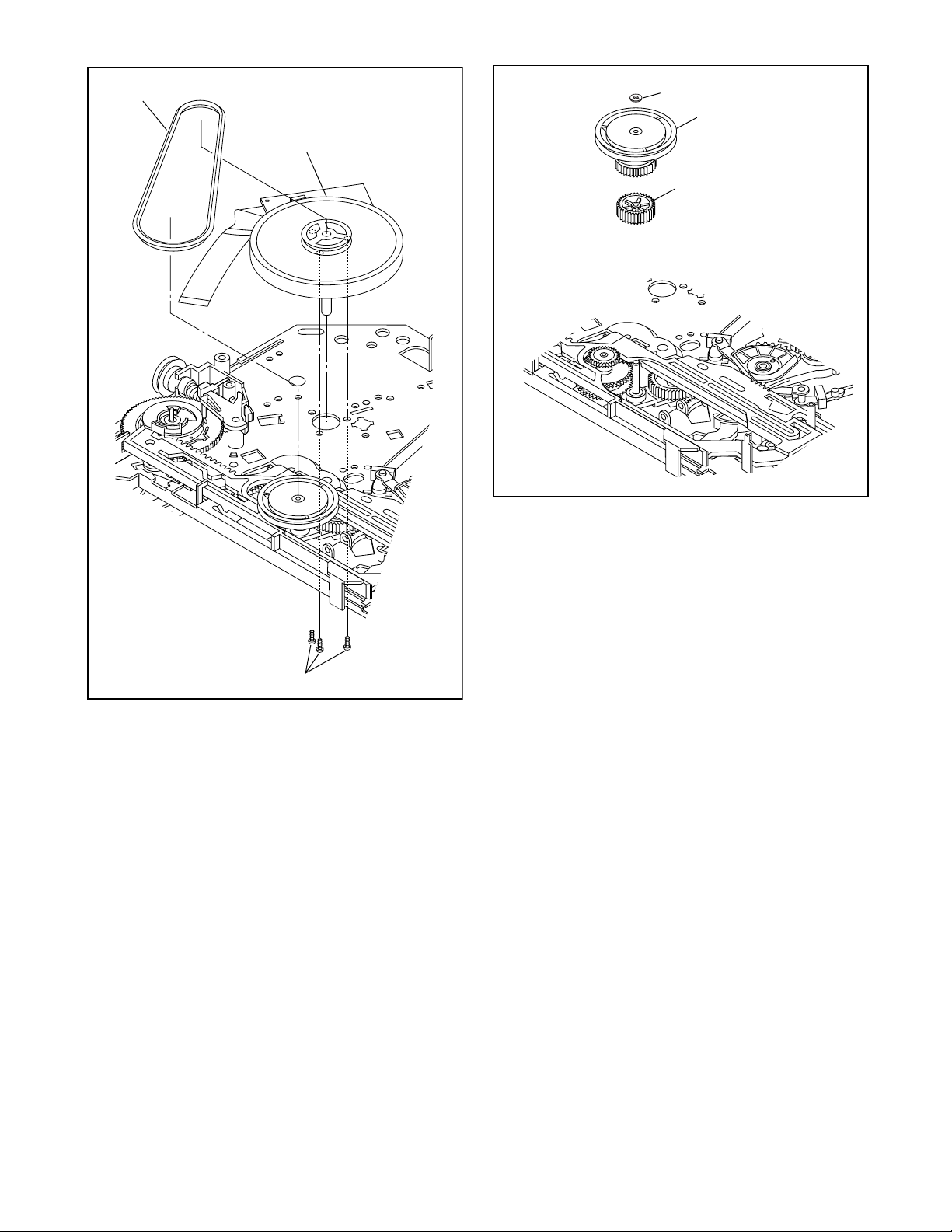
CHAPTER 3 EXPLODED VIEWS AND PARTS LIST
EXPLODED VIEWS
Front Panel
A1X
3-1-1

Cabinet
JACK CBA
2L022
2L022
2L011
A5
2L022
2L022
VT-FX240EUK
only
2B9
2L012
A4
2L011
2B18
2L011
A2
2L041
VT-MX210EUK
only
A4
2L021
2L011
2L021
2L011
2L042
2L021
2L021
2B5
2L051
VT-FX240EUK
only
POWER
SW CBA
2L043
SENSOR CBA
AFV CBA
2L041
2B46
2B7
2B8
2L031
2L021
2L041
2B14
MAIN CBA
2L099
AC001
SENSOR CBA
3-1-2
FUNCTION CBA
A7

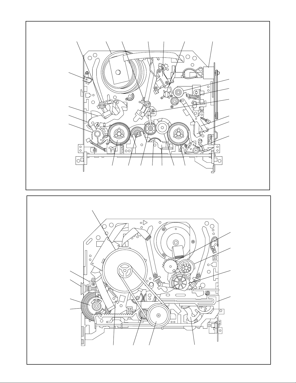
Deck Mechanism View 1
B2
B35
Mark Description
Floil G-374G
SLIDUS OIL #150
(Blue grease)
B9
B73
L1191
B10
L1053
B74
L1051
L1467
B411
B567
B494
B553
B410
Chassis Assembly
Top View (Lubricating Point)
B501
B12
B11
B571
Some Ref. Numbers are not in sequence.
B492
B37
L1450
B426
B121
B560
L1466
B126
L1468
B8
Chassis Assembly
Bottom View (Lubricating Point)
3-1-3

Deck Mechanism View 2
B414
B417
B508
B572
B565
B27
B587
B499
B573
B585
Note: Both the TENSION
LEVER SUB ASSEMBLY
MK11(B27) and the TENSION
LEVER ASSEMBLY MK11
(B587) can be used.
B487
B521
B574
B520
B416
B518
B564
Mark Description
Floil G-374G
SANKOUL FG84M
SLIDUS OIL #150
B148
L1406
B522
B31
B525
(Blue grease)
(Yellow grease)
B3
B558
B557
B579
View
for A
B568
B559
B578
B579
B582
B580
B583
B133
B581
B551
A
B516
B584
B507
B569
B505
B488
B491
B570
B502
B513
Bottom Side (Grease point)
L1151
Bottom Side
(Grease point)
3-1-4
B52
Some Ref. Numbers are not in sequence.

Deck Mechanism View 3
Mark Description
Floil G-374G
(Blue grease)
SLIDUS OIL #150
L1321
B355
L1341
B347
B482
L1321
B354
Note: There are two types (A and B) of B529 (CLEANER
ASSEMBLY), which includes B359 (CLEANER LEVER), B360
(CLEANER ROLLER), B361 (CL POST), etc. These types of
B529 (CLEANER ASSEMBLY) are compatible, and there is no
problem when using either, but it is recommended that you
replace the assembly with the same type if possible.
Refer to Table 1 for details and the combination, (also, refer to
the mechanical parts list on page 3-2-1).
B529 B359 B360 B361
Type
CLEANER
ASSEMBLY
A TJ15103
TJ15746
B
B483
CLEANER
LEVER
TJ15729 Not Used
CLEANER
ROLLER
TJ15104
CL
POST
TJ15105
B529
Type B
B360
B425
L1461
B359
B562
B563
L1341
B300
B313
B529
Type A
B360
B359
B361
B555
Some Ref. Numbers are not in sequence.
B303
B514
3-1-5

REPLACEMENT PARTS LIST
Mechanical Parts List
SYMBOL-NO P-NO DESCRIPTION
MECHANISM SECTION
A1X TS17581 FRONT ASSEMBLY [MX210EUK]
A1X TS17582 FRONT ASSEMBLY [FX240EUK]
A2 TJ16041 CASE, TOP
A4 TS17598 JACK BOARD [MX210EUK]
A4 TS17599 JACK BOARD [FX240EUK]
A5 TE15285 JACK BOARD
A7 TJ16042 PANEL, BOTTOM
2B5 TJ15947 SHEILD, CYLINDER
2B7 TJ17593 SHIELD ASSEMBL Y
2B8 TJ15122 BUSH, LED(F)
2B9 TJ16014 CUSHION
2B14 TJ16043 CUSHION(PCB)
2B46 TJ15314 ROHM HOLDER
AC001 TE15235 AC CORD
!
2L011 TJ16047 SCREW 3X12
2L012 TJ16047 SCREW 3X12
2L021 TJ10119 SCREW M3X10
2L022 TJ10119 SCREW M3X10
2L031 TJ15953 SCREW M3X8
2L041 TJ10177 SCREW 3X8
2L042 TJ10177 SCREW 3X8
2L043 TJ10177 SCREW 3X8
2L051 TJ15955 SCREW M3X5
SYMBOL-NO P-NO DESCRIPTION
B359 TJ15103 CLEANER LEVER
B360 TJ15104 CLEANER ROLLER
B361 TJ15105 CL POST
B410 TS17511 PINCH ARM (A) ASSEMBL Y
B411 TJ15181 PINCH SPRING
B414 TS17512 BRAKE (S) ASSEMBL Y
B416 TS17513 BRAKE (T) ASSEMBL Y
B417 TS17694 TENSION SPRING
B425 TJ15185 LOCK LEVER SPRING
B426 TJ15186 KICK PULLEY
B482 TJ15992 CASSETTE PLATE
B483 TJ15292 LOCK LEVER
B487 TJ15293 BAND BRAKE
B488 TJ16032 MODE LEVER
B491 TJ15994 CAM GEAR (A)
B492 TJ15995 MODE GEAR
B494 TJ15996 DOOR OPENER (B)
B499 TJ15196 LEVER HOLDER (T)
B501 TJ15997 WORM HOLDER
B502 TJ15198 CAM GEAR (B)
B505 TJ15998 WASHER
B507 TJ14034 WASHER
B508 TJ15199 BRAKE SPRING (S)
B513 TJ15201 WASHER
B514 TJ15202 SCREW RACK
2L099 TJ15954 SCREW M3X8
B2 TS17692 CYLINDER ASSEMBL Y [MX210EUK]
B2 TS17693 CYLINDER ASSEMBL Y [FX240EUK]
B3 TS17442 LOADING MOTOR ASSEMBL Y
B8 TS17443 PULLEY ASSEMBL Y
B9 TJ15152 MOVING GUIDE (S)
B10 TJ15153 MOVING GUIDE (T)
B11 TS17444 LOADING ARM (T) ASSEMBL Y
B12 TS17445 LOADING ARM (S) ASSEMBL Y
B27 TS17446 TENSION LEVER SUB ASSEMBL Y
B31 TS17447 AC HEAD
B35 TS17448 TAPE GUIDE
B37 TJ16031 CAPSTAN MOTOR
B52 TJ15161 CAP BELT
B73 TS17449 FE HEAD
B74 TJ15163 PRISM
B121 TJ15982 WORM
B126 TJ15983 PULLEY
B133 TJ15288 IDLER ASSEMBL Y
B148 TE12612 TG CAP
B300 TJ15985 CASSETTE DRIVE LEVER (R)
B303 TJ15986 DOOR OPENER
B347 TJ15987 GUIDE HOLDER (A)
B354 TJ15988 SLIDER (R)
B355 TJ15989 SLIDER (L)
B516 TJ14034 WASHER
B518 TJ15203 WASHER
B520 TJ16033 BRAKE SPRING
B521 TJ15209 SOFT SPRING
B522 TJ15206 TG POST
B525 TJ16001 LDG BELT
B529 TS17455 CLEANER ASSEMBL Y
B551 TJ15301 FF ARM
B553 TJ16003 REV SPRING
B555 TJ17694 RACK ASSEMBL Y
B557 TJ15215 MOTOR PULLEY
B558 TJ16004 LOADING MOTOR
B559 TS17515 CLUTCH ASSEMBL Y
B560 TJ15303 KICK SPRING
B562 TJ15221 CASSETTE DRIVE LEVER (L)
B563 TJ15222 SLIDER SHAFT
B564 TJ16034 GEAR (M)
B565 TJ16005 SENSOR GEAR
B567 TJ15226 PINCH ARM (B)
B568 TJ15304 BT ARM
B569 TJ16006 CAM HOLDER
B570 TJ16035 CAM RACK SPRING
B571 TJ10229 WASHER
B572 TJ15203 WASHER
B573 TJ16007 REEL (S)
3-2-1

SYMBOL-NO P-NO DESCRIPTION
B574 TJ16008 REEL (T)
B578 TJ15306 TR GEAR (A)
B579 TJ15307 TR GEAR (B)
B580 TJ16036 TR GEAR (C)
B581 TJ16172 CENTER GEAR
B582 TJ15311 TR GEAR SPRING
B583 TJ14034 WASHER
B584 TJ15312 TR GEAR SHAFT
B585 TJ16009 WASHER
B587 TS17514 TENSION LEVER ASSEMBL Y
L1051 TJ14055 SCREW M2.6X6
L1053 TJ15313 SCREW M2.6X8
L1151 TJ15236 SCREW M2.6X4
L1321 TJ10176 SCREW M3X6
L1341 TE13298 SCREW M2.6X6
L1406 TJ15238 SCREW
L1450 TE12971 SCREW M2.6X5
L1461 TJ14061 SCREW M2.6X6
L1466 TJ14066 SCREW M2.6X6
L1467 TJ15958 SCREW M2.6X5
L1468 TJ15959 SCREW M1.7X12
SYMBOL-NO P-NO DESCRIPTION
ACCESSORIES
X1 TS17591 REMOTE CONTROL UNIT [MX210EUK]
X1 TS17592 REMOTE CONTROL UNIT [FX240EUK]
X3 TE15231 RF CORD
3-2-2

Electrica Parts List
Note: Although some parts in the schematic diagrams have different names from those in the parts list,
there is no problem in replacing parts.
SYMBOL-NO P-NO DESCRIPTION
RESISTOR
VR501 TA14561 CARBON P.O.T. 100K OHM B
SEMI-CONDUCTORS
D2 TC10112 DIODE 1SS133(T-77) [FX240EUK]
D001 TC10752 DIODE 1N4005
D002 TC10752 DIODE 1N4005
D003 TC10752 DIODE 1N4005
D004 TC10752 DIODE 1N4005
D005 TC12441 DIODE BA159
D006 TC10112 DIODE 1SS133(T-77)
D007 TC10112 DIODE 1SS133(T-77)
D008 TC10112 DIODE 1SS133(T-77)
D009 TC10112 DIODE 1SS133(T-77)
D011 TC10753 DIODE ERA18-04
D012 TJ15128 DIODE FR202
D013 TJ15128 DIODE FR202
D014 TC10877 DIODE SB140 [MX210EUK]
D014 TJ14082 DIODE SB340 [FX240EUK]
D015 TC10604 ZENER DIODE MTZJT-779.1C
D016 TC10753 DIODE ERA18-04 [MX210EUK]
D018 TC10112 DIODE 1SS133(T-77)
D019 TJ13895 ZENER DIODE MTZJT-775.6B
D021 TC10112 DIODE 1SS133(T-77)
SYMBOL-NO P-NO DESCRIPTION
IC451 TC12617 IC LA72646M-A-MPB [FX240EUK]
IC501 TC12619 IC M37762MCA-1C1GP
IC503 TJ15338 IC BR24C02F-W
IC561 TC12618 IC PT6958-FN-TP
! Q001 TC12451 FET FS1KM-18A
Q002 TE13243 TRANSISTOR KTC3199(BL)
Q003 TE13243 TRANSISTOR KTC3199(BL)
Q004 TC10778 TRANSISTOR KTC3199(Y)
Q051 TJ15342 TRANSISTOR KRA104M
Q052 TC12591 TRANSISTOR KRC103M
Q053 TC10778 TRANSISTOR KTC3199(Y) [FX240EUK]
Q054 TE13235 TRANSISTOR KTC3203(Y) [MX210EUK]
Q054 TC12301 TRANSISTOR KTC3205(Y) [FX240EUK]
Q056 TJ13923 TRANSISTOR KRA103M
Q057 TC12581 TRANSISTOR KTA1281(Y)
Q058 TC12591 TRANSISTOR KRC103M
Q101 TC10784 TRANSISTOR KTA1266(GR)
Q102 TC10784 TRANSISTOR KTA1266(GR)
Q151 TC10778 TRANSISTOR KTC3199(Y) [MX210EUK]
Q152 TC10778 TRANSISTOR KTC3199(Y) [MX210EUK]
Q351 TC10784 TRANSISTOR KTA1266(GR)
Q352 TC10778 TRANSISTOR KTC3199(Y)
Q401 TC10784 TRANSISTOR KTA1266(GR)
Q402 TE13235 TRANSISTOR KTC3203(Y)
Q403 TJ13923 TRANSISTOR KRA103M
D023 TC12611 ZENER DIODE DZ-5.1BSBT265 [MX210EUK]
D051 TC10752 DIODE 1N4005
D052 TC10112 DIODE 1SS133(T-77)
D053 TC10752 DIODE 1N4005 [MX210EUK]
D053 TC12612 DIODE RL201 B-222-2 [FX240EUK]
D056 TJ13896 ZENER DIODE MTZJT-775.1C
D057 TA14581 CARBON RES. 3.3KOHM1/4W [MX210EUK]
D057 TJ13919 ZENER DIODE MTZJT-7710B [FX240EUK]
D101 TC12613 ZENER DIODE DZ-11BSAT265
D102 TC12613 ZENER DIODE DZ-11BSAT265
D103 TC12613 ZENER DIODE DZ-11BSAT265
D105 TC12613 ZENER DIODE DZ-11BSAT265
D153 TC12613 ZENER DIODE DZ-11BSAT265
D154 TC12613 ZENER DIODE DZ-11BSAT265 [FX240EUK]
D155 TC12613 ZENER DIODE DZ-11BSAT265
D156 TC12613 ZENER DIODE DZ-11BSAT265 [FX240EUK]
D301 TC10112 DIODE 1SS133(T-77)
D501 TC10112 DIODE 1SS133(T-77)
D502 TJ13898 LED SIR-563ST3F P
D553 TC10112 DIODE 1SS133(T-77)
D701 TC10607 ZENER DIODE MTZJT-7733D
IC1 TC12622 IC MSP3417G-QG-B8 [FX240EUK]
! IC001 TE13224 PHOTOCOUPLER LTV-817B-F
IC151 TC12615 IC TC4052BF(EL) [MX210EUK]
IC301 TC12616 IC LA71750AM-MTB
Q404 TC10778 TRANSISTOR KTC3199(Y)
Q405 TC10778 TRANSISTOR KTC3199(Y)
Q406 TC10778 TRANSISTOR KTC3199(Y)
Q451 TC12591 TRANSISTOR KRC103M [FX240EUK]
Q501 TE13243 TRANSISTOR KTC3199(BL)
Q502 TC12591 TRANSISTOR KRC103M
Q503 TJ15141 PHOTO TRANSISTOR PT204-6B-12
Q504 TJ15141 PHOTO TRANSISTOR PT204-6B-12
Q505 TJ15141 PHOTO TRANSISTOR PT204-6B-12
Q551 TE13243 TRANSISTOR KTC3199(BL)
Q552 TC12591 TRANSISTOR KRC103M
PS503 TJ15282 PHOTO INTERRUPTER RPI-302C70
TRANSFORMER
! T001 TA14582 PULSE TRANS
COILS
L1 5121287 INDUCTOR 10UH [FX240EUK]
L3 TJ15421 INDUCTOR 18UH [FX240EUK]
L4 5121287 INDUCTOR 10UH [FX240EUK]
L001 TA12047 BEAD CORE
L002 TA12047 BEAD CORE
! L003 TJ14696 LINE FILTER 50MH
L009 TJ13909 CHOKE COIL 47UH
L010 TJ13909 CHOKE COIL 47UH
L012 TA12561 INDUCTOR 100UH
3-2-3

SYMBOL-NO P-NO DESCRIPTION
L101 TA12047 BEAD CORE
L121 TA12047 BEAD CORE+
L251 TJ15419 INDUCTOR
L301 TA12574 INDUCTOR 56UH
L401 TJ13909 CHOKE COIL 47UH
L402 TJ13909 CHOKE COIL 47UH
L451 TA12561 INDUCTOR 100UH [FX240EUK]
L452 5121289 INDUCTOR 22UH [FX240EUK]
L501 TA12561 INDUCTOR 100UH
L561 TA12561 INDUCTOR 100UH
L701 5121287 INDUCTOR 10UH
L702 TJ13909 CHOKE COIL 47UH
L704 TA12556 INDUCTOR 15UH
L851 TJ15138 INDUCTOR 1.8UH
CRYSTALS
X1 TC12623 X'TAL 18.432MHZ [FX240EUK]
X301 TJ14708 X'TAL 4.433619MHZ
X501 TE15284 X'TAL 12.000MHZ
X502 TJ15146 X'TAL 32.768KHZ(20PPM)
MISCELLANEOUS
SYMBOL-NO P-NO DESCRIPTION
TU701 TE15282 TUNER UNIT TMDG1-635A [MX210EUK]
TU701 TE15283 TUNER UNIT TMDG2-632A [FX240EUK]
CN1 TE15287 ANGLE PIN HEADER(9P)
CN506 TS17596 FNT PCB ASSEMBLY
CN651 TJ15147 ANGLE PIN HEADER(3P)
CN701 TS17597 AFV PCB ASSEMBLY [FX240EUK]
F001 TJ14705 FUSE T1.6AL/250V
!
FH001 TE11084 FUSE HOLDER
FH002 TE11084 FUSE HOLDER
FP562 TC12614 LED DISPLAY LFU-4421-2001A
J902 TA12575 BEAD CORE
JK101 TE15286 RGB CONNECTOR
JK102 TE15286 RGB CONNECTOR
JK751 TE15281 RCA JACK [FX240EUK]
JW001 TE15236 FLAT CABLE(8P) [MX210EUK]
JW001 TE15237 FLAT CABLE(11P) [FX240EUK]
JW002 TE15236 FLAT CABLE(8P) [MX210EUK]
JW002 TE15238 FLAT CABLE(12P) [FX240EUK]
JW003 TE15239 FLAT CABLE(2P)
RS501 TS17691 REMOTE RECEIVER MIM-93M9DKF
SW504 TE11957 TACT SWITCH
SW505 TE11957 TACT SWITCH
SW506 TE15141 LEAF SWITCH
SW507 TJ15142 ROTARY MODE SWITCH
SW510 TE11957 TACT SWITCH
SW657 TE11957 TACT SWITCH
SW661 TE11957 TACT SWITCH
SW662 TE11957 TACT SWITCH
SW663 TE11957 TACT SWITCH
SW664 TE11957 TACT SWITCH
SW665 TE11957 TACT SWITCH
SW666 TE11957 TACT SWITCH
3-2-4

CHAPTER 4
SCHEMATIC AND BLOCK DIAGRAMS/CBA’S
SCHEMATIC DIAGRAMS / CBA’S AND TEST POINTS
Standard Notes
WARNING
Many electrical and mechanical parts in this chassis
have special characteristics. These characteristics
often pass unnoticed and the protection afforded by
them cannot necessarily be obtained by using replacement components rated for higher voltage, wattage,
etc. Replacement parts that have these special safety
characteristics are identified in this manual and its
supplements; electrical components having such features are identified by the mark " ! " in the schematic
diagram and the parts list. Before replacing any of
these components, read the parts list in this manual
carefully. The use of substitute replacement parts that
do not have the same safety characteristics as specified in the parts list may create shock, fire, or other
hazards.
Capacitor Temperature Markings
Mark
(B)
Capacity
change rate
10%
±
Standard
temperature
20°C -25~+85°C
Temperature
range
Notes:
1. Do not use the part number shown on these drawings for ordering. The correct part number is shown
in the parts list, and may be slightly different or
amended since these drawings were prepared.
2. All resistance values are indicated in ohms
3
(K=10
3. Resistor wattages are 1/4W or 1/6W unless otherwise specified.
4. All capacitance values are indicated in µF
(P=10
5. All voltages are DC voltages unless otherwise
specified.
6. Electrical parts such as capacitors, connectors,
diodes, IC’s, transistors, resistors, switches, and
fuses are identified by four digits. The first two digits are not shown for each component. In each
block of the diagram, there is a note such as shown
below to indicate these abbreviated two digits.
, M=106).
-6
µF).
(F) +30 - 80% 20°C -25~+85°C
(SR)
(Z) +30 - 80% 20°C -10~+70°C
Capacitors and transistors are represented by the following symbols.
±
15%
20°C -25~+85°C
CBA Symbols
(Top View) (Bottom View)
+
Electrolytic Capacitor
(Bottom View)
Transistor or Digital Transistor
E C B
(Top View)
NPN Transistor
E C B
(Top View)
PNP Transistor
E C B
Schematic Diagram Symbols
Digital Transistor
(Top View)
E C B
NPN Digital Transistor
(Top View)
PNP Digital
Transistor
E C B
4-1-1

LIST OF CAUTION, NOTES, AND SYMBOLS USED IN THE SCHEMATIC DIAGRAMS ON THE FOLLOWING PAGES:
1. CAUTION:
FOR CONTINUED PROTECTION AGAINST FIRE HAZARD, REPLACE ONLY WITH THE SAME TYPE FUSE.
2. CAUTION:
Fixed Voltage (or Auto voltage selectable) power supply circuit is used in this unit.
If Main Fuse (F001) is blown, first check to see that all components in the power supply circuit are not defective
before you connect the AC plug to the AC power supply. Otherwise it may cause some components in the
power supply circuit to fail.
3. Note:
(1) Do not use the part number shown on the drawings for ordering. The correct part number is shown in the parts
list, and may be slightly different or amended since the drawings were prepared.
(2) To maintain original function and reliability of repaired units, use only original replacement parts which are
listed with their part numbers in the parts list section of the service manual.
4. Wire Connectors
(1) Prefix symbol "CN" means "connector" (can disconnect and reconnect).
(2) Prefix symbol "CL" means "wire-solder holes of the PCB" (wire is soldered directly).
5. Mode: SP/REC
6. Voltage indications for PLAY and REC modes on the schematics are as shown below:
The same voltage for
both PLAY & REC modes
7. How to read converged lines
1-D3
Distinction Area
Line Number
(1 to 3 digits)
Examples:
1. "1-D3" means that line number "1" goes to area "D3".
2. "1-B1" means that line number "1" goes to area "B1".
8. Test Point Information
: Indicates a test point with a jumper wire across a hole in the PCB.
: Used to indicate a test point with a component lead on foil side.
Unit: Volts
5.0
231
5.0
PLAY mode
REC mode
(2.5)
Indicates that the voltage
is not consistent here.
3
AREA D3
2
1
ABCD
AREA B1
1-D3
1-B1
4-1-2
: Used to indicate a test point with no test pin.
: Used to indicate a test point with a test pin.

WIRING DIAGRAM
AC CORD
NOTE FOR WIRE CONNECTORS:
1. PREFIX SYMBOL "CN" MEANS CONNECTOR.
(CAN DISCONNECT AND RECONNECT.)
2. PREFIX SYMBOL "CL" MEANS WIRE-SOLDER
HOLES OF THE PCB.
(WIRE IS SOLDERED DIRECTLY.)
(DECK ASSEMBLY)
AC HEAD ASSEMBLY
AUDIO
ERASE HEAD
AUDIO HEAD
CONTROL HEAD
FE HEAD
CYLINDER ASSEMBLY
DRUM
MOTOR
VIDEO
(L) HEAD
VIDEO
(R) HEAD
VIDEO
(R)1 HEAD
VIDEO
(L)1 HEAD
VIDEO
(L)2 HEAD
VIDEO
(R)2 HEAD
Hi-Fi AUDIO
(R) HEAD
Hi-Fi AUDIO
(L) HEAD
FULL
ERASE HEAD
PG
SENSOR
M
MOTOR
CL287
AE-H
AE-H/FE-H
A-COM
A-PB/REC
CTL(+)
CTL(-)
ANT-IN ANT-OUT
VT-FX240EUK
CN701 CN1
SENSOR CBA
SENSOR CBA
CL504
1
2
3
4
5
6
CAPSTAN MOTOR
MLOADING
AE-H
1
AE-H/FE-H2
A-COM3
A-PB/REC4
CTL(+)5
6
CTL(-)
CL501
FE-H2
FE-H GND1
CL502
12 C-F/R
AL+15V/+12V
11
10 AL+12V(1)
9
P-ON+5V
GND8
C-FG
7
C-CONT
6
GND5
D-FG4
LM-FWD/REV
3
D-CONT
2
D-PG1
VT-MX210EUK
CL253
MAIN CBA
1 NU
SIF
2
3 GND
4
TU-AUDIO(R)
TU-AUDIO(L)5
P-ON+5V
6
P-ON+5V
7
IIC BUS-SCL8
IIC BUS-SDA9
CL151
JW002
1 V-OUT1
GND
2
3 V-IN1
4
AL+12V(2)
NU5
A-OUT1(R)
6
JK1-8P-OUT
7
A-IN1(L)8
NU9
A-IN1(R)
10
GND
11
A-OUT1(L)12
CL152 CL102
JW001
1 V-OUT2
GND
2
3 V-IN2
4
NU
GND5
A-OUT2(R)
6
SC2-IN
7
A-IN2(L)8
A-IN2(R)9
GND
10
A-OUT2(L)
11
1
2
3
4
5
6
7
8
9
CL101
1
2
3
4
5
6
7
8
VT-FX240EUK
9
10
11
12
1
2
3
4
5
6
7
8
VT-FX240EUK
9
10
11
AFV CBA
JACK CBA
JK101
1
3
5
7
9
11
13
15
17
19
21
JK102
1
3
5
7
9
11
13
15
17
19
21
2
4
6
8
10
12
14
16
18
20
2
4
6
8
10
12
14
16
18
20
V(L)1
V-COM2
3 V(R)
JW003
1 1
KEY-1
2
GND
CL509CL508
2
POWER SW CBA
CL253
V(R)-11
V-COM2
3 V(L)-1
V(L)-2
4
V-COM5
V(R)-26
Hi-Fi-A(R)7
Hi-Fi-COM8
1
KEY2
2
GND
3 3
KEY1
CN651CL506
1
2
FUNCTION CBA
Hi-Fi-A(L)9
VT-FX240EUK
4-1-3

Main 1/5 Schematic Diagram
4-1-4

Main 2/5 Schematic Diagram
WF1
V-OUT E-E
10usec 50mV x 10
Waveforms
(TP751 of Main CBA)
WF1
UPPER
WF2
LOWER
V-OUT 0.1V x 10
RF-SW 0.5V x 10
50usec
(TP751 of Main CBA)
(TP302 of Main CBA)
WF5
C-PB 10mV x 10
RF-SW 0.5V x 10
5msec
UPPER
LOWER
WF2
(TP302 of Main CBA)
(TP301 of Main CBA)
4-1-5

Main 3/5 Schematic Diagram
4-1-6

Main 4/5 Schematic Diagram
CAUTION !
Fixed voltage ( or Auto voltage selectable ) power supply circuit is used in this unit.
If Main Fuse (F001) is blown, check to see that all components in the power supply
circuit are not defective before you connect the AC plug to the AC power supply.
Otherwise it may cause some components in the power supply circuit to fail.
CAUTION
FOR CONTINUED PROTECTION AGAINST FIRE HAZARD,
REPLACE ONLY WITH THE SAME TYPE FUSE.
NOTE :
The voltage for parts in hot circuit is measured using
hot GND as a common terminal.
4-1-7

Main 5/5 Schematic Diagram ( VT-FX240EUK )
4-1-8

Function Schematic Diagram
4-1-9

AFV Schematic Diagram (VT-FX240EUK )
4-1-10

Jack Schematic Diagram
4-1-11

Main CBA Top View
CAUTION !
Fixed voltage ( or Auto voltage selectable ) power supply circuit is used in this unit.
If Main Fuse (F001) is blown, check to see that all components in the power supply circuit are not
defective before you connect the AC plug to the AC power supply.
Otherwise it may cause some components in the power supply circuit to fail.
BECAUSE A HOT CHASSIS GROUND IS PRESENT IN THE POWER
SUPPLY CIRCUIT , AN ISOLATION TRANSFORMER MUST BE USED.
ALSO , IN ORDER TO HAVE THE ABILITY TO INCREASE THE INPUT
SLOWLY , WHEN TROUBLESHOOTING THIS TYPE POWER SUPPLY
CIRCUIT , A VARIABLE ISOLATION TRANSFORMER IS REQUIRED.
Sensor CBA Top View
NOTE :
The voltage for parts in hot circuit is measured using
hot GND as a common terminal.
CAUTION
FOR CONTINUED PROTECTION AGAINST FIRE HAZARD,
REPLACE ONLY WITH THE SAME TYPE FUSE.
WF1
TP751
V-OUT
TP506
END-S
WF2
TP302
RF-SW
VR501
SW-P
4-1-12
TP502
S-INH
TP303
CTL
WF5
TP301
C-PB

Main CBA Bottom View
CAUTION !
Fixed voltage ( or Auto voltage selectable ) power supply circuit is used in this unit.
If Main Fuse (F001) is blown, check to see that all components in the power supply circuit are not
defective before you connect the AC plug to the AC power supply.
Otherwise it may cause some components in the power supply circuit to fail.
BECAUSE A HOT CHASSIS GROUND IS PRESENT IN THE POWER
SUPPLY CIRCUIT , AN ISOLATION TRANSFORMER MUST BE USED.
ALSO , IN ORDER TO HAVE THE ABILITY TO INCREASE THE INPUT
SLOWLY , WHEN TROUBLESHOOTING THIS TYPE POWER SUPPLY
CIRCUIT , A VARIABLE ISOLATION TRANSFORMER IS REQUIRED.
NOTE :
The voltage for parts in hot circuit is measured using
hot GND as a common terminal.
CAUTION
FOR CONTINUED PROTECTION AGAINST FIRE HAZARD,
REPLACE ONLY WITH THE SAME TYPE FUSE.
4-1-13

Function CBA Top View Function CBA Bottom View
Power SW CBA Top View
Power SW CBA Bottom View
4-1-14

AFV CBA Top View AFV CBA Bottom View
4-1-15

Jack CBA Top View
Jack CBA Bottom View
4-1-16

Servo/System Control Block Diagram
BLOCK DIAGRAMS
SW510 POWER
POWER SW CBA
(DECK ASSEMBLY)
CONTROL
HEAD
AC HEAD ASSEMBLY
Q504
ST-S
SENSOR CBA
Q505
END-S
SENSOR CBA
CYLINDER ASSEMBLY CAPSTAN MOTOR
PG
SENSOR
DRUM
MOTOR
M
LOADING
MOTOR
CL509
CL287
M
1 1KEY-1
5 5CTL(+)
6 6CTL(-)
CL508
CL504
CAPSTAN
MOTOR
MAIN CBA
TP506
END-S
M
SW507
LD-SW
Q503
T-REEL
AL+5V
PS503
S-REEL
VR501
SW-POINT
CL502
12 C-F/R
11
AL+15V/+12V
10 AL+12V(1)
P-ON+5V
9
GND
8
C-FG
7
C-CONT
6
GND
5
D-FG
4
LM-FWD/REV
3
D-CONT
2
D-PG
1
D502
S-LED
TIMER+5V
AL+5V
FROM/TO
POWER
SUPPLY
BLOCK
AL+5V
Q502
Q501
RESET
AL+5V
SW506
REC-SAFETY
AL+15V/+12V
AL+12V(1)
P-ON+5V
C-POW-SW
P-ON-H
P-DOWN-L
RS501
REMOTE
SENSOR
TP501
CTL
IC501
(SERVO/SYSTEM CONTROL)
CTL97
FF/REW-L84
REMOCON-IN
14
LD-SW9
95
CTL(+)
CTL(-)
94
10
ST-S
4
END-S
T-REEL
80
S-REEL79
RESET
34
PG-DELAY
2
REC-SAF-SW
31
C-F/R
78
C-FG
87
C-CONT
76
D-FG
89
LM-FWD/REV
81
D-CONT77
D-PG
90
C-POW-SW
66
P-ON-H
67
P-DOWN-L
86
KEY- 1
KEY- 2
DRV-DATA
DRV-STB
DRV-CLK
AUDIO-SW-1
AUDIO-SW-2 30
A-MUTE-H
Hi-Fi-H-SW
A-MODE
IIC-BUS SDA
IIC-BUS SCL
D-REC-H
RF-SW
C-ROTA
D-V SYNC
V-ENV
C-SYNC
H-A-SW
H-A-COMP
7
8
68
69
70
VT-MX210EUK
29
83
VT-FX240EUK
19
61
72
71
65
18
15
13
6
58
16
17
VT-FX240EUK
TP507
S-INH
KEY
SWITCH
SW505
CH-UP
IC561
(FIP DRIVER)
DRV-DATA
28
DRV-STB
2
DRV-CLK
1
CL506 CN651
1 1KEY-2
FP562
LED CLOCK
23
G1
22
G2
21
G3
20
G4
S1
7
S2
8
S7
13
S8
14
S9
16
S10
17
AUDIO-SW-1
AUDIO-SW-2
IIC-BUS SDA
IIC-BUS SCL
IIC-BUS SDA
IIC-BUS SCL
IIC-BUS SDA
IIC-BUS SCL
FUNCTION CBA
TU701(TUNER UNIT)
SDA
3
SDA
12
SCL
5
SCL
11
IC503 (MEMORY)
SDA
5
SCL
6
A-MUTE-H
Hi-Fi-H-SW
A-MODE
D-REC-H
RF-SW
C-ROTA
D-V SYNC
V-ENV
C-SYNC
H-A-SW
H-A-COMP
KEY SWITCH
TO
AUDIO BLOCK
FROM/TO
Hi-Fi AUDIO
BLOCK
FROM/TO
VIDEO BLOCK
4-2-1

Video Block Diagram ( VT-MX210EUK )
MAIN CBA
52
BUFFER
Q351
TU701
VIDEO
TU-VIDEO
6
24
IC501 (OSD)
OSD
CHARACTER
MIX
IC301
(Y/C SIGNAL PROCESS)
48
50
52
TUNER
IN1
IN2
TO SERVO/SYSTEM
CONTROL BLOCK
50
65
BYPASS
AGC
IIC BUS SDA
IIC BUS SCL
Y. DELAY
LUMINANCE
SIGNAL
PROCESS
69684643
SERIAL
DECORDER
REC-VIDEO SIGNAL PB-VIDEO SIGNAL MODE: SP/REC
7978
CL253
R
P
HEAD
AMP
96
95
93
94
V(L)
V-COM
V(R)
(DECK ASSEMBLY)
CYLINDER ASSEMBLY
1
2
3
VIDEO (L)
HEAD
VIDEO (R)
HEAD
V-OUT1
V-IN1
V-OUT2
V-IN2
JACK CBA
JK101
19
20
JK102
19
20
Q101
BUFFER
Q102
BUFFER
CL101
1
V-OUT1
V-IN1
3 3
CL102
1
V-OUT2
V-IN2 3
3
CL151
1
CL152
1
WF1
TP751
V-OUT
56
61
63
PB/EE
TUNER
IN1
PB/EE
MUTE
MUTE
IN2
CHARA.
INS.
1/2
FBC
PR
AGC VXO
58 59
Y/C
MIX
CCD 1H DELAY
CHROMINANCE
SIGNAL
PROCESS
2928
X301
4.43MHz
Y
+
C
R P R P
21
TP301
C-PB
WF5
REC FM
AGC
D-REC-H
RF-SW/C-ROTA
D-V-SYNC
V-ENV
C-SYNC
80
70
62
84
67
WF2
TP502
RF-SW
D-REC-H
RF-SW
C-ROTA
D-V-SYNC
V-ENV
C-SYNC
TO SERVO/SYSTEM
CONTROL BLOCK
4-2-2

Video Block Diagram ( VT-FX240EUK )
MAIN CBA
52
BUFFER
Q351
IC501 (OSD)
OSD
CHARACTER
MIX
IC301
(Y/C SIGNAL PROCESS)
TO SERVO/SYSTEM
CONTROL BLOCK
50
65
I2C BUS SDA
I2C BUS SCL
REC-VIDEO SIGNAL PB-VIDEO SIGNAL MODE: SP/REC
69684643
7978
V-OUT1
V-IN1
JACK CBA
JK101
19
20
TU701
Q101
BUFFER
VIDEO
TU-VIDEO
CL101
1
V-OUT1
V-IN1
3 3
24
6
CL151
1
WF1
TP751
V-OUT
48
50
52
56
61
63
TUNER
PB/EE
TUNER
IN1
PB/EE
MUTE
IN1
IN2
IN2
MUTE
Y. DELAY
BYPASS
AGC
CHARA.
INS.
1/2
FBC
PR
AGC VXO
LUMINANCE
SIGNAL
PROCESS
Y/C
MIX
SERIAL
DECORDER
CCD 1H DELAY
CHROMINANCE
SIGNAL
PROCESS
R
Y
+
C
R P R P
P
REC FM
AGC
SP
SP
HEAD
AMP
EP
EP
HEAD
AMP
D-REC-H
RF-SW/C-ROTA
D-V-SYNC
H-A-SW
H-A-COMP
V-ENV
C-SYNC
96
95
93
94
90
89
88
87
80
70
62
71
83
84
67
V-COM
V-COM
WF2
TP502
RF-SW
CL253
V(R)-1
V(L)-1
V(L)-2
V(R)-2
D-REC-H
RF-SW
C-ROTA
D-V-SYNC
H-A-SW
H-A-COMP
V-ENV
C-SYNC
(DECK ASSEMBLY)
CYLINDER ASSEMBLY
1
2
3
4
5
6
TO SERVO/SYSTEM
CONTROL BLOCK
VIDEO (R)-1
HEAD
VIDEO (L)-1
HEAD
VIDEO (L)-2
HEAD
VIDEO (R)-2
HEAD
V-OUT2
V-IN2
JK102
19
20
Q102
BUFFER
CL102
1
V-OUT2
V-IN2 3
3
CL152
1
58 59
X301
4.43MHz
2928
21
TP301
C-PB
WF5
4-2-3

Audio Block Diagram ( VT-MX210EUK )
PB-AUDIO SIGNAL REC-AUDIO SIGNAL Mode : SP/REC
MAIN CBA
TU701
JK101
A-IN1(R)
A-IN1(L)
A-OUT1(R)
A-OUT1(L)
A-IN2(R)
A-IN2(L)
A-OUT2(R)
A-OUT2(L)
2
6
1
3
JK102
2
6
1
3
(DECK ASSEMBLY)
ACE HEAD ASSEMBLY
AUDIO
HEAD
AUDIO
ERASE
HEAD
FE HEAD
FULL
ERASE
HEAD
JACK CBA
A-PB/REC 4
A-COM 3
AE-H 1
AE-H/FE-H 2
CL101
CL102
CL287
8
6
8
6
A-IN1
A-OUT1
A-IN2
A-OUT2
CL151
8
6
CL152
8
6
CL504
4 A-PB/REC
3 A-COM
1 AE-H
2 AE-H/FE-H
CL501
2 FE-H
1 FE-H-GND
TU-AUDIO
Q401
Q402
BIAS
OSC
Q404
(PB=ON)
Q405
(PB=ON)
21
+5V
Q406
Q403
13
15
17
5
6
1
2
SWITCHING
D-REC-OFF
+5V
IC301 (AUDIO SIGNAL PROCESS)
TUNER
IN1
IN2
PB-ON
EQ
AMP
SP/LP-ON
7
AUTO
BIAS
3
Q151
BUFFER
Q152
BUFFER
98
100
INV
IC151 (SWITCHING)
3
13
R
ATT
P
REC
AMP
AUDIO HD-SW
CONTROL
16
PB/EE
PB/EE
PB/EE
IN2
TUNER
PB/EE
IN1
IN1
SW
CTL
ALC
DET
ALC
1
5
2
4
12
14
15
11
10
9
LINE
AMP
REC-ON
SERIAL
DECODER
68 69
AUDIO-SW-1
AUDIO-SW-2
MUTE
71
TO SERVO/SYSTEM
CONTROL BLOCK
A-MUTE-H
IIC BUS-SDA
IIC BUS-SCL
12
11
TO SERVO/SYSTEM
CONTROL BLOCK
4-2-4

Audio Block Diagram ( VT-FX240EUK )
PB-AUDIO SIGNAL REC-AUDIO SIGNAL Mode : SP/REC
MAIN CBA
TO Hi-Fi
AUDIO BLOCK
(DECK ASSEMBLY)
ACE HEAD ASSEMBLY
AUDIO
HEAD
AUDIO
ERASE
HEAD
N-A-PB
N-A-REC
CL287
A-PB/REC 4
A-COM 3
AE-H 1
AE-H/FE-H 2
CL504
4 A-PB/REC
3 A-COM
1 AE-H
2 AE-H/FE-H
Q401
Q402
BIAS
OSC
+5V
Q406
IC301
(AUDIO SIGNAL PROCESS) 1513 17
TUNER IN2
INV
R
98
ATT
P
REC
AMP
5
6
1
2
PB-ON
EQ
AMP
SP/LP-ON
AUTO
BIAS
7
3
100
IN1
ALC
DET
ALC
LINE
AMP
REC-ON
MUTE
12
11
FULL
ERASE
HEAD
FE HEAD
CL501
2 FE-H
1 FE-H-GND
Q404 (PB=ON)
Q403
Q405
(PB=ON)
SWITCHING
D-REC-OFF
+5V
AUDIO HD-SW
CONTROL
16
SERIAL
DECODER
68 69
71
A-MUTE-H
IIC BUS-SDA
IIC BUS-SCL
TO SERVO/SYSTEM
CONTROL BLOCK
4-2-5

Hi-Fi Audio Block Diagram ( VT-FX240EUK )
REC-AUDIO SIGNALPB-AUDIO SIGNAL Mode : SP/REC
A-IN1(R)
A-IN1(L)
A-OUT1(R)
A-OUT1(L)
A-IN2(R)
A-IN2(L)
A-OUT2(R)
A-OUT2(L)
22
2
6
1
3
2
6
1
3
TU701
SIF
JK101
JK102
JACK CBA
CL101
10
12
CL102
11
A-IN1(R)
A-IN1(L) 8
8
6
A-OUT1(R)
A-OUT1(L) 12
9
A-IN2(R)
A-IN2(L) 8
8
6
A-OUT2(R)
A-OUT2(L) 11
AUDIO
CL151
10
6
CL152
9
6
IC451 (MTS/ SAP/ Hi-Fi AUDIO PROCESS/ Hi-Fi HEAD AMP)
76
2
75
69
73
51
65
SW
ALC
D.C.
R-CH
INSEL
SW
ALC
D.C.
R-CH
PNR
47
48
P
R
LIM DEV
MAIN CBA
SW
NOISE
COMP
VCO
OUTPUT
SELECT
R-CH BPF
LPF
DO
DET
SERIAL
DATA
DECODER
ENV
DET
ALC
MUTE
38
39
23
80
78
IIC-BUS SDA
IIC-BUS SCL
Q451
A-MODE
TO
SERVO/ SYSTEM
CONTROL BLOCK
2
4-2-6
67
7
11
53
AFV CBA
CN1
2
SIF
2
IF SINAL
PROCESS
TO AUDIO BLOCK
4
TU-AUDIO(R)
TU-AUDIO(L)
5
N-A-REC
N-A-PB
CN701CN1CN701
4
5
6
4
NOR
SW
L-CH
INSEL
13
14
L-CH
PNR
LIM DEV
R
P
SW
NOISE
HOLD
PULSE
NOISE
DET
VCO
COMP
MIX
LPF
L-CH BPF
LIM
COMP
31 30
40
26
R
L
24
27
Hi-Fi-A(R) 7
Hi-Fi-COM 8
Hi-Fi-A(L) 9
Hi-Fi-H-SW
CYLINDER
ASSEMBLY
CL253
Hi-Fi
AUDIO
(R) HEAD
Hi-Fi
AUDIO
(L) HEAD

Power Supply Block Diagram
AC001
NOTE :
The voltage for parts in hot circuit is measured using
hot GND as a common terminal.
HOT CIRCUIT. BE CAREFUL.
F001
T1.6A L 250V
L003
LINE
FILTER
D001 - D004
BRIDGE
RECTIFIER
CAUTION
FOR CONTINUED PROTECTION AGAINST FIRE HAZARD,
REPLACE ONLY WITH THE SAME TYPE T1.6AL/250V FUSE.
T001
Q051
2
4
Q001
12
Q052
13
14
Q058
15
CAUTION !
Fixed voltage (or Auto voltage selectable ) power supply circuit is used in this unit.
If Main Fuse (F001) is blown, check to see that all components in the power supply
circuit are not defective before you connect the AC plug to the AC power supply.
Otherwise it may cause some components in the power supply circuit to fail.
MAIN CBA
VT-FX240EUK
Q053
P-ON+44V
P-ON-H
AL+15V/+12V
AL+9V
AL+12V
Q057
Q054
C-POW-SW
AL+5V
TIMER+5V
P-ON+5V
P-DOWN-L
AL-5V
HOT
Q003
Q002
7
6
IC001
ERROR
VOLTAGE DET
4
Q004
(SHUNT REGULATOR)
16
VT-MX210EUK
11
17
18
Q056
1
23
COLD
REG
4-2-7

SYSTEM CONTROL TIMING CHARTS
VT-MX210EUK
Mode SW : LD-SW
LD-SW Position detection
A/D Input voltage Limit
(Calculated voltage)
3.76V~4.50V
(4.12V)
4.51V~5.00V
(5.00V)
0.00V~0.25V
(0.00V)
1.06V~1.50V
(1.21V)
0.66V~1.05V
(0.91V)
1.99V~2.60V
(2.17V)
1.51V~1.98V
(1.80V)
3.20V~3.75V
(3.40V)
0.26V~0.65V
(0.44V)
4.51V~5.00V
(5.00V)
2.61V~3.19V
(2.97V)
Note :
EJ RS: Loading FWD (LM-FWD/REV “H”)
RS EJ: Loading REV (LM-FWD/REV “L”)
Stop (A) = Loading
Stop (B) = Unloading
Note :
Symbol Loading Status
EJ Eject
CL Eject ~ REW Reel
SB REW Reel ~ Stop(B)
TL Stop(B) ~ Brake Cancel
FB Brake Cancel
SF ~ Stop(A)
AU Stop(A) ~ Play / REC
AL Play / REC ~ Still / Slow
SS Still / Slow ~ Capstan Reversal
GC Capstan Reversal ~ RS (REW Search)
RS RS (REW Search)
Symbol
EJ
CL
SB
TL
FB
SF
AU
AL
SS
GC
RS
Note:
DISPLAY
-OFF
STOP
PLAY RS
FS
STILLPLAY STOPPLAY
POWER
62 D-REC-H
D-PB-L
0.8S
1.5S(2H)
2.5S(4H)0.2S
0.2S
1.0S
1.0S
0.2S 0.8S
67 P-ON
83 A-MUTE-H
0.3S
6 mS 6 mS160 mS80 mS
ON
ROTATION
DRUM
ON
78 C-F/R
0.2S
0.2S
0.2S
SP MODE
>5.0S 5.0S
LP/SLP MODE
0.4S
Fig. 1
C-DRIVE
"Z"
1.2S
0.4S
0.3S
LM-FWD "M"
/REV
0.2S
PIN NO.
EJ
CL/GC
FB
AU AU
AU
SS
GC
AL
9 LD-SW
CLEJ
SB TL SB
TL
SF FB SF SF ALAL
GC
RS AL AU SFAU
SS
EJECT
CASS.LOAD
LD-FWD
0.2S
LD-REV
0.7S
LD-FWD
0.2S
LD-REV
0.2S
LD-FWD
0.5S
LD-REV
STOP(A)
LD-FWD
PLAY
LD-FWD
RS
LD-REV
0.2S
LD-FWD
FS
PLAY
STILL
NOISE
CANCEL
STILL
NOISE
CANCEL
STILL
PLAY
LD-REV
STOP(A)
ST-S,/
END-S
"OFF"
PLAY
REW
FF
PLAY
PAUSE
PAUSE ON
PAUSE
OFF
PAUSE ON
PAUSE
OFF
PLAY
STOP
/EJECT
81
AL
RS
SF
AU
TL
FB
SS
SB
0.3S
1. EJECT (POWER OFF) -> CASSETTE IN (POWER ON) -> STOP(B) -> STOP(A) -> PLAY -> RS -> FS -> PLAY -> STILL -> PLAY -> STOP(A)
4-3-1

1. EJECT (POWER OFF) -> CASSETTE IN (POWER ON) -> STOP(B) -> STOP(A) -> PLAY -> RS -> FS -> PLAY -> STILL -> PLAY -> STOP(A)
PLAY
PAUSE
PIN NO.
9 LD-SW
CL/GC
EJ
AL
RS
SF
AU
TL
FB
SS
SB
ST-S,/
END-S
EJECT
"OFF"
CLEJ
0.2S
LD-FWD
CASS.LOAD
SB TL SB
0.7S
LD-REV
LD-FWD
TL
FB
0.2S
0.2S
LD-REV
SF FB SF SF ALAL
AU AU
LD-FWD
0.5S
LD-REV
STOP(A)
PLAY
LD-FWD
AU
PLAY
PAUSE
PAUSE ON
PAUSE
OFF
NOISE
CANCEL
PAUSE ON
STILL
REW
PLAY
LD-FWD
GC
SS
FF
LD-REV
RS AL AU SFAU
GCSSAL
0.2S
LD-FWDRSFS
STILL
PLAY
NOISE
CANCEL
OFF
STILL
PLAY
STOP
/EJECT
LD-REV
STOP(A)
81
LM-FWD "M"
78 C-F/R
DRUM
ROTATION
67 P-ON
83 A-MUTE-H
62 D-REC-H
VT-MX210EUK
/REV
C-DRIVE
D-PB-L
DISPLAY
"Z"
ON
ON
POWER
-OFF
1.5S(2H)
2.5S(4H)0.2S
0.2S
1.2S
0.2S
0.2S
STOP
0.4S
0.2S
0.3S
0.2S
0.8S
PLAY RS
0.3S
0.3S
>5.0S 5.0S
LP/SLP MODE
SP MODE
6 mS 6 mS160 mS80 mS
1.0S
FS
STILLPLAY STOPPLAY
1.0S
0.2S 0.8S
0.4S
Fig. 1
EJ
CL
SB
TL
FB
SF
AU
AL
Symbol
SYSTEM CONTROL TIMING CHARTS
(3.40V)
(1.80V)
3.20V~3.75V
A/D Input voltage Limit
LD-SW Position detection
Mode SW : LD-SW
(1.21V)
(0.91V)
3.76V~4.50V
(4.12V)
(5.00V)
(0.00V)
1.06V~1.50V
4.51V~5.00V
0.00V~0.25V
0.66V~1.05V
1.99V~2.60V
(2.17V)
1.51V~1.98V
(Calculated voltage)
0.26V~0.65V
SS
RS
GC
(5.00V)
2.61V~3.19V
(2.97V)
EJ Eject
TL Stop(B) ~ Brake Cancel
CL Eject ~ REW Reel
SB REW Reel ~ Stop(B)
FB Brake Cancel
AL Play / REC ~ Still / Slow
SF ~ Stop(A)
AU Stop(A) ~ Play / REC
SS Still / Slow ~ Capstan Reversal
RS RS (REW Search)
GC Capstan Reversal ~ RS (REW Search)
(0.44V)
4.51V~5.00V
Symbol Loading Status
Note:
Note :
EJ RS: Loading FWD (LM-FWD/REV “H”)
RS EJ: Loading REV (LM-FWD/REV “L”)
Stop (A) = Loading
Stop (B) = Unloading
Note :
4-3-1

2. STOP(A) -> FF -> STOP(A) -> REW -> STOP(A) -> REC -> PAUSE -> PAUSE or REC -> STOP(A) -> EJECT
STOP
PIN NO.
9
LD-SW
CL/GC
EJ
AL
RS
SF
AU
TL
FB
SS
SB
81
LM-FWD "M"
/REV
C-DRIVE
78
C-F/R
DRUM
ROTATION
67
P-ON
FF
0.2S
STOP(A)
LD-REV
SF FBTL AL
FB
"Z"
ON
ON
LD-FWD
FB
0.2S
FF
/EJECT
LD-REV
2.0S
0.5S
LD-FWD
SF SF
AU AU
REW
STOP(A)
LD-REV
TL
AU FB FB AU
0.4S
LD-REV
0.2S
0.2S
STOP
LD-FWD
REW
SF SF SF AUAL ALFBSF
/EJECT
LD-REV
2.0S
LD-FWD
0.5S
0.4S
LD-REV
REC
STOP(A)
0.2S
LD-FWD
REC
PAUSE
GC
SS
LD-FWD
2.5S Short REV
STOP
/EJECT
REC or
PAUSE
LD-FWD
REC PAUSE
LD-REV
0.2S
AU AU
GCSSAL
REC
GCRS AL AL SF FB TL SB CL EJRS SS
SS
LD-FWD
LD-FWD
LD-REV
1.5S
0.2S
GC AL AU
0.5S
0.4S
LD-REV
STOP
/EJECT
STOP(A)
LD-REV
0.2S
LD-REV
0.5S
0.1S
0.2S
0.5S
ST-S,/
END-S
CASS. UNLD
4-3-2
"ON"
EJECT
Fig. 2
83
65
A-MUTE-H
D-PB-L
D-REC-H
DISPLAY
STOP
0.1S
STOPFF
REW STOP
REC
1.2S
RECREC PAUSE STOP

VT-FX240EUK
13 RF-SW
F-AD
(Internal Signal)
The first rise of RF-SW after a rise in F-AD signal
5 C-DRIVE
37 PB CTL
10 C-F/R
AT
"L" "L"
"H"
Acceleration Detection (T1)
"Z"
ST
"H"
BL
Stop detection (T2)
Slow Tracking Value
Reversal Limit Value
11 H-A-SW
12 ROTA
4-3-3
STILL FRAME ADVANCE STILL
Fig. 3

13 RF-SW
F-AD
(Internal Signal)
The first rise of RF-SW after a rise in F-AD signal
AT
5 C-DRIVE
37 PB CTL
10 C-F/R
"H"
"L" "L"
Acceleration Detection (T1)
"Z"
ST
"H"
BL
Stop detection (T2)
Slow Tracking Value
Reversal Limit Value
11 H-A-SW
12 ROTA
STILL STILL
FRAME ADVANCE
Fig. 4
4-3-4

1. EJECT (POWER OFF) -> CASSETTE IN (POWER ON) -> STOP(B) -> STOP(A) -> PLAY -> RS -> FS -> PLAY -> STILL -> PLAY -> STOP(A)
PIN NO.
9 LD-SW
CL/GC
EJ
AL
RS
SF
AU
TL
FB
SS
SB
81
LM-FWD "M"
/REV
C-DRIVE
78 C-F/R
DRUM
ROTATION
67 P-ON
83 A-MUTE-H
D-PB-L
"Z"
ON
ON
ST-S,/
END-S
EJECT
0.2S
"OFF"
CASS.LOAD
CLEJ SB TL SB
0.2S
LD-FWD
2.5S
LD-REV
0.7S
0.2S
LD-FWD
1.2S
0.2S
0.2S
PAUSE
PLAY
0.2S
0.2S
LD-FWD
LD-REV
TL
FB
AU AU
0.5S
LD-REV
0.4S
0.2S
STOP(A)
LD-FWD
AU
REW
PLAY
LD-FWD
GC
SS
FF
RS
LD-REV
RS AL AL AL SFSS
AU AUSF FB SF SF ALAL
GCSSAL
0.3S
0.2S
LD-FWD
FS
(SLOW)
PLAY
PLAY
LD-FWD
PLAY
0.2S
LD-REV
STILL(SLOW)
AL AU
Refer to STILL/
SLOW TIMING
LD-FWD
PLAY
0.3S
STOP
/EJECT
LD-REV
0.4S
STOP(A)
Fig. 5
CHART Fig. 3, 4.
0.3S
0.2S
1.0S
0.8S
0.5S
1.2S
0.2S
65 D-REC-H
DISPLAY
POWER
-OFF
STOP
PLAY RS
FS
STILL(SLOW)PLAY STOPPLAY
4-3-5

2. STOP(A) -> FF -> STOP(A) -> REW -> STOP(A) -> REC -> PAUSE -> PAUSE or REC -> STOP(A) -> EJECT
STOP
PIN NO.
9
LD-SW
CL/GC
EJ
AL
RS
SF
AU
TL
FB
SS
SB
81
LM-FWD "M"
/REV
C-DRIVE
78
C-F/R
DRUM
ROTATION
67
P-ON
FF
0.2S
STOP(A)
LD-REV
FF
LD-FWD
SF FBTL AL
FB
FB
0.2S
"Z"
ON
ON
/EJECT
LD-REV
2.0S
0.5S
LD-FWD
SF SF
AU AU
REW
STOP(A)
LD-REV
TL
AU FB FB AU
0.4S
LD-REV
0.2S
0.2S
STOP
LD-FWD
REW
SF SF SF AUAL ALFBSF
/EJECT
LD-REV
2.0S
LD-FWD
0.5S
LD-REV
0.4S
REC
STOP(A)
0.2S
LD-FWD
REC
PAUSE
GC
SS
LD-FWD
STOP
REC or
PAUSE
LD-FWD
REC PAUSE
LD-REV
2.5S Short REV
GCSSAL
0.2S
AU AU
REC
/EJECT
LD-FWD
GCRS AL AL SF FB TL SB CL EJRS SS
SS
LD-FWD
LD-REV
1.5S
0.2S
GC AL AU
0.5S
0.4S
LD-REV
STOP
/EJECT
STOP(A)
LD-REV
0.2S
LD-REV
0.5S
0.1S
0.2S
0.5S
ST-S,/
END-S
CASS. UNLD
4-3-6
"ON"
EJECT
Fig. 6
83
65
A-MUTE-H
D-PB-L
D-REC-H
DISPLAY
STOP
0.1S
STOPFF
REW STOP
REC
1.2S
RECREC PAUSE STOP

IC PIN FUNCTION DESCRIPTIONS
Comparison Chart of Models and Marks
Model Mark
VT-MX210EUK A
VT-FX240EUK B
IC501( SERVO / SYSTEM CONTROL IC )
“H” ≥ 4.5V, “L” ≤ 1.0V
Pin
Mark
No.
1IN
2IN
3IN
4IN
5IN
6IN
7IN
8IN
9IN
10 OUT
11 -
12 -
13 OUT
14 IN
15 OUT
IN/
Signal
OUT
Name
SC2-IN
PGDELAY
POWSAF
END-S
AFC
V-ENV
KEY-1
KEY-2
LD-SW
ST-S
N.U. Not Used
N.U. Not Used
D-VSYNC
REMOC
ON-IN
CROTA
Function
Input Signal
from Pin 8 of
SCART2
Video Head
Switching Pulse
Signal Adjusted
Voltage
P-ON Power
Detection Input
Signal
Tape End
Position
Detect Signal
Automatic
Frequency
Control Signal
Video Envelope
Comparator
Signal
Key Scan Input
Signal 1
Key Scan Input
Signal 2
Deck Mode
Position
Detector Signal
Tape Start
Position
Detector Signal
Dummy V-sync
Output
Remote
Control Sensor
Color Phase
Rotary
Changeover
SIgnal
Active
Level
L/Hi-z
A/D
A/D
A/D
A/D
A/D
A/D
A/D
A/D
A/D
H/Hi-z
L
H/L
Pin
Mark
No.
16
17
18 OUT
19
20 -
21 -
22 -
23 -
24 -
25 -
26 -
27 -
28 -
29
30
-
31 IN
32 -
33 -
34 IN
35 IN
IN/
OUT
A-
BOUT
A-
BIN
A-
BOUT
A-
BOUT
A-
BOUT
N.U. Not Used
H-A-SW
N.U. Not Used
H-ACOMP
RF-SW
N.U. Not Used
HiFi-H-SWHiFi Audio Head
N.U. Not Used
N.U. Not Used
N.U. Not Used
N.U. Not Used
N.U. Not Used
N.U. Not Used
N.U. Not Used
N.U. Not Used
N.U. Not Used
N.U. Not Used
AUDIOSW1
N.U. Not Used
AUDIOSW2
RECSAFSW
N.U. Not Used
N.U. Not Used
RESET
XC-IN Sub Clock
Signal
Name
Function
Video Head
Amp Switching
Pulse
Head Amp
Comparator
Signal
Video Head
Switching Pulse
Switching Pulse
Audio Input/
Output
Switching
Control Signal 1
(Mono)
Audio Input/
Output
Switching
Control Signal 2
(Mono)
Recording
Safety SW
Detect (With
Record tab="L"/
With out Record
tab="H")
System Reset
Signal
(Reset=”L”)
Active
Level
-
H/L
-
H/L
H/L
-
H/L
-
-
-
-
-
-
-
-
-
-
Z/L
-
Z/L
H
-
-
L
-
4-4-1

Pin
No.
Mark
IN/
OUT
36 OUT
37 -
38 IN
39 OUT
40 -
41 -
42 -
43 IN
44 IN
45 OUT
46 -
47 -
48 IN
49 -
50 IN
51 -
52 OUT
53 -
54 -
55 -
56 -
57 -
58 IN
59 OUT
60 -
A-
61
BIN
62 -
63 -
64 -
65 OUT
Signal
Name
XCOUT
Function
Sub Clock
Vcc Vcc
X-IN
X-OUT
Main Clock
Input
Main Clock
Input
Vss Vss(GND)
N.U. Not Used
N.U. Not Used
CLKSEL
OSC
OSC
T
Clock Select
(GND)
Clock Input
IN
for letter size
Clock Output for
OU
letter size
NU Not Used
LP LP
FSC-IN
[4.43MH
z]
OSDV
4.43MHz Clock
Input
ss OSDVss
VIDEO-INVideo Signal
Input
N.U. Not Used
VIDEOOUT
OSDV
HLF
Video Signal
Output
cc OSDVcc
LPF Connected
Terminal (Slicer)
N.U. Not Used
N.U. Not Used
N.U. Not Used
CSYNC
8POUT1
Composite
Synchronized
Pulse
SCART 1 8Pin
Output Control
Signal
N.U. Not Used
N.U. Not Used
AMODE
Hi-Fi Tape
Detection Signal
N.U. Not Used
N.U. Not Used
N.U. Not Used
D-REC-HDelayed Record
Signal
Active
Level
-
-
-
-
-
-
-
L
-
-
-
-
-
-
-
-
-
-
-
-
-
-
PULSE
H/L
-
-
L
-
-
-
L
Pin
No.
Mark
IN/
OUT
66 OUT
67 IN
68 OUT
69 OUT
70 OUT
71 OUT
72
IN/
OUT
73 -
74 -
75 -
76 OUT
77 OUT
78 OUT
79 IN
80 IN
81 OUT
82 -
83 OUT
84 OUT
85 -
86 IN
Signal
Name
CPOWER
-SW
P-ON-H
DRVDATA
DRVSTB
DRVCLK
IIC
BUSSCL
IIC
BUSSDA
Function
Capstan Power
Switching Pulse
Power On
Signal at High
LED Clock
Driver IC
Control Data
LED Clock
Driver IC Chip
Select Signal
LED Clock
Driver IC
Control Clock
IIC BUS Control
Clock
IIC BUS Control
Data
N.U. Not Used
N.U. Not Used
N.U. Not Used
CCONT
DCONT
Capstan Motor
Control Signal
Drum Motor
Control Signal
Capstan Motor
FWD/REV
C-F/R
Control Signal
(FWD=”L”/
REV=”H”)
S-REEL
T-REEL
LMFWD/
REV
Supply Reel
Rotation Signal
Take Up Reel
Rotation Signal
Loading Motor
Control Signal
N.U. Not Used
AMUTEH
FF/
REW-L
Audio Mute
Control
Signal (Mute =
“H”)
CTL Amp Gain
Switching Signal
(FF/REW=”L”)
N.U. Not Used
PDOWNL
Power Voltage
Down Detector
Signal
Active
Level
L/Hi-z
H
H/L
H/L
H/L
H/L
H/L
-
-
-
PWM
PWM
H/L
PULSE
PULSE
H/L/
Hi-z
-
H
L
-
L
4-4-2

Pin
No.
Mark
IN/
OUT
87 IN
88 -
89 IN
90 IN
91 -
92 -
93 -
94 OUT
95 OUT
96 -
97 -
98 -
99 -
100 -
Signal
Name
Function
Capstan Motor
C-FG
Rotation
Detection
Pulse
AMPV
ss AMPVss (GND)
Drum Motor
D-FG
Rotation
Detection Pulse
D-PG
Drum Motor
Pulse Generator
N.U. Not Used
IN
V-Ref for CTL
AMP
AMPVR
EF
CC Terminal
Playback/
CTL (-)
Record Control
Signal (-)
Playback/
CTL (+)
Record Control
Signal (+)
CTL AMP
AMPC
Connected
Terminal
CTLAMP
out
AMPV
To Monitor for
CTL AMP
Output
cc AMPVcc
A/D Converter
AVcc
Power Input/
Standard
Voltage Input
N.U. Not Used
Active
Level
PULSE
-
PULSE
PULSE
-
-
-
H/L
H/L
-
PULSE
-
-
-
Notes:
Abbreviation for Active Level:
PWM -----Pulse Wide Modulation
A/D--------Analog - Digital Converter
4-4-3

LEAD IDENTIFICATIONS
BN1L4M-T
BN1F4M-T
BA1F4M-T
KTA1266(GR)
KTC3199(Y,GR,BL)
2SC2785(J.H.F.K)
KRA103M
KRC103M
2SA1015-GR(TPE2)
KRA104M
2SD1246(S,T)
E C B
BR24C02F-W
AT24C02N-10SC
M24C02-MN6-T
CAT24WC02JI
8
1
5
4
E C B
LTV-817(B.C)-F
A
K
2SC1815-Y(TPE2)
2SC1815-GR(TPE2)
2SC3266-Y (TPE2)
KTA1281(Y)
2SC2120-Y(TPE2)
KTC3203(Y)
2SC1815-BL(TPE2)
2SA1020(Y)
2SB892(S)
KTC3205(Y)
C
E
81
100
PT-6958-FN-TP
28
1
LA71750AM-MTB
QSZAB0RMB120
80
1
15
14
51
50
31
30
FS1KM-18A
FS1KM-14A
G D S
PT204-6B-12
MID-32A22
C
E
TC4052BF(EL)
BU4052BCF-E2
16
1
34
44
9
8
MSP3407G-QG-B8
MSP3417G-QG-B8
33
1
23
11
61
80
22
12
LA72646M-A-MPB
60
1
41
20
Note:
A: Anode
K: Cathode
E: Emitter
C: Collector
B: Base
R: Reference
S: Source
G: Gate
D: Drain
40
21
4-5-1

VT-FX240EUK/VT-MX210EUK
VT-FX240EUK/VT-MX210EUK
VT-FX240EUK
VT-MX210EUK
Digital Media Division, TokaiNo. 5204ETK
 Loading...