

Page 1
SERVICE MANUAL
PA No. 0239
UT42X902 / D8MW
UT42V702 / D8MW
NTSC
ATSC
ready monitor
D8MW
UT42X902 - P#: HL02561 (CLU-4981S)
Chassis
SERVICE MANUAL REVISION HISTORY INFORMATION
DATE REVISION # REASON
Oct. 03, 2008 SM00001 FIRST ISSUE OF MANUAL
UT42V702 - P#: HL02562 (CLU-4982S)
Remote controls:
SPECIFICATIONS AND PARTS ARE SUBJECT TO CHANGE FOR IMPROVEMENT
LCD DISPLAY PANEL
OCTOBER 2008 HIMEX MANUFACTURING DIVISION
Page 2

SERVICE MANUAL
NTSC
ATSC
ready monitor
D8MW
Chassis
PA No. 0239
UT42X902 / D8MW
UT42V702 / D8MW
Remote controls:
UT42X902 - P#: HL02561 (CLU-4981S)
UT42V702 - P#: HL02562 (CLU-4982S)
TO GO TO A CHAPTER, CLICK ON ITS HEADING BELOW
CONTENTS
SAFETY PRECAUTIONS . . . . . . . . . . . . . . . . . . . . . . . . . . . . . . . . . . . . . . . . . . . 2
PRODUCT SAFETY NOTICE . . . . . . . . . . . . . . . . . . . . . . . . . . . . . . . . . . . . . . . . 3
SERVICING PRECAUTIONS . . . . . . . . . . . . . . . . . . . . . . . . . . . . . . . . . . . . . . . . 4
AGENCY REGULATORY INFORMATION . . . . . . . . . . . . . . . . . . . . . . . . . . . . . . . 9
ACKNOWLEDGEMENTS AND TRADEMARKS . . . . . . . . . . . . . . . . . . . . . . . . . . 9
INTRODUCTION . . . . . . . . . . . . . . . . . . . . . . . . . . . . . . . . . . . . . . . . . . . . . . . . . . 10
SPECIFICATIONS . . . . . . . . . . . . . . . . . . . . . . . . . . . . . . . . . . . . . . . . . . . . . . . . . 11
BASIC SETUP & OPERATION . . . . . . . . . . . . . . . . . . . . . . . . . . . . . . . . . . . . . . . 12
ADJUSTMENTS . . . . . . . . . . . . . . . . . . . . . . . . . . . . . . . . . . . . . . . . . . . . . . . . . . . 14
TROUBLESHOOTING FLOWCHARTS . . . . . . . . . . . . . . . . . . . . . . . . . . . . . . . . . 28
BLOCK DIAGRAM . . . . . . . . . . . . . . . . . . . . . . . . . . . . . . . . . . . . . . . . . . . . . . . . . 33
CONNECTIONS DIAGRAM . . . . . . . . . . . . . . . . . . . . . . . . . . . . . . . . . . . . . . . . . . 34
FINAL WIRING DIAGRAMS . . . . . . . . . . . . . . . . . . . . . . . . . . . . . . . . . . . . . . . . . 35
FINAL ASSEMBLY GUIDE . . . . . . . . . . . . . . . . . . . . . . . . . . . . . . . . . . . . . . . . . . . 41
WAVEFORMS . . . . . . . . . . . . . . . . . . . . . . . . . . . . . . . . . . . . . . . . . . . . . . . . . . . . 50
DC VOLTAGES . . . . . . . . . . . . . . . . . . . . . . . . . . . . . . . . . . . . . . . . . . . . . . . . . . . 53
CIRCUIT SCHEMATIC DIAGRAMS . . . . . . . . . . . . . . . . . . . . . . . . . . . . . . . . . . . 54
PRINTED CIRCUIT BOARDS . . . . . . . . . . . . . . . . . . . . . . . . . . . . . . . . . . . . . . . . 82
PARTS LIST . . . . . . . . . . . . . . . . . . . . . . . . . . . . . . . . . . . . . . . . . . . . . . . . . . . . . . 87
MAIN PARTS VIEW . . . . . . . . . . . . . . . . . . . . . . . . . . . . . . . . . . . . . . . . . . . . . . . . 88
CAUTION:
These servicing instructions are for use by qualied service personnel only. To reduce the
risk of electric shock do not perform any servicing other than that contained in the operating
instructions unless you are qualied to do so. Before servicing this chassis, it is important that
the service technician read the “IMPORTANT SAFETY INSTRUCTIONS” in this service manual.
SAFETY NOTICE: USE ISOLATION TRANSFORMER WHEN SERVICING
Components having special safety characteristics are identied by a ! on the schematics and on the
parts list in this service data and its suplements and bulletins. Before servicing the chassis, it is important
that the service technician read and follow the “Important Safety Instructions” in this service manual.
SPECIFICATIONS AND PARTS ARE SUBJECT TO CHANGE FOR IMPROVEMENT
LCD DISPLAY PANEL
OCTOBER 2008 HIMEX MANUFACTURING DIVISION
Page 3
D8MW
SAFETY PRECAUTIONS
NOTICE: Comply with all cautions and safety-related notes
located on or inside the cover case and on the chassis or
LCD module.
WARNING: Since the chassis of this receiver is connected
to one side of the AC power supply during operation,
whenever the receiver is plugged in service should not
be attempted by anyone unfamiliar with the precautions
necessary when working on this type of receiver.
1. When service is required, an isolation transformer
should be inserted between power line and the receiver
before any service is performed on a “HOT” chassis
receiver.
2. When replacing a chassis in the receiver, all the
protective devices must be put back in place, such as
barriers, nonmetallic knobs, insulating cover-shields,
and isolation resistors, capacitors, etc.
3. When service is required, observe the original lead
dress (wiredress).
4. Always use manufacturer’s replacement components.
Critical components as indicated on the circuit diagram
should not be replaced by another manufacturer’s.
Furthermore, where a short circuit has occurred,
replace those components that indicate evidence of
over heating.
5. Before returning a serviced receiver to the customer,
the service technician must thoroughly test the unit to
be certain that it is completely safe to operate without
danger of electrical shock, and be sure that no protective
device built into the receiver by the manufacturer has
become defective, or inadvertently defeated during
servicing.
Therefore, the following checks should be performed
for the continued protection of the customer and service
technician.
Leakage Current Cold Check
With the AC plug removed from the 120V AC 60Hz source,
place a jumper across Line 1 and Line 2 of the three plug
prongs, do not connect with the third prong, which is
physical ground.
Using an insulation tester (DC500V), connect one of its
leads to the AC plug jumper and touch with the other lead
each exposed metal part (antennas, screwheads, metal
overlays, control shafts, etc.), particularly any exposed
metal part having a return path to the chassis should
have a resistor reading over 4MΩ. Any resistance value
below this range indicates an abnormality which requires
corrective action. An exposed metal part not having a
return path to the chassis will indicate an open circuit.
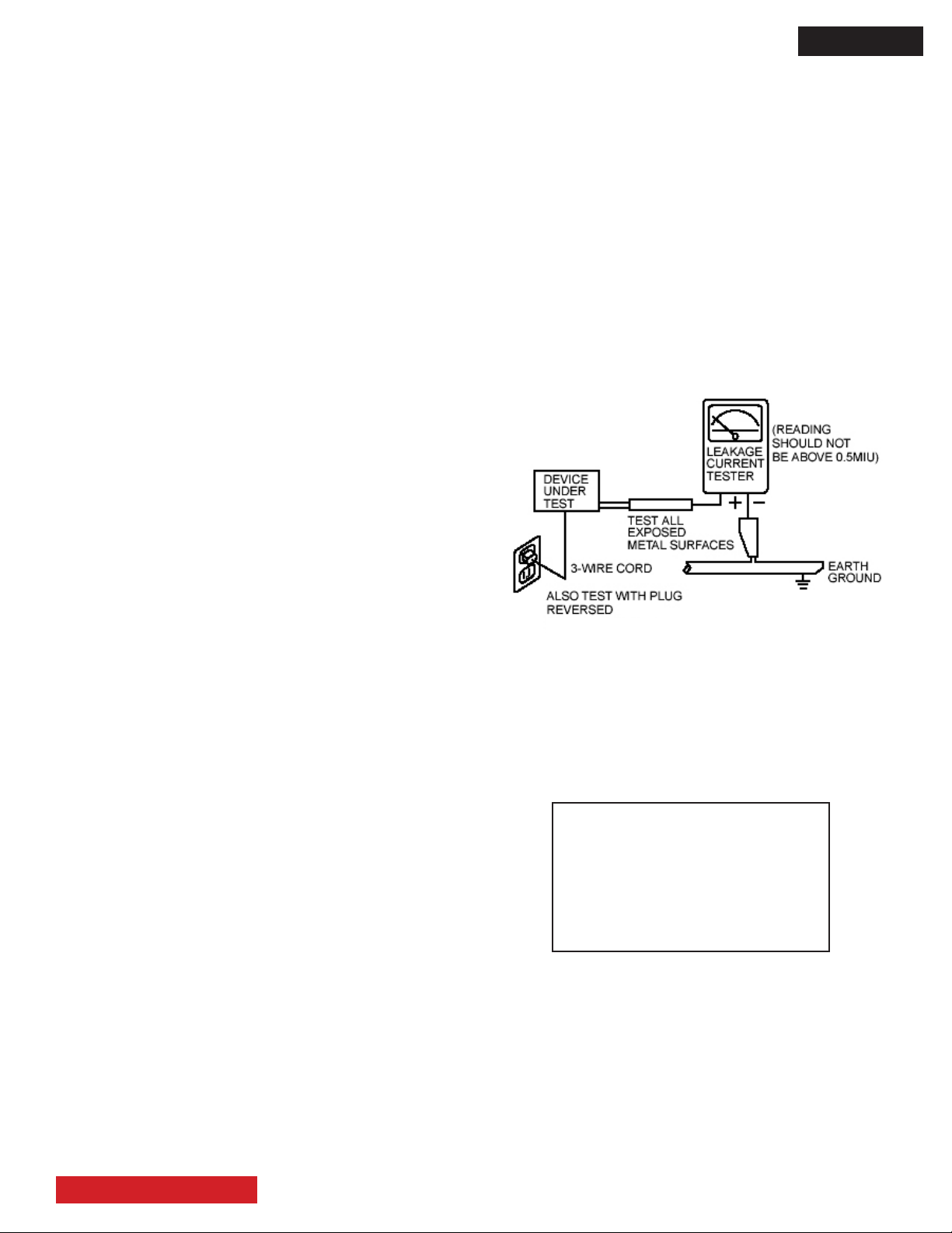
Leakage Current Hot Check
Plug the AC line cord directly into a 120V AC outlet. (Do
not use an isolation transformer during this test.) Use a
leakage current tester or a metering system that complies
with the American National Standards Institute (ANSI)
C101.0 Leakage Current for Appliances. In the case of
the LCD monitor set the AC switch rst in the ON position and then in the OFF position, measure from across
Line 1 and Line 2 of the three plug prongs (do not connect with the third prong which is physical ground), to
all exposed metal parts of the instrument (antennas,
handle bracket, metal cabinet, screw heads, metallic
overlays, control shafts, etc.), especially any exposed
metal parts that offer an electrical return path to the chassis.
Any current measured must not exceed 0.5 MIU. Reverse
the instrument power cord plug in the outlet and repeat test.
AC LEAKAGE TEST
(USING ADAPTER AS
REQUIRED)
ANY MEASUREMENTS NOT WITHIN THE LIMITS
OUTLINED ABOVE ARE INDICATIVE OF A POTENTIAL
SHOCK HAZARD AND MUST BE CORRECTED BEFORE
RETURNING THE RECEIVER TO THE CUSTOMER.
NOTE:
Unplug the AC cord from the power
line before servicing the LCD TV
set.
The Main Power Switch does not
completely cut the AC power.
TABLE OF CONTENTS
2
Page 4

D8MW
PRODUCT SAFETY NOTICE
Many electrical and mechanical parts in HITACHI television
receivers have special safety-related characteristics.
These are often not evident from visual inspection nor can
the protection afforded by them necessarily be obtained
by using replacement components rated for higher
voltage, wattage, etc. Replacement parts which have
these special safety characteristics are identied in this
Service Manual.
Electrical components having such features are identied
with a ! mark in the schematics and parts list in this
Service Manual.
The use of a substitute replacement component which
does not have the same safety characteristics as the
HITACHI recommended replacement component, shown
in the parts list in this Service Manual, may create shock,
re, X-radiation, or other hazards.
Product safety is continuously under review and new
instructions are issued from time to time. For the latest
information, always consult the current HITACHI Service
Manual. A subscription to, or additional copies of HITACHI
Service Manuals may be obtained at a nominal charge
from HITACHI Sales Corporation.
UT42X902 and UT42V702 - LCD monitors
1. Follow the general caution recommendations from
“Safety precautions” section.
2. If necessary to replace Panel module, this work must
be started after the panel module and the AC/DC Power
supply becomes sufciently cool.
3. Special care must be taken with the display area to
avoid damaging its surface.
4. The Panel Module shall not be touched with bare hands
to protect its surface from stains.
5. It is recommended to use clean soft gloves during the
replacing work of the Panel module in order to protect, not
only the display area of the panel module but also the
serviceman.
6. Signal, power supply P.W.B.’s and LCD driving circuits
P.W.B.’s are assembled on the rear side of the LCD
module, take special care with this fragile circuitry.
They are not strong enough to withstand harsh outer
mechanical forces. Extreme bending of the exible
connectors must be avoided too.
SAFETY NOTICE
USE ISOLATION TRANSFORMER
WHEN SERVICING
POWER SOURCE
This LCD television is designed to operate on 120
Volts/60Hz, AC house current. Insert the power cord
into a 120 Volts/60Hz outlet.
NEVER CONNECT THE LCD TV TO OTHER THAN THE
SPECIFIED VOLTAGE OR TO DIRECT CURRENT AND
TO 50HZ. TO PREVENT ELECTRIC SHOCK, DO NOT
USE THE LCD TELEVISION’S (POLARIZED) PLUG
WITH AN EXTENSION CORD, RECEPTACLE, OR THE
OUTLETS UNLESS THE BLADES AND GROUND
TERMINAL CAN BE FULLY INSERTED TO PREVENT
BLADE EXPOSURE.
TABLE OF CONTENTS
3
Page 5

SERVICING PRECAUTIONS
D8MW
CAUTION: Before servicing instruments covered by this
service data and its supplements and addendum, read and
follow the information in previous pages number 2 and 3 of
this publication.
NOTE: If unforeseen circumstances create conict between
the following servicing precautions and any of the safety
precautions on the previous pages of this publication,
always follow the safety precautions. Remember: Safety
First.
General Servicing Guidelines
1. Always unplug the instrument AC power cord from the AC
power source before:
a. Removing or reinstalling any component, circuit board,
module, or any other instrument assembly.
b. Disconnecting or reconnecting any instrument electrical
plug or other electrical connection.
c. Connecting a test substitute in parallel with an electrolytic
capacitor in the instrument.
CAUTION: A wrong part substitution or incorrect polarity
installation of electrolytic capacitors may result in an explosion hazard.
2. Do not spray chemicals on or near this instrument or any
of its assemblies.
3. Unless specied otherwise in these service data, clean
electrical contacts by applying the following mixture to the
contacts with a pipe cleaner, cotton-tipped stick or comparable
nonabrasive applicator: 10% (by volume) Acetone and 90%
(by volume) isopropyl alcohol (90%- 99% strength).
CAUTION: This is a ammable mixture. Unless specied
otherwise in these service data, lubrication of contacts is
not required.
4. Do not defeat any plug/socket of voltage interlocks with
which instruments covered by this service data might be
equipped.
5. Do not apply AC power to this instrument and/or any of its
electrical assemblies unless all solid-state device heatsinks
are correctly installed.
6. Always connect the test instrument ground lead to the
appropriate instrument chassis ground before connecting
the test instrument positive lead. Always remove the test
instrument ground lead last.
7. Use with this instrument only the test xtures specied in
this service data.
Electrostatically Sensitive (ES) Devices
Some semiconductor (solid state) devices can be damaged
easily by static electricity. Such components commonly are
called Electrostatically Sensitive (ES) Devices. Examples
of typical ES devices are integrated circuits and some eld
effect transistors and semiconductor “chip” components.
The following techniques should be used to help reduce
the incidence of component damage caused by static
electricity.
1. Immediately before handling any semiconductor
component or semiconductor-equipped assembly, drain off
any electrostatic charge on your body by touching a known
earth ground. Alternatively, obtain and wear a commercially
available discharging wrist strap device, which should be
removed for potential shock reasons prior to applying power
to the unit under test.
2. After removing an electrical assembly equipped with ES
devices, place the assembly on a conductive surface such
as aluminum foil, to prevent electrostatic charge buildup or
exposure of the assembly.
3. Use only a grounded-tip soldering iron to solder or
desolder ES devices.
4. Use only an anti-static type solder removal device. Some
solder removal devices not classied as “anti-static” can
generate electrical charges sufcient to damage ES
device.
5. Do not use freon-propelled chemicals. These can generate
electrical charges sufcient to damage ES devices.
6. Do not remove a replacement ES device from its protective
package until immediately before you are ready to install it.
(Most replacement ES devices are packaged with leads
electrically shorted together by conductive foam, aluminum
foil or comparable conductive material.)
7. Immediately before removing the protective material from
the leads of a replacement ES device, touch the protective
material to the chassis or circuit assembly into
which the device will be installed.
CAUTION: Be sure no power is applied to the chassis or
circuit, and observe all other safety
precautions.
CAUTION: Do not connect the test xture ground strap
to any heatsink in this instrument.
TABLE OF CONTENTS
8. Minimize bodily motions when handling unpackaged
replacement ES devices. (Otherwise harmless motion
such as the brushing together of your clothes fabric or the
lifting of your foot from a carpeted oor can generate
static electricity sufcient to damage an ES device.)
4
Page 6
D8MW
General Soldering Guidelines
1. Use a grounded-tip, low-wattage soldering iron and
appropriate tip size and shape that will maintain tip
temperature within the range 600°F to 800°F.
2. Use an appropriate lead free solder (see page 8). Lead
solder can be used, but there is a possibility of failure due
to insufcient strength of the solder.
3. Keep the soldering iron tip clean and well-tinned.
4. Thoroughly clean the surfaces to be soldered. Use a
small wire-bristle (0.5 inch or 1.25 cm) brush with a metal
handle. Do not use freon-propelled spray-on cleaners.
5. Use the following desoldering technique.
a. Allow the soldering iron tip to reach normal temperature
(600°F to 800°F).
b. Heat the component lead until the solder melts.
Quickly draw away the melted solder with an antistatic,
suction-type solder removal device or with solder braid.
CAUTION: Work quickly to avoid overheating the circuit
board printed foil.
6. Use the following soldering technique.
a. Allow the soldering iron tip to reach normal temperature
(600°F to 800°F).
b. First, hold the soldering iron tip and solder strand against
the component lead until the solder melts.
c. Quickly move the soldering iron tip to the junction of
the component lead and the printed circuit foil, and hold it
there only until the solder ows onto and around both the
component lead and the foil.
CAUTION: Work quickly to avoid overheating the circuit
board printed foil or components.
d. Closely inspect the solder area and remove any
excess or splashed solder with a small wire-bristle
brush.
Removal
1. Desolder and straighten each IC lead in one operation by
gently prying up on the lead with the soldering iron tip as the
solder melts.
2. Draw away the melted solder with an anti-static suctiontype
solder removal device (or with solder braid) before removing
the IC.
Replacement
1. Carefully insert the replacement IC in the circuit board.
2. Carefully bend each IC lead against the circuit foil pad
and solder it.
3. Clean the soldered areas with a small wire-bristle brush.
(It is not necessary to reapply acrylic coating to areas.)
“Small-signal” Discrete Transistor Removal/
Replacement
1. Remove the defective transistor by clipping its leads as
close as possible to the component body.
2. Bend into a “U” shape the end of each of the three leads
remaining on the circuit board.
3. Bend into a “U” shape the replacement transistor leads.
4. Connect the replacement transistor leads to the
corresponding leads extending from the circuit board and
crimp the “U” with long nose pliers to insure metal to metal
contact, then solder each connection.
Power Output Transistor Devices Removal/
Replacements
1. Heat and remove all solder from around the transistor
leads.
2. Remove the heatsink mounting screw (if so equipped).
3. Carefully remove the transistor from the circuit board.
4. Insert new transistor in circuit board.
5. Solder each transistor lead, and clip off excess lead.
6. Replace heatsink.
Use soldering iron to pry the leads.
IC Removal/Replacement
Some Hitachi unitized chassis circuit boards have slotted
holes (oblong) through which the IC leads are inserted
and then bent at against the circuit foil. When holes are
the slotted type, the following technique should be used
to remove and replace the IC. When working with boards
using the familiar round hole, use the standard technique
as outlined in paragraphs 5 and 6 above.
TABLE OF CONTENTS
Diode Removal/Replacement
1. Remove defective diode by clipping its leads as close as
possible to diode body.
2. Bend the two remaining leads perpendicularly to the circuit
board.
3. Observing diode polarity, wrap each lead of the new diode
around the corresponding lead on the circuit board.
4. Securely crimp each connection and solder it.
5. Inspect (on the circuit board copper side) the solder joints
of the two “original leads”. If they are not shiny, reheat them
and, if necessary, apply additional solder.
5
Page 7
Fuses and Conventional Resistor Removal/
Replacement
1. Clip each fuse or resistor lead at top of circuit board
hollow stake.
2. Securely crimp leads of replacement component around
stake 1/8 inch from top.
3. Solder the connections.
CAUTION: Maintain original spacing between the
replaced component and adjacent components and
the circuit board, to prevent excessive component
temperatures.
Circuit Board Foil Repair
Excessive heat applied to the copper foil of any printed
circuit board will weaken the adhesive that bonds the
foil to the circuit board, causing the foil to separate
from, or “liftoff,” the board. The following guidelines and
procedures should be followed whenever this condition is
encountered.
In Critical Copper Pattern Areas
High component/copper pattern density and/or special
voltage/current characteristics make the spacing and
integrity of copper pattern in some circuit board areas
more critical than in others. The circuit foil in these areas is
designated as Critical Copper Pattern. Because Critical
Copper Pattern requires special soldering techniques to
ensure the maintenance of reliability and safety standards,
contact your Hitachi personnel.
At IC Connections
To repair defective copper pattern at IC connections, use
the following procedure to install a jumper wire on the
copper pattern side of the circuit board. (Use this technique
only on IC connections.)
1. Carefully remove the damaged copper pattern with a
sharp knife. (Remove only as much copper as absolutely
necessary.)
2. Carefully scratch away the solder resist and acrylic
coating (if used) from the end of the remaining copper
pattern.
D8MW
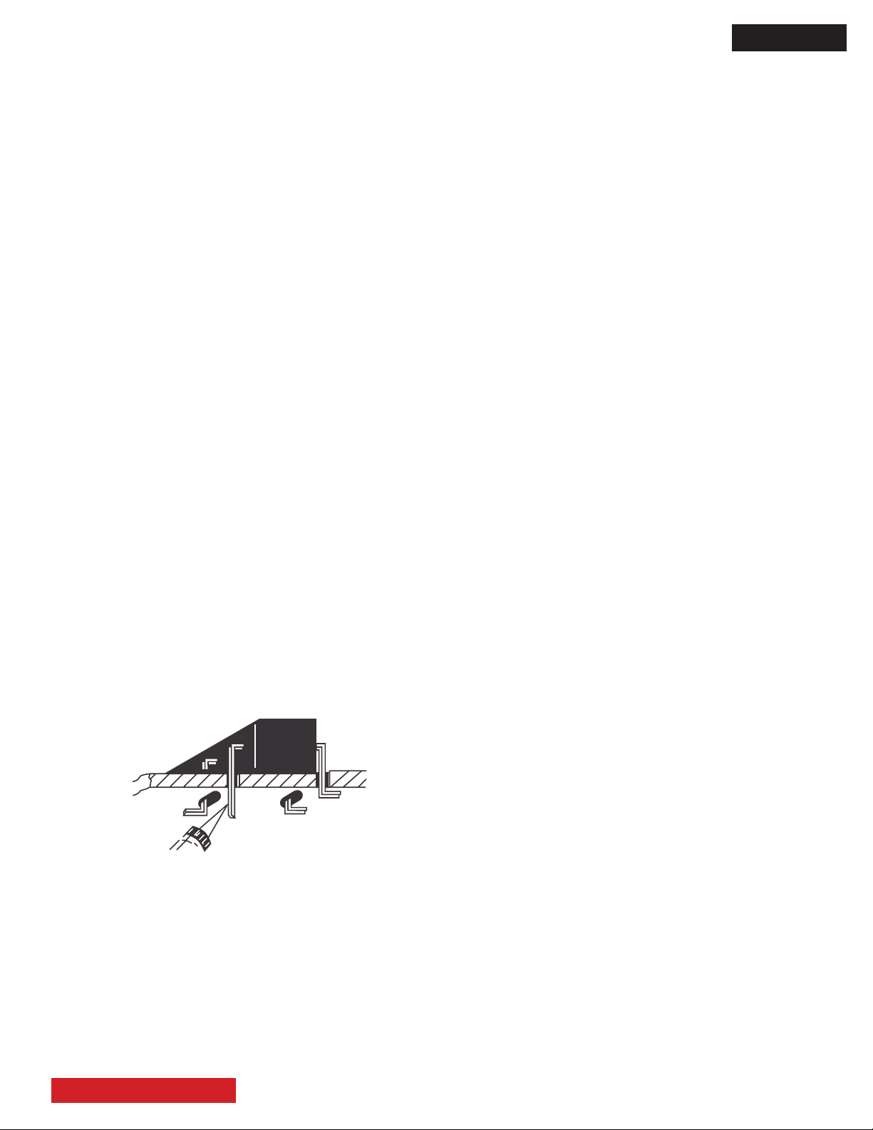
At Other Connections
Use the following technique to repair defective copper
pattern at connections other than IC Pins. This technique
involves the installation of a jumper wire on the component
side of the circuit board.
DEFECTIVE
COPPER
REMOVED
Insulated jumper wire
1. Remove the defective copper pattern with a sharp knife.
Remove at least 1/4 inch of copper, to ensure hazardous
condition will not exist if the jumper wire opens.
2. Trace along the copper pattern from both wire sides of
the pattern break and locate the nearest component directly
connected to the affected copper pattern.
3. Connect insulated 20-gauge jumper wire from the nearest
component on one side of the pattern break to the lead of
the nearest component on the other side.
Carefully crimp and solder the connections.
CAUTION: Be sure the insulated jumper wire is dressed so
that it does not touch components or sharp edges.
BARE JUMPER
WIRE
CRIMP AND
SOLDER
Install jumper wire and solder.
3. Bend a small “U” in one end of a small-gauge jumper
wire and carefully crimp it around the IC pin. Solder the IC
connection.
4. Route the jumper wire along the path of the cut-away
copper pattern and let it overlap the previously scraped
end of the good copper pattern. Solder the overlapped
area, and clip off any excess jumper wire.
TABLE OF CONTENTS
6
Page 8
D8MW
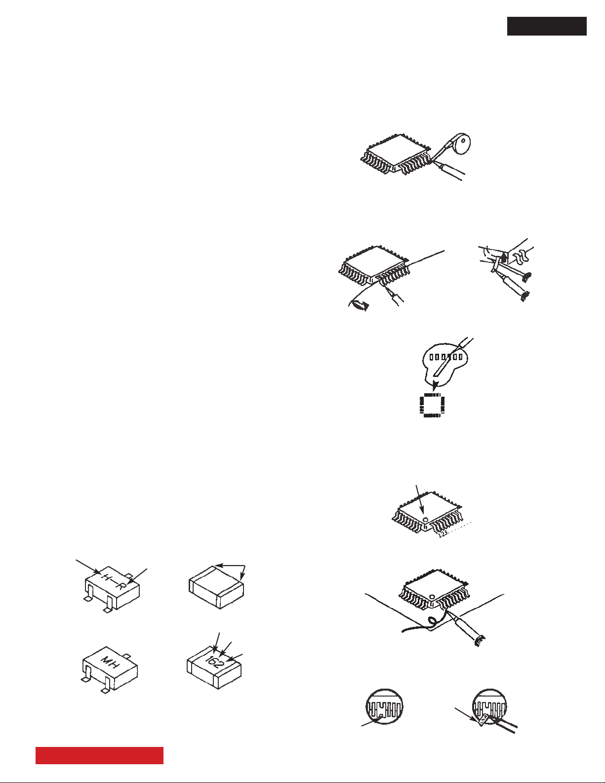
Leadless Chip Components
(surface mount)
Chip components must be replaced with identical chips
due to critical foil track spacing. There are no holes in
the board to mount standard transistors or diodes. Some
chip capacitor or resistor board solder pads may have
holes through the board, however the hole diameter
limits standard resistor replacement to 1/8 watt. Standard
capacitors may also be limited for the same reason. It is
recommended that identical chip components be used.
Chip resistors have a three digit numerical resistance
code -1st and 2nd signicant digits and a multiplier.
Example: 162 = 1600 or 1.6KΩ resistor, 0 = 0Ω
(jumper).
Chip capacitors generally do not have the value indicated
on the capacitor. The color of the component indicates the
general range of the capacitance.
Chip transistors are identied by a two letter code. The
rst letter indicates the type and the second letter, the
grade of transistor.
Chip diodes have a two letter identication code as per the
code chart and are a dual diode pack with either common
anode or common cathode. Check the parts list for correct
diode number.
Component Removal
1. Use solder wick to remove solder from component
end caps or terminals.
2. Without pulling up, carefully twist the component
with tweezers to break the adhesive.
3. Do not reuse removed leadless or chip
components since they are subject to stress
fracture during removal .
Chip Component Installation
1. Put a small amount of solder on the board
soldering pads.
2. Hold the chip component against the soldering
pads with tweezers or with a miniature alligator
clip and apply heat to the pad area with a 30 watt
iron until solder ows. Do not apply heat for more
than 3 seconds
How to Replace Flat-lC
—Required Tools—
• Soldering iron • iron wire or small awl
• De-solder braids • Magnier
1. Remove the solder from all of the pins of a Flat-lC
by using a de-solder braid.
De-Solder
Braid
Soldering
Iron
2. Put the iron wire under the pins of the Flat-lC and pull
it in the direction indicated while heating the pins using a
soldering iron. A small awl can be used instead of the iron
wire.
Pull
Soldering
Iron
Iron
Wire
Awl
Soldering
Iron
3. Remove the solder from all of the pads of the Flat-lC by
using a de-solder braid.
Soldering
Iron
De-Solder
Braid
Flat-IC
4. Position the new Flat-lC in place (apply the pins of the
Flat-lC to the soldering pads where the pins need to be
soldered). Properly determine the positions of the soldering
pads and pins by correctly aligning the polarity symbol.
Polarity Symbol
TYPE
B
E
ANODES
MH DIODE
C
GRADE
TRANSISTOR
COMMON CATHODE
TABLE OF CONTENTS
Chip Components
SOLDER CAPS
1STDIGIT
RESISTOR
SOLDER
CAPS
CAPACITOR
2ND DIGIT
MULTIPLIER
= 1600 = 1.6K
5. Solder all pins to the soldering pads using a ne tipped
soldering iron.
Solder
Soldering
Iron
6. Check with a magnier for solder bridge between the pins
or for dry joint between pins and soldering pads. To remove
a solder bridge, use a de-solder braid as shown in the gure
below.
Bridge
Solder
De-Solder
Braid
Soldering
Iron
7
Page 9
Information for service about the lead-free solder introduction.
Hitachi introduced lead-free solder to conserve the “Earth Environment”.
Please refer to the following before servicing.
(1) Characteristic of lead-free solder
Melting point of lead free solder is 40-50°C higher than solder containing lead.
(2) Solder for service
Following composition is recommended.
“ Sn - 3.0Ag - 0.5Cu “ , or “ Sn - 0.7 Cu “
Lead solder can be used, but there is a possibility of failure due to insufcient strength of the solder.
Caution when using solder containing lead.
Please remove previous solder as much as possible from the soldering point.
When soldering, please perfectly melt the lead-free solder to mix well with the previous solder.
(3) Soldering iron for lead-free solder.
Melting point of lead-free solder is higher than solder containing lead.
Use of a soldering tool “with temperature control” and “with much thermal capacitance” is recommended.
(Recommended temperature control : 320°C - 450°C; [608°F - 842°F])
Recommended temperature
PWB with chip parts 320°C +/- 30°C (608°F +/- 86°F)
PWB without chip parts 380°C +/- 30°C (716°F +/- 86°F)
Chassis, metal, shield etc. 420°C +/- 30°C (788 °F +/- 86°F)
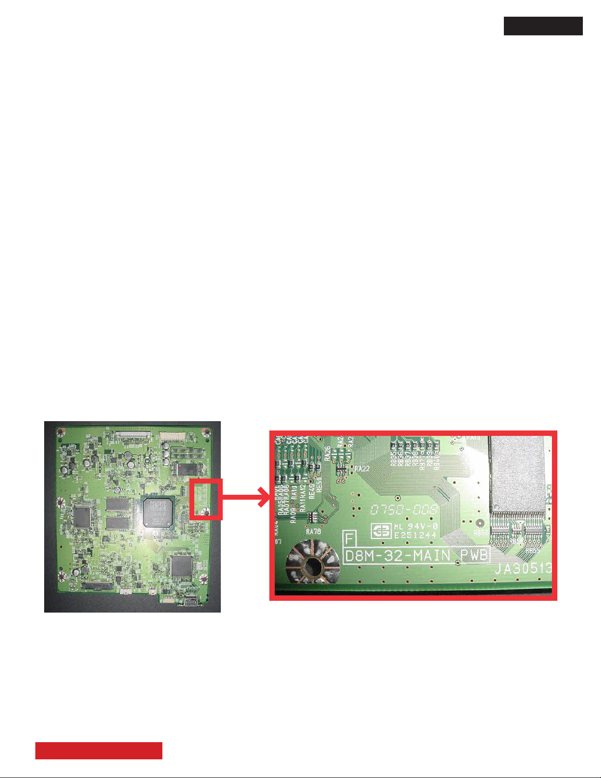
D8MW
(4) Identication of lead-free PWB
2004 models >> lead-free solder is introduced
2006 models >> lead-free solder applied
On lead-free PWB, “F” is added at the beginning of stamp on PWB.
TABLE OF CONTENTS
8
Page 10

AGENCY REGULATORY INFORMATION
Federal Communications Commission Notice
This equipment has been tested and found to comply with the limits for a Class B digital device, pursuant
to Part 15 of the FCC Rules. These limits are designed to provide reasonable protection against harmful
interference in a residential installation. This equipment generates, uses and can radiate radio frequency
energy and if not installed and used in accordance with the instructions, may cause harmful interference
to radio communications. However, there is no guarantee that interference will not occur in a particular installation. If this equipment does cause harmful interference to radio or television reception, which can be
determined by turning the equipment off and on, the user is encouraged to try to correct the interference by
one or more of the following measures:
• Reorient or relocate the receiving antenna.
• Increase the separation between the equipment and the receiver.
• Connect the equipment into an outlet on a circuit different from that to which the receiver is connected.
• Consult the dealer or an experienced radio/television technician for help.
FCC Information
This device complies with part15 of the FCC Rules.Operation is subject to the following two conditions :
(1) This device may not cause harmful interference and (2) This device must accept any interference
received, including interference that may cause undesired operation.
D8MW
Modications
The FCC requires the user to be notied that any changes or modications made to this device that are not
expressly approved by Hitachi Home Electronics (America), Inc. may void the user’s authority to operate
the equipment.
Cables
Connections to this device must be made with shielded cables with metallic RFI/EMI connector hoods to
maintain compliance with FCC Rules and Regulations.
Any cables that are supplied with the system must be replaced with identical cables in order to assure
compliance with FCC rules. Order Hitachi spares as replacement cables.
INDUSTRY CANADA AGENCY REGULATORY INFORMATION
This class B digital apparatus meets all requirements of the Canadian Interference-Causing Equipment
Regulations.
This Class B digital apparatus complies with Canadian ICES-003.
Cet appareil numérique de la classe B est conforme à la norme NMB-003 du Canada.
ACKNOWLEDGMENTS
AND TRADEMARKS
HDMI, the HDMI logo and High-Denition Multimedia Interface are
trademarks or registered trademarks of HDMI Licensing LLC.
• VGA and XGA are trademarks of International Business Machines Corporation.
• VESA is a registered trademark of the Video Electronics Standard Association.
TABLE OF CONTENTS
9
Page 11
D8MW
19-
12/16
(502)
40-
13/16
(1036.2)
36-
3/4
(934)
19-
11/16
(500)
28-
11/16
(728)
26-
11/16
(678)
1-
15/16
(50)
16-
5/16
(413.7)
7-
7/8
(200)
20-
3/4
(526.8)
12-
3/16
(310)
1-
9/16
(39.9) Max5-
3/8
(136)
1-
3/8
(35.0) Min
INTRODUCTION
This HITACHI Service Manual is intended for the qualied service personnel and it contains the necessary infor-
mation for troubleshooting the LCD television set in case of malfunction.
This service manual includes the information for the next models and chassis.
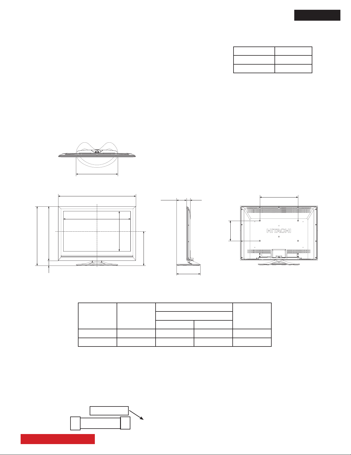
DIMENSIONS:
MODEL CHASSIS
UT42X902 D8MW
UT42V702 D8MW
Height: Excluding stand - 26 11/16”, Including stand - 28 11/16”.
Width: 40 13/16”.
Depth: Excluding stand - 1 9/16”, Including stand - 12 3/16”.
Weigth: Excluding stand - 18.0 kg; Including stand - 20.9 kg.
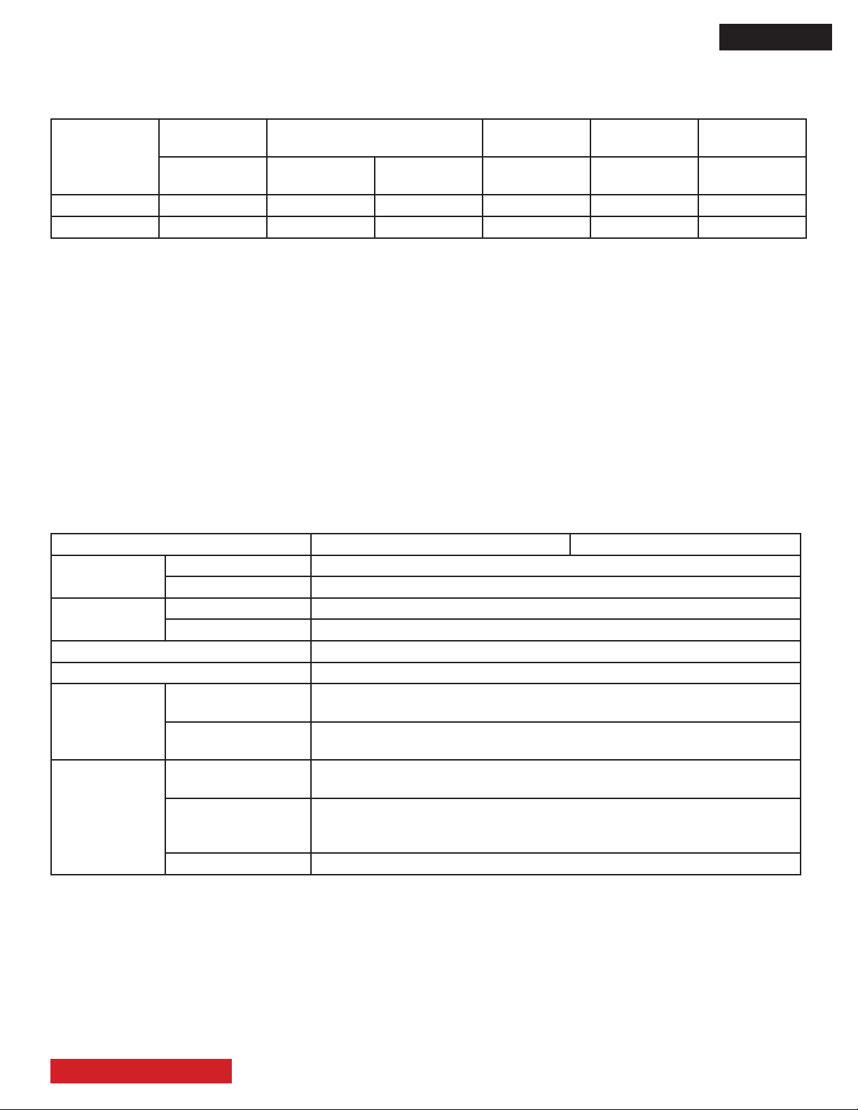
POWER RATINGS:
Indicated Value
No.
Model
Name
ChassisMax Rating
(W) (A)
1 UT42X902 243 2.3 D8MW
CIRCUIT PROTECTION:
2 UT42V702 243 2.3 D8MW
CAUTION: It is very important to replace the fuse with the same kind of fuse as original.
The fuse rating is indicated in the silk of the printed circuit board near the fuse location.
Example: Hitachi part number of the fuse is: FN00562.
High breaking capacity ceramic tube fuse (Time-Lag fuse)
This means the fuse rating is 6.3A, 250V.
TABLE OF CONTENTS
T6.3AH 250V
10
Page 12
TERMINALS AND JACKS
D8MW
HDMI
MODEL
NAME
UT42X902 1 1 1 1 1 1
UT42V702 1 1 1 1 1 1
MAIN FEATURES
• Ultra-slim-line LCD monitor.
• Large-screen and high denition LCD.
• Enjoy high resolution display (1920 (H) x 1080 (V) pixels).
• Improved digital signal processor.
• High quality sound with deeper, richer tones and bass boost.
• Accepts a digital input device with HDMI terminal.
• Enjoy the image from your PC with a large, high-denition LCD screen.
• Easy-to-use On-screen Display system operated by remote control.
• Low power consumption with power saving feature.
SPECIFICATIONS
TERMINAL
HDMI
D-SUB 15 PIN
ANALOG
RGB
COMPOSITE
VIDEO
3.5 MINI
JACK
ANALOG
AUDIO
8 PIN
MINI-DIN
RS-232C
3.5 STEREO
MINI JACK
IR-
THROUGH
SPECIFICATION UT42X902 UT42V702
Panel
Ambient
conditions
Power supply AC120V, 60Hz
Audio output speaker 6W + 6W
HDMI input
RGB/Composite
input
* This analog audio input terminal can be used for PC (RGB) or HDMI-DVI.
Display dimensions Approx. 42 inches measured diagonal (36 3/4 (H) x 20 3/4 (V) in.
Resolution 1920 (H) x 1080 (V) pixels
Temperature Operating: 5ºC to 35ºC, Storage: 0ºC to 40ºC
Relative humidity Operating: 20% to 80%, Storage: 20% to 90% (non-condensing)
Input terminals
Input signals
Input terminals
Input signals
Sync signals H/V separate, TTL level [2KW]
HDMI: HDMI input terminal
Audio input terminal (Mini-pin)*
HDMI: VGA/60, 480i, 576i, 480p, 576p, 720p/50, 720p/60, 1080i/50,
1080i/60, 1080p/50, /1080p/60, 1080p/24.
Analog RGB input terminal (D-sub 15 pin)
Audio input terminal (Mini-pin)*
0.7 Vp-p, analog RGB (Recommended Signal)
Composite video: NTSC3.58, NTSC4.43, PAL, SECAM, PAL60, PAL-M,
PAL-N.
TABLE OF CONTENTS
11
Page 13
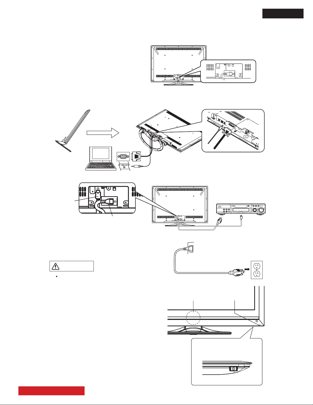
BASIC SETUP AND OPERATION
For more information on connecting and using the monitor, refer to the owner’s guide.
. Connect the power cord to the rear panel.
3 Connect to external equipment.
Example 1: Connecting to PC
To insert D-sub 15 pin, tilt the monitor forward and bring the terminals into view. Two people are required
to hold the monitor and insert D-sub 15 pin safely. Be careful not to damage the panel.
*D-sub 15 and Audio cables are not included.
Example 2: Connecting to DVD player
*
*
Audio Cable
D-Sub 15
Tilt Forward
HDMI Cable
Power Cord
HDMI Cable
Power On...
. Connect the plug into the wall socket after all other
connections are completed.
CAUTION
Ensure that both ends of the power cord are easily
accessible.
The Main Power Switch is factory set to On
(activated), therefore after you connect the plug into
the wall socket, the color of the indicating lamp must
turn Green and the Illumination Lamp turns Blue.The
image will display on screen.
Once the Main Power switch is on, you can turn On/
Off by pressing the Power (On/Off) button on the
remote control.
If no equipment is connected to the Monitor the color
of the indicating lamp turns to Orange, and the
Illumination Lamp turns off indicating Power Save
Mode.
AC
Wall
Socket
Monitor
Rear
Panel
Main Power Switch
(on the underside)
Front
Rear
Illumination Lamp
Indicating Lamp
D8MW
TABLE OF CONTENTS
12
Page 14
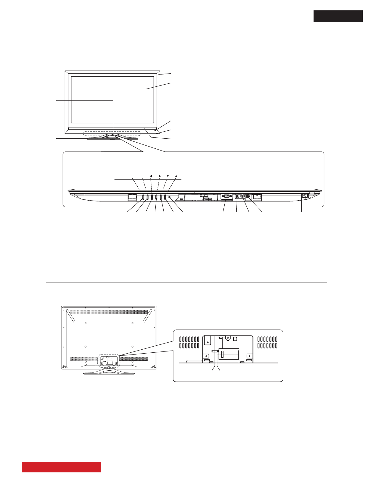
BASIC SETUP AND OPERATION
Front Panel
Rear Panel
.
Cabinet
3
Panel
$
Remote Control Receiver
/
Indicating Lamp
1
Speaker
4
Illumination Lamp
2
Desktop Stand
&
Ÿ button
'
ź button
)
Volume Up/Ź button
*
Volume Down/Ż button
+
Input Select/OK button
Menu/Exit button
.
Power Cord Socket
3
HDMI Input Terminal
Please refer to the owner’s guide for detailed information regarding the connections.
.
3
$
/
1
4
2
(
Main Power switch
,
Service use only
"
RS232C
0
PC (RGB)/DVI Analog Audio Input Terminal
#
PC Connection Terminal (D-sub 15 Pin)
%
Reset button.
(,"0#
')*&+
Control panel (located on the bottom)
MENU/EXIT VOLINPUT/OK
%
3 .
D8MW
TABLE OF CONTENTS
13
Page 15

ADJUSTMENTS
TO GO TO A SECTION, CLICK ON ITS HEADING BELOW.
TABLE OF CONTENTS OF ADJUSTMENTS
1. Adjustment procedure start-up
1.1 How to get to the service mode menu . . . . . . . . . . . . . . . . . . . . . . . . . . . . . . . . . . . . . . . . . . 15
1.2 Changing data and selecting adjustment codes . . . . . . . . . . . . . . . . . . . . . . . . . . . . . . . . . . . 15
2. Memory Initialize
2.1 EEPROM All Initialize operation . . . . . . . . . . . . . . . . . . . . . . . . . . . . . . . . . . . . . . . . . . . . . . 16
2.2 EEPROM renew procedure . . . . . . . . . . . . . . . . . . . . . . . . . . . . . . . . . . . . . . . . . . . . . . . . . . 16
2.3 Memory Initialize affected adjustments . . . . . . . . . . . . . . . . . . . . . . . . . . . . . . . . . . . . . . . . . 16
3. Video Adjustment
3.1 RGB amplitude adjustment (PC D-SUB input) . . . . . . . . . . . . . . . . . . . . . . . . . . . . . . . . . . . . 16
3.2 NTSC Composite video adjustment . . . . . . . . . . . . . . . . . . . . . . . . . . . . . . . . . . . . . . . . . . . . 17
4. Video Color Temperature adjustment
4.1 Video Color Temperature adjustment (Cool) . . . . . . . . . . . . . . . . . . . . . . . . . . . . . . . . . . . . . 17
4.2 Video Color Temperature adjustment (Normal) . . . . . . . . . . . . . . . . . . . . . . . . . . . . . . . . . . . 18
4.3 Video Color Temperature adjustment (Warm) . . . . . . . . . . . . . . . . . . . . . . . . . . . . . . . . . . . . 19
5. Another procedure to set to factory shipping conditions . . . . . . . . . . . . . . . . . . . . . . . . . . . . . . . 19
5.1 Factory Shipping Conditions table 20
6. Software upgrade procedure . . . . . . . . . . . . . . . . . . . . . . . . . . . . . . . . . . . . . . . . . . . . . . . . . . . . 22
D8MW
TABLE OF CONTENTS
14
Page 16
D8MW
1. ADJUSTMENT PROCEDURE START-UP
The UT42X902 and the UT42V702 LCD Monitors run through
a series of adjustments at the factory.
After servicing, these adjustments must be done again.
NOTE: - S/W version check -
The software version of the LCD monitor can be checked
under the SETUP OSD menu. The next image shows the
OSD where the version number is shown.
Main
S/W
Till this day, the latest software versions are:
Model Main S/W Sub S/W
All UT42” VS224 223
Sub
S/W
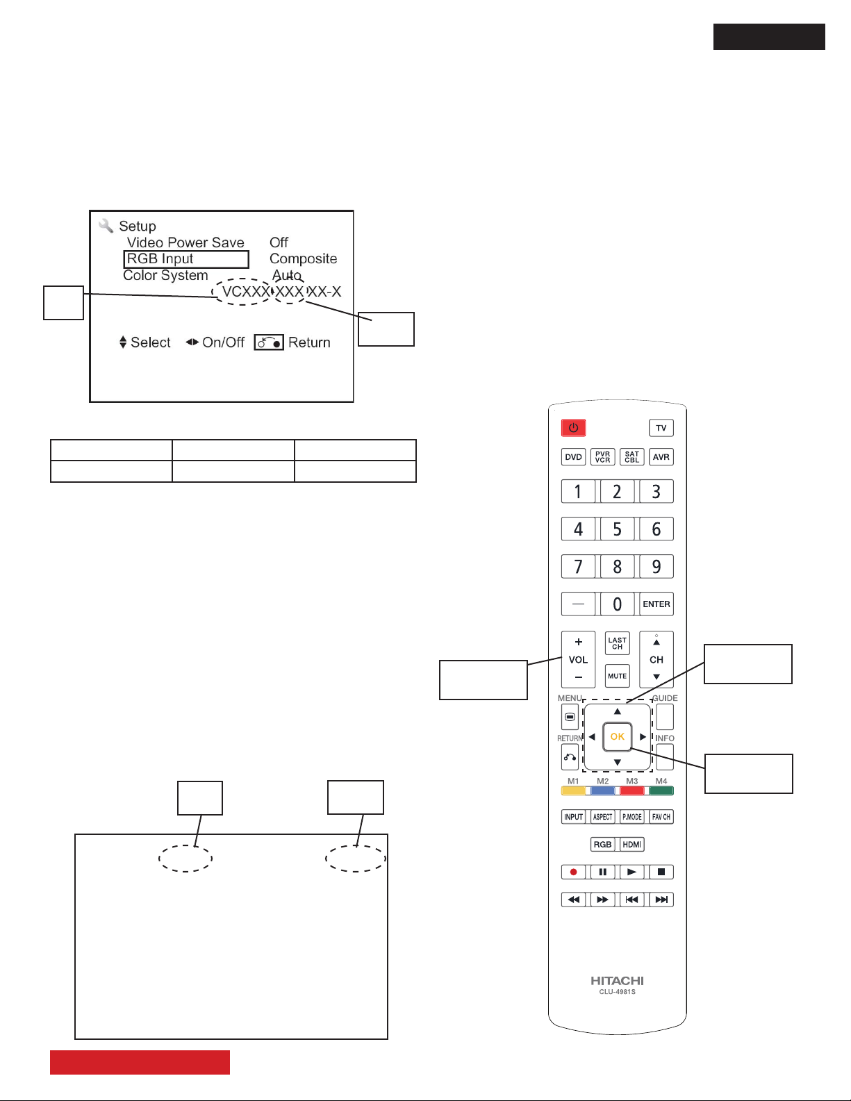
1.2 Changing data and selecting adjustment
codes.
When the UT monitor is in the Service Mode, use the remote
control cursor keys ◄, ►, ▲, ▼ to make the adjustments.
The bottom control panel in the UT monitor can also be used
for making the adjustments.
A. Use the Remote Control:
The ▲, ▼, keys are used for selecting the adjustment
item (in the same page).
The ◄, ► keys are used for changing the data values.
Use the VOL UP/DWN remote control button to scroll thru
the diferent Service Menu pages.
The “OK” button is equal to “Enter” key.
Next picture shows the R/C buttons mentioned in the previous explanation.
The software is subject to change, for the latest software call
1-800-HITACHI or log on to the Hitachi Service only web site
www.hitachiserviceusa.com.
1.1 How to get to the Service Mode Menu
The Service Mode Menu can be reached by following the
next sequence:
1. With TV in the off condition (with Main Power Off)
a) Press and hold Menu key of the bottom control panel,
while holding the menu key, press and release the master
power button.
b) Keep pressing the menu key until the Service Menu
appears on screen, release menu key.
2. To exit the Service Mode press [MENU] key of the remote
control or the UT monitor, the user menu OSD will appear.
The next picture shows the Service Mode OSD for the 42”
models(example).
Main
S/W
Sub
S/W
Service
NO. DATA VS224 42LW-A MU 146 Sub223
0: 208
1: 230
2: 237
3: 215
4: 224
5: 213
6: 223
7: 224
8: 187
9: 224
VOLUME
button
cursor
buttons
OK button
H: 33.6 V: 59.7 L: 562
TABLE OF CONTENTS
15
Page 17
D8MW
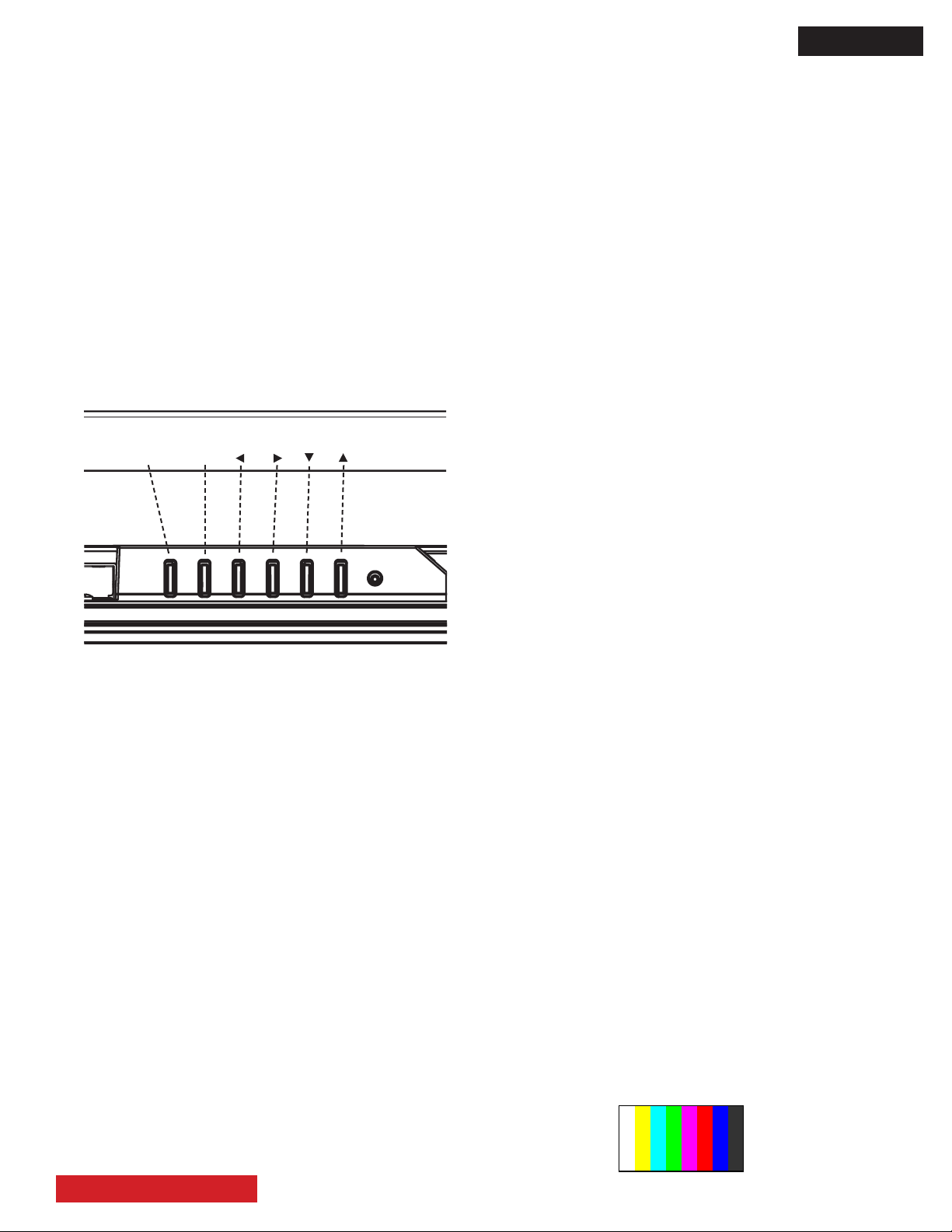
INPUT/OK
VOLMENU/EXIT
B. Use the Control Panel (located at the bottom):
Menu/Exit button is for calling the OSD menu or for exiting
such menu or any other OSD.
Input/Select button is for changing the displayed input or,
when some OSD is beeing displayed, to be able to select
the highlighted option.
◄ Vol - button is for reducing the audio volume or equiva-
lent to the Left cursor key when an adjustment value is
highlighted.
► Vol + button is for increasing the audio volume or
equivalent to the Right cursor key when an adjustment
value is highlighted.
▲ button is same as the R/C Up cursor button.
▼ button is same as the R/C Down cursor button.
The next gures show the labels of the bottom control panel
and a bottom view of the buttons.
2.2 EEPROM RENEW Procedure:
There are two methods.
FIRST METHOD.
(1) Enter Service Mode by the procedure in section 1.1.
(2) Change the data value of the adjustment item no. 659
from “0” to “1”.
(3) Push the OK button in the remote control. The picture will
disappear indicating that the initialization of the EEPROM is
started.
(4) About 2 seconds later, the initialization will nish and the
picture will appear again. Do not turn of the power until the
picture appears again.
(5) Set the adjustment item no. 630 to data value 6.
SECOND METHOD.
(1) Turn off the monitor by side panel power switch.
(2) Turn on the side panel power switch while keeping
pushed the up cursor key of the bottom control panel for
more than 5 seconds.
Conrm the settings are in factory shipping conditions (refer
to section 5.1 of this manual).
2.3 Memory initialize affected adjustments:
2. MEMORY INITIALIZE
The memory initialize operation is to clear the contents of
the data memory and to set all adjustment values to initial
default.
CAREFUL: The data that will be lost is shown in the section
no. “2.3 Memory initialize affected adjustments”.
2.1 EEPROM ALL INIT Procedure:
(1) Enter Service Mode by the procedure in section 1.1.
(2) Select adjustment item no. 657 and push the OK button
(the remote control must be set in normal TV mode).
The picture will disappear, and the initialization of the EE-
PROM will start.
The next table shows the adjustment items which are affected
by the Memory Initialize EEPROM ALL INIT operation and
EEPROM RENEW operation.
Adjustment ALL INIT RENEW
White balance Reset Not reset
Amplitude Reset Not reset
Item no. 657 Reset Not reset
3. VIDEO ADJUSTMENT
The next adjustments are related with the picture quality.
Special care must be put.
3.1 RGB amplitude adjustment (PC D-SUB input)
Adjustment preparations
(1) Turn on the UT monitor, allow a 20 minutes heat-run before beginning the adjustment.
(2) Input the PC VGA[60Hz] adjustment signal into the PC
D-SUB input terminal.
(3) The adjustment signal pattern is an 8 color bar. The black
should be at the pedestal level.
(3) About 2 seconds later, the initialization process will nish
and the picture will appear again. NOTE: Do not turn of the
(4) White level amplitude = 700 mV (100% of signal stan-
dard).
power until the picture appears again.
(4) Set the adjustment item no. 630 to data value 6.
TABLE OF CONTENTS
16
Page 18
D8MW
The next ghraphs show the waveform of the PC VGA[60Hz]
adjustment signal.
[mV]
700.0
Wh Ye Cy Gr Mg Re Bl Bk
G
0
-300.0
[mV]
700.0
Wh Ye Cy Gr Mg Re Bl Bk
B
0
[mV]
700.0
Wh Ye Cy Gr Mg Re Bl Bk
R
NOTE: Request this optional cable to Hitachi under the
next part numbers:
EW09192 - DSUB(LOW)-RCA CABLE 200MM
(4) The adjustment signal pattern is all white (The burst can
be disregarded).
(5) Set the amplitude of the adjustment signal [100% all
white] to 750.0 mV which is 105% (100% of the standard
signal is equal to 714.3 mV). The next graphics show the
white raster pattern and the waveform of the signal.
All white raster pattern.
[mV]
750.0
G
0
-300.0
White signal waveform.
0
Adjustment procedures
(1) Receive the PC adjustment signal.
(2) Select the adjustment item no. 658 of service adjustment
menu and push the OK button during 2 seconds or more.
The automatic adjustment will start.
(3) When the on screen display appears again, the automatic adjustment is nished.
3.2 NTSC Composite Video Adjustment
Adjustment Preparations
(1) Turn on the UT monitor and allow a 20 minutes heat-run
before starting the adjustment.
(2) Change the RGB input setting of the MENU’s second
page to “Composite”.
(3) Input the composite video adjustment signal into the
RGB D-SUB terminal. Consider the use of the next optional
cable.
EW09192
Adjustment Procedure
(1) Enter the Service Mode Menu by following the procedure
in section 1.1.
(2) Input the NTSC composite signal to the UT Monitor.
(3) Select the no. 658 adjustment item in the Service Mode
Menu and push the OK button for more than 2 seconds.
(4) The OSD will disappear for a brief moment. Once it appears again, the adjustment is nish.
(5) NOTE: Do not turn off the UT monitor until the OSD reappears.
4 VIDEO COLOR TEMPERATURE ADJUSTMENT.
The next adjustments are for setting the color coordinates or
color temperature of the picture.
4.1 Cool mode.
Adjustment preparations
(1) Adjustment signal: HDMI 1080i
Signal pattern: White raster.
Video level: 90%.
(2) Picture settings: Factory setting, check that the mode is
set as Factory shipping conditions.
Picture mode: Dynamic.
D-Sub 15 pin < ------- > RCA plug.
(3) The color analizer (CA-210) should be veried by a spectrum radiation brightness meter such as CS-1000 or stan-
The green color is connected.
TABLE OF CONTENTS
dard LCD.
17
Page 19
D8MW
(4) Set the aspect to full mode.
(5) Set the color analizer (CA-210) at the center of the pan-
el.
Adjustment procedures
(1) Enter the Service mode.
(2) Check that the adjustment items no. 0, no. 1 and no. 2
of the Service Mode menu have the next initial values. If the
initial values are different, set them as the following data.
No. 0 = 230
No. 1 = 230
No. 2 = 240
(3) Receive the white raster signal. Step down two (or only
one) of either of the R DRV_COOL, G DRV_COOL or B
DRV_COOL adjustment parameters and change to the
following values
(NOTE: At least one of the adjustment parameters should
remain in the initial data value).
4.2 Normal Mode.
Adjustment preparations
(1) Adjustment signal: HDMI 1080i
Signal pattern: White raster
Video level: 90%
(2) Picture settings: Factory setting. Check that the mode is
set as the factory shipping conditions.
Picture mode: Dynamic.
(3) The color analyzer (CA-210) should be veried by a
spectrum radiation brightness meter such as the CS-1000
or standard LCD.
(4) Set aspect to full mode.
(5) Set the color analyzer (CA-210) at the center of the pan-
el.
Adjustment procedures.
(1) Enter the Service mode by following the procedure in
section 1.1.
(2) Check that the initial data of the adjustment items no. 3,
4 and 5 are in the following values. If their initial values are
different, change them as shown.
Specication
Video Color Temperature (Cool)
x = 0.266 ± 0.005
y = 0.270 ± 0.005
14000K ± 0MPCD
REMARKS
(1) Color temperature should be adjusted under the condi-
tion in which the screen is the brightest, thus, the initial value
of the adjustment is set at its maximum.
This adjustment only decreases brightness.
(2) Beware, there is RESET in each picture mode.
(3) When the adjustment items no. 6, 7 or 8 are selected, the
color temperature of the picture changes to warm mode.
No. 3 = 224
No. 4 = 224
No. 5 = 224
(3) Receive the white raster signal. And decrease the value
of any two (or only one) of the R DRV_NORMAL, G DRV_
NORMAL or B DRV_NORMAL adjustment parameters in or-
der to get the X/Y coordinates to the following values.
Specication
Video Color Temperature (Normal)
x = 0.285 ± 0.005
y = 0.293 ± 0.005
9300K ± 0MPCD
REMARKS
(1) Color temperature should be adjusted under the condi-
tion in which the screen is the brightest, thus, the initial value
of adjustment is set at its maximum.
TABLE OF CONTENTS
(2) Beware there is RESET in each of the picture mode.
(3) When the adjustment items no. 6, 7 or 8 are selected, the
color temperature changes to warm mode.
18
Page 20

D8MW
4.3 Warm mode.
Adjustment preparations.
(1) Adjustment signal: HDMI 1080i
Signal pattern: White raster
Video level: 90%
(2) Picture settings: Factory shipping conditions.
Picture mode: Dynamic.
(3) The color analyzer (CA-210) should be veried by a
spectrum radiation brightness meter such as the CS-1000
or an LCD standard.
(4) Set the aspect to full mode.
(5) Set the color analyzer (CA-210) at the center of the pan-
el.
(6) Adjustment of color temperature cool mode and normal
mode should be nished.
Adjustment procedures.
(1) Enter the Service mode menu by following the procedure
in the section 1.1.
(2) Check that the initial data of the adjustment items no. 6,
7 and 8 are in the below shown values. If they are different,
change them to...
(4) Color temperature Warm synchronizes with the drive data
of the Normal mode color temperature. Therefore, when the
drive data of Normal color temperature is changed, the drive
data of the Warm color temperature is changed too.
5. Another procedure to set to Factory shipping
conditions
Adjustment procedures
(1) Turn off the power (Power indicator: Off)
(2) Push the ▲ key of the bottom control panel and turn on
the power of the UT monitor while keeping the up cursor key
pushed for more than 5 seconds.
(3) Verify the values of the factory shipping conditions according with the table in the next page.
(4) Set the adjustment item no. 630 to data value 6.
No. 6 = 224
No. 7 = 224
No. 8 = 224
(3) Receive the white raster signal. And decrease one or
two of the parameters R DRV_WARM, G DRV_WARM, or B
DRV_WARM in order to meet the X/Y coordinates with the
below values.
NOTE: At least one of the parameters should remain in the
initial value.
Specication
Video Color Temperature (Warm)
x = 0.313 ± 0.005
y = 0.329 ± 0.005
6500K ± 6.5MPCD
REMARKS
(1) Color temperature should be adjusted under the condi-
tion in which the screen is the brightest, thus, the initial value
of adjustment is set at its maximum.
(2) Beware there is RESET in each of picture mode.
(3) When the adjustment items no. 6, 7 or 8 are selected, the
color temperature of the picture changes to warm mode.
TABLE OF CONTENTS
19
Page 21
5.1 Factory shipping conditions:
D8MW
Item
Power Switch On (The switch is pushed condition.)
Volume 20
Mute Off
Picture Mode Dynamic
Contrast +31
Brightness 0
Color +3
Sharpness 0
Tint -1
Color Temperature Cool
Back Light +20
Deep Color Off
Contrast Mode Dynamic
3D Color Management On
Black Enhancement Middle
Picture
(HDMI/
Composite)
Picture
(RGB)
DNR Middle
MPEG NR Low
Cross Color NR Low
Game Mode Off
Film Mode Smooth2
3D Comb Filter Low
Amplitude Red 0
Color
Temp.
Adjus
Contrast +31
Brightness 0
Color 0
Tint 0
Color Temperature Normal
Amplitude Red 0
Color
Temp.
Adjust
Back Light +20
Green 0
Blue 0
Cut off Red 0
Green 0
Blue 0
Green 0
Blue 0
Cut off Red 0
Green 0
Blue 0
Initial data
42” UT monitor
Off
Off
Remarks
RGB
Input=Composite
only
TABLE OF CONTENTS
20
Page 22
5.1 ... factory shipping conditions continued.
D8MW
Item
Audio Treble +6
Bass +2
Balance 0
Surround Off
Bass Boost On
Clear Voice Off
Perfect Volume Off
Speakers On
Function System ― Grayed out
HDMI Control Auto Input Change Off
System Standby None
AV Center Control Off
Setup
(HDMI)
Setup
(RGB)
Language English (US)
Video Power Save Off
RGB Input RGB Grayed out
Color System Auto Grayed out
Auto Adjust ―
Horizontal Position 0
Vertical Position 0
Horizontal Clock 0
Clock Phase 0
Frequency Display On
WXGA Mode Off
RGB Input RGB
Initial data
42” UT monitor
Remarks
TABLE OF CONTENTS
21
Page 23

Page Left Blank
Instruction in software renewal
After software version up, set the following lists for reference.
D8MW
TABLE OF CONTENTS
22
Page 24

Page Left Blank
D8MW
TABLE OF CONTENTS
23
Page 25

Page Left Blank
D8MW
TABLE OF CONTENTS
24
Page 26

Page Left Blank
D8MW
TABLE OF CONTENTS
25
Page 27

Page Left Blank
D8MW
TABLE OF CONTENTS
26
Page 28

Page Left Blank
D8MW
TABLE OF CONTENTS
27
Page 29

TROUBLESHOOTING FLOWCHARTS
How to get to Burn-in mode
This mode displays the test patterns of some single color raster in turn. These signals are from built-in generator of panel. So it can be presumed that maybe the panel has some trouble when the screen of Burn-in
mode is abnormal.
Using the remote control with the set turned on can activate the mode.
(1) Set the service adjustment mode.
(2) Change No.646 from “0” to “1”. After a few second, appear the burn-in picture.
(3) To escape from this mode, change No.646 from “1” to “0”.
At rst, please conrm whether you put a connector cable again, and a phenomenon comes out.
[no picture, no sound]
LED is not light.
Is the voltage of
pin 5 (+5.4V) of CNPS
(power supply unit)
normal?
It is trouble of Main PWB
or Power supply unit.
Please change.
No
It is trouble of Main PWB or
Terminal PWB.
Picture trouble Go to “A”
Sound trouble Go to “B”
Yes
D8MW
TABLE OF CONTENTS
28
Page 30

...TROUBLESHOOTING FLOWCHARTS (continued)...
Is the burn-in
mode normal?
LED is green lighting.
Are the voltage of
pin 1-5 of CNPP1and pin 1-5 of
CNPP2 (power supply unit) normal?
Normal voltage is +24V.
It is trouble of Power supply
unit.
Please change.
No
Go to # 1
Yes
It is trouble of Main PWB or
Terminal PWB.
Picture trouble Go to “A”
Sound trouble Go to “B”
No
Yes
After a few seconds, it becomes
a red lighting even if it turns on
power.
Main PWB -- Inverter PWB
PPO1(pin 10) -- CN2(pin 12)
PPO1(pin 11) -- CN2(pin 14)
Are these connected?
No
It is trouble of Power supply unit.
Please change.
Or please check ELCD2 connector
or EPS connector.
Yes
It is trouble of Main PWB or LCD
panel (include Inverter PWB)
Please change.
D8MW
TABLE OF CONTENTS
29
Page 31

...TROUBLESHOOTING FLOWCHARTS (continued)...
# 1
Dose the backlight
turn on?
No
Yes
Are the voltage of
pin 1-4 (+12V) of PDO1
(Main PWB) normal?
It is trouble of
Main PWB.
Please change.
No
Yes
It is trouble of LCD
panel module.
No
Is there voltage of
pin 9 of CNPS
(Power supplyunit) ?
It is trouble of Main PWB.
Please change.
Yes
It is trouble of Inverter PWB.
D8MW
TABLE OF CONTENTS
30
Page 32

...TROUBLESHOOTING FLOWCHARTS (continued)...
A : Picture Troubleshooting
No picture, no color or dark
Check the picture menu.
Are there problems?
No
Yes
No
It is trouble of IR/PW-SW PWB.
Please check EISP connector
No
Are there
signals(R,G,B,H,V) at
CE12-CE14,RE49 and
RE50 of Main PWB?
Adjust the picture
menu.
Are the voltage of
pin 7 and 9 (+5V) of PV01
(Main PWB) normal?
Yes
RGB input
HDMI input
Are there
signals(R(8bit),G(8bit),
B(8bit),H,V,DE,CLK) at
RH33,RH35,RH37 and
RH39 of Main PWB?
It is trouble of IA01
of Main PWB.
Please change.
Are there
signals(R,G,B,H,V) at
CE06-CE08 and
IW01(pin1, 13) of Main
PWB?
It is trouble of QE01-QE03
or IE01of Main PWB.
Please change.
Yes
Yes
No
Yes
It is trouble of EFFC connector,
Terminal PWB, or PW01 of
Main PWB.
No
Are there signals(TMDS)
at RH60-67 of Main PWB?
It is trouble of IH01
of Main PWB.
Please change.
No
Is there voltage at
pin 18 (+5V) of JH01 (Main
PWB) and is there
voltage(over +2.4V) at
pin19 of JH01?
It is trouble of IH02
of Main PWB.
Please change.
It is trouble of Q001, GH01
or DH03 of Main PWB.
Please change.
Yes
No
Yes
D8MW
TABLE OF CONTENTS
31
Page 33

...TROUBLESHOOTING FLOWCHARTS (nished).
B : Sound Troubleshooting
No sound, abnormal sound
Is there signal
No
Yes
Yes
No
Yes
Check the signal at the P301
of Terminal PWB
Change speaker.
Has it been
improved?
It is trouble of
the speaker.
Change EISP cable
Change Terminal PWB
Has it been
improved?
It is trouble of the
Terminal PWB
Change EFFC cable
Has it been
improved?
Yes
It is trouble of the
EFFC cable.
No
Change Main PWB
D8MW
TABLE OF CONTENTS
32
Page 34

㪈㪏㪅㪋㪊㪉㪤㪟㫑
㪉㪇㪇㪏㪅㪇㪊㪅㪇㪌
㪝㪩㪚㩷㪧㫉㫆㪺㪼㫊㫊㪼㫉㩿㪰㪞㪫㪄㪇㪌㪈㪘㪀
㪝㪩㪚㩷㪧㫉㫆㪺㪼㫊㫊㪼㫉㩿㪰㪞㪫㪄㪇㪌㪈㪘㪀㪝㪩㪚㩷㪧㫉㫆㪺㪼㫊㫊㪼㫉㩿㪰㪞㪫㪄㪇㪌㪈㪘㪀
㪝㪩㪚㩷㪧㫉㫆㪺㪼㫊㫊㪼㫉㩿㪰㪞㪫㪄㪇㪌㪈㪘㪀
㪩㪏㪘㪇㪊㪇㪉㪎㪙㪞
㪩㪏㪘㪇㪊㪇㪉㪎㪙㪞㪩㪏㪘㪇㪊㪇㪉㪎㪙㪞
㪩㪏㪘㪇㪊㪇㪉㪎㪙㪞
㪣㪭㪛㪪㩷㪉㪺㪿
㪠㪉㪪㩷㫀㫅
㪩㪜㪪㪜㪫㩷㩷㩷㩷㩷㩷㩷㩷㩷㩷㩷㩷㩷㩷㩷㩷㩷㩷 㪝㪚㩷㪙㫌㫊
㪪㪬㪙㩷㪤㪧㪬
㪪㪬㪙㩷㪤㪧㪬㪪㪬㪙㩷㪤㪧㪬
㪪㪬㪙㩷㪤㪧㪬
㪤㪈㪍㪚㪆㪍㪋
㪤㪈㪍㪚㪆㪍㪋㪤㪈㪍㪚㪆㪍㪋
㪤㪈㪍㪚㪆㪍㪋
㪝㪚㪏㪶㪯㪩㪪㪫
㪫㫏㪃㩷㪩㫏㪃㩷㪚㪣㪢㪃㩷㪜㪥㪃㩷㪞㪶㪟㪙
㪞㪶㪯㪩㪪㪫
㪟㪆㪭㪶㪝㪩㪜㪨㪊
㪚㪜㪚
㪛㪛㪚
㪫㪤㪛㪪
㪚㪜㪚
㪉㫂㪹㫀㫋
㪜㪜㪧㪩㪦㪤
㪟㪛㪤㪠㩷㪩㫏
㪟㪛㪤㪠㩷㪩㫏㪟㪛㪤㪠㩷㪩㫏
㪟㪛㪤㪠㩷㪩㫏
㪪㫀㫃㪐㪈㪉㪌
㪪㫀㫃㪐㪈㪉㪌㪪㫀㫃㪐㪈㪉㪌
㪪㫀㫃㪐㪈㪉㪌
㪟㪛㪚㪧
㪫㪤㪛㪪
㪤㪘㪠㪥㩷㪪㪺㪸㫃㪼㫉㩷㪧㫉㫆㪺㪼㫊㫊㪼㫉
㪤㪘㪠㪥㩷㪪㪺㪸㫃㪼㫉㩷㪧㫉㫆㪺㪼㫊㫊㪼㫉㪤㪘㪠㪥㩷㪪㪺㪸㫃㪼㫉㩷㪧㫉㫆㪺㪼㫊㫊㪼㫉
㪤㪘㪠㪥㩷㪪㪺㪸㫃㪼㫉㩷㪧㫉㫆㪺㪼㫊㫊㪼㫉
㪝㪣㪠㪏㪌㪊㪏
㪝㪣㪠㪏㪌㪊㪏㪝㪣㪠㪏㪌㪊㪏
㪝㪣㪠㪏㪌㪊㪏
㪠㪉㪚㩿㪪㪚㪣㪈㪆㪪㪛㪘㪈㪀
㪰㪆㪞㪃㩷㪚㪹㪆㪙㪃㩷㪚㫉㪆㪩
㪛㪜㪃㩷㪚㪣㪢
㪟㪆㪭㪶㪪㪰㪥㪚
㪟㪛㪩㫏㪤㪬㪫㪜
㪠㪉㪪㩿㪘㪭㪪㪶㪠㪥㪀
㪠㪉㪪㩿㪜㪯㪫㪶㪠㪥㪀
㪧㪚㪄㪩㪃㩷㪞㪃㩷㪙
㪧㪚㪄㪟㪛㪃㩷㪭㪛
㪭㪞㪘㪶㪪㪚㪣㪆㪪㪛㪘
㪠㪉㪚
㪰㪆㪞㪃㩷㪚㪹㪆㪙㪃㩷㪚㫉㪆㪩
㪛㪜㪃㩷㪚㪣㪢
㪟㪆㪭㩷㪪㪰㪥㪚
㪠㪥㪫
㪠㪉㪪
㪤㪚㪣㪢
㪛㪛㪩㪋㪇㪇㩷㪪㪛㪩㪘㪤
㪛㪛㪩㪋㪇㪇㩷㪪㪛㪩㪘㪤㪛㪛㪩㪋㪇㪇㩷㪪㪛㪩㪘㪤
㪛㪛㪩㪋㪇㪇㩷㪪㪛㪩㪘㪤
㪉㪌㪍㪤㪹㫀㫋㫏㪉
㪝㫃㪸㫊㪿㩷㪤㪼㫄㫆㫉㫐
㪝㫃㪸㫊㪿㩷㪤㪼㫄㫆㫉㫐㪝㫃㪸㫊㪿㩷㪤㪼㫄㫆㫉㫐
㪝㫃㪸㫊㪿㩷㪤㪼㫄㫆㫉㫐
㪈㪍㪤㪹㫀㫋
㪍㪋㫂㪹㫀㫋㩷㪜㪜㪧㪩㪦㪤
㪍㪋㫂㪹㫀㫋㩷㪜㪜㪧㪩㪦㪤㪍㪋㫂㪹㫀㫋㩷㪜㪜㪧㪩㪦㪤
㪍㪋㫂㪹㫀㫋㩷㪜㪜㪧㪩㪦㪤
㪣㪭㪛㪪㪶㪪㪜㪣
㪣㪭㪛㪪㪉㪺㪿
㪙㪣㪶㪦㪥
㪜㪭㪦㪣㪶㪈
㪙㪣㪶㪛㪜㪫
㪪㪺㪿㫄㫀㫋㫋㪄
㪪㪺㪿㫄㫀㫋㫋㪄㪪㪺㪿㫄㫀㫋㫋㪄
㪪㪺㪿㫄㫀㫋㫋㪄
㪫㪩㪞㪅
㪫㪩㪞㪅㪫㪩㪞㪅
㪫㪩㪞㪅
㪉㫂㪹㫀㫋
㪜㪜㪧㪩㪦㪤
㪝㪚㩷㪙㫌㫊
㪫㫏㪶㪧㪛㪮㪥
㪫㫏㪃㩷㪩㫏
㪉㪊㪉㪚㪶㪪㪮㪈
㪢㪜㪰
㪣㪜㪛
㪧㪮㪣㪜㪛
㪠㪩㫀㫅
㪧㪮㪩㪪㪮㪄㪥
㪧㪦㪮㪜㪩㪈
㪪㪚㪣㪢
㪩㪜㪪㪜㪫
㪠㪩㫆㫌㫋
㪠㪩㫆㪽㪽
㪪㪮
㪪㪮㪪㪮
㪪㪮
㪫㪚㪋㪇㪍㪍㪙㪝㪫
㪫㪚㪋㪇㪍㪍㪙㪝㪫㪫㪚㪋㪇㪍㪍㪙㪝㪫
㪫㪚㪋㪇㪍㪍㪙㪝㪫
㪫㫏㪃㩷㪩㫏
㪫㫏㪃㩷㪩㫏
㪚㪦㪥㪫
㪉㪊㪉㪚㩷㪛㫉㫀㫍㪼㫉
㪉㪊㪉㪚㩷㪛㫉㫀㫍㪼㫉㪉㪊㪉㪚㩷㪛㫉㫀㫍㪼㫉
㪉㪊㪉㪚㩷㪛㫉㫀㫍㪼㫉
㪤㪘㪯㪉㪇㪉㪠㪧㪮
㪤㪘㪯㪉㪇㪉㪠㪧㪮㪤㪘㪯㪉㪇㪉㪠㪧㪮
㪤㪘㪯㪉㪇㪉㪠㪧㪮
㪚㪫㪪㪃㩷㪩㪫㪪
㪫㫏㪃㩷㪩㫏
㪩㪪㪄㪉㪊㪉㪚
㪩㪪㪄㪉㪊㪉㪚㪩㪪㪄㪉㪊㪉㪚
㪩㪪㪄㪉㪊㪉㪚
㪤㫀㫅㫀㪛㪠㪥㩷㪐㫇㫀㫅
㪪㪮
㪪㪮㪪㪮
㪪㪮
㪪㪥㪎㪋㪣㪭㪚㪈㪞
㪪㪥㪎㪋㪣㪭㪚㪈㪞㪪㪥㪎㪋㪣㪭㪚㪈㪞
㪪㪥㪎㪋㪣㪭㪚㪈㪞
㪪㩿㪤㪚㪣㪢㪶㪪㪜㪣㪀
㪙㪈㩿㪟㪛㪤㪠㪀
㪙㪉㩿㪧㪚㪀
㪘㪛㪚
㪘㪛㪚㪘㪛㪚
㪘㪛㪚
㪧㪚㪤㪈㪏㪇㪏
㪧㪚㪤㪈㪏㪇㪏㪧㪚㪤㪈㪏㪇㪏
㪧㪚㪤㪈㪏㪇㪏
㪣㪃㩷㪩
㪤㪚㪣㪢
㪛㪪㪧
㪛㪪㪧㪛㪪㪧
㪛㪪㪧
㪥㪡㪬㪉㪍㪇㪋㪈
㪥㪡㪬㪉㪍㪇㪋㪈㪥㪡㪬㪉㪍㪇㪋㪈
㪥㪡㪬㪉㪍㪇㪋㪈
㪠㪉㪪
㪩㪜㪪㪜㪫
㪛㪄㪘㪤㪧
㪛㪄㪘㪤㪧㪛㪄㪘㪤㪧
㪛㪄㪘㪤㪧
㪫㪘㪪㪌㪎㪇㪍
㪫㪘㪪㪌㪎㪇㪍㪫㪘㪪㪌㪎㪇㪍
㪫㪘㪪㪌㪎㪇㪍
㪧㪛㪮㪥
㪩㪜㪪㪜㪫
㪠㪉㪪
㪤㪬㪫㪜
㪤㪚㪣㪢
㪤㫀㫅㪧㫀㫅㪡㪸㪺㫂
㪤㫀㫅㪧㫀㫅㪡㪸㪺㫂㪤㫀㫅㪧㫀㫅㪡㪸㪺㫂
㪤㫀㫅㪧㫀㫅㪡㪸㪺㫂
㪧㪚㩷㪘㫌㪻㫀㫆
㪘㫌㪻㫀㫆㩷㪪㪮㪆㪛㪼㫃㪸㫐
㪣㩷㫆㫌㫋
㪩㩷㫆㫌㫋
㪣㪧㪣㩷㪋㪉㪭㩷㪝㪟㪛㩿㪈㪉㪇㪀
㪣㪧㪣㩷㪋㪉㪭㩷㪝㪟㪛㩿㪈㪉㪇㪀㪣㪧㪣㩷㪋㪉㪭㩷㪝㪟㪛㩿㪈㪉㪇㪀
㪣㪧㪣㩷㪋㪉㪭㩷㪝㪟㪛㩿㪈㪉㪇㪀
㪂㪈㪉㪭
㪣㪭㪛㪪㪶㪪㪜㪣
㪣㪭㪛㪪
㪣㪭㪛㪪
㪣㪭㪛㪪
㪣㪭㪛㪪
㪉㪋㪭
㪙㪣㩷㪦㪥
㪙㪩㪫
㪙㪣㪶㪝㪘㪠㪣
㪚㪫㪪㪃㩷㪩㪫㪪
㪫㫏㪃㩷㪩㫏
㪠㪉㪪㩿㪛㪼㫃㪸㫐㩷㫆㫌㫋㪀
㪟㪧㪶㪛㪜㪫
㪟㪧㪶㪤㪬㪫㪜
㪫㫏㪃㩷㪩㫏㪃㩷㪚㪣㪢㪃㩷㪜㪥㪃㩷㪞㪶㪟㪙
㪩㪜㪪㪜㪫
㪘㪬㪛㪶㪩㪜㪪㪜㪫
㪘㪬㪛㪶㪤㪬㪫㪜
㪘㪬㪛㪶㪪㪜㪣
㪪㪚㪣㪉㪆㪪㪛㪘㪉
㪪㪚㪣㪉㪆㪪㪛㪘㪉
㪪㪚㪣㪈㪆㪪㪛㪘㪈
㪠㪉㪪
㪤㪚㪣㪢㩷㫆㫌㫋
㪢㪼㫐㪄㪙㪛
㪠㪩
㪧㫆㫎㪼㫉㩷㪬㫅㫀㫋
㪧㫆㫎㪼㫉㩷㪬㫅㫀㫋㪧㫆㫎㪼㫉㩷㪬㫅㫀㫋
㪧㫆㫎㪼㫉㩷㪬㫅㫀㫋
㪧㫆㫎㪼㫉㪈
㪉㪋㪭
㪪㪫㪙㪌㪭
㪧㫆㫎㪼㫉㩷㪦㪝㪝
㪙㪣㪶㪦㪥
㪙㪩㪫
㪙㪣㪶㪛㪜㪫
㪠㪉㪪
㪦㫌㫋
㪧㪮㪤㫋㫆㪛㪚
㪟㪧㩷㫆㫌㫋
㪟㪧㩷㫆㫌㫋㪟㪧㩷㫆㫌㫋
㪟㪧㩷㫆㫌㫋
㪤㫀㫅㫀㩷㪧㫀㫅㩷㪡㪸㪺㫂
㪪㪮
㪪㪮㪪㪮
㪪㪮
㪮㪛㪫
㪮㪛㪫㪮㪛㪫
㪮㪛㪫
㪩㪌㪈㪇㪍㪥㪉㪐㪈㪘
㪩㪌㪈㪇㪍㪥㪉㪐㪈㪘㪩㪌㪈㪇㪍㪥㪉㪐㪈㪘
㪩㪌㪈㪇㪍㪥㪉㪐㪈㪘
㪪㪚㪣㪢
㪩㪜㪪㪜㪫
㪩㪜㪪㪜㪫㩷㪪㪮
㪠㫅㫍㪼㫉㫋㪼㫉
㪤㪸㫀㫅㩷㪙㫆㪸㫉㪻
㪤㪸㫀㫅㩷㪙㫆㪸㫉㪻㪤㪸㫀㫅㩷㪙㫆㪸㫉㪻
㪤㪸㫀㫅㩷㪙㫆㪸㫉㪻
㪡㪘㪊㪇㪎㪈㪈㪆㪉
㪡㪘㪊㪇㪎㪈㪈㪆㪉㪡㪘㪊㪇㪎㪈㪈㪆㪉
㪡㪘㪊㪇㪎㪈㪈㪆㪉
㪫㪼㫉㫄㫀㫅㪸㫃㩷㪙㫆㪸㫉㪻
㪫㪼㫉㫄㫀㫅㪸㫃㩷㪙㫆㪸㫉㪻㪫㪼㫉㫄㫀㫅㪸㫃㩷㪙㫆㪸㫉㪻
㪫㪼㫉㫄㫀㫅㪸㫃㩷㪙㫆㪸㫉㪻
㪡㪘㪊㪇㪎㪉㪈㪆㪉
㪡㪘㪊㪇㪎㪉㪈㪆㪉㪡㪘㪊㪇㪎㪉㪈㪆㪉
㪡㪘㪊㪇㪎㪉㪈㪆㪉
㪩㪃㩷㪞㪃㩷㪙
㪟㪃㩷㪭
㪛㪛㪚
㪛㪄㫊㫌㪹
㪛㪄㫊㫌㪹㪛㪄㫊㫌㪹
㪛㪄㫊㫌㪹
㪈㪌㫇㫀㫅
㪈㪌㫇㫀㫅㪈㪌㫇㫀㫅
㪈㪌㫇㫀㫅
㪟㪛㪤㪠
㪟㪛㪤㪠㪟㪛㪤㪠
㪟㪛㪤㪠
㪩㪪㪉㪊㪉㪚
㪪㪚㪣㪉㪆㪪㪛㪘㪉
㪟㪧㩷㪘㪤㪧
㪟㪧㩷㪘㪤㪧㪟㪧㩷㪘㪤㪧
㪟㪧㩷㪘㪤㪧
㪥㪡㪮㪈㪈㪇㪐㪭
㪥㪡㪮㪈㪈㪇㪐㪭㪥㪡㪮㪈㪈㪇㪐㪭
㪥㪡㪮㪈㪈㪇㪐㪭
㪣㩷㫀㫅
㪩㩷㫀㫅
㪛㪘㪚
㪛㪘㪚㪛㪘㪚
㪛㪘㪚
㪮㪤㪏㪌㪉㪇
㪮㪤㪏㪌㪉㪇㪮㪤㪏㪌㪉㪇
㪮㪤㪏㪌㪉㪇
㪠㪉㪪
㪤㪬㪫㪜
㪩㪜㪪㪜㪫
㪤㪚㪣㪢
㪣㩷㫆㫌㫋
㪩㩷㫆㫌㫋
㪣㩷㫆㫌㫋
㪩㩷㫆㫌㫋
㪫㫏㩷㪃㪩㫏
㪧㪮㪄㪣㪜㪛
㪧㪮㪄㪪㪮
㪧㪮㩷㪚㫆㫅㫅㪼㪺㫋 㫆㫉
㪠㪩㪆㪧㪮
㪚㫆㫅
㪩㪃㪞㪃㪙㩷㪈㪺㪿
㪛㪜㪃㪚㪣㪢㪃㪟㪃㪭
㪩㪃㪞㪃㪙㪶㪈㪺㪿
㪠㪉㪪㩷㫆㫌㫋
㪛㪛㪩㪉
㪛㪛㪩㪉㪛㪛㪩㪉
㪛㪛㪩㪉
㪉㪌㪍㪤㪹㫀㫋㫏㪊
㪣㪭㪛㪪㩷㪫㫏
㪣㪭㪛㪪㩷㪫㫏㪣㪭㪛㪪㩷㪫㫏
㪣㪭㪛㪪㩷㪫㫏
㪫㪟㪚㪍㪊㪣㪭㪛㪈㪇㪉㪊
㪫㪟㪚㪍㪊㪣㪭㪛㪈㪇㪉㪊㪫㪟㪚㪍㪊㪣㪭㪛㪈㪇㪉㪊
㪫㪟㪚㪍㪊㪣㪭㪛㪈㪇㪉㪊
㪩㪃㪞㪃㪙
㪛㪜㪃㪚㪣㪢㪃㪟㪃㪭
㪫㪯㪶㪧㪛㪮㪥
㪣㪭㪛㪪㩷㪈㪺㪿
㪣㪭㪛㪪㪶㪈㪺㪿
㪣㪭㪛㪪㩷㪈㪺㪿
㪣㪭㪛㪪㪶㪈㪺㪿
㪣㪭㪛㪪㩷㪚㫆㫅㫅㪼 㪺㫋㫆㫉㪉 㪣 㪭㪛㪪㩷㪚㫆㫅㫅㪼㪺 㫋㫆㫉㪈
㪉㪋㪭
㪣㪜㪛
㪣㪭㪛㪪㩷㪫㫏
㪣㪭㪛㪪㩷㪫㫏㪣㪭㪛㪪㩷㪫㫏
㪣㪭㪛㪪㩷㪫㫏
㪫㪟㪚㪍㪊㪣㪭㪛㪈㪇㪉㪊
㪫㪟㪚㪍㪊㪣㪭㪛㪈㪇㪉㪊㪫㪟㪚㪍㪊㪣㪭㪛㪈㪇㪉㪊
㪫㪟㪚㪍㪊㪣㪭㪛㪈㪇㪉㪊
㪛㪜㪃㪚㪣㪢㪃㪟㪃㪭
㪩㪃㪞㪃㪙
㪫㫏㪶㪧㪛㪮㪥
㪛㫆㫋㫋㪼㪻㩷㫃㫀㫅㪼㪑㩷㪥㫆㩷㫌㫊㪼㩷㫆㫉㩷㪥㫆㫋㩷㫄㫆㫌㫅㫋
㪣㪭㪛㪪㩷㪈㪺㪿
㪣㪭㪛㪪㪶㪈㪺㪿
BLOCK DIAGRAMS
42” UT Monitor.
D8MW
TABLE OF CONTENTS
33
Page 35

3
2
1
PSPK
PA-04H
1
2
3
4
PPU1
VH-03V-D(#2NC)
1
NC
3
PZ01
GH-03H
1
2
3
G1
G2
PM01
SH-10H
1
2
3
4
5
6
7
8
9
10
G1
G2
CNPP2
PH-12H
1
2
3
4
5
6
7
8
9
10
11
12
G1
G2
J001
1
L
2
N
3
FG
F.G
E902
F.G
P801
501568-04H
123
4
G1
G2
P602
501568-04H
123
4
G1
G2
P601
501568-06H
12345
6
G1
G2
PV02
501568-06H
1
2
3
4
5
6
G1
G2
CNPP1
PH-14H
1
2
3
4
5
6
7
8
9
10
11
12
13
14
G1
G2
PNPS
PA-11H
1234567891011
G1
G2
PP01
PA-11H
1234567891011
G1
G2
CNAC
1
2
3
PM02
SH-10H
1
2
3
4
5
6
7
8
9
10
G1
G2
PL02
FIR-4 1H
123456789
10111213141516171819202122232425262728293031323334353637383940
41
G1G2G3G4G5
G6
G7G8G9
G10
PL01
FIR-5 1H
123456789
101112131415161718
1920212223242526272829303132333435363738394041
G1
G2G3G4G5G6
G7G8G9
G10
424344454647484950
51
PW02
FH28- 50HL ow
12345678910111213141516171819202122232425262728293031323334353637383940414243444546474849
50
G1
G2
P102
FH28- 50HL ow
12345678910111213141516171819202122232425262728293031323334353637383940414243444546474849
50
G1
G2
PW01
50156 8-14 H
12345678910111213
14
G1
G2
P101
50156 8-14 H
12345678910111213
14
G1
G2
PV01
501568-10H
1
2
3
4
5
6
7
8
9
10
G1
G2
P701
501568-10H
1
2
3
4
5
6
7
8
9
10
G1
G2
CN1
PH-14H
1
2
3
4
5
6
7
8
9
10
11
12
13
14
G1
G2
CN2
PH-12H
1
2
3
4
5
6
7
8
9
10
11
12
G1
G2
Main P.W.B.
JA30711/2
POWER P.W.B.
Terminal P.W.B.
JA30721/2/3-A/B
Filter P.W.B.
Control P.W.B.
IR/PWR_SW
P.W.B.
Speaker
Lout-N
Lout-P
Rout-N
Rout-P
+24V
POWER 1
GND
STB5V
POWER OFF
GND
AC CL OCK
BRT
BL ON (ON /OFF )
+24V
+24V
AC CL OCK
BRT
BL ON (ON /OFF )
+24V
STB5V
POWER OFF
GND
GND
POWER 1
FANLOCK
FANVCC
GND(FAN)
(to FAN)
LVDS (to T-CON LCD UNIT) ECN1
SUBuCON I/F
AC
AC
AC
AC
+24V
+24V
+24V
+24V
+24V
GND
GND
GND
GND
GND
BRT
BL_ON(ON OFF)
EPS
EPU
ELS
(EJS)
AC cord
E001
AMP-IN 1P
ADKEY 1
USRRS T
ADKEY 2
GND
ADKEY 2
LED P.W.B.
ADKEY 1
USRRS T
GND
PWERL ED0
STB+5 V
ADKEY 1
USRRS T
ADKEY 2
GND
EKL
3.14.1
NC
DVR-03V-S
E002
EISP
BL_DE T
BL_DE T
STB+5V
ADKEY2
LEDB
ADKEY1
GND
USRRST
SUBuCON I/F
(EJS)
GND
SUB_RXD
S_BUSY
STB+3.3V
S_SCLK
SUB_TXD
S_CNVSS
S_RESET
GND
S_SCLK
SUB_TXD
S_CNVSS
S_RESET
GND
GND
SUB_RXD
S_BUSY
STB+3.3V
TD2-
GND
GND
GND
NC.
TA2-
TA1-
NC.(E XT_V BR)
TD2+
GND
NC.
TC1-
VDD
GND
TE1-
TE2-
TB1+
VDD
TCLK2 -
NC.
GND(L VDS)
TB2+
TC2+
TE1+
GND
TB1-
GND
TC2-
NC.
TCLK2 +
VDD
NC.
TE2+
TD1+
GND
NC.(D CR)
TD1-
GND
LVDSS EL
TC1+
GND
TCLK1 +
TCLK1 -
GND
TA1+
TB2-
NC.(V BR_o UT)
TA2+
GND(L VDS)
VDD
NC.
NC.
TA4-
NC.
GND
NC.
TCLK4 +
TCLK3 +
NC.
TCLK4 -
TD4-
GND
NC.
TC4-
NC.
GND
GND
TC3+
TE3+
TA3-
TE4+
TD3-
GND
GND
TD4+
TA3+
GND
TB4+
TE3-
TD3+
TE4-
TC4+
NC.
TB3-
TB4-
TB3+
TA4+
NC.
GND
TC3-
TCLK3 -
GND
PWRSW_N
LEDG
PWON+3.3V
GND
STB+5V
PoWER1_SW
LEDo
LEDR
PoWER1
iR_iN
LVDS (to T-CON LCD UNIT) ECN2
EMT1 EMT2
SPR
EIIV
Inverter
Master
Inverter
Slave
ELCD2
ELCD3
LCD Panel
SPL
EIP1
EIP1
CN5
CN6
CN3
CN4
+24V
+24V
+24V
+24V
+24V
GND
GND
GND
GND
GND
BRT
BL_ON(ON OFF)
NC
BL_DET
CONNECTIONS DIAGRAM
42” UT Monitor.
D8MW
TABLE OF CONTENTS
34
Page 36

'%0
'%0
'++8
'+2
'+52
'-.
'+2
'.%& '.%&
'.5
'/6
'/6
'25
'
27
D8MW UT42 Wiring Dress DWG
㪥㪜㪣㪪㩷
㪥㪪㪧㪢㪉 㪥㪪㪧㪢㩷
㪥㪠㪪㪈㩷
0
㶎㪈㩷³(36DQG³(/&'´PXVWSDVVRQ³(&1´DQG³(&1´㩷
㶎㪉㩷'RWKHVW\OLQJVRWKDWWKHELQGLQJWDSHRI³(/&'´DQG³(/&'´VKRXOGQRWWRXFKWKHPDLQIUDPH.㩷
㶎㪉
㶎㪊㩷'RWKHVW\OLQJVRWKDWWKHZLUHVKRXOGQRWWRXFKWKHPDLQ3:%VVKLHOGLQJFDVH㩷
㶎㪋㩷
7DNHORRVHQLQJRIWKH³(,63´ZLUHVRWKDWDORQJWKHJXLGHRI%H]HODVV¶\
'RWKHVW\OLQJVRWKDWWKHZLUHVKRXOGQRWWRXFKWKH
$&VZLWFK
㩷
㶎㪌㩷'RWKHVW\OLQJVRWKDWWKH(,63ZLUH
DORQJWKHJXLGHRI%H]HODVV¶\
㩷
㩷 1LWWRW DSH1R
: PP/ PP㩷
㩷 1LWWRW DSH1R
: PP/ PP㩷
㩷 '0:6 ,*1$/
6/'7 $3(㩷
㩷 '0:6,*1 $/
6/'7 $3(㩷
㩷 1LWWRW DSH1R
: PP/ PP㩷
㶎㪈
㶎㪊
㶎㪉
㶎㪌
㩷 1LWWRW DSH1R
: PP/ PP㩷
㶎㪌
㶎㪋㩷
㩷 1LWWRW DSH1R
: PP/ PP㩷
0'%0
㪜07
1LWWRWDSH1R
: PP/ PP
Wiring Diagram page 1/6
D8MW
TABLE OF CONTENTS
35
Page 37

䇼
Pre-operation䇽㩷
㪈
㩷 Set the ferrite core(NECN1) to ECN1.
NECN1 MAG K5BFP 40X2X12-K
(P#GX00821)
#WN03 Nitto tape No.5
W=20mm L=70mm
ECN1
Wiring Diagram page 2/6
D8MW
TABLE OF CONTENTS
36
Page 38

㪉㩷 Set the ferrite core(N001) to EMT2.
䇼
Pre-operation䇽㩷
㪥㪇㪇㪈㩷
㪜㪤㪫㪉㩷
㪓㪄㪄㩷 㪤㪸㫀㫅㩷 㪧㪮㪙㩷 㫊㫀㪻㪼㩷
㪫㪼㫉㫄㫀㫅㪸㫃㩷 㪧㪮㪙㩷 㫊㫀㪻㪼㩷 㪄㪄㪕
ޣ
surface
ޤ
Ferrite core is 1set by 2pcs.
㪌㫄㫄㫧㪈㫄㫄
㩷
#WN01 Nitto tape No.5
W=20mm L=70mm
㪓㪄㪄㪫㪼㫉㫄㫀㫅㪸㫃㩷 㪧㪮㪙㩷 㫊㫀㪻㪼㩷
㪤㪸㫀㫅㩷 㪧㪮㪙㩷 㫊㫀㪻㪼㪄㪄㪕㩷
ޣ
reverse
ޤ
ޣsideޤ
㪓㪄㪄㩷 㪤㪸㫀㫅㩷 㪧㪮㪙㩷 㫊㫀㪻㪼
㪫㪼㫉㫄㫀㫅㪸㫃㩷 㪧㪮㪙㩷 㫊㫀㪻㪼㩷 㪄㪄㪕㩷
Wiring Diagram page 3/6
D8MW
TABLE OF CONTENTS
37
Page 39

Paste to N001 Paste to near ECN1
㪊㩷 How to paste of #333 (D8MW SIGNAL SLD TAPE P#MD20801)㩷
ECN1
㪋㪅㩷 㩷 㪟㫆㫎㩷 㫋㫆㩷 㫊㫋㫐㫃㫀㫅㪾㩷 㵰㪜㪠㪪㪧㵱㩷 㫎㫀㫉㪼㩷 㫋㪿㪸㫋㩷 㪪㪧㪣㩷 㫊㫀㪻㪼㪅㩷
㩷 㩷 㩷 㩷
052-
#333 dose not touch the “NECN1” .
Separate 1mm or more.
#333
1mm or more
#333
Black tape
EISP wire
Guide of bezel
3mm or less
Speaker L
NECN1
#WN04 Nitto tape No.5
W=9mm L=30mm
N001
Wiring Diagram page 4/6
D8MW
TABLE OF CONTENTS
38
Page 40

Wiring Diagram page 5/6
㪌㩷 How to set the ferrite core(NELS) to ELS.㩷
㪜㪣㪪㩷
㪍㪇㫄㫄㫧㪌㫄㫄
㪍How to set the ferrite core(NSPK, NSPK2) to EISP.㩷
㪜㪠㪪㪧㩷
㪌㪇㫄㫄㫧㪌㫄㫄
㪉㪇㫄㫄㫧㪌㫄㫄
Main PWB side
LED PWB side
NELS MAG K5CRC12X15X7-MB2
(P# GX00738)
1 turn
SP R side
Main PWB side
Terminal PWB side
Binding tape
Binding tape
NSPK2 MAG K5CRC12X15X7-MB2
(P# GX00738)
1 turn
SP L side
NSPK MAG K5CRC12X15X7-MB2
(P# GX00738)
1 turn
D8MW
TABLE OF CONTENTS
39
Page 41

Wiring Diagram page 6/6
㪎㩷 Paste #327 so that ECN1, ECN2 should not float.
'%0
'
%0
#327
Nitto tape No.5
W=20mm L=100mm
㩷
㪏㩷 How to set the ferrite core NEPU㩷 to EPU.
20mm
25mm
78mm or more
NEPU MAGK5CRC16X28X9-M2G2
(P# GX00732)
Put on the core with fit.
ኒ⌕ߐߖࠆ
#NEPU SK-binder
(P#:3763751)
D8MW
TABLE OF CONTENTS
40
Page 42

Final assembly guide411/9
D8MW
TABLE OF CONTENTS
Page 43

Final assembly guide
2/9
D8MW
TABLE OF CONTENTS
42
Page 44

Final assembly guide
3/9
D8MW
TABLE OF CONTENTS
43
Page 45

Final assembly guide
4/9
D8MW
TABLE OF CONTENTS
44
Page 46

Final assembly guide
5/9
D8MW
TABLE OF CONTENTS
45
Page 47

Final assembly guide
6/9
D8MW
TABLE OF CONTENTS
46
Page 48

Final assembly guide
7/9
D8MW
TABLE OF CONTENTS
47
Page 49

Final assembly guide
8/9
D8MW
TABLE OF CONTENTS
48
Page 50

Final assembly guide
9/9
D8MW
TABLE OF CONTENTS
49
Page 51

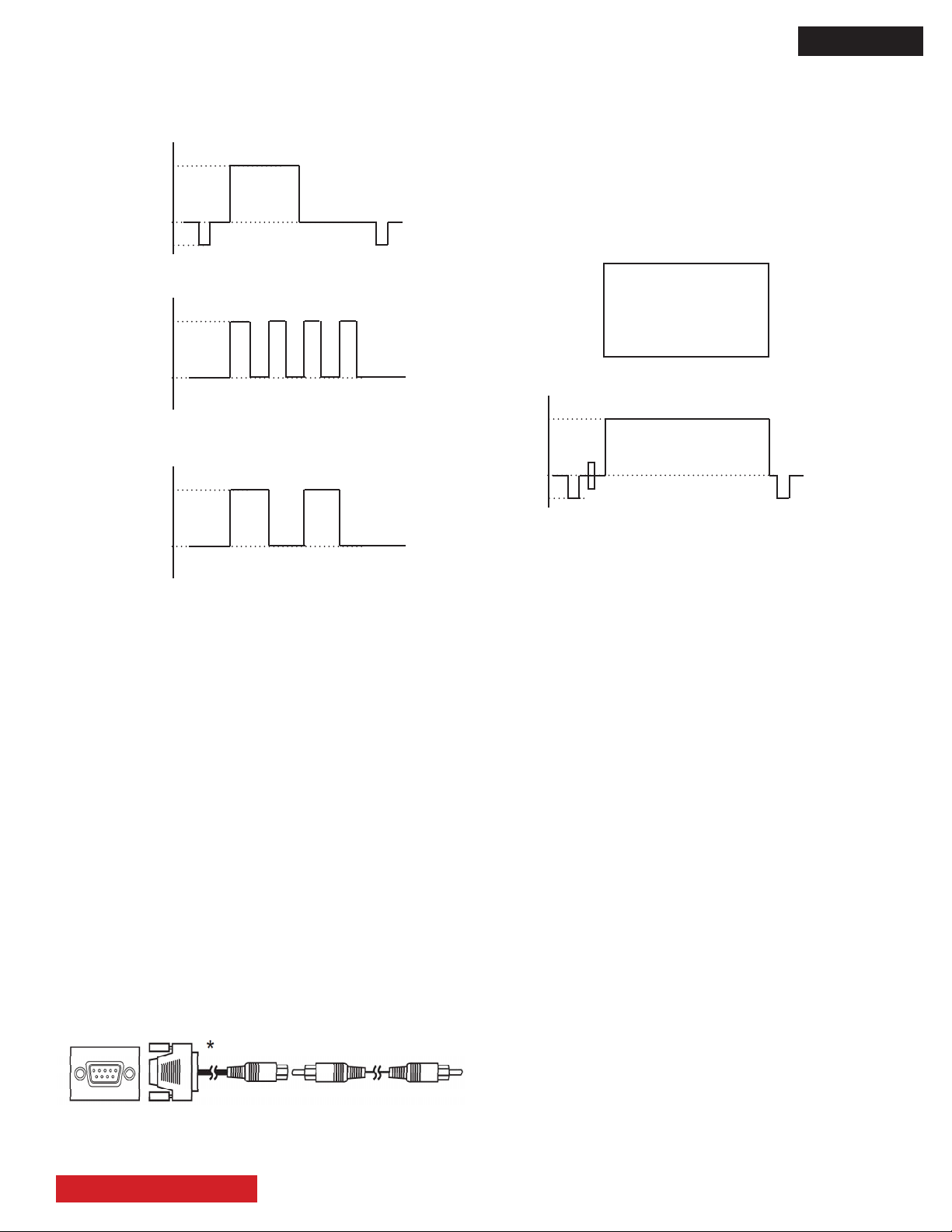
WAVEFORMS
The number icons thru the circuit schematic are reference to the next waveforms.
The waveforms were taken with a color bar video signal and for the audio a 1Vp-p 1kHz audio signal was used.
PC video signal white icon numbers, example
HDMI video signal, black icon numbers, example: .
. PC signal, green color @ CE12 (page 62) . PC signal, blue color @ CE13 (page 62)
D8MW
. PC signal, red color @ CE14 (page 62) . PC signal, horizontal drive@ RE49 (page 62)
. PC signal, vertical drive @ RE50 (page 62) . PC signal, green color @ CE06 (page 62)
TABLE OF CONTENTS
50
Page 52

... WAVEFORMS (continued)
. PC signal, blue color @ CE07 (page 62) . PC signal, red color @ CE08 (page 62)
. PC signal, sub-vertical drive @ IW01 pin 1 (page 72) . PC signal, sub-horiz. drive @ IW01 pin 13 (page 72)
D8MW
. HDMI signal, HDMI-CLK @ RH33 (page 63) . HDMI signal, HDMI CB @ RH35 (page 63)
TABLE OF CONTENTS
51
Page 53

... WAVEFORMS (continued)
D8MW
. HDMI signal, HDMI-Y @ RH37 (page 63)
. HDMI signal, RX @ RH60~RH67 (page 63)
. HDMI signal, HDMI CB @ RH35 (page 63)
. Audio signal, Input @ R225 (page 74)
. Audio signal, output @ P301 (page 75)
TABLE OF CONTENTS
52
Page 54

D8MW
DC VOLTAGES
To allow a quick check, the next table shows the direct current voltages of the most accesible connector terminals in the
LCD UT monitor.
BOARD CONNECTOR
TERMINAL
MAIN PV01 0 3.2 0 5.2 0 0 3.1 5.2 5.3 0.2 - - - -
PP01 23.8 23.8 0 0 5.3 0 3 3.2 3.3 3.3 0.2 - - -
P101 0 0 10.8 10.8 10.8 10.8 0 0 5.5 55 0 0 5.3 0
IR/PWR_SW P701 0 3.2 0 5.2 0 0 3.1 5.2 5.3 0.2 - - - POWER CNPS 23.8 23.8 0 0 5.3 0 3 3.2 3.3 3.3 0.2 - - -
CNPP1 23.8 23.8 23.8 23.8 23.8 0 0 0 0 0 3.2 3.3 0.2 0.2
CNPP2 23.8 23.8 23.8 23.8 23.8 0 0 0 0 0 3.2 3.3 - -
1 2 3 4 5 6 7 8 9 10 11 12 13 14
TABLE OF CONTENTS
53
Page 55

Schematic Diagram page /28
17
RS232C
18
RS232C I/F
FC8 FC8
16
DDR2 I/F
FC8
20
15
iR Out
13
Power
Connector
19
etc
14
SiI 9125
12
HDMI Rx
10
SubMPU
M16C64
11
LVDS Out
GENESIS
DDR I/F
09
GENESIS
07
GENESIS
HDMI-iN
RGB-iN
08
OCM I/F1
GENESIS
Power
06
GENESIS
04
GENESIS
OCM I/F2
Flash Rom
05
FAN,OVP
FAN,
Protection
03
POWER
Main Power
DCDC Reg.
02
Block
Diagram
01
Sheet Page Reference
Block Diagram
D8MW 42V FHD UT LCD Panel
CEC
DDR Memory
Flash
Memory
EEPROM
DDC
DDC
EEPROM
EEPROM
TxRx
Bus SW
I2S
I2S
LVTTL
LVDS
I2S
I2S
I2C
Analog
RGB
L,R
+24V
STB+5V
CEC
UART
FC-Bus
232C
Tranciever
TMD S
Audio
DSP
I2S
LVD S
FAN VCC
Key Switch
LED
iR
LVDS + Control + etc
Audio
ADC
RS232CiR Out
Audio
AMP
Audio In
Mini Jack
Analog
RGB In
HDMI In
Sub MPU
Renesas
M16C64
DDR2
Memory
DDR2
Memory
DDR2
Memory
DDR Memory
HDMI Rx
Silicon Image
SiI9125
FC8
Scaler IC
Genesis
FLI8538-LF
Signal PWB
AC-inlet
42 LCD Panel(LPL)
CONT PWB
Filter PWB
Power PWB
(Reserve)
(Reserve)
Connector
Terminal PWB
IR PWB
Power SW
Speaker
Stereo Out
I2S
Power LED
LED PWB
LVDS Tx
THC63LVD1023
LVDS Tx
THC63LVD1023
LVTTL
(1st)
LVTTL
(2nd)
LVDS
(3rd)
LVDS
(1st)
LVDS
(2nd)
LVDS
(4th)
Connector
LVDS Tx
LVDS
Signal Board Circuit
Main :JA30712
Terminal :JA30723
1
3 4
5
6
7
D8MW
A
B
C
D
E
TABLE OF CONTENTS
• Since this is a basic circuit diagram, the value of the parts is subject to be altered for improvement.
54
F
MAIN BOARD SHEET: 001
Block Diagram
Page 56

Schematic Diagram page /28
4
5
3
2
1
G1
5
6
7
8
4
3
2
1
G1
5
6
7
8
4
3
2
1
G1
5
6
7
8
4
3
2
1
G1
5
6
7
8
4
3
2
1
G1
5
6
7
8
4
3
2
1
CP82
2125
22/6.3
1
2
CP26
3225
4.7
1
2
CP61
0.01
1
2
CP54
0.1
1
2
CP67
0.01
1
2
CP69
0.01
1
2
CP92
2125
22/6.3
1
2
CP66
0.01
1
2
CP52
0.1
1
2
CP62
0.01
1
2
CP51
0.1
1
2
CP64
0.01
1
2
CP53
0.1
1
2
CP84
1.0/16
1
2
CP24
3225
4.7
1
2
CP85
4.7/6.3
1
2
CP55
0.1
1
2
CP30
3225
4.7
1
2
CP56
0.1
1
2
CP50
0.1
1
2
CP99
1005
0.01/25
1
2
CP98
1005
0.01/25
1
2
CP83
1005
0.01/25
1
2
CP97
1005
0.01 /25
1
2
CP95
1005
0.01 /25
1
2
CP35
3225
22/16
1
2
CP36
3225
22/16
1
2
CP21
3225
4.7
1
2
CP22
3225
1.0
1
2
CP71
1005
0.047/16
1
2
CP72
1005
0.047/16
1
2
CP74
1005
0.047/16
1
2
CP87
1.0/16
1
2
CP86
1.0/16
1
2
CP60
0.1
1
2
CP39
3225
22/16
1
2
CP28
3225
4.7
1
2
CP59
0.1
1
2
CP68
0.01
1
2
CP40
3225
22/16
1
2
CP73
1005
0.047/16
1
2
CP63
0.01
1
2
CP38
3225
22/16
1
2
CP58
0.1
1
2
CP75
1005
0.047/16
1
2
CP70
0.01
1
2
CP65
0.01
1
2
CP57
0.1
1
2
CP96
1005
0.01 /25
1
2
CP32
3225
4.7
1
2
CP37
3225
22/16
1
2
CP13
100/16
MVK/SKV
1
2
CP11
100/16
MVK/SKV
1
2
CP10
100/16
MVK/SKV
1
2
CP12
100/16
MVK/SKV
1
2
DP02
M2FM3
1
2
DP03
M2FM3
1
2
DP01
M2FM3
1
2
DP04
M2FM3
1
2
DP05
M2FM3
1
2
IP10
TK11133CSC
Vcont
GND
Np Vout
Vin
GND1
GND1
GND1
GND1
GND1
GND1
GND1
GND1
GND1
GND1
GND1
GND1
GND1
GND1
GND1
GND1
GND1
GND1
GND1
GND1
GND1
GND1
GND1
GND1
GND1
GND1
GND1
GND1
GND1
GND1
RP15
1.0k
1
2
RP10
0
1
2
RP51
12k
1
2
RP02 0
1
2
RP54
10k-1%
1
2
RP53
0
1
2
RP09
1.0k
1
2
RP01 0
1 2
RP04
5.6k
1
2
RP63
0
1
2
RP35
27k-1%
1
2
RP64
10k-1%
1 2
RP65
75k-1%
1
2
RP36
4.7k-1 %
1
2
RP34
10k-1%
1
2
RP60
47k
1
2
RP43
0
1
2
RP30
47k
1
2
RP61
12k
1
2
RP46
47k-1%
1
2
RP66
560-1%
1 2
RP44
10k-1%
1
2
RP50
47k
1
2
RP25
4.7k-1 %
1
2
RP45
82k-1%
1
2
RP31
12k
1
2
RP23
0
1
2
RP33
0
1 2
RP24
10k-1%
1
2
RP41
12k
1
2
RP07
1.0k
1
2
RP40
47k
1
2
RP55
11k-1%
1
2
RP08
1.0k
1
2
RP56
130k-1%
1
2
RP06
1.0k
1
2
RP26
56k-1%
1
2
ACCLK
012:1E
TV_POWER
009:1C
012:1D
+5.6V
003:G4
004:2A
008:4A
009:1C
011:1B
012:1A
015:2A
016:1A
020:2B
STB+5V
012:4E
012:8E
013:5C
014:2B
014:2D
015:2A
020:2C
020:5D
D+3.3V
003:C6
003:G4
004:2E
005:1C
006:1A
009:1A
011:1
A
016:1A
017:1A
017:6C
019:3E
019:4A
019:4D
019:6A
019:6D
020:4E
PWR_OFF
005:1E
012:1E
020:4C
020:4D
020:7D
STB+3.3V
012:1A
013:5B
014:2B
PON_TCON
012:1D
POWER2TD
012:1D
015:2B
016:1B
020:2C
PON_3.3V
012:8B
016:1C
PON_5.6V
012:1D
PON_PSU013:5D
BRT
008:7B
Tcon+12V
003:G5
019:6C
BL_oN
005:7D
FAN_EN
012:8B
FANVCC
003:C7
AMP_PWR
003:G6
020:2B
STB+5V
STB+3.3V
Tcon+12V
D+3.3V
+5.6V
AMP_PWR
FANVCC
CP81
3225
22/16
1
2
CP91
3225
22/16
1
2
CP76
1005
3300p
1
2
RP22
10k
1
2
RP62
10k
1
2
CP77
1005
3300p
1
2
CP80
1005
3300p
1
2
CP79
1005
3300p
1
2
CP78
1005
3300p
1
2
RP52
22k
1
2
RP42
27k
1
2
RP32
5.6k
1 2
RP70
0
1
2
RP71
0
1 2
RP72
0
1
2
RP74
0
1
2
RP73
0
1
2
BL_DET
009:1C
CPA1
1005
0.01 /25
1
2
PP01
PA-11H
1
2
3
4
5
6
7
8
9
10
11
G1
G2
2125
XP01
NFM2012P 13C105B
1
2
3
7B12N
LP06
22
1
2
RP75
10
k
1
2
15
LP03
7E08N
15
1
2
15
LP05
7E08N
15
1
2
IP01
MP23 67D NE-L F-Z
BSINSW
GND FB
COMP
EN
SS
IP02
MP23 67D NE-L F-Z
BSINSW
GND FB
COMP
EN
SS
IP03
MP23 67D NE-L F-Z
BSINSW
GND FB
COMP
EN
SS
IP04
MP23 67D NE-L F-Z
BSINSW
GND FB
COMP
EN
SS
IP05
MP23 67D NE-L F-Z
BSINSW
GND FB
COMP
EN
SS
10
LP01
NR8040
1
2
10
LP02
NR8040
1
2
GND1
RP21
10k-1%
1
2
RP20
33k-1%
1
2
DP10
1SS355
1
2
RP27
33k-1%
1
2
DP11
1SS355
1
2
RP05
22k
1
2
CP01
22/35
MLA
1
2
CP02
22/35
MLA
1
2
CP03
22/35
MLA
1
2
CP04
22/35
MLA
1
2
CP05
22/35
MLA
1
2
CP08
22/35
MLA
1
2
CP06
22/35
MLA
1
2
CP07
22/35
MLA
1
2
TPP01
1
TPP02
1
TPP03
1
TPP04
1
TPP05
1
TPP06
1
TPP07
1
TPP08
1
TPP09
1
CP20
3216
1.0
1
2
CP23
3216
1.0
1
2
CP25
3216
1.0
1
2
CP27
3216
1.0
1
2
CP29
3216
1.0
1
2
CP31
3216
1.0
1
2
POWER OFF
GND
STB5V
AC CLOCK
+24V
BRT
BL ON (ON/OFF)
POWER 1
GND
+24V
ON: >2.9 V
OFF:<0.9 V
P_GND
P_GND
A_GND
P_GND
ON: >2.9 V
OFF:<0.9 V
A_GND
P_GND
P_GND
P_GND
P_GND
ON: >2.9V
OFF:<0.9V
P_GND
A_GND
+5.6V
D+3.3V
Tcon+12V
+24V
STB+5V
STB+3.3V
2400mA
1700mA
970mA
xxmA
xxmA
10uH/2.6 A
22uH/3.5A
A_GND
ON: >2.9 V
OFF:<0.9 V
15uH/2.1 A
P_GND
AMP_PWR
P_GND
+6.8V
(Ajustable)
ON: >2.9V
OFF:<0.9V
FAN VCC
P_GND
P_GND
15uH/2.1A
A_GND
P_GND
2500mA
xxxxmA
2000mA
10uH/2.6 A
BL_DET
4A/10V 1 .0uF
2
3 4
5
6
7
D8MW
A
From Power
supply board
TABLE OF CONTENTS
B
C
D
E
F
MAIN BOARD SHEET: 002
Power DC-DC regulator
• Since this is a basic circuit diagram, the value of the parts is subject to be altered for improvement.
55
Page 57

Schematic Diagram page /28
4
5
3
2
1
CZ01
1005
0.1/16
1
2
PZ01
GH-03H
1
2
3
G1
G2
DZ07
1SS355
1
2
DZ06
1SS355
1
2
DZ05
1SS355
1
2
DZ04
1SS355
1
2
DZ01
1SS355
1
2
DZ08
1SS355
1
2
GND1
GND1
GND1
GND1
GND1
GND1
GND1
GND1
GND1
GND1
QZ01
2SC5383-T111-1 F
1
2
3
RZ07
10k-1%
1
2
RZ03
10k-1%
1
2
RZ22
47k
1
2
RZ20
470k
1
2
RZ0 2 10 k
1
2
RZ21
10k
1
2
RZ05
10k-1%
1
2
RZ04
1.8k-1%
1
2
RZ11
10k-1%
1
2
RZ09
10k-1%
1
2
D+3.3V
002:5D
C6
004:2E
005:1C
006:1A
009:1A
011:1A
016:1A
017:1A
017:6C
019:3E
019:4A
019:4D
019:6A
019:6D
020:4E
D+3.3V
002:5D
G4
004:2E
005:1C
006:1A
009:1A
011:1A
016:1A
017:1A
017:6C
019:3E
019:4A
019:4D
019:6A
019:6D
020:4E
AMP_PWR
002:5E
020:2B
FANVCC
002:8D
Tcon+12V
002:8C
019:6C
FAN_ALRM
009:1B
+5.6V
002:5C
004:2A
008:4A
009:1C
011:1B
012:1A
015:2A
016:1A
020:2B
OVDET_N
012:1E
AMP
_PWR
D+3.3V
+5.6V
Tcon+12V
D+3.3V
FANVCC
DZ10
UDZS5.6B
1 2
IZ01
PST8328NR
OUT
VDD
GNDNC
CD
CZ02
1005
3300p
1
2
RZ06
3.0k-1%
1
2
RZ08
3.0k-1%
1
2
RZ12
27k-1%
1 2
RZ10
6.8k-1%
1
2
To FAN1
FANVCC
GND(FAN)
FANLOC K
ResetIC D elay Time
t(s) = 0. 69 x Rd x Cd
= 0. 69 x 10x10 ^6 x C(F)
= 6. 9 x10^-6 x C (pF)
t(ms) = 6 .9 x10^-3 x 3300
= 6.9 x 3.3
= 23 ms
AMP_PWR
D+3.3V
2.8V Dete ct 2 %
TH 0.084V
0.224V
2.8V 3.1V det ect
+5.6V
Tcon+12V
FANVCC
OVP
3
3 4
5
6
7
D8MW
A
B
C
D
E
TABLE OF CONTENTS
• Since this is a basic circuit diagram, the value of the parts is subject to be altered for improvement.
F
MAIN BOARD SHEET: 003
Fan power, OVP
56
Page 58

Schematic Diagram page /28
G1
5
6
7
8
4
3
2
1
G1
5
6
7
8
4
3
2
1
G1
5
6
7
8
4
3
2
1
65
7
8
9
10
4
3
2
1
CG32
2125
10/10
1
2
CG21
0.01
1
2
CG10
2125
22/6.3
1
2
CG11
2125
22/6.3
1
2
CG20
0.01
1
2
CG30
2125
10/10
1
2
CG22
0.1
1
2
CG31
2125
10/10
1
2
CG23
1005
0.01/2 5
1
2
CG41
1.0/16
1
2
CG42
1.0/16
1
2
CG43
1.0/16
1
2
CG44
1.0/16
1
2
CG45
1.0/16
1
2
CG24
1005
0.047/16
1
2
CG52
1005
470p
1
2
CG50
1005
470p
1
2
CG51
1005
470p
1
2
CG40
1.0/16
1
2
CG01
100/16
MVK/SKV
1
2
CG03
100/16
MVK/SKV
1
2
CG02
100/16
MVK/SKV
1
2
DG01
RSX201L- 30
1
2
IG04
MM1665XHBE
Vout
NC-2
GND
CnCont
NC-6
NC-7
Vin
IG03
MM1662GH BE
Vout
NC-2
GND
CnCont
NC-6
NC-7
Vin
IG02
MM1663DH BE
Vout
NC-2
GND
CnCont
NC-6
NC-7
Vin
IG01
MP2361DK
NC-1
BS
NC-3INSW GND
FB
COMP
EN
SS
GND1
GND1
GND1
GND1
GND1
GND1
GND1
GND1
GND1
GND1
GND1
GND1
GND1
GND1
GND1
RG19
300k-1%
1 2
RG11
47k
1
2
RG22
300k-1%
1 2
RG21
7.5k-1%
1 2
RG20
300k-1%
1 2
RG18
7.5k-1%
1 2
RG12
15k-1%
1
2
RG10
10k
1
2
RG14
10k-1%
1
2
RG17
300k-1%
1 2
RG13
0
1
2
RG01
2010
0
1
2
3 4
5
6
7
8
RG02
2010
0
1
2
3 4
5
6
7
8
D+3.3V
002:5D
003:C6
003:G4
005:1C
006:1A
009:1A
011:1A
016:1A
017:1A
017:6C
019:3E
019:4A
019:4D
019:6A
019:6D
020:4E
DDR_VCC2
007:1C
DDR_VCC1
007:1A
GEN+1.8V
005:1B
007:1E
009:7C
+5.6V
002:5C
003:G4
008:4A
009:1C
011:1B
012:1A
015:2A
016:1A
020:2B
GEN+3.3V
005:1A
008:1D
009:7C
020:4A
D+3.3V
+5.6V
GEN+1.8V
DDR_VCC1
DDR_VCC2
GEN+3.3V
4.7
LG01
7E06NG
1
2
RG23
10k
1
2
RG16
0
1
2
RG15
10k-1%
1
2
RG24
0
1
2
2125
XG01
NFM2012P 13C105B
1
2
3
2125
XG02
NFM2012P 13C105B
1
2
3
2125
XG03
NFM2012P 13C105B
1
2
3
2125
XG04
NFM2012P13C105B
1
2
3
CG53
0.1
1
2
RG30
10k
1
2
RG31
10k
1
2
RG32
10k
1
2
RG33
10k
1
2
P_GND P_GND
A_GND
ON: >2.9 V
OFF:<0.9 V
P_GND
+2.5V
+4V or +2.6V
Bottom View
271mA
Bottom View
Bottom View
D+3.3V
+5.6V
GEN+3.3V
GEN+1.8V
DDR_VCC2
DDR_VCC1
or MM166 4AHBE
1276mA
790mA
790mA
4.7uH/2. 1A
4A/10V 1 .0uF
RG01
MM1662GHBE
MM1664AHBE
RC04IG03 RC05
not Mount
4A/10V 1 .0uF
4A/10V 1 .0uF
4A/10V 1.0uF
12/4 Add CG53
4
3 4
5
6
7
D8MW
A
B
C
D
TABLE OF CONTENTS
• Since this is a basic circuit diagram, the value of the parts is subject to be altered for improvement.
57
E
F
MAIN BOARD SHEET: 004
Scaler IC, Power line
Page 59

5
6
7
8
4
3
2
1
R17
P17
N17
M17
L17
R16
P16
N16
M16
U15
T15
R15
P15
N15
M15
L15
K15
U14
T14
R14
P14
N14
M14
L14
K14
U13
T13
R13
P13
N13
M13
L13
K13
U12
T12
R12
P12
N12
M12
L12
K12
R11
P11
N11
M11
T10
R10
P10
N10
M10
L10
U17
U16
U11
U10
T17
T16
T11
L16
L11
K17
K16
K11
K10
M23
P23
T23
V23
Y23
AB23
AC22
AC20
AC18
AC16
AC14
L4
K4
J4
H4
G4
F4
E4
G
G
G
G
G
G
G
G
G
G
G
G
G
G
G
G
G
G
G
G
G
G
G
G
G
G
G
G
G
G
G
G
G
G
G
G
G
G
G
G
G
G
G
G
G
G
G
G
G
G
G
P
P
P
P
P
P
P
P
P
P
P
P
P
P
P
P
P
P
P
P
P
P
P
P
P
P
P
P
P
P
P
FLI8538 (3/7) Digital Power Supply
AD14
AE13
AE14
D25
A1
V26
V25
Y26
Y25
AA26
AA25
AB26
AB25
A3
A2
AA24
AA23
W24
U24
U23
V24
AB24
B3
B2
W25
W26
Y24
W23
AC12
AF14
AD12
AD13
AC13
AF13
AD9
C26
B26
A25
A26
C25
B25
D26
AC11
AD11
AE11
AF11
AC10
AD10
AE10
AF10
AC9
I/O
I/O
I/O
O
I/O
I/O
I/O
I/O
I/O
I/O
I/O
I/O
I/O
I/O
I/O
I/O
I/O
I/O
I/O
I/O
I/O
I/O
I/O
I/O
I/O
I/O
I/O
I/O
I/O
I/O
I/O
I/O
I/O
I/O
I/O
AI
AO
AG
AG
AP
AG
AP
AG
I
I
I
I
I
I
I
AP
FLI8538 (4/7) OCM Interface-1
CA21 10050.1 /16
1
2
CA22 10050.1 /16
1
2
CA24 10050.1 /16
1
2
CA23 10050.1 /16
1
2
CA26 10050.1 /16
1
2
CA25 10050.1 /16
1
2
CA28 10050.1 /16
1
2
CA27 10050.1 /16
1
2
CA30 10050.1 /16
1
2
CA29 10050.1 /16
1
2
CA32 10050.1 /16
1
2
CA31 10050.1 /16
1
2
CA36 10050.1 /16
1
2
CA35 10050.1 /16
1
2
CA33 10050.1 /16
1
2
CA34 10050.1 /16
1
2
CA37 10050.1 /16
1
2
CA38 10050.1 /16
1
2
CA41 10050.1 /16
1
2
CA40 10050.1 /16
1
2
CA46 10050.1 /16
1
2
CA44 10050.1 /16
1
2
CA48 10050.1 /16
1
2
CA45 10050.1 /16
1
2
CA49 10050.1 /16
1
2
CA42 10050.1 /16
1
2
CA43 10050.1 /16
1
2
CA39 10050.1 /16
1
2
CA47 10050.1 /16
1
2
CA50 10050.1 /16
1
2
CA51 10050.1 /1
6
1
2
CA20
1005
0.1/16
1
2
CA52
1005
0.1/16
1
2
CA04
1005
22p-C
1
2
CA19
1005
0.1/16
1
2
CA18
1005
0.1/16
1
2
IA02
S-24CS64AOI-J8T1G
A0
A1
A2
GND SDA
SCL
WP
VCC
IA01
FLI8538-LF-BE
E4
IO_3.3-E4
F4
IO_3.3-F4
G4
IO_3.3-G4
H4
IO_3.3-H4
J4
IO_3.3-J4
K4
IO_3.3-K4
L4
IO_3.3-L4
AC14
IO_3.3-AC14
AC16
IO_3.3-AC16
AC18
IO_3.3-AC18
AC20
IO_3.3-AC20
AC22
IO_3.3-AC22
AB23
IO_3.3-AB23
Y23
IO_3.3-Y23
V23
IO_3.3-V23
T23
IO_3.3-T23
P23
IO_3.3-P23
M23
IO_3.3-M23
K10
CORE_1.8-K10
K11
CORE_1.8-K11
K16
CORE_1.8-K16
K17
CORE_1.8-K17
L11
CORE_1.8-L11
L16
CORE_1.8-L16
T11
CORE_1.8-T11
T16
CORE_1.8-T16
T17
CORE_1.8-T17
U10
CORE_1.8-U10
U11
CORE_1.8-U11
U16
CORE_1.8-U16
U17
CORE_1.8-U17
L10
D_GND-L10
M10
D_GND-M10
N10
D_GND-N10
P10
D_GND-P10
R10
D_GND-R10
T10
D_GND-T10
M11
D_GND-M11
N11
D_GND-N11
P11
D_GND-P11
R11
D_GND-R11
K12
D_GND-K12
L12
D_GND-L12
M12
D_GND-M12
N12
D_GND-N12
P12
D_GND-P12
R12
D_GND-R12
T12
D_GND-T12
U12
D_GND-U12
K13
D_GND-K13
L13
D_GND-L13
M13
D_GND-M13
N13
D_GND-N13
P13
D_GND-P13
R13
D_GND-R13
T13
D_GND-T13
U13
D_GND-U13
K14
D_GND-K14
L14
D_GND-L14
M14
D_GND-M14
N14
D_GND-N14
P14
D_GND-P14
R14
D_GND-R14
T14
D_GND-T14
U14
D_GND-U14
K15
D_GND-K15
L15
D_GND-L15
M15
D_GND-M15
N15
D_GND-N15
P15
D_GND-P15
R15
D_GND-R15
T15
D_GND-T15
U15
D_GND-U15
M16
D_GND-M16
N16
D_GND-N16
P16
D_GND-P16
R16
D_GND-R16
L17
D_GND-L17
M17
D_GND-M17
N17
D_GND-N17
P17
D_GND-P17
R17
D_GND-R17
IA01
FLI8538-LF-BE
AC9
LBADC_3.3
AF10
LBADC_IN1
AE10
LBADC_IN2
AD10
LBADC_IN3
AC10
LBADC_IN4
AF11
LBADC_IN5
AE11
LBADC_IN6
AD11
LBADC_RETURN
AC11
LBADC_GND
D26
RPLL_33
B25
RPLL_DGND
C25
RPLL_18
A26
RPLL_AGND-A26
A25
RPLL_AGND-A25
B26
XTAL
C26
TCLK
AD9
RESETn
AF13
EXT_OSD_CLK
AC13
EXT_OSD_HS
AD13
EXT_OSD_VS
AD12
AVS_IN_WORD_SEL
AF14
AVS_IN_SCL
AC12
AVS_IN_DATA
W23
OCM_INT1
Y24
OCM_INT2
W26
OCM_UDO_0
W25
OCM_UDI_0
B2
OCM_UDO_1
B3
OCM_UDI_1
AB24
IR0
V24
PWM0
U23
PWM1
U24
PWM2
W24
OCM_TIMER1
AA23
MSTR0_SDA
AA24
MSTR0_SCL
A2
MSTR1_SDA
A3
MSTR1_SCL
AB25
MSTR2_SDA
AB26
MSTR2_SCL
AA25
VGA0_SDA
AA26
VGA0_SCL
Y25
VGA1_SDA
Y26
VGA1_SCL
V25
SLAVE_SDA
V26
SLAVE_SCL
A1
N/C-A1
D25
N/C-D25
AE14
AVS_OUT_WORLD_SE L
AE13
AVS_OUT_SCL
AD14
AVS_OUT_DATA
GND1
GND1
GND1
GND1
GND1
GND1
GND1
GND1
GND1
GND1
GND1
GND1
GND1
GND1
GND1
GND1
GND1
2518
LA04
47
1
2
2518
LA01
47
1
2
2518
LA03
47
1
2
2518
LA02
47
1
2
RA55 1 0k
1
2
RA29 1 0k
1
2
RA10
10k
1
2
RA67 10k
1
2
RA39 100
1 2
RA12
10k
1
2
RA42 100
1
2
RA31 1 0k
1
2
RA69 10k
1
2
RA70 10k
1
2
RA73
0
1
2
RA64
10k
1
2
RA32 10k
1
2
RA66 10k
1
2
RA68 0
1 2
RA06
10k
1
2
RA05
10k
1
2
RA02
10k- 1%
1
2
RA04
0
1 2
RA01
10k
1 2
RA18
100
1
2
RA72
10k
1
2
RA40 100
1
2
RA53 100
1
2
RA38 1 0k
1
2
RA19
0
1
2
RA59 100
1
2
RA36 10k
1
2
RA37 10k
1
2
RA07
10k
1
2
RA09
10k
1
2
RA11
10k
1
2
RA17
10k
1
2
RA30 10k
1
2
RA16
100k
1
2
RA41 100
1
2
RA71 10k
1
2
RA58 100
1
2
RA57 100
1
2
RA54 100
1
2
RA08
10k
1
2
RA26 10k
1 2
RA14
0
1
2
RA25 10k
1 2
RA13
0
1
2
RA15
47k
1 2
RA65 10k
1
2
RA61
100
1 2
RA24 10k
1
2
RA20
2010
0
1
2
3 4
5
6
7
8
BL_oN
002:1B
VGA_SDA
020:2D
SDA_AUD
020:2D
G_HB
012:8D
iR_iN_G
012:1D
DLY_DAT
020:2D
VGA_SCL
020:2D
SDA1_HDM
011:1B
SCL_AUD
020:2D
SCL1_HDM
011:1B
EVOL_1
008:5B
G_XRST
011:1F
012:8B
GNSS_Tx
014:7C
D+3.3V
002:5D
003:C6
003:G4
004:2E
006:1A
009:1A
011:1A
016:1A
017:1A
017:6C
019:3E
019:4A
019:4D
019:6A
019:6D
020:4E
GNSS_Rx
014:7C
FxDi
017:5C
RAiKo_N
019:6C
GEN+1.8V
004:5C
007:1E
009:7C
GEN+3.3V
004:5A
008:1D
009:7C
020:4A
FxDo
017:6C
FxLRCKi
017:5C
FxBCKi
017:5C
D+3.3V
GEN+1.8V
GEN+3.3V
XA01
19.6608M Hz
FCX-03
1
2
TPA01
1
TPA02
1
TPA06
1
TPA07
1
TPA08
1
TPA09
1
TPA10
1
TPA11
1
TPA14
1
TPA12
1
TPA13
1
CA03
1005
0.1/16
1
2
CA05
1005
0.1/16
1
2
CA08
1005
0.1/16
1
2
CA10
1005
0.1/16
1
2
CA13
1005
0.1/16
1
2
CA17
1005
0.1/16
1
2
RA35
2010
10k
3
4
1 2
5
678
RA22
2010
100
3
4
5 6
1
2
7
8
GND1 G ND1
RA43 100
1
2
RA44 100
1
2
RA45 100
1
2
RA46 100
1 2
RA47 100
1
2
RA48 100
1
2
RA49 100
1
2
RA50 100
1
2
RA51 100
1
2
RA52 100
1
2
RA33 10k
1
2
RA34 10k
1
2
RA56 10k
1
2
RA60 10k
1
2
RA62 10k
1
2
RA63 10k
1
2
RA74 10k
1
2
RA75 10k
1
2
QA01
2SC5383- T111-1F
1
2
3
CA07
1.0/16
1
2
CA09
1.0/16
1
2
CA01
1.0/16
1
2
CA02
1.0/16
1
2
CA06
1.0/16
1
2
CA53
2125
22/6.3
1
2
CA11
2125
22/6.3
1
2
CA16
2125
22/6.3
1
2
CA12
2125
22/6.3
1
2
CA15
2125
22/6.3
1
2
CA14
2125
22/6.3
1
2
RA78
2010
100
1
2
5 6
3
4
7
8
GND1 G ND1
DLY_BCK
020:2D
DLY_LRCK
020:2D
RA76
100
1
2
RA77
100
1
2
RA80 10k
1
2
RA81 10k
1
2
RA79 10k
1
2
RA82
0
1
2
HDRxDAT011:8E
HDRxLRCK011:8E
HDRxBCK011:8E
ADC_LRCK020:2D
ADC_DAT020:2D
ADC_BCK020:2D
CA56
2125
22/6.3
1
2
RA23
0
1
2
CA55
1005
5.0p-C
1
2
CA54
1005
5.0p-C
1
2
RA03
47k- 1%
1 2
FxBCKo
017:6C
FxLRCKo
017:6C
RA83 0
1
2
RA84 0
1
2
PWR_OFF
002:8B
012:1E
020:4C
020:4D
020:7D
DA03
DAN202U
1
2
3
RA06
n't Mount
Panel ID
FC8
Mount
RA05
LOW RESET
SCL3
SDA3
P_IRQ
GND
GND
GND
GND
GN D
GN D
GN D
GN D
GND
7mA
1100mA
0.6mA
9.8mA
23mA
GND
FBi Function
RA08
Disable
RA07
Enable
RA09
B to B
B to C
RA10
12k
10k
10k
0
0
0
10k
0
10k
0
IPS 32V WXGA 120Hz
IPS
37V FHD 120Hz
22k
-
10k
10k
10k
0
LPL 42V FHD 120Hz
0
LPL 47V FHD 120Hz
RA02
RA04
47k
RA03
2.2k
-
4.7k
0
10k
IPS 32V WXGA 60Hz
8.2k
(32V FHD 120Hz)
Schematic Diagram page /28
5
TABLE OF CONTENTS
• Since this is a basic circuit diagram, the value of the parts is subject to be altered for improvement.
3 4
5
6
7
D8MW
A
B
C
D
E
F
MAIN BOARD SHEET: 005
Scaler IC, Digital power supply, OCM interface 1
58
Page 60

28
29
30
31
32
33
34
35
36
37
38
39
40
41
42
43
44
45
46
47
48
26
27
2524
23
22
21
20
19
18
17
16
15
14
13
12
11
10
9
8
7
6
5
4
3
2
1
AC26
AC25
AC24
AD26
AD25
AD24
AE26
AE25
AE24
AF26
AF25
AF24
AC23
AD23
AE23
AF23
AD22
AE22
AF22
AC21
AD21
AE21
AF21
AD20
AE20
AF20
AC19
AD19
AE19
AF19
AD18
AE18
AF18
AC17
AD17
AE17
AF17
AD16
AE16
AF16
AC15
AD15
AE15
AF15
O
O
I/O
I/O
I/O
O
I/O
I/O
I/O
I/O
I/O
I/O
I/O
I/O
I/O
I/O
I/O
I/O
I/O
I/O
I/O
I/O
I/O
I/O
I/O
I/O
I/O
I/O
I/O
I/O
I/O
I/O
I/O
I/O
I/O
I/O
I/O
I/O
I/O
I/O
I/O
I/O
I/O
I/O
FLI8538 (5/7) OCM Interface-2
OCM_ADDR1
OCM_ADDR2
OCM_ADDR3
OCM_ADDR4
OCM_ADDR5
OCM_ADDR6
OCM_ADDR7
OCM_ADDR8
OCM_ADDR9
OCM_ADDR10
OCM_ADDR11
OCM_ADDR12
OCM_ADDR13
OCM_ADDR14
OCM_ADDR15
OCM_ADDR16
OCM_ADDR17
OCM_ADDR18
OCM_ADDR19
OCM_ADDR20
OCM_ADDR21
OCM_ADD R2
OCM_ADD R3
OCM_ADD R4
OCM_ADD R5
OCM_ADD R6
OCM_ADD R7
OCM_ADD R8
OCM_ADD R9
OCM_ADD R10
OCM_ADD R11
OCM_ADD R12
OCM_ADD R13
OCM_ADD R14
OCM_ADD R15
OCM_ADD R16
OCM_ADD R18
OCM_ADD R19
OCM_ADD R20
OCM_ADD R21
OCM_ADDR17
OCM_DATA0
OCM_DATA1
OCM_DATA2
OCM_DATA3
OCM_DATA4
OCM_DATA5
OCM_DATA6
OCM_DATA7
OCM_DATA8
OCM_DATA9
OCM_DATA10
OCM_DATA11
OCM_DATA12
OCM_DATA13
OCM_DATA14
OCM_DATA15
OCM_DAT A0
OCM_DAT A1
OCM_DAT A2
OCM_DAT A3
OCM_DAT A4
OCM_DAT A5
OCM_DAT A6
OCM_DAT A7
OCM_DAT A8
OCM_DAT A9
OCM_DAT A10
OCM_DAT A11
OCM_DAT A12
OCM_DAT A13
OCM_DAT A14
OCM_DAT A15
OCM_WE
OCM_RE
ROM_CS
OCM_WE
RO
M_CS
OCM_ADDR1
OCM_ADDR2
OCM_ADDR9
OCM_ADDR3
OCM_ADDR4
OCM_ADDR5
OCM_ADDR6
OCM_ADDR7
OCM_ADDR8
OCM_ADD R10
OCM_ADD R11
OCM_ADD R12
OCM_ADD R13
OCM_ADD R14
OCM_ADD R15
OCM_ADD R16
OCM_ADD R17
OCM_ADD R19
OCM_ADD R18
OCM_ADDR0
OCM_ADDR0
OCM_ADDR1
OCM_RE
CB0 4
100 5
0.1 /16
1
2
CB0 3
100 5
0.1 /16
1
2
CB01
1.0/16
1
2
IB01
K8P1615UQB-PI4B 000
A15
A14
A13
A12
A11
A10
A9
A8
A19
NC-10
WE
RESET
NC-13
WP/ACC
RY/BY
A18
A17
A7
A6
A5
A4
A3
A2
A1 A0
CE
Vss-27
OE
DQ0
DQ8
DQ1
DQ9
DQ2
DQ10
DQ3
DQ11
Vcc-37
DQ4
DQ12
DQ5
DQ13
DQ6
DQ14
DQ7
DQ15
Vss-46
NC-47
A16
IA01
FLI8538-LF-BE
AF15
OCMADDR_21
AE15
OCMADDR_20
AD15
OCMADDR_19
AC15
OCMADDR_18
AF16
OCMADDR_17
AE16
OCMADDR_16
AD16
OCMADDR_15
AF17
OCMADDR_14
AE17
OCMADDR_13
AD17
OCMADDR_12
AC17
OCMADDR_11
AF18
OCMADDR_10
AE18
OCMADDR_9
AD18
OCMADDR_8
AF19
OCMADDR_7
AE19
OCMADDR_6
AD19
OCMADDR_5
AC19
OCMADDR_4
AF20
OCMADDR_3
AE20
OCMADDR_2
AD20
OCMADDR_1
AF21
OCMADDR_0
AE21
OCMDATA15
AD21
OCMDATA14
AC21
OCMDATA13
AF22
OCMDATA12
AE22
OCMDATA11
AD22
OCMDATA10
AF23
OCMDATA9
AE23
OCMDATA8
AD23
OCMDATA7
AC23
OCMDATA6
AF24
OCMDATA5
AF25
OCMDATA4
AF26
OCMDATA3
AE24
OCMDATA2
AE25
OCMDATA1
AE26
OCMDATA0
AD24
ROM_CSn
AD25
OCM_CS0n
AD26
OCM_CS1n
AC24
OCM_CS2n
AC25
OCM_REn
AC26
OCM_WEn
GND1
GND1
GND1 GND 1 GND1
GND1GN D1
2518
LB01
47
1
2
RB2 2 10k
1
2
RB3 4 10k
1 2
RB36
10k
1
2
RB2 5 10k
1 2
RB68
10k
1
2
RB0 8 10k
1
2
RB0 5 10k
1 2
RB40 0
1
2
RB0 7 10k
1
2
RB6 6 10k
1
2
RB6 4 10k
1 2
RB38 0
1
2
RB1 2 10k
1
2
RB4 2 10k
1 2
RB1 1 10
k
1
2
RB4 6 10k
1
2
RB39 0
1
2
RB4 9 10k
1 2
RB4 3 10k
1
2
RB4 1 10k
1 2
RB2 4 10k
1
2
RB1 8 10k
1 2
RB6 7 10k
1
2
RB1 6 10k
1
2
RB6 3 10k
1
2
RB4 8 10k
1 2
RB2 7 10k
1
2
RB1 0 10k
1
2
RB2 9 10k
1
2
RB1 5 10k
1 2
RB1 7 10k
1 2
RB3 3 10k
1
2
RB2 3 10k
1
2
RB01
0
1
2
RB0 9 10k
1
2
RB3 1 10k
1 2
RB3 0 10k
1 2
RB4 4 10k
1
2
RB2 0 10k
1 2
RB0 3 10k
1 2
RB0 2 10k
1 2
RB0 6 10k
1
2
RB2 8 10k
1
2
RB37
10k
1
2
RB1 3 10k
1
2
RB3 2 10k
1 2
RB1 4 10k
1 2
RB45
10k
1
2
RB1 9 10k
1 2
RB2 1 10k
1 2
RB4 7 10k
1
2
RB6 5 0
1 2
RB6 9 0
1
2
RB35 0
1
2
RB0 4 10k
1
2
RB54 22
1
2
RB53 2 2
1
2
RB77
10k
1
2
RB56
2010
22
1
2
3 4
5
6
7
8
RB57
2010
22
1
2
3 4
5
6
7
8
22
RB51
8REN
1
2
3
4
5
6
7
8 9
10
11
12
13
14
15
16
22
RB55
8REN
1
2
3
4
5
6
7
8 9
10
11
12
13
14
15
16
22
RB52
8REN
1
2
3
4
5
6
7
8 9
10
11
12
13
14
15
16
22
RB50
8REN
1
2
3
4
5
6
7
8 9
10
11
12
13
14
15
16
AUD_SE L
020:2D
020:4E
D+3.3V
002:5D
003:C6
003:G4
004:2E
005:1C
009:1A
011:1A
016:1A
017:1A
017:6C
019:3E
019:4A
019:4D
019:6A
019:6D
020:4E
D+3.3V
CB05
1.0/16
1
2
GND1
CB06
1.0/16
1
2
GND1
RB70
10k
1
2
RB71
10k
1
2
GND1
BOOTSTRAP
3
Schematic Diagram page /28
6
3 4
5
6
7
D8MW
A
B
C
D
TABLE OF CONTENTS
E
• Since this is a basic circuit diagram, the value of the parts is subject to be altered for improvement.
59
MAIN BOARD SHEET: 006
Scaler IC, OCM interface 2
F
Page 61

65
66
33
61
34
35
36
37
38
39
40
41
42
43
44
45
46
47
48
49
50
51
52
53
54
55
56
57
58
59
60
62
63
64
32
31
30
29
28
27
26
25
24
23
22
21
20
19
18
17
16
15
14
13
12
11
10
9
8
7
6
5
4
3
2
1
65
66
33
61
34
35
36
37
38
39
40
41
42
43
44
45
46
47
48
49
50
51
52
53
54
55
56
57
58
59
60
62
63
64
32
31
30
29
28
27
26
25
24
23
22
21
20
19
18
17
16
15
14
13
12
11
10
9
8
7
6
5
4
3
2
1
C4
C23
D24
C24
C5
D5
C22
D21
C18
C17
C16
C15
C13
C10
C8
C7
C6
C12
D16
C14
C11
C21
C20
A6
A11
B17
B22
B4
A4
B5
A5
B7
A7
B8
A8
B9
A9
B10
A10
B12
A12
B13
A13
B15
A15
B16
A16
B18
A18
B19
A19
B20
A20
B21
A21
B23
A23
B24
A24
B6
B11
A17
A22
B14
A14
D19
D9
C19
C9
D23
D22
D20
D18
D17
D15
D14
D13
D12
D11
D10
D8
D7
D6
D4
O
O
O
O
O
O
O
O
O
O
O
O
O
O
O
O
O
O
O
O
O
O
O
O
O
O
O
I/O
I/O
I/O
I/O
I/O
I/O
I/O
I/O
I/O
I/O
I/O
I/O
I/O
I/O
I/O
I/O
I/O
I/O
I/O
I/O
I/O
I/O
I/O
I/O
I/O
I/O
I/O
I/O
I/O
I/O
I/O
I/O
I/O
I/O
I/O
I/O
AG
AP
AG
AG
AP
AP
P
P
P
P
P
P
P
P
P
P
P
P
P
P
P
FLI8538 (6/7) Frame Store DDR Interface
FSDATU0
FSDATU1
FSDATU2
FSDATU3
FSDATU4
FSDATU5
FSDATU6
FSDATU7
FSDATU8
FSDATU9
FSDATU10
FSDATU11
FSDATU12
FSDATU13
FSDATU14
FSDATU15
FSDATU16
FSDATU17
FSDATU18
FSDATU19
FSDATU20
FSDATU21
FSDATU22
FSDATU23
FSDATU24
FSDATU25
FSDATU26
FSDATU27
FSDATU28
FSDATU29
FSDATU30
FSDATU31
FSDATU0
FSDATU1
FSDATU2
FSDATU3
FSDATU4
FSDATU5
FSDATU6
FSDATU7
FSDATU8
FSDATU9
FSDATU10
FSDATU11
FSDATU12
FSDATU13
FSDATU14
FSDATU15
FSDATU16
FSDATU17
FSDATU18
FSDATU19
FSDATU20
FSDATU21
FSDATU22
FSDATU23
FSDATU24
FSDATU25
FSDATU26
FSDATU27
FSDATU28
FSDATU31
FSDATU30
FSDATU29
FSDQSU3
FSDQMU3
FSDQSU2
FSDQMU2
FSDQMU1
FSDQSU1
FSDQMU0
FSDQSU0
FSDQSU0
FSDQSU1
FSDQSU2
FSDQSU3
FSDQMU0
FSDQMU1
FSDQMU2
FSDQMU3
FSBKSU0
FSBKSU1
FSADRU0
FSADRU11
FSADRU3
FSADRU10
FSADRU2
FSADRU1
FSADRU8
FSADRU7
FSADRU6
FSADRU5
FSADRU12
FSADRU9
FSADRU4
FSADRU0
FSADRU1
FSADRU2
FSADRU3
FSADRU4
FS
ADRU5
FSADRU6
FSADRU7
FSADRU8
FSADRU9
FSADRU10
FSADRU11
FSADRU12
FSBKSU0
FSBKSU1
FSCKEU
FSWENU
FSCASNU
FSRASNU
FSCSNU
FSCKEU
FSRASNU
FSCASNU
FSWENU
FSCSNU
FSMEM1_D15
FSMEM1_D8
FSMEM1_D9
FSMEM1_D10
FSMEM1_D11
FSMEM1_D12
FSMEM1_D13
FSMEM1_D14
FSMEM1_UDM
FSMEM1_UDQS
FSMEM1_D15
FSMEM1_D8
FSMEM1_D9
FSMEM1_D10
FSMEM1_D11
FSMEM1_D12
FSMEM1_D13
FSMEM1_D14
FSMEM1_UDM
FSMEM1_UDQS
FSMEM1_D3
FSMEM1_D2
FSMEM1_D1
FSMEM1_D0
FSMEM1_D4
FSMEM1_D5
FSMEM1_D6
FSMEM1_D7
FSMEM1_LDM
FSMEM1_LDQS
FSMEM1_D0
FSMEM1_D1
FSMEM1_D2
FSMEM1_D3
FSMEM1_D4
FSMEM1_D5
FSMEM1_D6
FSMEM1_D7
FSMEM1_LDM
FSMEM1_LDQS
FSMEM2_LDM
FSMEM2_LDQS
FSMEM2_D7
FSMEM2_D6
FSMEM2_D5
FSMEM2_D4
FSMEM2_D3
FSMEM2_D2
FSMEM2_D1
FSMEM2_D0
FSMEM2_LDQS
FSMEM2_LDM
FSMEM2_D0
FSMEM2_D1
FSMEM2_D2
FSMEM2_D3
FSMEM2_D4
FSMEM2_D5
FSMEM2_D6
FSMEM2_D7
FSMEM2_UDQS
FSMEM2_UDM
FSMEM2_D8
FSMEM2_D9
FSMEM2_D10
FSMEM2_D11
FSMEM2_D15
FSMEM2_D14
FSMEM2_D13
FSMEM2_D12
FSMEM2_D8
FSMEM2_D9
FSMEM2_D10
FSMEM2_D11
FSMEM2_D12
FSMEM2_D13
FSMEM2_D14
FSMEM2_D15
FSMEM2_UDM
FSMEM2_UDQS
FSADR4
FSADR9
FSADR12
FSADR5
FSADR6
FSADR7
FSADR8
FSBKS0
FSBKS1
FSADR0
FSADR1
FSADR2
FSADR10
FSADR3
FSADR11
FSCKE
FSCSN
FSWEN
FSCASN
FSRASN
FSCKE
FSCKE
FSADR12
FSADR11
FSADR9
FSADR8
FSADR7
FSADR6
FSADR5
FSADR4
FSADR12
FSADR11
FSADR9
FSADR8
FSADR7
FSADR6
FSADR5
FSADR4
FSCSN
FSRASN
FSCASN
FSWEN
FSWEN
FSCASN
FSRASN
FSCSN
FSBKS0
FSBKS1
FSADR10
FSADR0
FSADR1
FSADR2
FSADR3
FSBKS0
FSBKS1
FSADR10
FSADR0
FSADR1
FSADR2
FSADR3
FSCKP
FSCKN
CC43
10050.1/16
1
2
CC40
10050.1/16
1
2
CC41
10050.1/16
1
2
CC06 10050.1/16
1
2
CC08 10050.1/16
1
2
CC12 10050.1/16
1
2
CC10 10050.1/16
1
2
CC16 10050.1/16
1
2
CC14 10050.1/16
1
2
CC20 10050.1/16
1
2
CC18 10050.1/16
1
2
CC38
10050.1/16
1
2
CC22 10050.1/16
1
2
CC33
10050.1/16
1
2
CC24
1005
0.1/16
1
2
CC27
10050.1/16
1
2
CC26
10050.1/16
1
2
CC44
1005470p
1
2
CC29 10050.1 /16
1
2
CC31 10050.1 /16
1
2
CC45
1005470p
1
2
CC32 10050.1
/16
1
2
CC42
1005470p
1
2
CC35 10050.1 /16
1
2
CC36
1005470p
1
2
CC37 10050.1 /16
1
2
CC25
2125
22/6.3
1
2
CC23
2125
22/6.3
1
2
CC04
2125
22/6.3
1
2
CC03
2125
22/6
.3
1
2
CC01
2125
22/6.3
1
2
CC28
1005470p
1
2
CC30
1005470p
1
2
CC39
1005470p
1
2
CC05
1.0/16
1
2
CC02
1.0/16
1
2
CC34
1005470p
1
2
CC07 1005470p
1
2
CC09 1005470p
1
2
CC49 1005470p
1
2
CC48 1005470p
1
2
CC21 1005470p
1
2
CC47
1005470p
1
2
CC46
1005470p
1
2
CC19 1005470p
1
2
CC17 1005470p
1
2
CC15 1005470p
1
2
CC13 1005470p
1
2
CC11 1005470p
1
2
IC01
K4H561638H-UCCC
1
VDD-1
2
DQ0
3
VDDQ-3
4
DQ1
5
DQ2
6
VSSQ-6
7
DQ3
8
DQ4
9
VDDQ-9
10
DQ5
11
DQ6
12
VSSQ-12
13
DQ7
14
NC-14
15
VDDQ-15
16
LDQS
17
NC-17
18
VDD-18
19
NC-19
20
LDM
21
WE
22
CAS
23
RAS
24
CS
25
NC-25
26
BA0
27
BA1
28
AP/A10
29
A0
30
A1
31
A2
32
A3
33
VDD-33
34
VSS-34
35
A4
36
A5
37
A6
38
A7
39
A8
40
A9
41
A11
42
A12
43
NC-43
44
CKE
45
CK
46
CK
47
UDM
48
VSS-48
49
VREF
50
NC-50
51
UDQS
52
VSSQ-52
53
NC-53
54
DQ8
55
VDDQ-55
56
DQ9
57
DQ10
58
VSSQ-58
59
DQ11
60
DQ12
61
VDDQ-61
62
DQ13
63
DQ14
64
VSSQ-64
65
DQ15
66
VSS-66
IC02
K4H561638H-UCCC
1
VDD-1
2
DQ0
3
VDDQ-3
4
DQ1
5
DQ2
6
VSSQ-6
7
DQ3
8
DQ4
9
VDDQ-9
10
DQ5
11
DQ6
12
VSSQ-12
13
DQ7
14
NC-14
15
VDDQ-15
16
LDQS
17
NC-17
18
VDD-18
19
NC-19
20
LDM
21
WE
22
CAS
23
RAS
24
CS
25
NC-25
26
BA0
27
BA1
28
AP/A10
29
A0
30
A1
31
A2
32
A3
33
VDD-33
34
VSS-34
35
A4
36
A5
37
A6
38
A7
39
A8
40
A9
41
A11
42
A12
43
NC-43
44
CKE
45
CK
46
CK
47
UDM
48
VSS-48
49
VREF
50
NC-50
51
UDQS
52
VSSQ-52
53
NC-53
54
DQ8
55
VDDQ-55
56
DQ9
57
DQ10
58
VSSQ-58
59
DQ11
60
DQ12
61
VDDQ-61
62
DQ13
63
DQ14
64
VSSQ-64
65
DQ15
66
VSS-66
IA01
FLI8538-LF-BE
D4
DDR_2.5-D4
D6
DDR_2.5-D6
D7
DDR_2.5-D7
D8
DDR_2.5-D8
D10
DDR_2.5-D10
D11
DDR_2.5-D11
D12
DDR_2.5-D12
D13
DDR_2.5-D13
D14
DDR_2.5-D14
D15
DDR_2.5-D15
D17
DDR_2.5-D17
D18
DDR_2.5-D18
D20
DDR_2.5-D20
D22
DDR_2.5-D22
D23
DDR_2.5-D23
C9
FSVREF-C9
C19
FSVREF-C19
D9
FSVREFVSS-D9
D19
FSVREFVSS-D19
A14
VDDA18_DLL
B14
VSSA18_DLL
A22
FSDQS3
A17
FSDQS2
B11
FSDQS1
B6
FSDQS0
A24
FSDATA31
B24
FSDATA30
A23
F
SDATA29
B23
FSDATA28
A21
FSDATA27
B21
FSDATA26
A20
FSDATA25
B20
FSDATA24
A19
FSDATA23
B19
FSDATA22
A18
FSDATA21
B18
FSDATA20
A16
FSDATA19
B16
FSDATA18
A15
FSDATA17
B15
FSDATA16
A13
FSDATA15
B13
FSDATA14
A12
FSDATA13
B12
FSDATA12
A10
FSDATA11
B10
FSDATA10
A9
FSDATA9
B9
FSDATA8
A8
FSDATA7
B8
FSDATA6
A7
FSDATA5
B7
FSDATA4
A5
FSDATA3
B5
FSDATA2
A4
FSDATA1
B4
FSDATA0
B22
FSDQM3
B17
FSDQM2
A11
FSDQM1
A6
FSDQM0
C20
FSBKSEL1
C21
FSBKSEL0
C11
FSADDR12
C14
FSADDR11
D16
FSADDR10
C12
FSADDR9
C6
FSADDR8
C7
FSADDR7
C8
FSADDR6
C10
FSADDR5
C13
FSADDR4
C15
FSADDR3
C16
FSADDR
2
C17
FSADDR1
C18
FSADDR0
D21
FSCS0
C22
FSCS1
D5
FSCLKp
C5
FSCLKn
C24
FSRAS
D24
FSCAS
C23
FSWE
C4
FSCKE
GND1GND1
GND1GND1
GND1
GND1
GND1
GND1
GND1
GND1 GND1
GND1
GND1
GND1
GND1
GND1
GND1
GND1
2518
LC02
47
1
2
2518
LC01
47
1
2
TPC01
1
RC05
0
1
2
RC09
0
12
RC25 0
1
2
RC07
10k-1%
1
2
RC08
10k-1%
1
2
RC26 0
1
2
RC06
0
1
2
RC23
270-1%
1
2
RC10
0
1
2
RC04
0
1
2
RC24
270- 1%
1 2
RC13
2010
33
1
2
34
5
6
7
8
RC16
2010
33
1
2
34
5
6
7
8
RC19
2010
33
1
2
34
5
6
7
8
RC03
2010
33
1
2
34
5
6
7
8
RC20
2010
33
1
2
34
5
6
7
8
RC18
2010
33
1
2
34
5
6
7
8
RC12
2010
33
1
2
34
5
6
7
8
RC11
2010
33
1
2
34
5
6
7
8
RC21
2010
33
1
2
34
5
6
7
8
RC15
2010
33
1
2
34
5
6
7
8
RC14
2010
33
1
2
34
5
6
7
8
RC22
2010
33
7
8
56
3
4
1
2
RC17
2010
33
1
2
34
5
6
7
8
33
RC01
1
6
7
2
3
4
5
89
12
13
14
15
10
11
16
33
RC02
1
2
4
5
6
3
7
89
10
14
11
12
13
15
16
GEN+1.8V
004:5C
005:1B
009:7C
DDR_VCC1
004:6E
DDR_VCC2
004:5D
DDR_VCC2
GEN+1.8V
DDR_VCC1
CC52
1.0/16
1
2
CC53
1.0/16
1
2
GND1GND1
CC55
1.0/16
1
2
CC54
1.0/16
1
2
GND1GND1
CC57
1.0/16
1
2
CC56
1.0/16
1
2
GND1GND1
CC51
1.0/16
1
2
CC50
1.0/16
1
2
GND1GND1
VREF
88mA
350mA 350mA
17mA
Schematic Diagram page /28
7
3 4
5
6
7
D8MW
A
B
TABLE OF CONTENTS
• Since this is a basic circuit diagram, the value of the parts is subject to be altered for improvement.
C
D
E
F
MAIN BOARD SHEET: 007
Scaler IC, Frame store, DDR interface
60
Page 62

Schematic Diagram page /28
4
5
3
2
1
U26
U25
M24
P26
P25
R26
P24
T24
T25
R24
R25
T26
R23
G25
G26
N25
N26
G23
G24
F23
F24
F25
F26
E23
E24
L25
L26
N23
N24
L23
L24
K23
K24
K25
K26
J23
J24
H23
H24
M25
J25
H25
E25
M26
J26
H26
E26
O
O
O
I/O
I/O
I/O
I/O
I/O
I/O
I/O
I/O
I/O
I/O
I/O
I/O
I/O
I/O
I/O
I/O
I/O
I/O
I/O
I/O
I/O
I/O
I/O
I/O
I/O
I/O
I/O
I/O
I/O
I/O
I/O
I/O
I/O
I/O
AG
AP
G
G
G
G
P
P
P
P
FLI8538 (7/7) Displa y Output Port
TCLK_N_O
TCLK_P_O
TXD_N_ E
TXD_P_ E
TXD_N_ O
TXD_P_ O
TXC_N_ O
TXC_P_ O
TXB_N_ O
TXB_P_ O
TXA_N_ O
TXA_P_ O
TXC_N_ E
TXC_P_ E
TXE_N_ E
TXE_P_ E
TCLK_N_E
TCLK_P_E
TXB_N_ E
TXB_P_ E
TXA_N_ E
TXA_P_ E
TXE_N_ O
TXE_P_ O
TXE_N_O
TXA_P_O
TXA_N_O
TCLK_P_O
TCLK_N_O
TXB_P_O
TXB_N_O
TXC_P_O
TXC_N_O
TXD_P_O
TXD_N_O
TXE_P_E
TXE_N_E
TXA_P_E
TXA_N_E
TCLK_P_E
TCLK_N_E
TXB_P_E
TXB_N_E
TXC_P_E
TXC_N_E
TXD_P_E
TXD_N_E
TXE_P_O
CD08
1005
0.1/16
1
2
CD13
1.0/16
1
2
CD0 6
100 5
0.1 /16
1
2
CD0 9
100 5
0.1 /16
1
2
ID01
TK11150CSC
Vco nt
GND
Np V out
Vin
IA01
FLI8538- LF-BE
E26
LVDS_3.3 -E26
H26
LVDS_3.3 -H26
J26
LVDS_3.3 -J26
M26
LVDS_3.3 -M26
E25
LVDS_GND -E25
H25
LVDS_GND -H2
5
J25
LVDS_GND -J25
M25
LVDS_GND -M25
H24
LVDS_PLL _3.3
H23
LVDS_PLL _GND
J24
CH0N_LV_ E
J23
CH0P_LV_ E
K26
CH1N_LV_ E
K25
CH1P_LV_ E
K24
CH2N_LV_ E
K23
CH2P_LV_ E
L24
CH3N_LV_ E
L23
CH3P_LV_ E
N24
CH4N_LV_ E
N23
CH4P_LV_ E
L26
CLKN_LV_ E
L25
CLKP_LV_ E
E24
CH0N_LV_ O
E23
CH0P_LV_ O
F26
CH1N_LV_ O
F25
CH1P_LV_ O
F24
CH2N_LV_ O
F23
CH2P_LV_ O
G24
CH3N_LV_ O
G23
CH3P_LV_ O
N26
CH4N_LV_ O
N25
CH4P_LV_ O
G26
CLKN_LV_ O
G25
CLKP_LV_ O
R23
PD_10BIT_EGRN1
T26
PD_10BIT_EGRN0
R25
PD_10BIT_EBLU1
R24
PD_10BIT_EBLU0
T25
PD_10BIT_ERED1
T24
PD_10BIT_ERED0
P24
DCLK
R26
DVS
P25
DHS
P26
DEN
M24
N/C-M2 4
U25
PPWR
U26
PBIAS
GND1
GND1
GND1 GND 1
GND1
GND1
2518
LD02
47
1
2
2518
LD01
4
7
1
2
RD20
1.0k
1 2
RD07
10k
1
2
RD0 3 1 0k
1
2
RD0 5 1 0k
1
2
RD0 6 1 0k
1
2
RD04
100
1
2
RD01
0
1 2
RD02
0
1
2
RD12
10k
1
2
RD11
10k
1
2
RD10 0
1
2
RD09
0
1
2
G_VSYNC
012:8D
GEN+3.3V
004:5A
005:1A
009:7C
020:4A
AUD_RST
020:4C
+5.6V
002:5C
003:G4
004:2A
009:1C
011:1B
012:1A
015:2A
016:1A
020:2B
BRT
002:1B
EVOL_1
005:7D
GEN+3.3V
+5.6V
TPD01
1
TPD02
1
TPD03
1
TPD04
1
TPD05
1
CD10
0.22/16
1
2
CD11
1.0/16
1
2
CD12
1.0/16
1
2
CD0 3
1.0 /16
1
2
CD04
1.0/16
1
2
AUD_MUTE
020:4E
HDMI_RST
011:1F
HDMI_HPD
011:1C
TXB_N_E
016:1D
TXC_P_E
016:1D
TXE_N_E
016:1E
TXD_P_E
016:1E
TXE_P_E
016:1E
TXA_N_E
016:1D
TCLK_P_E
016:1D
TXB_P_E
016:1D
TCLK_N_E
016:1D
TXC_N_E
016:1D
TXD_N_E
016:1D
TXA_P_E
016:1D
TXE_P_O
016:1E
TXE_N_O
016:1E
TXD_N_O
016:1E
TXD_P_O
016:1E
TCLK_N_O
01
6:1E
TCLK_P_O
016:1E
TXB_N_O
016:1E
TXC_P_O
016:1E
TXC_N_O
016:1E
TXA_P_O
016:1E
TXB_P_O
016:1E
TXA_N_O
016:1E
CD0 1
212 5
22/ 6.3
1
2
CD02
2125
22/6.3
1
2
CD15
1005
0.01/25
1
2
CD0 5
100 5
470 p
1
2
CD0 7
100 5
470 p
1
2
CD16
1005
470p
1
2
HDRxMUTE
011:8E
020:4E
RD38
100
1
2
GND1
QD01
2SC5383-T111-1F
1
2
3
CD14
1005
0.1/16
1
2
RD13
4.7k
1
2
RD16
0
1
2
GND1
RD39
10k
1
2
HP_MUTE
020:7C
RD40
100
1
2
RD14
1.0k
1
2
RD15
10k-1%
1 2
RD19
22k-1%
1
2
PWM
MAX 3.3V
MIN 0V
To FC8
65mA
8.1mA
REC_MUTE
HP_MUTE
8
3 4
5
6
7
D8MW
A
B
C
TABLE OF CONTENTS
D
• Since this is a basic circuit diagram, the value of the parts is subject to be altered for improvement.
61
E
F
MAIN BOARD SHEET: 008
Scaler IC, LVDS output
Page 63

4
5
3
2
1
N4
K1
L3
L2
B1
C3
C2
C1
D3
D2
D1
E3
E2
E1
F3
F2
F1
G3
G2
G1
H3
H2
H1
J3
J2
J1
K3
K2
L1
M4
P4
N1
M1
M3
M2
N2
N3
Y3
Y2
Y1
P3
P2
P1
R4
R3
R2
R1
T4
T3
T2
T1
U4
U3
U2
U1
V4
V3
V2
V1
W4
W3
W2
W1
Y4
I/O
I/O
I/O
I/O
I/O
I/O
I/O
I/O
I/O
I/O
I/O
I/O
I/O
I/O
I/O
I/O
I/O
I/O
I/O
I/O
I/O
I/O
I/O
I/O
I/O
I/O
I/O
I/O
I/O
I/O
I/O
I/O
I/O
I/O
I/O
I
I/O
I/O
I/O
I/O
I/O
I/O
I/O
I/O
I/O
I/O
I/O
I/O
I/O
I/O
I/O
I/O
I/O
I/O
I/O
I/O
I/O
I/O
I/O
I/O
I/O
I/O
I/O
I/O
FLI8538 (1/7) Di gital Input Port
AA4
AA3
AA2
AE9
AE6
AE3
AD8
AC8
AC6
AD2
AC3
AB3
AC5
AC4
AB4
AD7
AD6
AD5
AD4
AD3
AA1
AC7
AE12
AF12
AF9
AE7
AE4
AE1
AB2
AF6
AF8
AF5
AF2
AC1
AF3
AE8
AE5
AE2
AC2
AD1
AF7
AF4
AF1
AB1
AG
AG
AG
AG
AG
AG
AG
AG
AG
AG
AG
AG
AP
AP
AP
AP
AP
AP
AP
AP
AO
AO
I
I
AI
AI
AI
AI
AI
AI
AI
AI
AI
AI
AI
AI
AI
AI
AI
AI
AI
AI
AI
AI
FLI8538 (2/7) Analog Front End
CE02
1005
22p- C
1
2
CE01
1005
22p- C
1
2
CE28
1005
0.1/16
1
2
CE26
1005
0.1/16
1
2
CE25
1005
0.1/16
1
2
CE24
1005
0.1/16
1
2
CE23
1005
0.1/16
1
2
CE22
1005
0.1/16
1
2
CE16
1005
0.1/16
1
2
CE15
1005
0.1/16
1
2
CE19
1005
100p -C
1
2
CE20
1005
100p -C
1
2
CE06
2125
10/10
1
2
CE07
2125
10/10
1
2
CE08
2125
10/10
1
2
CE27
1.0/16
1
2
CE21
4.7/6.3
1
2
CE14
10050.1 /16
1
2
CE13
10050.1 /16
1
2
CE12
10050.1 /16
1
2
CE11
1005
0.1/16
1
2
CE10
1005
0.1/16
1
2
CE09
1005
0.1/16
1
2
CE17
1005
0.1/16
1
2
CE18
1005
0.1/16
1
2
CE04
1.0/16
1
2
CE05
1.0/16
1
2
CE03
0.22/16
1
2
IE01
TK11150CSC
Vcon t
GND
Np Vou t
Vin
IA01
FLI8538-LF-BE
Y4
ADATA23
W1
ADATA22
W2
ADATA21
W3
ADATA20
W4
ADATA19
V1
ADATA18
V2
ADATA17
V3
ADATA16
V4
ADATA15
U1
ADA
TA14
U2
ADATA13
U3
ADATA12
U4
ADATA11
T1
ADATA10
T2
ADATA9
T3
ADATA8
T4
ADATA7
R1
ADATA6
R2
ADATA5
R3
ADATA4
R4
ADATA3
P1
ADATA2
P2
ADATA1
P3
ADATA0
Y1
AVS
Y2
AHS
Y3
AHREF_DE
N3
DIP_AODD
N2
DIP_RAW_HS_CS
M2
DIP_EXT_CLAMP
M3
DIP_EXT_COAST
M1
DIP_CLEAN_HS_OU T
N1
IPCLK0
P4
IPCLK1
M4
IPCLK2
L1
IPCLK3
K2
BDATA23
K3
BDATA22
J1
BDATA21
J2
BDATA20
J3
BDATA19
H1
BDATA18
H2
BDATA17
H3
BDATA16
G1
BDATA15
G2
BDATA14
G3
BDATA13
F1
BDATA12
F2
BDATA11
F3
BDATA10
E1
BDATA9
E2
BDATA8
E3
BDATA7
D1
BDATA6
D2
BDATA5
D3
BDATA4
C1
BDATA3
C2
BDATA2
C3
BDATA1
B1
BDATA0
L2
BVS
L3
BHS
K1
BHREF_DE
N4
DIP_BODD
IA01
FLI8538-LF-BE
AB1
A1P
AF1
A2P
AF4
A3P
AF7
A4P
AD1
AN
AC2
B1P
AE2
B2P
AE5
B3P
AE8
B4P
AF3
BN
AC1
C1P
AF2
C2P
AF5
C3P
AF8
C4P
AF6
CN
AB2
SV1P
AE
1
SV2P
AE4
SV3P
AE7
SV4P
AF9
SVN
AF12
AIP_RAW_HS_CS
AE12
AIP_RAW_VS
AC7
VOUT2
AA1
N/C-AA1
AD3
ADC_3.3
AD4
ADC_3.3_A
AD5
ADC_3.3_B
AD6
ADC_3.3_C
AD7
ADC_3.3_SC
AB4
ADC_1.8-AB 4
AC4
ADC_1.8-AC 4
AC5
ADC_1.8-AC 5
AB3
AGND_ADC-AB3
AC3
AGND_ADC-AC3
AD2
AGND_ADC-AD2
AC6
AGND_ADC-AC6
AC8
AGND_ADC-AC8
AD8
AGND_ADC-AD8
AE3
AGND_ADC-AE3
AE6
AGND_ADC-AE6
AE9
AGND_ADC-AE9
AA2
DGND_ADC-AA2
AA3
DGND_ADC-AA3
AA4
DGND_ADC-AA4
GND1
GND1
GND1
GND1
GND1
GND1
GND1
GND1
GND1
GND1
GND1
GND1
GND1
GND1
GND1
GND1
GND1
2518
LE02
47
1
2
2518
LE01
22
1
2
TPE01
1
TPE02
1
TPE06
1
TPE05
1
TPE07
1
TPE04
1
QE03
2SC5383- T111-1F
1
2
3
QE01
2SC5383-T111-1F
1
2
3
QE02
2SC5383- T111-1F
1
2
3
RE52
18
1
2
RE35
100
1
2
RE50
0
1
2
RE17 10k
1
2
RE57 10k
1
2
RE51
18
1 2
RE62 10k
1
2
RE43
75-1 %
1
2
RE3
7
75-1 %
1
2
RE31
75-1 %
1
2
RE29
1.0k
1
2
RE13 10k
1
2
RE28 0
1
2
RE40
100k
1
2
RE46
100k
1
2
RE09 10k
1
2
RE47
100
1
2
RE36
560
1
2
RE30
0
1
2
RE42
560
1
2
RE15 10k
1
2
RE08 10k
1
2
RE07 10k
1
2
RE12 10k
1
2
RE34
100k
1
2
RE49
0
1
2
RE45
56k
1
2
RE61 10k
1
2
RE11 10k
1
2
RE02 1 00
1
2
RE03 1 00
1
2
RE48
560
1
2
RE53
18
1 2
RE14 10k
1
2
RE20 10k
1
2
RE16 10k
1
2
RE05 1 .0k
1 2
RE23 10k
1
2
RE41
100
1
2
RE59 10k
1
2
RE27 10k
1
2
RE21 10k
1
2
RE22 10k
1
2
RE25
120k
1
2
RE24
120k
1
2
RE18 10k
1
2
RE60
100
1
2
RE39
56k
1
2
RE26 10k
1
2
RE04 1 00
1
2
RE33
56k
1
2
RE58 10k
1
2
RE01 1 .0k
1
2
RE19
2010
10k
3
4
1 2
7
856
RE10
2010
10k
7
8
1 2
3
456
RE56
2010
10k
7
8
5 6
3
412
10k
RE06
5678123
4 13
1415169101112
10k
RE55
1234567
8 9
10111213141516
HDMI_DE
011:8B
MPU_EN
012:8C
GEN+1.8V
004:5C
005:1B
007:1E
MPU_DOUT
012:8C
FAN_ALRM
003:E4
MPU_DIN
012:8C
HDEVNODD
011:8B
HDMI_H
011:8B
HDMI_V
011:8B
HDMI_CLK
011:8B
MPU_CLK
012:8C
HD_Cb[3]
011:8C
GEN+3.3V
004:5A
005:1A
008:1D
020:4A
PC_VD
020:6B
PC_HD
020:6B
PC_Blue
020:2D
PC_Green
020:2D
HD_Cb[2]
011:8C
LVDS_SEL
019:6B
EDID_PR
011:1C
HD_Y[4]
011:8D
HD_Cb[0]
011:8C
HD_Y[7]
011:8D
HD_Y[0]
011:8C
HD_Y[2]
011:8D
HD_Cb[4]
011:8C
HD_Cb[6]
011:8C
HD_Y[1]
011:8C
HD_Cr[0]
011:8D
HD_Cr[2]
011:8D
PC_Red
020:2D
HD_Cr[4]
011:8D
HD_Cb[1]
011:8C
HD_Cr[1]
011:8D
HD_Cb[5]
011:8C
TV_POWER
002:1E
012:1D
+5.6V
002:5C
003:G4
004:2A
008:4A
011:1B
012:1A
015:2A
016:1A
020:2B
HD_Cr[5]
011:8D
HD_Cr[3]
011:8D
HD_Cb[7]
011:8C
HD_Y[5]
011:8D
HD_Cr[6]
011:8D
HD_Y[3]
011:8D
HD_Y[6]
01
1:8D
HD_Cr[7]
011:8D
GEN+1.8V
GEN+3.3V
BL_DET
002:1B
RE63 1 00
1
2
CE29
2125
10/10
1
2
RE64 10k
1
2
D+3.3V
002:5D
003:C6
003:G4
004:2E
005:1C
006:1A
011:1A
016:1A
017:1A
017:6C
019:3E
019:4A
019:4D
019:6A
019:6D
020:4E
HP_DET
020:2C
RE65 1 00
1
2
RE66 10k
1
2
TP021
1
GND1
GND1
GND1
RE71
18
1
2
RE72
18
1
2
RE73
18
1
2
RE74
18
1
2
NC.
SW_R_OUT
SW_L_OUT
AUDIO_SD
DEMP_OUT
121mA
21mA
CPU_GO
PDP_GO
VCD_CE
DTT_RST
DTT_GP1
EDID_RP2
BL_BLINK
H: FAIL
L: NORMAL
124mA(#001
10/29 Add "HP_DET"
H: Speaker
L: HeadPhone
5
5
FBi LVDS_SEL
RE61 RE62 R E01
32V Mount Mount Not mount
37V Mou nt Not mount Mount
42V Mo unt Not mount Mount
7
8
8
8
Schematic Diagram page /28
TABLE OF CONTENTS
9
3 4
• Since this is a basic circuit diagram, the value of the parts is subject to be altered for improvement.
5
6
7
D8MW
A
B
C
D
E
F
MAIN BOARD SHEET: 009
Scaler IC, HDMI-In / Analog RGB-In
62
Page 64

Schematic Diagram page /28
5
6
7
8
4
3
2
1
5
6
7
8
4
3
2
1
G5G1 G4G3G2
G17 G18 G19G 16 G6
G7G15 G20G 2 5G2 4
G23 G22 G21G 14 G8
G9G10G 1 1G1 2G 13
111
115
114
112
118
113
116
117
109
110
119
104
99 98
103 10 1 100107 10 51 0610 8 102
69
67
71
62
64
66
68
70
72
63
65
302 8 3326 27 32 35 3629 3 1 34
97
120
92 879496 899091 8693 8895 85
61
60
59
58
57
56
55
54
53
52
51
50
49
48
47
46
45
44
43
42
41
40
39
38
37
25
143
133
138
135
140
142
144
137
134
139
136
141
13 20 22 241714 19 21 2316 1 8153 64 11972 5 121 081
84
132
131
130
129
128
127
126
125
124
123
122
121
83 82 81 80 79 7 8 7 7 76 75 74 73
4
5
3
2
1
G1
5
6
7
8
4
3
2
1
G4 G2
G3
19 18 17 16 15 1 4 13 12 1 1 10 9
G1
123
45678
4
5
3
2
1
HDMIRxQ12
HDMIRxQ13
HDMIRxQ14
HDMIRxQ15
HDMIRxQ16
HDMIRxQ17
HDMIRxQ18
HDMIRxQ19
HDMIRxQ20
HDMIRxQ21
HDMIRxQ22
HDMIRxQ23
HDMIRxQ24
HDMIRxQ25
HDMIRxQ26
HDMIRxQ27
HDMIRxQ28
HDMIRxQ29
HDMIRxQ30
HDMIRxQ31
HDMIRxQ32
HDMIRxQ33
HDMIRxQ34
HDMIRxVSYNC
HDMIRxODCK
HDMIRxQ35
HDMIRxQ11
HDMIRxQ10
HDMIRxQ9
HDMIRxQ8
HDMIRxQ7
HDMIRxQ6
HDMIRxQ5
HDMIRxQ4
HDMIRxQ3
HDMIRxQ2
HDMIRxQ1
HDMIRxQ0
HDMIRxEVNODD
CH89
1005
0.1/16
1
2
CH49
1005
1000p
1
2
CH81
1005
0.1/16
1
2
CH86
1005
0.1/16
1
2
CH45
1005
1000p
1
2
CH87
1005
0.1/16
1
2
CH47
1005
1000p
1
2
CH44
1005
1000p
1
2
CH52
1005
1000p
1
2
CH51
1005
1000p
1
2
CH93
1005
0.1/16
1
2
CH42
1005
1000p
1
2
CH54
1005
1000p
1
2
CH56
1005
1000p
1
2
CH82
1005
0.1/16
1
2
CH95
1005
0.1/16
1
2
CH58
1005
1000p
1
2
CH90
1005
0.1/16
1
2
CH60
1005
10
00p
1
2
CH80
1005
0.1/16
1
2
CH99
1005
0.1/16
1
2
CH84
1005
0.1/16
1
2
CH66
1005
1000p
1
2
CH53
1005
1000p
1
2
CH72
1005
0.1/16
1
2
CH57
1005
1000p
1
2
CH68
1005
1000p
1
2
CH94
1005
0.1/16
1
2
CH55
1005
1000p
1
2
CH67
1005
1000p
1
2
CH61
1005
1000p
1
2
CH62
1005
1000p
1
2
CH96
1005
0.1/16
1
2
CH59
1005
1000p
1
2
CH97
1005
0.1/16
1
2
CH65
1005
1000p
1
2
CH48
1005
1000p
1
2
CH98
1005
0.1/16
1
2
CH88
1005
0.1/16
1
2
CH40
1005
1000p
1
2
CH83
1005
0.1/16
1
2
CH91
1005
0.1/16
1
2
CH63
1005
1000p
1
2
CH64
1005
1000p
1
2
CH79
1005
0.1/16
1
2
CH50
1005
1000p
1
2
CH46
1005
1000p
1
2
CH43
1005
1000p
1
2
CH41
1005
1000p
1
2
CH73
1005
0.1/16
1
2
CH78
100
5
0.1/16
1
2
CH75
1005
0.1/16
1
2
CH92
1005
0.1/16
1
2
CH15
1005
9.0p-C
1
2
CH16
1005
9.0p-C
1
2
CH74
1005
0.1/16
1
2
CH85
1005
0.1/16
1
2
IH03
SN74CB3T 3306DCU
1OE
1A
1B
GND 2A
2B
2OE
Vcc
IH02
S-24CS02 AFJ-TB-G
A0
A1
A2
GND SDA
SCL
WP
VCC
GND1GND1
GND1
GND1
GND1
GND1
GND1
GND1
GND1
GND1
GND1
GND1
GND1
GND1
GND1
GND1
GND1
GND1
GND1 GND1 G ND1
GND1
GND1
GND1
GND1
GND1
GND1
GND1
GND1
GND1
GND1
GND1
GND1
GND1
GND1
GND1
GND1
GND1
GND1
GND1
GND1 GND1
GND1
GND1GND1
GND1
GND1
GND1
GND1
GND1
GND1
GND1
GND1
GND1
GND1
GND1
GND1
GND1
GND1
GND1
GND1
GND1
GND1
GND1
GND1
GND1
GND1
GND1
GND1
GND1
1608
LH01
BLM18BD4 71SN1D
1
2
1608
LH09
BLM18BD471SN1D
1
2
1608
LH08
BLM18BD471SN1D
1
2
1608
LH07
BLM18BD4 71SN1D
1
2
1608
LH03
BLM18BD4 71SN1D
1
2
IH01
SiI9125
Q10
Q9
Q8
IOGN D-4
ODCK
IOVC C33 -6
Q7Q6Q5
Q4
CGND -11
CVCC 18- 12
Q3Q2Q1
Q0
IOGN D
-17
IOVC C33 -18
DE
HSYN C
VSYN C
EVNO DD
CGND -23
CVCC 18- 24
CVCC 18- 25
CSDA
CSCL
DSDA 1
DSCL 1
R1PW R5V
IOGN D-3 1
IOVC C33 -32
DSDA 0
DSCL 0
R0PW R5V
AGND -36
AVCC18-37
AVCC33-38
R0XCR0XC+
AGND-41
AVCC33-42
R0X0R0X0+
AGND-45
AVCC33-46
R0X1R0X1+
AGND-49
AVCC33-50
R0X2R0X2+
AGND-53
AVCC18-54
RSVDNC-55
AVCC33-56
R1XCR1XC+
AGND-59
AVCC33-60
R1X0R1X0+
AGND-63
AVCC33-64
R1X1R1X1+
AGND-67
AVCC33-68
R1X2R1X2+
AGND-71
AVCC18-72
IOGN D-7 3
IOVC C33 -74
MUTE OUT
RSVD NC- 76
RSVD NC- 77
SPDI F
CGND -79
CVCC 18- 80SDRSVD NC- 82
RSVD NC- 83
RSVD NC- 84WSSCK
IOGN D-8 7
IOVC C33 -88
MCLK
CGND -90
CVCC 18- 91
DVCC 18
DGND
XTAL OUT
XTAL IN
XTAL VCC
REGV CC
RSVD NC- 98
RSVD L
RESE
T#
SCDT
INT
IOGN D-1 03
IOVC C33 -104
CI2C A
CGND -10 6
CVCC 18- 107
Q35
Q34
Q33
Q32
IOGND-112
IOVCC33-113
Q31
Q30
Q29
Q28
CGND-118
CVCC18-119
Q27
Q26
Q25
Q24
IOGND-124
IOVCC33-125
Q23
Q22
Q21
Q20
CGND-130
CVCC18-131
Q19
Q18
Q17
Q16
IOGND-136
IOVCC33-137
Q15
Q14
Q13
Q12
CGND-142
CVCC18-143
Q11
G1G2G3G4G 5
G6
G7
G8
G9 G10 G11 G12 G13
G14
G15
G16G17G18G19
G20
G21 G22 G23
G24G25
RH50
470k
1
2
RH16
1.0M
1
2
RH28
4.7k
1 2
RH01 47
1
2
RH48 33
1
2
RH25 33
1 2
RH26 33
1
2
RH02 47
1
2
RH46
10k
1
2
RH04 100
1
2
RH08
1.0k
1
2
RH47
10k
1
2
RH29
10k
1
2
RH15
47k
1
2
RH14
47k
1
2
RH53
470k
1
2
RH52
470k
1
2
RH51
470k
1
2
RH30
10k
1
2
RH31
4.7k
1
2
RH03 0
1
2
RH20
33
1
2
RH23
33
1
2
RH21
10k
1
2
RH22
4.7k
1
2
RH05
100
1 2
RH40
0
1
2
RH11
10k
1
2
RH27
10k
1
2
RH13
10k
1
2
RH41
0
1
2
RH49 33
1
2
RH38
2010
47k
1
2
3 4
5
6
7
8
RH24
2010
33
1
2
3 4
5
6
7
8
RH36
2010
47k
1
2
3 4
5
6
7
8
RH34
2010
47k
1
2
3 4
5
6
7
8
HDMI_CLK
009:7B
HD_Cb[6]
009:7B
HD_Cb[3]
009:7B
HDMI_NC
012:8E
HD_Cb[0]
009:7B
HD_Cb[5]
009:7B
HDEVNODD
009:7B
HDMI_DE
009:7B
D+3.3V
002:5D
003:C6
003:G4
004:2E
005:1C
006:1A
009:1A
016:1A
017:1A
017:6C
019:3E
019:4A
019:4D
019:6A
019:6D
020:4E
HD_Y[5]
009:7B
HD_Y[7]
009:7B
EDID_PR
009:1B
HD_Y[1]
009:7B
HD_Y[2]
009:7B
HD_Y[3]
009:7B
HDMI_H
009:7B
HD_Y[4]
009:7B
HD_Y[6]
009:7B
HD_Cb[2]
009:7B
H_SCDT
012:1A
HDMI_RST
008:5E
HD_Cb[7]
009:7B
HDRxDAT
005:1E
HDRxLRCK
005:1E
HD_Cb[4]
009:7B
HD_Cb[1]
009:7B
HDRxMCK
020:2C
HD_Cr[6]
009:7A
HDMI_V
009:7B
HD_Cr[3]
009:7B
HD_Cr[0]
009:7B
HD_Cr[7]
009:7A
HD_Cr[4]
009:7A
HD_Cr[1]
009:7B
HD_Cr[5]
009:7A
HD_Cr[2]
009:7B
HDRxMUTE
008:5E
020:4E
HDRxBCK
005:1E
HDMI_HPD
008:5E
CEC
012:8E
HD_Y[0]
009:7B
+5.6V
002:5C
003:G4
004:2A
008:4A
009:1C
012:1A
015:2A
016:1A
020:2B
SCL1_HDM
005:7D
SDA1_HDM
005:7D
D+3.3V
AVCC33_H DMI
AVCC18_H DMI
+5.6V
D+3.3V
D+3.3V
D+3.3V
CH06 EZJZ0V 8001 0
1 2
CH07 EZJZ0V 8001 0
1 2
CH08 EZJZ0V 8001 0
1 2
CH09 EZJZ0V 8001 0
1 2
CH05 EZJZ0V 8001 0
1 2
CH11 EZJZ0V 8001 0
1 2
CH02
EZJZ0V80 010
1 2
CH01
EZJZ0V80010
1 2
CH04 EZJZ0V 8001 0
1 2
CH10 EZJZ0V 8001 0
1 2
XH01
27.0MHz
FCX-02
1
2
TP034
1
TP035
1
TP036
1
TP037
1
TP038
1
TP039
1
TP040
1
TP041
1
TP042
1
DH03
UDZS5.6B
1 2
RH32
2010
33
1
2
3 4
5
6
7
8
RH33
33
1
2
CH70
1005
0.01/25
1
2
CH71
1005
0.01/25
1
2
CH69
1005
0.01/25
1
2
CH37
1.0/16
1
2
CH20
2125
10/10
1
2
CH21
2125
10/10
1
2
CH22
2125
10/10
1
2
CH23
2125
10/10
1
2
CH25
2125
10/10
1
2
CH26
2125
10/10
1
2
CH27
2125
10/10
1
2
CH29
2125
10/10
1
2
CH28
2125
10/10
1
2
CH30
2125
10/10
1
2
CH31
2125
10/10
1
2
33
RH35
8REN
1
2
3
4
5
6
7
8 9
10
11
12
13
14
15
16
33
RH37
8REN
1
2
3
4
5
6
7
8 9
10
11
12
13
14
15
16
33
RH39
8REN
1
2
3
4
5
6
7
8 9
10
11
12
13
14
15
16
QH03
SSM3K15F U
1
S
2
D
3
G
QH02
2SC5383-T111-1F
1
2
3
RH12
47k
1
2
GND1
CH03
EZJZ0V80010
1 2
DH01 RB521G-30
1
2
GND1GND1
GND1
CH34
1.0/16
1
2
CH33
1.0/16
1
2
IH07
TK11150CSC
Vcon t
GND
Np Vo ut
Vin
CH32
1.0/16
1
2
GND1
IH05
MM1661JHBE
Vout
NC-2
GND
Cn
Cont
NC-6
NC-7
Vin
CH76
1005
470p
1
2
DH02 1SS355
1
2
RH55
470k
1
2
GND1
GND1
QH07
SSM3K15FU
1
S
2
D
3
G
GND1
HPLGIN_N
012:1A
CH36
2125
22/6.3
1
2
GND1
CVCC18_H DMI
RH54
47k
1
2
QH08
SSM3K15FU
1S2
D
3
G
RH70
47k
1
2
GND1
RH60 6.8
1
2
RH61 6.8
1
2
RH62 6.8
1
2
RH63 6.8
1
2
RH64 6.8
1
2
RH65 6.8
1 2
RH66 6.8
1 2
RH67 6.8
1
2
RH17
100
1
2
JH01
DC1R 019 JBT
99 101011 22 33 44 55 66 77 88 1111 1212 1313 1414 1515 1616 1717 1 81 8 191 9
G1G1
G2G2
G3G3
G4G4
RH71
47k
1
2
RH80
0
1
2
RH81
0
1
2
RH82
220
1 2
RH83
1.0k
1
2
RH84
1.0k
1
2
QH01
RT1N144U
1
2
3
RH85
47k
1
2
GND1
GND1
RH86
10k
1
2
DH05
1SS355
1
2
IH10
PST8328NR
OUT
VDD
GND NC
CD
QH09
2SC5383-T111-1F
1
2
3
RH88
1.0k
1
2
GND1
RH89
0
1
2
G_XRST
005:1E
012:8B
RH90
47k
1 2
RH91
1.0k
1
2
GND1GND1 GND1
CH18
1005
0.047/16
1
2
CH17
1005
470p
1
2
GND1
GND1HDMI5VON
1B
HDMI5VON
4F
RH92
47k
1
2
RH93
22k
1
2
RH87
1.0k
1
2
CH12
1005
0.01/25
1
2
TPH01
1
TPH03
1
TPH02
1
TPH04
1
TPH05
1
TMDS
Impedance 100ohm
Local I2C Address Select
Low: 0x60/0x68
High: 0x62/0x6A
CGND
IOGND
AGND_HDMI
DGND
1.8V Reg
(DGND)
GND
RX1-
RX2+
GND
HDMI INPUT CONNECTOR
HTPLUG
+5V
RXC+
RX0-
GND
SCL
RXC-
GND
N.C.
CEC
RX2-
RX1+
GND
SDA
RX0+
(AGND_HDMI )
CEC
IC SiI9125
IC SiI9125
IC SiI9125
IC SiI9125
GN D
S/P DIF Out
(2007.06.19)
(2007.06.19)
(2007.06.19)
100mA
100mA
1mA
343mA
252mA
129mA
51mA
(DGND)
(CGND) (CGND)
(CGND)
(CGND)
(CGND)
(CGND)
(CGND)
(CGND)
(CGND)
(IOGND)
(IOGND)
(IOGND)
(IOGND)
(IOGND)
(IOGND)
(IOGND)
(IOGND)
(IOGND)
(AGND_HDMI)(AGND_HDMI)
(AGND_HDMI)
(IOGND)
(AGND_HDMI)
(AGND_HDMI) (AGND_HDMI) (AGND_HDMI)(AGND_HDMI)(AGND_HDMI) (AGND_HDMI )
(AGND_HDMI )
(AGND_HDMI)
10
3 4
5
6
7
D8MW
A
TABLE OF CONTENTS
• Since this is a basic circuit diagram, the value of the parts is subject to be altered for improvement.
63
B
C
D
E
MAIN BOARD SHEET: 011
F
HDMI Rx
Page 65

Schematic Diagram page /28
4
5
6
3
2
1
4
5
3
2
1
4
5
6
3
2
1
7576 70 65727 4 67686 9 6471 6673 63
50
49
48
47
46
45
44
43
42
41
40
39
38
37
36
35
34
33
32
31
30292827262 5
99
89
94
91
96
98
100
93
90
95
92
97
13 20 2 2 241714 19 21 2 316 18153 64 11972 5 121081
62
88
87
86
85
84
83
82
81
80 7 9 7 8 7 7 61 6 0 5 9 5 8 5 7 56 55 5 4 5 3 52 51
4
32
1
321
FC8DATA7
FC8DATA6
FC8DATA5
FC8DATA4
FC8DATA3
FC8DATA2
FC8DATA1
FC8DATA0
FC8CPUCK
FC8CPUEN
FC8PBLK
FC8RST_N
FC8DATA7
FC8DATA6
FC8DATA5
FC8DATA4
FC8DATA3
FC8DATA2
FC8DATA1
FC8DATA0
FC8R ST_N
FC8P BLK
FC8C PUEN
FC8C PUCK
S_RESET
S_CNVSS
SUB_TXD
S_SCLK
S_BUSY
SUB_RXD
QM16
SSM3K15FU
1S2
D
3
G
QM17
SSM3K15FU
1
S2D
3
G
IM03
SN74LVC1G3157DCK
1
B2
2
GND
3
B1
4
A
5
VCC
6
S
CM11
1005
0.1/16
1
2
CM13
1005
0.1/16
1
2
CM19
1005
0.1/16
1
2
CM14
1005
0.1/16
1
2
81MC
5001
61/1.0
1
2
CM15
1005
0.1/16
1
2
CM12
0.1/16
1
2
CM17
1005
0.1/ 16
1
2
CM16
1005
0.1/ 16
1
2
CM06
1005
12p-C
1
2
CM07
1005
12p-C
1
2
CM08
1005
12p- C
1
2
CM09
1005
12p- C
1
2
CM10
1005
2200p
1
2
CM02
1.0/16
1
2
CM21
1005
0.1/16
1
2
CM35
1005
0.01/2 5
1
2
CM22
1005
0.01/25
1
2
CM23
1005
0.01/25
1
2
CM24
1005
0.01/25
1
2
CM01
2125
10/10
1
2
CM20
1005
0.1/16
1
2
CM03
1005
0.022/16
1
2
PM01
SH-10V
1
2
3
4
5
6
7
8
9
10
G1
G2
DM01
RB521G-30
1
2
IM04
TC7SZ08FU
IN_B
IN_A
GND OUT_ Y
VCC
IM02
R5106N29 1A
SCK
INH
VDD RESET B
GND
CT
GND1
GND1
GND1
GND1
GND1
GND1
GND1
GND1
GND1
GND1
GND1
GND1
GND1
GND1
GND1
GND1
GND1
GND1
GND1
GND1
GND1
GND1
GND1
GND1
GND1
GND1
GND1
GND1
GND1
GND1
GND1
GND1
GND1
GND1
GND1
GND1
GND1
GND1
GND1
GND1
GND1
GND1
GND1
GND1
GND1
GND1
GND1
GND1
GND1
GND1
1608
LM01
BLM18BD4 71SN1D
1
2
TP044
1
TP045
1
TP04 7
1
TP043
1
TP061
1
TP03 1
1
TP00 1
1
TP063
1
TP05 0
1
TP05 1
1
TP04 61TP05 2
1
TP092
1
TP002
1
TP003
1
TP005
1
TP00 6
1
TP004
1
TP007
1
QM14
2SA1989-T111-1
1
2
3
QM05
2SC5383-T111-1F
1
2
3
QM
04
2SC5383- T111-1F
1
2
3
QM13
2SC5383-T111-1F
1
2
3
QM11
2SC5383-T111-1F
1
2
3
QM12
2SC5383- T111-1F
1
2
3
QM03
2SC5383- T111-1F
1
2
3
QM02
2SC5383- T111-1F
1
2
3
QM15
HN1C01FU
654
3 2 1
IM01
R5F364VDNFA
26 2 7 28 29 30
31
32
33
34
35
36
37
38
39
40
P5_6/ALE
41
42
43
P5_3/BCLK
44
45
46
47
48
P4_6/RXD7/SCL7/CS2-N
49
50
515 253545556575859606162
VCC2
636 4
VSS- 64
65
P2_7 /AN2 _7/ A7/[ A7/ D7]/ [A7/ D6]
66
P2_6 /AN2 _6/ A6/[ A6/ D6]/ [A6/ D5]
676 86970717273
P1_7 /INT 5-N /D15
747 5
P1_5 /INT 3-N /D13
76
P1_4 /D12
77
P1_3 /TXD 6/S DA6/ D11
78
P1_2 /RXD 6/S CL6/ D10
79
P1_1 /CLK 6/D 9
80
81
82
83
84
85
86
87
88
89
P10_7/AN 7/KI3-N
90
P10_6/AN 6/KI2-N
91
92
93
P10_3/AN 3
94
P10_2/AN 2
95
96
AVSS
97
P10_0/AN 0
98
VREF
99
AVC
C
100
1 2 3 4 5
P9_2 /TB2 IN/ SOUT 3
6 7
P9_0 /TB0 IN/ CLK3
8
BYTE
9
CNVS S10P8_7 /XCI N
11
P8_6 /XCO UT
12
RESE T-N13XOUT14VSS- 14
15
XIN
16
VCC1
17 1 8 19 20 21 22 23 24 25
RM55
10k
1
2
RM29
1.0k
1
2
RM27
10k
1
2
RM74
100k
1
2
RM67
5.6k
1
2
RM75 10k
1 2
RM77 10k
1
2
RM95 10k
1 2
RM58 4.7k
1
2
RM56 4.7k
1
2
RM89 47 k
1
2
RM52
4.7k
1
2
RM57 4.7k
1
2
RM12 0
1 2
RM19 1.0M
1
2
RM46
10k-1%
1
2
RM93
47k
1
2
RM94
47k
1
2
RM48 1.2k
1
2
RM49 1.2k
1
2
RM18 1.0M
1
2
RM47
10k
1
2
RM92 47k
1
2
RM60
4.7k
1
2
RM69
470k
1
2
RM80
100
1
2
RM30
100
1
2
RM31
100
1
2
RM42 1.0k
1
2
RM41 1.0k
1 2
RM70
100
1
2
RM73
100k
1
2
RM11
0
1
2
RM91
47k
1
2
RM15 0
1
2
RM3
8 0
1
2
RM40 100
1
2
RM39 100
1 2
RM28
1.0k
1
2
RM25
10k
1 2
RM33
10k
1
2
RM65
5.6k
1
2
RM66
5.6k
1
2
RM82
56k
1 2
RM78
100k
1
2
RM54
4.7k
1
2
RM63
10k
1
2
RM68 18 0
1
2
RM83
82k
1
2
RM85
22k
1
2
RM62
4.7k
1
2
RM04 100
1
2
RM90
47k
1 2
RM14 0
1 2
RM61
4.7k
1
2
RM16 0
1
2
RM13 0
1
2
RM64 10k
1
2
RM51
4.7k
1
2
RM87
47k
1
2
RM72
100k
1
2
RM86
680k
1
2
RM59
4.7k
1
2
RM53
10k
1
2
RM71
27k-1%
1 2
RM81
0
1 2
RM07
0
1
2
RM05 100
1
2
RM32
10k
1
2
RM37
1.0k
1
2
RM17
0
1
2
RM97 10k
1
2
RM10 0
1 2
RM36
1.0k
1
2
RM76 100
1
2
RM20
2010
100k
1
2
5 6
3
478
RM09
2010
10k
1
2
3 4
5
678
RM06
2010
10k
1
2
3 4
5
678
RM08
2010
100
1
2
3 4
5
6
7
8
RM43
2010
1.0k
3
4
5 6
1
2
7
8
RM44
2010
100k
1
2
7 8
3
456
RM23
2010
10k
1
2
3 4
5
6
7
8
RM24
2010
47k
1
2
3 4
5
678
RM22
2010
100
1
2
3 4
5
6
7
8
IR_SW
015:2E
G_XRST
005:1E
011:1F
ACCLK
002:8B
AVCRTS
014:7D
AVCCTS
014:7D
PON_5.6V
002:1C
FAN_EN
002:1F
CEC
011:1E
AVCTXD
014:7D
OVDET_N003:J5
ADKEY1
013:5C
ADKEY2
013:5C
USRRST
013:5C
PoWER1
013:5D
PWRSW_N
013:5D
020:4D
G_VSYNC
008:5E
PON_3.3V
002:1D
016:1C
LEDR
013:5C
LEDG
013:5C
G_HB
005:7D
AVCRXD
014:7D
MPU_EN
009:1B
V_FREQ3
020:6B
iR_iN_G
005:7D
+5.6V
002:5C
003:G4
004:2A
008:4A
009:1C
011:1B
015:2A
016:1A
020:2B
232C_SW1
014:2E
HDMI_NC
011:1E
PWR_OFF
002:8B
005:1E
020:4C
020:4D
020:7D
POWER2TD
002:1E
015:2B
016:1B
020:2C
STB+3.3V
002:7B
013:5B
014:2B
IROFF
015:2D
IROUT
015:2C
PON_TCON
002:1F
H_SCDT011:8E
iR_iN
013:5D
015:2B
MPU_DIN
009:1B
MPU_CLK
009:1B
MPU_DOUT
009:1B
TV_POWER
002:1E
009:1C
H_FREQ3
020:6B
STB+3.3V
+5.6V
XM02
SSP-T
32.768kH z
1
1
2
2
3
3
4
4
XM01
10.000MHz
CSTCE_G
123
DM03
UDZS3.6B
1 2
RM02 0
1
2
RM03 0
1 2
RM21 0
1
2
RM34 0
1
2
RM35 0
1
2
RM88
0
1
2
GND1
RM96
47k
1
2
RM98
1.0k
1
2
HPLGIN_N
011:1C
RMA0
0
1
2
PM02
SH-10H
1
2
3
4
5
6
7
8
9
10
G1
G2
GND1
LEDo
013:5D
LEDB
013:5C
TP008
1
CM36
1005
0.01/25
1
2
GND1
RMA1
1.0k
1
2
RM
79
47k
1
2
RMA3
2010
47
1
2
3 4
5
6
7
8
RMA4
2010
47
1
2
3 4
5
6
7
8
FC8DATA6
017:1A
FC8DATA7
017:1A
FC8CPUCK
017:1B
FC8DATA2
017:1B
FC8DATA5
017:1A
FC8DATA1
017:1B
FC8DATA4
017:1A
FC8DATA3
017:1A
FC8RST_N
016:1F
FC8CPUEN
017:1B
FC8PBLK
016:1B
017:4A
FC8DATA0
017:1B
RMA5 100
1
2
RMA6 100
1
2
RMA7 100
1
2
RMA8 100
1
2
RMB0
0
1
2
CM29
0.1/16
1
2
RM50
8.2k-1 %
1
2
RM45 0
1
2
DM05 1SS355
1
2
QM20
2SC5383-T111-1F
1
2
3
GND1
STB+5V
002:7A
4E
013:5C
014:2B
014:2D
015:2A
020:2C
020:5D
CM41
1005
0.1/16
1
2
GND1
STB+5V
CM40
4.7/6.3
1
2
Tx_PDWN019:2A
RMA9
10k
1
2
GND1
RM01
330
1
2
DM06
UDZS3.6B
1 2
STB+5V
002:7A
8E
013:5C
014:2B
014:2D
015:2A
020:2C
020:5D
RM99
0
1
2
RM84 0
1 2
FC_VDD_RST
016:7E
RMB1
10k
1
2
RM26
4.7k
1
2
DM02
RB521G-30
1
2
TPM08
1
TPM05
1
TPM04
1
TPM02
1
TPM09
1
TPM01
1
TPM06
1
TPM03
1
TPM10
1
TPM07
1
IRCOUT
015:2D
RMB2 100
1
2
RMB3
10k
1 2
GND1
PWR_SW_MUTE
QM21
2SC5383-T111-1F
1
2
3
GND1
RMB5
10k
1
2
RMB4
22k
1
2
RMB6
10k
1
2
RMB7 0
1
2
RMB8 0
1
2
59 pin 60 pin
Low Low
Low Hi ( )
Hi Hi ( )
SUBuCON I/F
WDTONOFF
GND
Hi Low ( )
GND
GND
GND
GND
GND
GN D
GND
IRIN (P9_ 4)
PON_ TCON (P9 _6)
POWE R2TD (P9 _5)
G_HB (TB3 iN/ P9_3 )
PON_ 5.6V (P9 _1)
TV_POWER
(P9_7)
CEC( CEC/ P8_ 5/NM I-N )
VFRE Q_PC (IN T2_N /P8 _4)
G_VS YNC( INT 1_N/ P8_ 3)
CEC_ INT( INT 0_N/ P8_ 2)
PWRO N(P8 _1)
MS_R XD(R XD5 /P8_ 0)
H.FR EQ_P C(T A3iN /P7 _7)
MS_T XD(T XD5 /P7_ 6)
IRCI N(TA 2iN /P7_ 5)
IR_O UT(P 7_4 )
AVCT S_N( CTS 2/P7 _3)
IRCO UT(T A1O UT/P 7_2 )
AVRX D(RX D2/ P7_1 )
AVTX D(TX D2/ P7_0 )
M_TXD1
TXD1)
(P6_7/
M_RXD1
(P6_6/RXD1)
(P6_5/CLK1)MCLK1
(P6_4)M_BUSY
(P6_3/TXD0)MPU_DIN
(P6_2/RXD0)MPU_DOUT
(P6_1/CLK0)MPU_CLK
(P6_0)CEC_CHG
(P5_7)FAN_EN
(P5_5)EPM
(P5_4)AVRTS_N
(P5_2)PON_3.3V
(P5_1)PWRSW-N
(P5_0)CE
(P4_7)WDTCLK
(P4_4)G_XRST
DIP_ DET
(P4_ 3)
(P4_ 2)LE Do
(P4_5)IR_SW
(P4_ 1)N. C
(P4_ 0)LE DB
(P3_ 7)LE DG
(P3_ 6)LE DR
(P3_ 4)DE ST2
(P3_ 3)DE ST1
(P3_ 2)DE ST0
(P2_ 4/IN T6_ N)MP U_E N
(P2_ 3)RS 232 C_SE L
(P2_ 1)IR OFF
(P2
_0)F C8_P BLK
(P1_ 6)HD MI_ SYNC _DE T
(P1_ 0)FC 8_X RST
FC8_D7
FC8_D6
FC8_D5(P 0_5)
FC8_D4(P 0_4)
FC8_D3(P 0_3)
FC8_D2(P 0_2)
FC8_D1(P 0_1)
FC8_D0(P 0_0)
(P0_7)
(P0_6)
ADKEY1(A N5/P10_5)
ADKEY2(A N4/P10_4)
PANEL_DE T(AN1/P10_1)
(P3_ 0)FC 8_X CPUE N
(P3_ 1)FC 8_C PUCL K
(P2_ 5/IN T7_ N)HD MI_ VCCD ET
6
6
GND
8
8.2kohm 42"
RM50 Panel
4.7kohm 37"
2.2kohm 32"
12kohm 32"FBi
12
12
10/16
10/16
(P3_ 5)ST B_M UTE_ OFF _N
16
22kohm 47"
(P2_ 2)FC _DI P_DE T
11
3 4
5
6
7
D8MW
A
TABLE OF CONTENTS
• Since this is a basic circuit diagram, the value of the parts is subject to be altered for improvement.
64
B
C
D
E
F
MAIN BOARD SHEET: 012
Sub MPU
Page 66

Schematic Diagram page /28
GND1
ADKEY 2 012:1 C
iR_iN
012:1 D
015:2 B
GND1
USRRS T 012:1 E
PV02
50156 8-06H
1
2
3
4
5
6
G1
G2
CV0 8
100 50.1/ 16
1
2
ADKEY 1 012:1 C
PON_P SU 002 :1C
LEDB
012:8 B
CV0 2
100 5
0.0 1/ 25
1
2
CV0 9
100 5
0.1 /1 6
1
2
CV0 6
100 5
0.1 /1 6
1
2
CV0 4
100 50.1/ 16
1
2
CV0 1
100 5
0.0 1/ 25
1
2
STB+5 V
002:7 A
012:4 E
012:8 E
014:2 B
014:2 D
015:2 A
020:2 C
020:5 D
PWRSW _N
012:1 E
020:4 D
CV1 1
100 50 .1/ 16
1
2
LEDG
012:8 B
GND1
PoWER 1 012:1E
RV03
4.7k
1
2
LEDo
012:8 B
PV01
50156 8-10H
1
2
3
4
5
6
7
8
9
10
G1
G2
CV1 0
100 50 .1/ 16
1
2
CV0 5
100 50.1/ 16
1
2
CV1 2
100 50.1/ 16
1
2
CV0 3
100 5
0.0 1/ 25
1
2
RV01
1.0k
1
2
STB+3 .3V
002:7 B
012:1 A
014:2 B
LEDR
012:8 B
CV1 3
100 5470p
1
2
CV1 4
100 547 0p
1
2
RV05
0
1
2
RV04
330
1
2
RV02
560
1
2
RV0 6
560
1
2
USRRST
STB+5V
PWON+ 3.3V
iR_iN
ADKEY2
LEDR
PWRSW_N
PoWER1
STB+5V
PoWER 1_SW
LEDG
LEDo
GND
GND
LEDB
ADKEY1
GND
5
5
12
3 4
5
6
7
D8MW
A
B
TABLE OF CONTENTS
C
D
E
• Since this is a basic circuit diagram, the value of the parts is subject to be altered for improvement.
F
MAIN BOARD SHEET: 013
Connector
65
Page 67

8
9
10
11
12
13
14
7
6
5
4
3
2
1
9
10
11
12
13
14
15
16
8
7
6
5
4
3
2
1
QS07
SSM3K15FU
1
S
2
D
3
G
QS06
SSM3K15FU
1
S
2
D
3
G
QS05
SSM3K15FU
1
S
2
D
3
G
QS04
SSM3K15FU
1
S
2
D
3
G
CS0 6
100 5
0.1/1 6
1
2
CS0 4
1.0/1 6
1
2
CS0 5
1.0/1 6
1
2
CS0 2
1.0/1 6
1
2
CS0 3
1.0/1 6
1
2
CS07
1005
0.1/16
1
2
CS0 1
212 5
10/10
1
2
IS02
TC4066BFT
In1
Out1
Out2
In2
Control2
Control3
VSS In3
Out3
Out4
In4
Control4
Control1
VDD
IS0 1
MAX20 2IPW
C1+
V+
C1-
C2+
C2-
V-
DOUT2
RIN 2
ROUT2
DIN 2
DIN 1
ROUT1
RIN 1
DOUT1
GND
VCC
GND 1
GND1
GND 1
GND 1
GND 1
GND 1
GND1
GND 1
GND1
251 8
LS0 1
100
1
2
QS0 2
2SC53 83-T111-1F
1
2
3
QS01
2SC5383-T 111-1F
1
2
3
RS23
10k
1
2
RS2 8
47k
1
2
RS3 2
1.0 k
1
2
RS2 0
10k
1
2
RS2 2
10k
1 2
RS0 6 10 0
1
2
RS1 8 1. 0k
1
2
RS3 8
0
1
2
RS03
0
1 2
RS2 1
10k
1 2
RS29
47k
1 2
RS02
0
1 2
RS12 1 00
1
2
RS2 6 2 2k
1
2
RS11 1 00
1
2
RS3 3
10k
1
2
RS1 6 1. 0k
1
2
RS1 5 1. 0k
1
2
RS1 7 1. 0k
1
2
RS2 7 2 2k
1
2
RS04
0
1
2
RS0 5 10 0
1
2
RS1 3 47 0
1
2
RS1 4 47 0
1 2
RS01
0
1
2
RS3 7
100 k
1
2
RS3 6
10k
1
2
RS3 5
10k
1
2
RS3 4
10k
1
2
RS0 7
201 0
10k
3
4
1 2
5
678
RS08
2010
100
3
4
1 2
5
6
7
8
RTS
020:2C
AVCRXD
012:8D
AVCRTS
012:8D
AVCTXD
012:8D
TxD
020:2C
232C_SW1
012:8B
DTR
020:2C
GNSS_Tx
005:7D
GNSS_Rx
005:7D
STB+3.3V
002:7B
012:1A
013:5B
STB+5V
002:7A
012:4E
012:8E
013:5C
2B
015:2A
020:2C
020:5D
AVCCTS
012:8D
STB+5V
002:7A
012:4E
012:8E
013:5C
2D
015:2A
020:2C
020:5D
RxD
020:2C
CTS
020:2C
STB+3.3V
STB+5V
STB+5V
RS1 9
1.0 k
1
2
R00 1
1.0 k
1
2
RS39
10k
1
2
SUB_CPU
RS-232C Table
GenesisH
232C_SW1
L
CTS
RTS
TxD
RxD
1
1
7/25 LR01->LS01
Schematic Diagram page /28
13
3 4
5
6
7
D8MW
A
B
C
TABLE OF CONTENTS
• Since this is a basic circuit diagram, the value of the parts is subject to be altered for improvement.
66
D
E
F
MAIN BOARD SHEET: 014
RS-232 Interface
Page 68

8
9
10
11
12
13
14
7
6
5
4
3
2
1
4
5
3
2
1
9
10
11
12
13
14
15
16
8
7
6
5
4
3
2
1
4
5
3
2
1
5
6
7
8
4
3
2
1
IR03
HD74HC00T
1A
1B
1Y
2A
2B
2Y
GND
3Y
3A
3B
4Y
4A
4B
VCC
CR10
4.7/6. 3
1
2
CR08
1005
330p-CN
1
2
CR01
2125
10/10
1
2
CR09
1005
330p-CN
1
2
CR03
2125
10/10
1
2
CR02
2125
10/10
1
2
CR06
1.0/16
1
2
CR05
1.0/16
1
2
CR04
1.0/16
1
2
CR07
1005
0.01/2 5
1
2
DR02
1SS3 55
1
2
DR03
RB521G-30
1
2
DR01
1SS3 55
1
2
IR01
TK11150C SC
Vcon t
GND
Np V out
Vin
IR02
TC74AC16 3FT
CLR
CK
A
B
C
D
ENP
GND LOAD
ENT
QD
QC
QB
QA
CARRYOUT PUT
VCC
1608
XR02
LCA10-2A 1A683MT
1
2
3
GND1
GND1
GND1
GND1
GND1
GND1
GND1
GND1
GND1
GND1
GND1
GND1
GND1
GND1
GND1
GND1
TP064
1
QR02
2SA1989- T111-1
1
2
3
QR01
2SA1989-T111-1
1
2
3
QR08
2SA1577
1
2
3
QR07
2SA1577
1
2
3
QR05
2SC5383-T111-1F
1
2
3
QR06
2SC5383- T111-1F
1
2
3
QR03
2SC5383-T111-1F
1
2
3
RR22
10k
1
2
RR18
10k
1
2
6331
RR01
22
1 2
RR16
10k
1
2
RR08
1.0M
1
2
RR23
1.0k
1 2
RR35
330
1
2
RR17
10k
1
2
RR29
68k
1
2
6331
RR02
22
1
2
RR15
10k
1
2
RR34
270k
1
2
RR09
1.0k
1
2
RR20
10k
1
2
RR21
10k
1
2
RR31
82k
1
2
RR33
100k
1
2
RR19
10k
1
2
RR27
47k
1
2
RR13
5.6k
1 2
RR10
1.8k
1
2
RR24
0
1
2
RR28
56k
1
2
RR32
100
1
2
RR12
5.6k
1 2
RR26
47k
1
2
RR30
68k-1%
1
2
RR03
2010
0
1
2
3 4
5
6
7
8
IR_SW
012:8B
+5.6V
002:5C
003:G4
004:2A
008:4A
009:1C
011:1B
012:1A
016:1A
020:2B
STB+5V
002:7A
012:4E
012:8E
013:5C
014:2B
014:2D
020:2C
020:5D
IROUT012:8D
IRo_term 020:2D
IROFF
012:8B
iR_iN
012:1D
013:5D
POWER2TD
002:1E
012:1D
016:1B
020:2C
+5.6V
XR01
CSBFB455KJ58-R1
CSBFB_J
1
2
QR09
2SA1989- T111-1
1
2
3
QR04
2SC5383- T111-1F
1
2
3
RR25
10k
1 2
RR36
1.0k
1
2
GND1
RR37
4.7k
1
2
CR11
1005
2200p
1
2
RR38 22k
1 2
RR39
0
1
2
DR05
1SS3 55
1
2
DR04
1SS355
1
2
RR40
0
1 2
IR05
TC7SZ00F U
CK55471R
IN_B
IN_A
GND OUT_Y
VCC
IR04
TC7W74FU
CK70711R
CK
D
Q
GND Q
CLR
PR
VCC
STB+3.3V
002:7B
013:5B
014:2B
RR42
4.7k
1
2
RR43
4.7k
1
2
RR44
0
1
2
RR45
0
1
2
IRCOUT012:8D
GND1
RR46
0
1
2
RR41
47
1
2
CR12
0.1/ 16
1
2
CR13
0.1/ 16
1
2
RR47
10k
1
2
QR10
2SC5383- T111-1F
1
2
3
GND1
RR48
10k
1
2
RR49
10k
1
2
QR11
2SC5383- T111-1F
1
2
3
RR51
10k
1
2
RR50
10k
1
2
RR52
0
1 2
RR06
33
1 2
RR07
33
1
2
RR04
2010
180
1
2
3 4
5
678
RR05
2010
180
1
2
3 4
5
678
+5V
REG
IR through
2
6
D-FF
11
Schematic Diagram page /28
14
3 4
5
6
7
D8MW
A
B
C
D
TABLE OF CONTENTS
E
F
MAIN BOARD SHEET: 015
IR out
67
• Since this is a basic circuit diagram, the value of the parts is subject to be altered for improvement.
Page 69

AE2
AE1
AF4
AF3
AF2
AF1
AG2
AG1
AG4
AG3
AH2
AH1
AA2
AA1
AB2
AB1
AB4
AB3
AC4
AC3
AC2
AC1
AD2
AD1
AH4
AD3
AG5
AC5
AE3
AE4
AD5
AF5
AE5
AD4
AB5
AH3
AA5
AA4
AA3
o
o
o
o
o
o
o
o
o
o
o
o
o
o
o
o
o
o
o
o
o
o
o
o
i
FC8 LVDS Tx 4/10
B15
B3
C5
B5
E6
A5
C6
E7
D7
B6
C7
A6
H3
T2
AL18
AK18
AL17
AN17
C15
A15
G4
G3
G1
K3
K1
M2
P3
R1
V1
Y1
D6
F2
AM18
AM17
F1
H1
K2
T1
B1
C1
F3
E1
D1
H5
i
i
o
i
i
i
i
i
i
i
i
i
o
o
o
o
o
o
o
o
o
o
o
o
o
FC8 PLL 8/10
4
5
3
2
1
4
5
321
4
5
3
2
1
C11
C8
E12
E8
E14
E11
E10
E13
D11
E9
D8
D12
C12
B12
A12
D13
C13
B13
A13
D14
C14
B14
A14
B8
A8
B9
A9
D9
C9
D10
C10
B10
A10
B11
A11
i
i
i
i
i
i
i
i
i
i
i
i
i
i
i
i
i
i
i
i
i
i
i
i
FC8 LVDS RX 3/10
4
5
321
4
5
321
4
5
3
2
1
4
5
3
2
1
G6
G10
G9
G8
11
14
13
12
15
20
19
18
17
16
G1
G7
G2G5
G4 G3
10
9
8
7
6
5
4
3
2
1
G6
G10
G9
G8
11
14
13
12
15
20
19
18
17
16
G1
G7
G2G5
G4 G3
10
9
8
7
6
5
4
3
2
1
POWER2TD
002:1E
012:1D
015:2B
020:2C
FCx+1.8V
FC+1.05V
+5.6V
FCx+1.8V
018:1A
+5.6V
002:5C
003:G4
004:2A
008:4A
009:1C
011:1B
012:1A
015:2A
020:2B
FC+1.05V
017:6A
CF83
1.0/16
1
2
RF42
0
1 2
RF28 100-1%
1 2
CF81
1.0/16
1
2
TXD_N_E008:5D
CF89
1.0/16
1
2
GND1
CF86
1.0/16
1
2
CF39 0.1/16 1005
1
2
RF52
2.2k
1 2
GND1
GND1
CF08
4.7/6.3
1
2
CF32 10050.1 /16
1
2
CF52
1005
0.1/16
1
2
TP074
1
TCLK_N_E008:5D
RF21 100-1%
1
2
RF30 100-1%
1
2
RF29 100-1%
1
2
TXB_N_O008:5E
IJ01
FC8
AA3
LVDSTXVCC-AA3
AA4
LVDSTXVCC-AA4
AA5
LVDSTXVCC-AA5
AH3
LVDSTXVCC-AH3
AB5
LVDSTXVSS-AB5
AD4
LVDSTXVSS-AD4
AE5
LVDSTXVSS-AE5
AF5
LVDSTXVSS-AF5
AD5
BIASVDD
AE4
BIASGND
AE3
TXREFR
AC5
LVDSTXVDDD-AC5
AG5
LVDSTXVDDD-AG5
AD3
LVDSTXGNDD-AD3
AH4
LVDSTXGNDD-AH4
AD1
TXoUTEAN
AD2
TXoUTEAP
AC1
TXoUTEBN
AC2
TXoUTEBP
AC3
TXoUTECN
AC4
TXoUTECP
AB3
TXECLKN
AB4
TXECLKP
AB1
TXoUTEDN
AB2
TXoUTEDP
AA1
TXoUTEEN
AA2
TXoUTEEP
AH1
TXoUToAN
AH2
TXoUToAP
AG3
TXoUToBN
AG4
TXoUToBP
AG1
TXoUToCN
AG2
TXoUToCP
AF1
TXoCLKN
AF2
TXoCLKP
AF3
TXoUToDN
AF4
TXoUToDP
AE1
TXoUToEN
AE2
TXoUToEP
CF38 0.1/16 1005
1
2
GND1
GND1
CF36 0.1/16 1005
1
2
TP056
1
CF45 0.1/16 1005
1
2
IJ01
FC8
H5
PCLKiN1
D1
XoAiN
E1
XoAoUT
F3
PCLKiN2
C1
XoBiN
B1
XoBoUT
T1
PLLLPF3
K2
PLLLPF6
H1
PLLLPF7
F1
PLLLPF8
AM17
PLLLPF11
AM18
PLLLPF12
F2
PLLSEL
D6
VDDEPCK
Y1
PLLVDDA01
V1
PLLVDDA02
R1
PLLVDDA03
P3
PLLVDDA04
M2
PLLVDDA05
K1
PLLVDDA06A
K3
PLLVDDA06B
G1
PLLVDDA07
G3
PLLVDDA08A
G4
PLLVDDA08B
A15
PLLVDDA09
C15
PLLVDDA10
AN17
PLLVDDA11A
AL17
PLLVDDA11B
AK18
PLLVDDA12A
AL18
PLLVDDA12B
T2
VSS-T2
H3
VSS-H3
A6
PCLKoUT0
C7
PCLKoUT1
B6
PCLKoUT2
D7
PCLKoUT3
E7
PCLKoUT4
C6
PCLKoUT5
A5
PCLKoUT6
E6
PCLKoUT7A
B5
PCLKoUT7B
C5
PCLKoUT7C
B3
PCLKoUT8
B15
PLLLPF9MON
IF03
MM3141WNR
E
VDD
GND
CE NC
VOUT
TXA_P_E
008:5D
GND1
TXD_P_E008:5D
GND1
GND1
TXE_P_E008:5D
GND1
TP059
1
CF11
4.7/6. 3
1
2
CF12
4.7/6.3
1
2
IF06
TK11133CSC
Vcon t
GND
Np Vo ut
Vin
CF44 0.1/16 1005
1
2
GND1
CF34 0.1/16 1005
1
2
CF30
1005
0.1/16
1
2
TP058
1
CF41 0.1/16 1005
1
2
TXB_P_E
008:5D
GND1
TCLK_P_O008:5E
CF88
1.0/16
1
2
CF51
0.1/16
1005
1
2
TXE_P_O008:5E
CF42 0.1/16 1005
1
2
CF72 10050.01/25
1
2
GND1
RF23 100-1%
1
2
TXB_P_O008:5E
TXE_N_E008:5D
CF33 0.1/16 1005
1
2
TP060
1
RF27 100-1%
1 2
CF43 0.1/16 1005
1
2
CF73 10050.01/25
1
2
RF41
0
1
2
CF40 10050.1 /16
1
2
CF31
0.1/16
1005
1
2
GND1
RF25 100-1%
1
2
GND1
CF70 10050.01/25
1
2
TP065
1
GND1
IF02
MM3141WN RE
VDD
GND
CENC
VOUT
CF53
0.1/16
1005
1
2
TP066
1
CF55
0.1/16
1005
1
2
TXB_N_E
008:5D
CF10
4.7/6.3
1
2
CF59
0.1/16
1005
1
2
TP062
1
CF85
1.0/16
1
2
IJ01
FC8
A11
RXiNEAN
B11
RXiNEAP
A10
RXiNEBN
B10
RXiNEBP
C10
RXiNECN
D10
RXiNECP
C9
RXECLKN
D9
RXECLKP
A9
RXiNEDN
B9
RXiNEDP
A8
RXiNEEN
B8
RXiNEEP
A14
RXiNoAN
B14
RXiNoAP
C14
RXiNoBN
D14
RXiNoBP
A13
RXiNoCN
B13
RXiNoCP
C13
RXoCLKN
D13
RXoCLKP
A12
RXiNoDN
B12
RXiNoDP
C12
RXiNoEN
D12
RXiNoEP
D8
LVDSRXVCC-D8
E9
LVDSRXVCC-E9
D11
LVDSRXVCC-D11
E13
LVDSRXVCC-E13
E10
LVDSRXVSS-E10
E11
LVDSRXVSS-E11
E14
LVDSRXVSS-E14
E8
LVDSRXVDDD-E8
E12
LVDSRXVDDD-E12
C8
LVDSRXGNDD-C8
C11
LVDSRXGNDD-C11
RF40 0
1 2
TXC_P_E
008:5D
TXE_N_O008:5E
CF35 0.1/16 1005
1
2
CF57
0.1/16
1005
1
2
CF46 0.1/16 1005
1
2
RF26 100-1%
1
2
GND1
GND1
CF58
0.1/16
1005
1
2
CF84
1.0/16
1
2
GND1
CF74 10050.01/25
1
2
GND1
RF20 100-1%
1
2
RF50
1.0k
1
2
CF75 10050.01/25
1
2
GND1
CF37
0.1/16 1005
1
2
TCLK_N_O008:5E
GND1
TP076
1
RF31 100-1%
1
2
GND1
TXC_N_E
008:5D
TP075
1
CF87
1.0/16
1
2
GND1
IF05
TK11133CSC
Vcon t
GND
Np Vo ut
Vin
RF60
5.6k
1
2
TXD_N_O008:5E
CF82
1.0/16
1
2
CF14
4.7/6.3
1
2
GND1
TP057
1
TXA_N_E
008:5D
TXC_N_O008:5E
CF71 10050.01/25
1
2
TP067
1
CF47 0.1/16 1005
1
2
RF61
5.6k
1
2
RF24 100-1%
1
2
TP078
1
TXD_P_O008:5E
TCLK_P_E008:5D
CF54
1005
0.1/16
1
2
GND1
CF56
0.1/16
1005
1
2
TXA_P_O008:5D
IF07
TK11133CSC
Vcon t
GND
Np Vo ut
Vin
RF22 100-1%
1
2
GND1
TXA_N_O008:5D
TP077
1
TXC_P_O008:5E
RF44
0
1
2
RF56
4.7k
1
2
RF72
100
1
2
GND1
RF71
10k
1 2
FXRST2_N
017:4A
GND1
RF47
0
1
2
CF48
1005
0.1/16
1
2
CF09
4.7/6.3
1
2
GND1
QF02
HN1C01FU
654
3 2 1
GND1
RF53
3.0k-1 %
1
2
RF46
0
1
2
FC8RST_N
012:1B
GND1
RF73
100
1
2
GND1
CF50
1005
0.1/16
1
2
GND1
RF59
5.6k-1%
1 2
GND1
RF54
3.3k-1 %
1
2
RF74
100
1
2
GND1
FCBUS_OE
017:1B
QF01
HN1C01FU
654
3 2 1
GND1
IF21
TC7SZ08FU
IN_B
IN_A
GND OUT _Y
VCC
RF45
0
1
2
CF80
0.22/16
1
2
RF51
1.2k-1%
1
2
GND1
RF70
10k
1 2
RF57
4.7k
1
2
RF01
2010
10k
7
8
3 4
5
612
RF43
0
1
2
2125
LF04
30
1
2
2125
LF05
30
1
2
2125
LF06
30
1
2
2125
LF07
30
1
2
RF88
100
1
2
RF58
470
1
2
PON_3.3V
002:1D
012:8B
RF92
0
1
2
FC8PBLK
012:1B
017:4A
RF93
0
1 2
IF20
PST8328NR
OUT
VDD
GND N C
CD
RF91
100
1
2
CF25
2125
22/6.3
1
2
CF04
2125
10/10
1
2
RF94 1.5k
1
2
GND1
RF04
10k
1
2
CF23 100522 0p
1
2
RF63
0
1
2
GND1
IF01
TPS54310
AGND
VSENSE
COMP
PWRGD
BOOT
PH-6
PH-7
PH-8
PH-9
PH-10
PGND-1 1
PGND-1 2
PGND13
VIN-14
VIN-15
VIN-16
VBIAS
SS/ENA
SYNC
RT
G1
G2
G3G4
G5
G6
G7
G8G9
G10
GND1
CF13
1005
2200p
1
2
RF95
220
1
2
GND1
RF62
3.6k-1%
1
2
RF66
68k-1%
1
2
GND1
GND1
4.7
LF02
NR8040
4.7
1
2
CF07
1005
0.047/16
1
2
CF21
1005
0.01/2 5
1
2
2125
LF0
1
30
1
2
2125
XF01
SGM20F1C104-4A
1
2
3
CF26
2125
22/6.3
1
2
RF03
1.0k
1 2
RF69
200-1%
1
2
RF67
56k-1%
1
2
GND1
RF75
10k-1%
1
2
CF03
0.1/16
1
2
CF06
2125
10/10
1
2
RF02
3216
0
1
2
3 4
5
6
7
8
CF05
1005
0.1/16
1
2
GND1
GND1
RF86
10k-1%
1
2
RF79
1.0k
1
2
CF22
2125
22/6.3
1
2
CF16
2125
10/10
1
2
CF20
2125
22/6.3
1
2
RF81
68k-1%
1
2
CF15
1005
0.1/16
1
2
RF82
9.1k-1 %
1
2
GND1
RF80
0
1
2
GND1
RF78
0
1
2
3 4
GND1
RF83
560-1%
1
2
IF04
TPS54310
AGND
VSENSE
COMP
PWRGD
BOOT
PH-6
PH-7
PH-8
PH-9
PH-10
PGND-1 1
PGND-1 2
PGND13
VIN-14
VIN-15
VIN-16
VBIAS
SS/ENA
SYNC
RT
G1
G2
G3G4
G5
G6
G7
G8G9
G10
CF01
0.1/16
1
2
CF24
1005
1500p
1
2
RF84 4.3 k
1
2
GND1
2125
XF03
SGM20F1C104-4A
1
2
3
GND1
CF17
1005
0.047/16
1
2
RF85
430
1
2
CF19
1005150p-C
1
2
2125
LF03
30
1
2
CF02
2125
10/10
1
2
4.7
LF08
7E06NG
1
2
RF97
100
1 2
FC_VDD_RST
012:5A
DF01 RB521 G-30
1
2
RF77
10k
1
2
CF60
1005
0.1/16
1
2
D+3.3V
002:5D
003:C6
003:G4
004:2E
005:1C
006:1A
009:1A
011:1A
017:1A
017:6C
019:3E
019:4A
019:4D
019:6A
019:6D
020:4E
RF98
82k
1
2
CF18
1005
3300p
1
2
D+3.3V
2558mA
FC+1.05V
Typ 1.51A
+5.6V
FCx+1.8V
1360mA
1.05V
1.05V
PLL
IJ01
Pulldown
t(s) = 6.9 x 0.1
= 0.69 (s) [typ]
ResetICt(s) = 0.69 x R x C
= 0.69 x 10x10^6 x C(F) [
10
]
= 6.9 x C (uF) [
10 ]
3.3V
3.3V
D+3.3V
76.6mA
2.1mA
13.5mA
10mA
28mA
Power(DC-DC)
EN:0.65V on
PGN D
(AGND)
mm
VIA
355mA
(AGND)
Vo=0.891x(1+ Ru/Rd)
Typ 0.83A
mm
VIA
Bottom View
(PGND)
(PGND)
(PGND)
(PGND)
Bottom View
PGN D
(PGND)
(PGND)
(PGND)
(PGND)
4.7uH/1. 7A
4.7uH/4. 1A
Vo=0.891x(1+ Ru/Rd)
11
Schematic Diagram page /28
TABLE OF CONTENTS
• Since this is a basic circuit diagram, the value of the parts is subject to be altered for improvement.
15
3 4
5
6
7
D8MW
A
68
B
C
D
E
F
MAIN BOARD SHEET: 016
FC8 Power
Page 70

Schematic Diagram page /28
AJ2
P4
R4
F4
N1
E2
V2
G5
A3
A2
A4
H4
K5
M3
C16
E3
D2
i
i
i
i
i
i
i
i
i
i
i
i
i
i
i
i
i
FC8 others 9/10
G2
T4
U2
U3
V3
H2
J3
J2
J1
L3
J4
L2
L1
M1
K4
N3
L4
N2
P2
P1
M4
R3
N4
R2
T3
U1
i
i
i
i
i
i/o
i/o
i/o
i/o
i/o
i/o
i/o
i/o
i
i
i
i
i
i
i
i
i
i
i
i
i
FC8 SlowBus 1/10
11
12
13
14
15
16
17
18
19
20
10
9
8
7
6
5
4
3
2
1
W4
U4
W2
V4
W5
W1
o
o
o
i
i
i
FC8 AudioDelay 5/10
4
32
1
E15
B7
A7
E30
C32
C2
Y20
W20
V21
U15
T15
R15
P17
N19
M19
E29
Y19
W19
V20
U14
T14
R14
P16
N18
M17
E25
AJ5
AB17
AA18
Y18
W18
V19
U13
T13
R13
P15
N17
M15
E24
B2
AB15
AA17
Y17
W17
V18
U21
T21
R21
R5
P14
N16
M13
V5
AB13
AA16
Y16
W16
V17
U20
T20
R20
P13
N15
L5
E5
AL3
AA15
Y15
W15
V16
U19
T19
R19
P21
P5
N14
AJ18
AA14
Y14
W14
V15
U18
T18
R18
P20
N13
D4
AN1
AK4
AJ17
AA21
AA13
Y13
W13
V14
U17
T17
R17
P19
N21
J5
C31
AJ7
AB21
AA20
A33
Y21
W21
V13
U16
T16
R16
P18
N20
M21
H29
C3
AJ6
AB19
AA19
A1
D30
B32
AN19
AM2
Y2
F5
E28
E27
E22
AK7
E21
AK6
AJ16
AJ15
U5
E4
AJ9
T5
D5
AJ8
N5
D3
Y5
M5
C4
E16
V12
N22
F30
U22
N12
F29
AB22
U12
M22
E31
AB20
T22
M20
AB18
Y22
T12
M18
D32
AB16
Y12
R22
M16
D31
AB14
W22
R12
M14
C33
AB12
W12
P22
M12
AA22
V22
P12
G29
B33
AA12
FC8 PoWER 10/10
Y3
W3
B4
C17
D16
Y4
B17
A18
D15
A16
B16
A17
E17
B18
C18
A19
B19
A20
B20
D17
C20
D20
E18
A21
B21
C21
D21
A22
B22
D18
C22
D22
E19
A23
B23
C23
D19
D23
A24
B24
C24
D24
C19
A25
B25
C25
E20
D25
A26
E23
B26
C26
E26
D26
B27
A27
A28
B28
C28
C29
C27
B29
A29
D27
A30
D28
B30
D29
A31
B31
C30
A32
o
o
o
i
i
i
i
i
i
i
i
i
i
i
i
i
i
i
i
i
i
i
i
i
i
i
i
i
i
i
i
i
i
i
i
i
i
i
i
i
i
i
i
i
i
i
i
i
i
i
i
i
i
i
i
i
i
i
i
i
i
i
i
i
i
i
i
i
i
i
i
i
FC8 LVTTL IN 6/10
TP096
1
TP053
1
IJ01
FC8
D2
XRST
E3
EXTLD
C16
PBLK
M3
MoDE5
K5
MoDE4
H4
MoDE3
A4
MoDE2
A2
MoDE1
A3
MoDE0
G5
TDi
V2
TMS
E2
TCK
N1
TRST
F4
TDo
R4
TCKSEL
P4
iCKSEL
AJ2
RTEST
GND1
TP097
1
TP095
1
GND1
FC8CPUCK
012:1B
GND1
FC8CPUEN
012:1B
GND1
IJ01
FC8
U1
CPUADR12
T3
CPUADR11
R2
CPUADR10
N4
CPUADR 9
R3
CPUADR 8
M4
CPUADR 7
P1
CPUADR 6
P2
CPUADR 5
N2
CPUADR 4
L4
CPUADR 3
N3
CPUADR 2
K4
CPUADR 1
M1
CPUADR 0
L1
CPUDATA7
L2
CPUDATA6
J4
CPUDATA5
L3
CPUDATA4
J1
CPUDATA3
J2
CPUDATA2
J3
CPUDATA1
H2
CPUDATA0
V3
SBCSEN
U3
SBWTEN
U2
SBRDEN
T4
SBCPUCLK
G2
CPUSEL
CJ20
1005
0.1/16
1
2
RJ14
10k
1
2
FC8DATA4
012:1B
GND1
FC8DATA1
012:1B
FC8DATA7
012:1B
RJ16
10k
1
2
GND1
FxDo
00
5:7E
GND1
TP094
1
GND1
FxLRCKi
005:7E
TP100
1
TP093
1
RJ34
47
1
2
FxBCKi
005:7E
RJ30 22
1
2
FxDi
005:7E
RJ15
10k
1
2
RJ19
10k
1
2
1608
LJ01
BLM18BD471SN1D
1
2
RJ13
10k
1
2
GND1
IJ02
TC7MBL3245AFK
NC
A1
A2
A3
A4
A5
A6
A7
A8
GND B8
B7
B6
B5
B4
B3
B2
B1
OE
VCC
GND1
IJ01
FC8
W1
AUDiN
W5
LRCKiN
V4
BiTiN
W2
AUDoUT
U4
LRCKoUT
W4
BiToUT
CJ30
1.0/16
1
2
GND1
CJ19
1005
0.1/16
1
2
FC8DATA3
012:1B
TP099
1
RJ12
10k
1
2
QJ01
2SC5383-T111-1F
1
2
3
FCBUS_OE
016:7E
FC8DATA0
012:1B
RJ31 22
1
2
FC8DATA2
012:1B
TP098
1
FC8DATA5
012:1B
RJ36 100
1
2
D+3.3V
002:5D
003:C6
003:G4
004:2E
005:1C
006:1A
009:1A
011:1A
016:1A
6C
019:3E
019:4A
019:4D
019:6A
019:6D
020:4E
FC8DATA6
012:1B
D+3.3V
RJ17
10k
1
2
FXRST2_N
016:7E
RJ20
10k
1 2
FC8PBLK
012:1B
016:1B
RJ18
10k
1
2
XJ01
SG-8002J F
66MHz
1
OE
2
GND
3
OUT
4
VDD
D+3.3V
CJ04
1005
0.01/25
1
2
CJ35
4.7/6.3
1
2
CJ11
0.1/16
1005
1
2
CJ17
0.1/16
1005
1
2
FC+1.05V
016:4B
CJ01
1005
0.01/25
1
2
CJ02
1005
0.01/25
1
2
CJ03
1005
0.01/25
1
2
CJ13
0.1/16
1005
1
2
GND1
CJ05
1005
0.01/25
1
2
D+3.3V
002:5D
003:C6
003:G4
004:2E
005:1C
006:1A
009:1A
011:1A
016:1A
1A
019:3E
019:4A
019:4D
019:6A
019:6D
020:4E
GND1
CJ16
0.1/16
1005
1
2
CJ15
0.1/16
1005
1
2
CJ31
4.7/6.3
1
2
CJ34
4.7/6.3
1
2
CJ10
0.1/16
1005
1
2
CJ07
1005
0.01/25
1
2
GND1
CJ37
4.7/6.3
1
2
CJ06
1005
0.01/25
1
2
CJ12
0.1/16
1005
1
2
CJ14
0.1/16
1005
1
2
CJ33
4.7/6.3
1
2
CJ38
4.7/6.3
1
2
CJ36
4.7/6.3
1
2
FC+1.05V
CJ32
4.7/6.3
1
2
IJ01
FC8
AA12
VDD-AA12
B33
VDD-B33
G29
VDD-G29
P12
VDD-P12
V22
VDD-V22
AA22
VDD-AA22
M12
VDD-M12
P22
VDD-P22
W12
VDD-W12
AB12
VDD-AB12
C33
VDD-C33
M14
VDD-M14
R12
VDD-R12
W22
VDD-W22
AB14
VDD-AB14
D31
VDD-D31
M16
VDD-M16
R22
VDD-R22
Y12
VDD-Y12
AB16
VDD-AB16
D32
VDD-D32
M18
VDD-M18
T12
VDD-T12
Y22
VDD-Y22
AB18
VDD-AB18
M20
VDD-M20
T22
VDD-T22
AB20
VDD-AB20
E31
VDD-E31
M22
VDD-M22
U12
VDD-U12
AB22
VDD-AB22
F29
VDD-F29
N12
VDD-N12
U22
VDD-U22
F30
VDD-F30
N22
VDD-N22
V12
VDD-V12
E16
VCCQ33-E16
C4
VCCQ33-C4
M5
VCCQ33-M5
Y5
VCCQ33-Y5
D3
VCCQ33-D3
N5
VCCQ33-N5
AJ8
VCCQ33-AJ8
D5
VCCQ33-D5
T5
VCCQ33-T5
AJ9
VCCQ33-AJ9
E4
VCCQ33-E4
U5
VCCQ33-U5
AJ15
VCCQ33-AJ15
AJ16
VCCQ33-AJ16
AK6
VCCQ33-AK6
E21
VCCQ33-E21
AK7
VCCQ33-AK7
E22
VCCQ33-E22
E27
VCCQ33-E27
E28
VCCQ33-E28
F5
VCCQ33-F5
Y2
VCCQ33-Y2
AM2
VCCQ33-AM2
AN19
VCCQ33-AN19
B32
VCCQ33-B32
D30
VCCQ33-D30
A1
VSS-A1
AA19
VSS-AA19
AB19
VSS-AB19
AJ6
VSS-AJ6
C3
VSS-C3
H29
VSS-H29
M21
VSS-M21
N20
VSS-N20
P18
VSS-P18
R16
VSS-R16
T16
VSS-T16
U16
VSS-U16
V13
VSS-V13
W21
VSS-W21
Y21
VSS-Y21
A33
VSS-A33
AA20
VSS-AA20
AB21
VSS-AB21
AJ7
VSS-AJ7
C31
VSS-C31
J5
VSS-J5
N21
VSS-N21
P19
VSS-P19
R17
VSS-R17
T17
VSS-T17
U17
VSS-U17
V14
VSS-V14
W13
VSS-W13
Y13
VSS-Y13
AA13
VSS-AA13
AA21
VSS-AA21
AJ17
VSS-AJ17
AK4
VSS-AK4
AN1
VSS-AN1
D4
VSS-D4
N13
VSS-N13
P20
VSS-P20
R18
VSS-R18
T18
VSS-T18
U18
VSS-U
18
V15
VSS-V15
W14
VSS-W14
Y14
VSS-Y14
AA14
VSS-AA14
AJ18
VSS-AJ18
N14
VSS-N14
P5
VSS-P5
P21
VSS-P21
R19
VSS-R19
T19
VSS-T19
U19
VSS-U19
V16
VSS-V16
W15
VSS-W15
Y15
VSS-Y15
AA15
VSS-AA15
AL3
VSS-AL3
E5
VSS-E5
L5
VSS-L5
N15
VSS-N15
P13
VSS-P13
R20
VSS-R20
T20
VSS-T20
U20
VSS-U20
V17
VSS-V17
W16
VSS-W16
Y16
VSS-Y16
AA16
VSS-AA16
AB13
VSS-AB13
V5
VSS-V5
M13
VSS-M13
N16
VSS-N16
P14
VSS-P14
R5
VSS-R5
R21
VSS-R21
T21
VSS-T21
U21
VSS-U21
V18
VSS-V18
W17
VSS-W17
Y17
VSS-Y17
AA17
VSS-AA17
AB15
VSS-AB15
B2
VSS-B2
E24
VSS-E24
M15
VSS-M15
N17
VSS-N17
P15
VSS-P15
R13
VSS-R13
T13
VSS-T13
U13
VSS-U13
V19
VSS-V19
W18
VSS-W18
Y18
VSS-Y18
AA18
VSS-AA18
AB17
VSS-AB17
AJ5
VSS-AJ5
E25
VSS-E25
M17
VSS-M17
N18
VSS-N18
P16
VSS-P16
R14
VSS-R14
T14
VSS-T14
U14
VSS-U14
V20
VSS-V20
W19
VSS-W19
Y19
VSS-Y19
E29
VSS-E29
M19
VSS-M19
N19
VSS-N19
P17
VSS-P17
R15
VSS-R15
T15
VSS-T15
U15
VSS-U15
V21
VSS-V21
W20
VSS-W20
Y20
VSS-Y20
C2
VSS-C2
C32
VSS-C32
E30
VSS-E30
A7
VSS-A7
B7
VSS-B7
E15
VSS-E15
RJ01 22
1
2
GND1
TP073
1
TP068
1
IJ01
FC8
A32
DiEY9
C30
DiEY8
B31
DiEY7
A31
DiEY6
D29
DiEY5
B30
DiEY4
D28
DiEY3
A30
DiEY2
D27
DiEY1
A29
DiEY0
B29
DiECB9
C27
DiECB8
C29
DiECB7
C28
DiECB6
B28
DiECB5
A28
DiECB4
A27
DiECB3
B27
DiECB2
D26
DiECB1
E26
DiECB0
C26
DiECR9
B26
DiECR8
E23
DiECR7
A26
DiECR6
D25
DiECR5
E20
DiECR4
C25
DiECR3
B25
DiECR2
A25
DiECR1
C19
DiECR0
D24
DioY9
C24
DioY8
B24
DioY7
A24
DioY6
D23
DioY5
D19
DioY4
C23
DioY3
B23
DioY2
A23
DioY1
E19
DioY0
D22
DioCB9
C22
DioCB8
D18
DioCB7
B22
DioCB6
A22
DioCB5
D21
DioCB4
C21
DioCB3
B21
DioCB2
A21
DioCB1
E18
DioCB0
D20
DioCR9
C20
DioCR8
D17
DioCR7
B20
DioCR6
A20
DioCR5
B19
DioCR4
A19
DioCR3
C18
DioCR2
B18
DioCR1
E17
DioCR0
A17
HiN
B16
ViN
A16
DEiN
D15
PoEiN
A18
WCLKiN
B17
XoCLKiN
Y4
MHWiN
D16
FPHASE
C17
FCoNT
B4
TTCLKoUT
W3
MHWoUT
Y3
MHWVAR i
GND1
RJ10
10k
1
2
TP072
1
TP070
1
TP069
1
RJ03
2010
10k
1
2
3 4
5
678
CJ18
1005
0.1/16
1
2
DoDCB00_2
019:2E
RJ40 0
1
2
RJ41 0
1
2
HVBLK
1E
019:2E
HVBLK
4B
019:2E
22
RJ32
1
2
3
4
5
6
78910
11
12
13
14
15
16
FxBCKo
005:7E
FxLRCKo
005:7E
RJ07
22k
1
2
CJ41
2125
10/10
1
2
CJ42
2125
10/10
1
2
CJ43
2125
10/10
1
2
GND1
GND1
CJ40
2125
22/6.3
1
2
CJ44
2125
10/10
1
2
CJ45
0.1/16
1005
1
2
CJ46
0.1/16
1005
1
2
Pullup
Pullup
Pullup
Pullup
Pullup
MODE=000010 Dout=Low
Pullup
GND
Pullup
Pulldown
Pullup
MODE=000011 FRCetc.=out
Pullup
Pullup
Pullup
Pulldown
Pullup
Pullup
Pullup
Pullup
MODE=000000 Dout=out
Pullup
Pullup
Test
Audio Delay
Pullup
Pullup
Pullup
Pulldown
Pullup
Pullup
BUS I/F Peripheral
Pullup
Pullup
Pulldown
Pulldown
Pulldown
LVTTL I/F
3
4
16
3 4
5
6
7
D8MW
A
TABLE OF CONTENTS
69
MAIN BOARD SHEET: 017
B
C
D
E
F
FC8 etc.
• Since this is a basic circuit diagram, the value of the parts is subject to be altered for improvement.
Page 71

Schematic Diagram page /28
W32
W33
L33
L32
K30
M30
L30
M31
K33
K32
J32
K31
J33
H30
H32
H31
H33
F32
G33
G31
J30
F33
E33
P32
V31
R33
R32
V33
V32
P31
P30
N33
M33
M32
N32
N30
R30
T33
U30
T32
T31
U32
T30
W30
V30
AL33
AM33
AN32
AN31
AL29
AK29
AL30
AK33
AM31
AJ31
AH31
AN29
AN30
AN28
AH32
AK28
AJ33
AL27
AH33
AM28
AM29
AK27
AH30
AE31
AA30
AK24
AM21
AE33
AE32
AA33
AA32
AM24
AN24
AN20
AM20
AF31
AF32
AG33
AG30
AF30
AG32
AD30
AE30
AC32
AB30
AB32
AC30
AB31
AD32
Y32
AC33
AM25
AN26
AK25
AM27
AK26
AM26
AL25
AK23
AN22
AK21
AL21
AM23
AL23
AM22
AK22
AK
20
AK32
J31
AN21
N29
AK30
AC31
AA29
J29
AB29
M29
AM32
AJ32
V29
AJ29
U31
AL31
AJ28
U29
AL28
AJ25
AG29
AN33
AL24
AJ24
AF33
P33
AN25
AJ20
AF29
AA31
AM16
AK16
T29
AD29
AJ23
W31
K29
W29
G32
AK31
U33
G30
AM30
AK19
AH29
R31
F31
AM19
AJ30
AG31
R29
E32
AL32
AJ27
AE29
Y33
P29
D33
AL26
AJ26
AD33
Y31
N31
AN27
AL22
AJ22
AD31
Y30
L31
AN23
AL20
AJ21
AC29
Y29
L29
AL19
AJ19
AB33
i/o
i/o
i
i
i/o
o
o
o
o
o
o
o
o
o
o
o
o
o
o
o
o
o
o
o
o
o
o
o
o
o
i/o
i/o
i/o
i/o
i/o
i/o
i/o
i/o
i/o
i/o
i/o
i/o
i/o
i/o
i/o
i/o
i/o
i/o
i/o
i/o
o
o
o
o
o
o
o
o
o
o
o
o
o
o
o
o
o
o
o
o
o
o
o
o
o
o
o
i/o
i/o
i/o
i/o
i/o
i/o
i/o
i/o
i/o
i/o
i/o
i/o
i/o
i/o
i/o
i/o
i/o
i/o
i/o
i/o
i/o
i/o
i/o
i/o
i/o
i/o
i/o
i/o
i/o
i/o
i/o
i/o
i/o
i/o
i/o
i/o
i/o
i/o
i/o
i/
o
FC8 DDR2 2/10
R8
L1
A2
E2
R3
R7H2
F8
H8
E7
B8
D8
D2
F2
G3
G7
G9
A7
B2
P8
P9
N1
J3
E3
A3
R1
M9
J9
E1
A1
J7
J1
K9
K2
K8
J8
L2
L3
L8
K7
L7
K3
M8
M3
M7
N2
N8
N3
N7
P2
P3
M2
P7
R2
D9
B1
B9
C8
D1
D3
C2
D7
H3
F9
F1
H1
H9
F7
H7
G2
G8
F3
B7
E8
A8
A9
B3
J2
C9
C3
C1
C7
E9
G1
R8
L1
A2
E2
R3
R7H2
F8
H8
E7
B8
D8
D2
F2
G3
G7
G9
A7
B2
P8
P9
N1
J3
E3
A3
R1
M9
J9
E1
A1
J7
J1
K9
K2
K8
J8
L2
L3
L8
K7
L7
K3
M8
M3
M7
N2
N8
N3
N7
P2
P3
M2
P7
R2
D9
B1
B9
C8
D1
D3
C2
D7
H3
F9
F1
H1
H9
F7
H7
G2
G8
F3
B7
E8
A8
A9
B3
J2
C9
C3
C1
C7
E9
G1
R8
L1
A2
E2
R3
R7H2
F8
H8
E7
B8
D8
D2
F2
G3
G7
G9
A7
B2
P8
P9
N1
J3
E3
A3
R1
M9
J9
E1
A1
J7
J1
K9
K2
K8
J8
L2
L3
L8
K7
L7
K3
M8
M3
M7
N2
N8
N3
N7
P2
P3
M2
P7
R2
D9
B1
B9
C8
D1
D3
C2
D7
H3
F9
F1
H1
H9
F7
H7
G2
G8
F3
B7
E8
A8
A9
B3
J2
C9
C3
C1
C7
E9
G1
SDADQSP3
SDBDQ1
SDBDQSN0
SDADQSN0
SDADQ6
SDADQ6
SDADQ31
SDBADD1
SDABA0
SDAWE
SDADQ22
SDBADD12
SDAADD1
SDBDM0
SDAADD10
SDADQ7
SDADQ0
SDADQSN2
SDADQ2
SDADQ30
SDADQ9
SDADQ23
SDAADD10
SDBADD11
SDBDM1
SDAADD6
SDADQ1
SDADQ8
SDADQSN1
SDADQ10
SDBBA1
SDBDQ2
SDACAS
SDADQ10
SDAADD2
SDBDQ3
SDAADD12
SDADQ2
SDBDQ5
SDAADD3
SDBDQ1
SDADQ11
SDABA1
SDADQ3
SDADQ4
SDADM0
SDBDQ6
SDAADD2
SDBDQ0
SDADQ15
SDAWE
SDABA1
SDBADD3
SDADQ5
SDBDQ8
SDADQ14
SDBDQ7
SDADQ29
SDAADD4
SDBDQ12
SDBADD4
SDAWE
SDADQ15
SDBDQ7
SDADQ12
SDBDQ8
SDAADD5
SDBDQ5
SDABA1
SDADQ28
SDBDQ13
SDAADD3
SDBADD10
SDBoDT
SDADQ28
SDACKE
SDBDQ6
SDAoDTSDADM1
SDBADD1
SDADQ8
SDADQSP2
SDAADD5
SDAADD11
SDADQ29
SDBDQ4
SDADQ27
SDAADD0
S
DBDQ2
SDBDQ14
SDBCAS
SDBADD0
SDADQ13
SDAADD4
SDADM2
SDADQ30
SDADQSN2
SDAADD12
SDADQ26
SDBDQ13
SDBDQ3
SDADQSN3
SDADQ26
SDBCS
SDADQ9
SDACS
SDADQ31
SDBDQ12
SDBDQ4
SDADQSP1
SDAADD12
SDADQ27
SDADM2
SDADQ20
SDBDQ15
SDAADD9
SDAoDT
SDADQ21
SDBBA0
SDAADD11
SDADQSN0
SDADQ5
SDBDQ11
SDBADD3
SDARAS
SDAoDT
SDBBA1
SDAADD7
SDBDQ10
SDBADD2
SDADQ0
SDADQ18
SDADM1
SDACAS
SDBDQ9
SDADQSP1
SDADQ23
SDADQ1
SDBADD5
SDBWE
SDADQSP2
SDADQ17 SDADQ24
SDBADD2
SDADQ18
SDBCKE
SDADQ25
SDADQ12
SDACKP
SDAADD6
SDBADD6
SDADQ19
SDADQ20
SDARAS
SDBRAS
SDADM3
SDAADD6
SDABA0
SDBADD9
SDADQ13
SDBDQSP0
SDADQ21
SDBRAS
SDBDQ9
SDADQ16
SDAADD4
SDBADD8
SDADQ25
SDADQ14
SDADQ22
SDBDQSP1
SDADQ17
SDBCAS
SDBDQ10
SDAADD1
0
SDBADD7
SDAADD2
SDADQ24
SDARAS
SDAADD1
SDBDQ11
SDAADD7
SDBCKE
SDADM0
SDAADD8
SDAADD9
SDBADD0
SDADQ16
SDAADD1
SDAADD3
SDAADD8
SDADM3
SDAADD9
SDBADD6
SDBCKP
SDBDM0
SDACKN
SDBDQSN1
SDBADD12
SDAADD7
SDBDQSN1
SDAADD5
SDBDQSP1
SDAADD0
SDBADD5
SDBDM1
SDACKE
SDBADD11
SDBoDT
SDBDQSP0
SDAADD0
SDBDQSN0
SDAADD8
SDADQSP3
SDAADD11
SDBADD4
SDBCKN
SDADQ3
SDABA0
SDBADD10
SDADQSP0
SDBCS
SDADQSN3
SDACKE
SDACAS
SDADQ4
SDBBA0
SDBDQ14
SDBW
E
SDACS
SDADQSN1
SDADQ11
SDBADD7
SDBDQ0
SDADQ7
SDBDQ15
SDADQSP0
SDACS
SDBADD8
SDADQ19
SDBADD9
SIGN 0181 252
CK27 10050.1/16
1
2
CK92 1005470p
1
2
CK75 1005470p
1
2
CK55 10050.1/16
1
2
CK38 10050.1/16
1
2
CK91 1005470p
1
2
GND1
RK32 22
1
2
CK74 1005470p
1
2
CK53 10050.
1/16
1
2
CK39 10050.1/16
1
2
GND1
CK87 1005470p
1
2
CK35
1005
0.1/16
1
2
GND1
CK47 10050.1/16
1
2
RK22
10k
1
2
GND1
CK63 10050.1/16
1
2
CK52 10050.1/16
1
2
GND1
CK19 10050.1/16
1
2
CK24 10050.1/16
1
2
RK36 22
12
CK15 10050.1/16
1
2
CK56 10050.1/16
1
2
RK44 22
1
2
CK61 10050.1/16
1
2
CK25 10050.1/16
1
2
RK61
330-1%
1 2
GND1
CK28 10050.1/16
1
2
CK20 10050.1/16
1
2
GND1
GND1
CK89 1005470p
1
2
RK05
2010
22
7
8
56
3
4
1
2
GND1
RK10 0
1
2
CK17 10050.1/16
1
2
CK33 10050.1/16
1
2
CK58 10050.1/16
1
2
22
RK08
8REN
5
2
3
1
4
6
8
7 10
9
11
13
16
14
15
12
RK23
10k
1
2
RK12 0
1
2
CK88 1005470p
1
2
GND1
RK20
2.7k-1%
1
2
CK95 1005470p
1
2
GND1
CK49 10050.1/16
1
2
CK70 1005470p
1
2
CK82 1005470p
1
2
CK80 1005470p
1
2
RK21
2.7k-1%
1 2
CK42 10050.1/16
1
2
GND1
CK83 1005470p
1
2
CK22 10050.1/16
1
2
CK60 10050.1/16
1
2
CK81 1005470p
1
2
RK31 22
1
2
CK64 10050.1/16
1
2
CK76 1005470p
1
2
CK21 10050.1/16
1
2
CK46 10050.1/16
1
2
CK54 10050.1/16
1
2
CK45
1005
0.1/16
1
2
RK62
330-1%
1 2
RK13 0
12
RK41 22
1
2
CK78 1005470p
1
2
GND1
CK48 10050.1/16
1
2
RK14
100-1%
1 2
CK44 10050.1/16
1
2
RK34 22
1
2
RK30 22
1
2
CK12 10050.1/16
1
2
CK34
1005
0.1/16
1
2
CK71 1005470p
1
2
CK41 10050.1 /16
1
2
CK14 10050.1/16
1
2
CK43 10050.1/16
1
2
22
RK09
8REN
8
7
6
5
4
3
2
1 16
15
14
13
12
11
10
9
CK93 1005470p
1
2
CK85 1005470p
1
2
GND1
GND1
RK35 22
1
2
RK43 22
1
2
GND1
CK11
1005
0.1/16
1
2
CK79 1005470p
1
2
RK11 0
1
2
CK94 1005470p
1
2
CK26 10050.1/16
1
2
CK30 10050.1/16
1
2
GND1
CK40 10050.1/16
1
2
GND1
GND1
RK42 22
1
2
IJ01
FC8
AB33
VCCQ18-AB33
AJ19
VCCQ18-AJ19
AL19
VCCQ18-AL19
L29
VCCQ18-L29
Y29
VCCQ18-Y29
AC29
VCCQ18-AC29
AJ21
VCCQ18-AJ21
AL20
VCCQ18-AL20
AN23
VCCQ18-AN23
L31
VCCQ18-L31
Y30
VCCQ18-Y30
AD31
VCCQ18-AD31
AJ22
VCCQ18-AJ22
AL22
VCCQ18-AL22
AN27
VCCQ18-AN27
N31
VCCQ18-N31
Y31
VCCQ18-Y31
AD33
VCCQ18-AD33
AJ26
VCCQ18-AJ26
AL26
VCCQ18-AL26
D33
VCCQ18-D33
P29
VCCQ18-P29
Y33
VCCQ18-Y33
AE29
VCCQ18-AE29
AJ27
VCCQ18-AJ27
AL32
VCCQ18-AL32
E32
VCCQ18-E32
R29
VCCQ18-R29
AG31
VCCQ18-AG31
AJ30
VCCQ18-AJ30
AM19
VCCQ18-AM19
F31
VCCQ18-F31
R31
VCCQ18-R31
AH29
VCCQ18-AH29
AK19
VCCQ18-AK19
AM30
VCCQ18-AM30
G30
VCCQ18-G30
U33
VCCQ18-U33
AK31
VCCQ18-AK31
G32
VCCQ18-G32
W29
VCCQ18-W29
K29
VCCQ18-K29
W31
VCCQ18-W31
AJ23
SDAVREF1
AD29
SDAVREF0
T29
SDBVREF
AK16
SDCLKiN
AM16
SDCLKiN33
AA31
VSS-AA31
AF29
VSS-AF29
AJ20
VSS-AJ20
AN2
5
VSS-AN2
5
P33
VSS-P33
AF33
VSS-AF33
AJ24
VSS-AJ24
AL24
VSS-AL24
AN33
VSS-AN33
AG29
VSS-AG29
AJ25
VSS-AJ25
AL28
VSS-AL28
U29
VSS-U29
AJ28
VSS-AJ28
AL31
VSS-AL31
U31
VSS-U31
AJ29
VSS-AJ29
V29
VSS-V29
AJ32
VSS-AJ32
AM32
VSS-AM32
M29
VSS-M29
AB29
VSS-AB29
J29
VSS-J29
AA29
VSS-AA29
AC31
VSS-AC31
AK30
VSS-AK30
N29
VSS-N29
AN21
VSS-AN21
J31
VSS-J31
AK32
VSS-AK32
AK20
SDADQ31
AK22
SDADQ30
AM22
SDADQ29
AL23
SDADQ28
AM23
SDADQ27
AL21
SDADQ26
AK21
SD
ADQ25
AN22
SDADQ24
AK23
SDADQ23
AL25
SDADQ22
AM26
SDADQ21
AK26
SDADQ20
AM27
SDADQ19
AK25
SDADQ18
AN26
SDADQ17
AM25
SDADQ16
AC33
SDADQ15
Y32
SDADQ14
AD32
SDADQ13
AB31
SDADQ12
AC30
SDADQ11
AB32
SDADQ10
AB30
SDADQ9
AC32
SDADQ8
AE30
SDADQ7
AD30
SDADQ6
AG32
SDADQ5
AF30
SDADQ4
AG30
SDADQ3
AG33
SDADQ2
AF
32
SDAD
Q1
AF31
SDADQ0
AM20
SDADQSP3
AN20
SDADQSN3
AN24
SDADQSP2
AM24
SDADQSN2
AA32
SDADQSP1
AA33
SDADQSN1
AE32
SDADQSP0
AE33
SDADQSN0
AM21
SDADM3
AK24
SDADM2
AA30
SDADM1
AE31
SDADM0
AH30
SDAADD12
AK27
SDAADD11
AM29
SDAADD10
AM28
SDAADD9
AH33
SDAADD8
AL27
SDAADD7
AJ33
SDAADD6
AK28
SDAADD5
AH32
SDAADD4
AN28
SDAADD3
AN30
SDAADD2
AN29
SDAADD1
AH31
SDAADD0
AJ31
SDACS
AM31
SDAoDT
AK33
SDARAS
AL30
SDACAS
AK29
SDAWE
AL29
SDABA1
AN31
SDABA0
AN32
SDACKE
AM33
SDACKP
AL33
SDACKN
V30
SDBDQ15
W30
SDBDQ14
T30
SDBDQ13
U32
SDBDQ12
T31
SDBDQ11
T32
SD
BDQ10
U30
SDBDQ9
T33
SDBDQ8
R30
SDBDQ7
N30
SDBDQ6
N32
SDBDQ5
M32
SDBDQ4
M33
SDBDQ3
N33
SDBDQ2
P30
SDBDQ1
P31
SDBDQ0
V32
SDBDQSP1
V33
SDBDQSN1
R32
SDBDQSP0
R33
SDBDQSN0
V31
SDBDM1
P32
SDBDM0
E33
SDBADD12
F33
SDBADD11
J30
SDBADD10
G31
SDBADD9
G33
SDBADD8
F32
SDBADD7
H33
SDBADD6
H31
SDBADD5
H32
SDBADD4
H30
SDBADD3
J33
SDBADD2
K31
SDBADD1
J32
SDBADD0
K32
SDBCS
K33
SDBoDT
M31
SDBRAS
L30
SDBCAS
M30
SDBWE
K30
SDBBA1
L32
SDBBA0
L33
SDBCKE
W33
SDBCKP
W32
SDBCKN
CK51
1005
0.1/16
1
2
FCx+1.8V
CK59 10050.1/16
1
2
CK29 10050.1/16
1
2
CK37 10050.1/16
1
2
RK39 22
12
CK50 10050.1/16
1
2
GND1
CK
84 1005470p
1
2
CK62 10050.1/16
1
2
RK40 22
1
2
RK46 22
1
2
CK32 10050.1/16
1
2
CK16 10050.1/16
1
2
RK33 22
12
RK60
330- 1%
1
2
CK13 10050.1/16
1
2
RK06
2010
22
1
2
34
5
6
7
8
CK57 10050.1/16
1
2
CK77 1005470p
1
2
FCx+1.8V
016:4C
GND1
GND1
CK73 1005470p
1
2
RK38 22
1
2
CK31 10050.1/16
1
2
CK18 10050.1/16
1
2
CK10
1005
0.1/16
1
2
CK90 1005470p
1
2
GND1
RK37 22
1
2
RK47 22
1
2
CK36 10050.1/16
1
2
GND1
CK23 10050.1/16
1
2
RK45 22
1
2
CK86 1005470p
1
2
CK72 1005470p
1
2
GND1
RK48 0
1
2
RK49 0
1
2
RK50 0
1
2
RK51 0
1
2
RK52 0
1
2
RK53 0
1
2
RK54 0
1
2
RK55 0
1
2
RK56 0
1
2
RK57 0
12
RK58 0
1
2
RK59 0
1
2
RK24
2.7k-1%
1 2
RK25
2.7k-1%
1
2
GND1
GND1
RK26
2.7k-1%
1
2
RK27
2.7k-1%
1
2
GND1
RK28
2.7k-1%
1
2
RK29
2.7k-1%
1
2
GND1
GND1 GND1
GND1
GND1
CK01
2125
10/10
1
2
GND1
GND1 GND1
CK05
1.0/16
1
2
CK06
1.0/16
1
2
CK08
1.0/16
1
2
CK07
1.0/16
1
2
CK66
1.0/16
1
2
CK65
1.0/16
1
2
CK67
1.0/16
1
2
CK68
1.0/16
1
2
CK03
2125
10/10
1
2
CK02
2125
10/10
1
2
CK04
2125
22/6.3
1
2
IK01
K4T56163QI-ZCE6
B9
DQ15
B1
DQ14
D9
DQ13
D1
DQ12
D3
DQ11
D7
DQ10
C2
DQ9
C8
DQ8
F9
DQ7
F1
DQ6
H9
DQ5
H1
DQ4
H3
DQ3
H7
DQ2
G2
DQ1
G8
DQ0
F7
LDQS
B7
UDQS
E8
/LDQS
A8
/UDQS
F3
LMD
B3
UMD
J2
VREF
A9
VDDQ-A9
C1
VDDQ-C1
C3
VDDQ-C3
C7
VDDQ-C7
C9
VDDQ-C9
E9
VDDQ-E9
G1
VDDQ-G1
G3
VDDQ-G3
G7
VDDQ-G7
G9
VDDQ-G9
A7
VSSQ-A7
B2
VSSQ-B2
H8
VSSQ-H8R8NC-R8
R7
NC-R7
R3
NC-R3
E2
NC-E2
A2
NC-A2
L1
NC-L1
P9
VSS-P9
N1
VSS-N1
J3
VSS-J3
E3
VSS-E3
A3
VSS-A3
R1
VDD-P9
M9
VDD-M9
J9
VDD-J9
E1
VDD-E1
J7
VSSDL
K9
ODT
K2
CKE
K8
/CK
J8
CK
L2
BA0
L3
BA1
L8
/CS
K7
/RAS
L7
/CAS
K3
/WE
N2
A3
N8
A4
N3
A5
N7
A6
P2
A7
P8
A8
P3
A9
M2
A10
M3
A1
M7
A2
M8
A0
A1
VDD-A1
J1
VDDL
D8
VSSQ-D8
F2
VSSQ-F2
H2
VSSQ-H2
D2
VSSQ-D2
E7
VSSQ-E7
F8
VSSQ-F8
B8
VSSQ-B8
P7
A11
R2
A12
IK03
K4T56163QI-ZCE6
B9
DQ15
B1
DQ14
D9
DQ13
D1
DQ12
D3
DQ11
D7
DQ10
C2
DQ9
C8
DQ8
F9
DQ7
F1
DQ6
H9
DQ5
H1
DQ4
H3
DQ3
H7
DQ2
G2
DQ1
G8
DQ0
F7
LDQS
B7
UDQS
E8
/LDQS
A8
/UDQS
F3
LMD
B3
UMD
J2
VREF
A9
VDDQ-A9
C1
VDDQ-C1
C3
VDDQ-C3
C7
VDDQ-C7
C9
VDDQ-C9
E9
VDDQ-E9
G1
VDDQ-G1
G3
VDDQ-G3
G7
VDDQ-G7
G9
VDDQ-G9
A7
VSSQ-A7
B2
VSSQ-B2
H8
VSSQ-H8R8NC-R8
R7
NC-R7
R3
NC-R3
E2
NC-E2
A2
NC-A2
L1
NC-L1
P9
VSS-P9
N1
VSS-N1
J3
VSS-J3
E3
VSS-E3
A3
VSS-A3
R1
VDD-P9
M9
VDD-M9
J9
VDD-J9
E1
VDD-E1
J7
VSSDL
K9
ODT
K2
CKE
K8
/CK
J8
CK
L2
BA0
L3
BA1
L8
/CS
K7
/RAS
L7
/CAS
K3
/WE
N2
A3
N8
A4
N3
A5
N7
A6
P2
A7
P8
A8
P3
A9
M2
A10
M3
A1
M7
A2
M8
A0
A1
VDD-A1
J1
VDDL
D8
VSSQ-D8
F2
VSSQ-F2
H2
VSSQ-H2
D2
VSSQ-D2
E7
VSSQ-E7
F8
VSSQ-F8
B8
VSSQ-B8
P7
A11
R2
A12
IK02
K4T56163QI-ZCE6
B9
DQ15
B1
DQ14
D9
DQ13
D1
DQ12
D3
DQ11
D7
DQ10
C2
DQ9
C8
DQ8
F9
DQ7
F1
DQ6
H9
DQ5
H1
DQ4
H3
DQ3
H7
DQ2
G2
DQ1
G8
DQ0
F7
LDQS
B7
UDQS
E8
/LDQS
A8
/UDQS
F3
LMD
B3
UMD
J2
VREF
A9
VDDQ-A9
C1
VDDQ-C1
C3
VDDQ-C3
C7
VDDQ-C7
C9
VDDQ-C9
E9
VDDQ-E9
G1
VDDQ-G1
G3
VDDQ-G3
G7
VDDQ-G7
G9
VDDQ-G9
A7
VSSQ-A7
B2
VSSQ-B2
H8
VSSQ-H8R8NC-R8
R7
NC-R7
R3
NC-R3
E2
NC-E2
A2
NC-A2
L1
NC-L1
P9
VSS-P9
N1
VSS-N1
J3
VSS-J3
E3
VSS-E3
A3
VSS-A3
R1
VDD-P9
M9
VDD-M9
J9
VDD-J9
E1
VDD-E1
J7
VSSDL
K9
ODT
K2
CKE
K8
/CK
J8
CK
L2
BA0
L3
BA1
L8
/CS
K7
/RAS
L7
/CAS
K3
/WE
N2
A3
N8
A4
N3
A5
N7
A6
P2
A7
P8
A8
P3
A9
M2
A10
M3
A1
M7
A2
M8
A0
A1
VDD-A1
J1
VDDL
D8
VSSQ-D8
F2
VSSQ-F2
H2
VSSQ-H2
D2
VSSQ-D2
E7
VSSQ-E7
F8
VSSQ-F8
B8
VSSQ-B8
P7
A11
R2
A12
645mA
DD R2 x2
300mA
DD R2 x2 + 1
17
3 4
5
6
7
D8MW
A
B
C
D
E
F
TABLE OF CONTENTS
• Since this is a basic circuit diagram, the value of the parts is subject to be altered for improvement.
MAIN BOARD SHEET: 018
FC8 DDR2 I/F
70
Page 72

Schematic Diagram page /28
AL15 i AL14
AN18
AK2
AK3
AJ1
AJ3
AL1
AH5
AL2
AK1
AM1
AJ4
AN2
AM3
AL4
AN3
AK5
AM4
AL5
AK8
AN4
AM5
AN5
AL6
AN6
AK9
AM6
AL7
AJ10
AM7
AN7
AL8
AM8
AN8
AK10
AL9
AM9
AJ11
AN9
AL10
AM10
AN10
AK11
AJ12
AL11
AM11
AJ13
AK12
AN11
AL12
AK13
AM12
AJ14
AN12
AK14
AM14
AL13
AM13
AN13
AN14
AK15
AM15
AN15
AL16
AN16
AK17
o
o
o
o
o
o
o
o
o
o
o
o
o
o
o
o
o
o
o
o
o
o
o
o
o
o
o
o
o
o
o
o
o
o
o
o
o
o
o
o
o
o
o
o
o
o
o
o
o
o
o
o
o
o
o
o
o
o
o
o
o
o
o
o
o
o
FC8 LVTTL OUT 7/10
111
115
114
112
118
113
116
117
109
110
119
104
99 98
103 101 100107 105106108 102
69
67
71
62
64
66
68
70
72
63
65
3028 3326 27 32 353 629 31 34
97
120
92 879496 899091 8693 8895 85
61
60
59
58
57
56
55
54
53
52
51
50
49
48
47
46
45
44
43
42
41
40
39
38
37
25
143
133
138
135
140
142
144
137
134
139
136
141
13 20 22 241714 19 21 2 316 18153 64 1 1972 5 121081
84
132
131
130
129
128
127
126
125
124
123
122
121
83 82 81 80 79 78 77 76 75 74 73
5
6
7
8
4
3
2
1
F_TB1+
F_TC2+
F_TD1+
F_TCLK2-
F_TE3+
F_TA3+
F_TE3-
F_TCLK2+
F_TA3-
F_TD3+
F_TCLK4-
F_TD3-
F_TA1-
F_TC4F_TC4+
F_TA2F_TA2+
F_TC3-
F_TCLK1+
F_TB2-
F_TC3+
F_TCLK1-
F_TB4-
F_TB2+
F_TCLK3-
F_TC1+
F_TB4+
F_TCLK3+
F_TE4+
F_TA4+
F_TC1-
F_TA4-
F_TD4+
F_TE1+
Tx_PDWN
F_TC2+
F_TCLK2-
F_TD2F_TD2+
F_TE2-
F_TB2+
F_TB2-
F_TA2+
F_TA2-
F_TB1-
F_TA1+
F_TD1-
F_TE1-
F_TC2-
F_TB3+
F_TB3-
F_TCLK4+
F_TD4-
F_TE4-
DoDCB07
F_TE4+
F_TE4-
F_TD4+
F_TD4-
F_TCLK4+
F_TCLK4-
F_TC4+
F_TC4-
F_TB4+
F_TB4-
F_TA4+
F_TA4-
F_TE2+
F_TCLK2+
F_TC2-
F_TE3+
F_TE3-
F_TD3+
F_TD3-
F_TCLK3+
F_TCLK3-
F_TC3+
F_TC3-
F_TB3+
F_TB3-
F_TA3+
F_TA3-
F_TE1+
F_TE1-
F_TD1+
F_TD1-
F_TCLK1+
F_TCLK1-
F_TC1+
F_TC1-
F_TB1+
F_TB1-
F_TA1+
F_TA1-
FC8_DoECR00
FC8_DoECR01
FC8_DoECR02
FC8_D
oECR03
FC8_D
oECR04
FC8_DoECR05
FC8_DoECR06
FC8_DoECR07
FC8_DoECR08
FC8_DoECR09
FC8_DoEY00
FC8_DoEY01
FC8_DoEY02
FC8_DoEY03
FC8_DoEY04
FC8_DoEY05
FC8_DoEY06
FC8_DoEY07
FC8_DoEY08
FC8_DoEY09
FC8_DoECB00
FC8_DoECB01
FC8_DoECB02
FC8_DoECB03
FC8_DoECB04
FC8_DoECB05
FC8_DoECB06
FC8_DoECB07
FC8_DoECB08
FC8_DoECB09
FC8_DoDCR00
FC8_DoDCR01
FC8_DoDCR02
FC8_DoDCR03
FC8_DoDCR04
FC8_DoDCR05
FC8_DoDCR06
FC8_DoDCR07
FC8_DoDCR08
FC8_DoDCR09
FC8_DoDY00
FC8_DoDY01
FC8_DoDY02
FC8_DoDY03
FC8_DoDY04
FC8_DoDY05
FC8_DoDY06
FC8_DoDY07
FC8_DoDY09
FC8_DoDCB01
FC8_DoDCB03
FC8_DoDCB06
FC8_DoDCB07
FC8_DoDCB08
FC8_DoDCB09
DoECR03
DoECR04
DoECR05
DoECR06
DoECR07
DoEY00
DoEY01
DoEY02
DoEY03
DoEY04
DoEY05
DoEY06
DoEY07
DoEY08
DoEY09
DoECB00
Do
ECB01
DoECB02
DoDCR02
DoDCR03
DoDCR04
DoDCR05
DoDCR06
DoDCR07
DoDCR08
DoDCR09
DoDY00
DoDY01
DoDY02
DoDY03
DoDY04
DoDY05
DoDY08
DoDY09
DoDCB03
DoDCB05
DoDCB07
DoDCB09
FC8_VDoUT
FC8_HDoUT
DoDCB00
FC8_ HVB LK
FC8_ DoD CB00
DoECB07
DoDCB08
DoEC B06
DoE
CB05
DoEC B04
DoEC B03
DoEC B02
DoEY 09
DoEY 08
DoEY 07
DoEY 06
DoEY 05
DoEY 04
DoEY 03
DoEY 02
DoEY 01
DoEY 00
DoEC B01
DoEC B00
DoEC R09
DoEC R08
DoEC R07
DoEC R06
DoEC R05
DoEC R04
DoEC R03
DoEC R02
DoEC R01
DoEC R00
DoECB08
VDoU T_1
DEoU T_1
DoDC R00
DoDC R01
DoDC R02
DoDC R03
DoDC R04
DoDC R05
DoDC R06
DoDC R07
DoDC R08
DoDC R09
DoDY 00
DoDY 01
DoDY 02
DoDY 03
DoDY 04
DoDY 05
DoDY 06
DoDY 07
DoDY 08
DoDY 09
DoDC B00
DoDC B01
DoDC
B02
DoDC B03
DoDC B04
DoDC B05
DoDC B06
Tx_P DWN
DEoU T_2
VDoU T_2
HDoU T_2
DoECR00
DoECR01
DoECR02
DoECR08
DoECR09
DoECB03
DoECB04
DoECB05
DoECB06
DoECB07
DoECB08
DoECB09
DoDCR00
DoDCR01
FCLKoUT_1
FCLKoUT_2
FC8_DEoUT
HDoUT_1
HDoUT_2
VDoUT_1
VDoUT_2
DEoUT_1
DEoUT_2
DoDCB08
DoECB09
HDoU T_1
Tx_P DWN
DoDCB09
F_TD2F_TD2+
F_TE2F_TE2+
DoDY07
DoDCB06
DoDCB04
DoDCB02
DoDCB01
FC8_DoDCB05
FC8_DoDCB04
FC8_DoDY08
FC8_DoDCB02
DoDY06
FC8_ FCL KoUT
FCLK oUT _2
FCLK oUT _1
DoECR00
DoECR01
DoECR02
DoECR03
DoECR04
DoECR05
DoECR06
DoECR07
DoECR08
DoECR09
DoEY00
DoEY01
DoEY02
DoEY03
DoEY
04
DoEY05
DoEY06
DoEY07
DoEY08
DoEY09
DoECB00
DoECB01
DoECB02
DoECB03
DoECB04
DoECB05
DoECB06
DoECB07
DoECB08
DoECB09
DoDCR00
DoDCR01
DoDCR02
DoDCR03
DoDCR04
DoDCR05
DoDCR06
DoDCR07
DoDCR08
DoDCR09
DoDY00
DoDY01
DoDY02
DoDY03
DoDY04
DoDY05
DoDY06
DoDY07
DoDY08
DoDY09
DoDCB00
DoDCB01
DoDCB02
DoDCB03
DoDCB04
DoDCB05
DoDCB06
DoDCB07
DoDCB08
DoDCB09
HDoU T_1
VDoU T_1
DEoU T_1
HDoU T_2
VDoU T_2
DEoU T_2
FC8_D_FCLKoUT
RL21
0
1
2
GND1
RL19
0
1
2
RL27
100
1
2
CL29
0.1/16
1005
1
2
CL03
0.1/ 16
1005
1
2
RL49
2010
0
1
2
3 4
5
6
7
8
RL10
0
1
2
GND1
CL26
0.1/ 16
1005
1
2
CL24
0.1/16
1005
1
2
CL25
0.1/ 16
1
2
PL01
FIR-51H
1
2
3
4
5
6
7
8
9
10
11
12
13
14
15
16
17
18
19
20
21
22
23
24
25
26
27
28
29
30
31
32
33
34
35
36
37
38
39
40
41
G1
G2
G3
G4
G5
G6
G7
G8
G9
G10
42
43
44
45
46
47
48
49
50
51
CL30
0.1/ 16
1005
1
2
CL18
0.1/ 16
1005
1
2
RL47
2010
0
1
2
3 4
5
6
7
8
RL15
0
1
2
CL15
0.1/ 16
1005
1
2
CL06
0.1/ 16
1005
1
2
RL41
2010
0
1
2
3 4
5
6
7
8
RL24
0
1
2
CL09
0.1/16
1005
1
2
CL28
0.1/16
1005
1
2
CL07
0.1/16
1005
1
2
RL14
0
1
2
3 4
5
678
GND1
CL10
0.1/16
1005
1
2
RL17
0
1
2
CL14
0.1/16
1005
1
2
CL01
3216
10/25
1
2
RL42
2010
0
1
2
3 4
5
6
7
8
RL52
2010
0
1
2
3 4
5
6
7
8
RL16
0
1
2
RL28
100
1 2
RL50
2010
0
1
2
3 4
5
6
7
8
GND1
RL48
2010
0
1
2
3 4
5
6
7
8
RL12
0
1
2
3 4
5
678
RL43
2010
0
1
2
3 4
5
6
7
8
RL09
0
1
2
3 4
5
678
CL12
0.1/16
1005
1
2
RL22
0
1
2
CL08
0.1/16
1005
1
2
GND1
RL20
0
1
2
PL02
FIR-41H
1
2
3
4
5
6
7
8
9
10
11
12
13
14
15
16
17
18
19
20
21
22
23
24
25
26
27
28
29
30
31
32
33
34
35
36
37
38
39
40
41
G1
G2
G3
G4
G5
G6
G7
G8
G9
G10
CL02
1005
0.01/25
1
2
RL45
2010
0
1
2
3 4
5
6
7
8
RL01
0
1
2
3 4
5
678
RL23
0
1
2
CL04
0.1/ 16
1005
1
2
CL05
0.1/ 16
1005
1
2
RL44
2010
0
1
2
3 4
5
6
7
8
CL17
0.1/ 16
1005
1
2
RL51
2010
0
1
2
3 4
5
6
7
8
GND1
CL11
0.1/16
1005
1
2
CL31
0.1/ 16
1005
1
2
CL13
0.1/16
1005
1
2
Tcon+12V
002:8C
003:G5
Tcon+12V
RAiKo_N
005:7D
LVDS_SEL
009:1B
RL53
10k
1
2
GND1
RL26
10k
1
2
IJ01
FC8
AK17
DoEY9
AN16
DoEY8
AL16
DoEY7
AN15
DoEY6
AM15
DoEY5
AK15
DoEY4
AN14
DoEY3
AN13
DoEY2
AM13
DoEY1
AL13
DoEY0
AM14
DoECB9
AK14
DoECB8
AN12
DoECB7
AJ14
DoECB6
AM12
DoECB5
AK13
DoECB4
AL12
DoECB3
AN11
DoECB2
AK12
DoECB1
AJ13
DoECB0
AM11
DoECR9
AL11
DoECR8
AJ12
DoECR7
AK11
DoECR6
AN10
DoECR5
AM10
DoECR4
AL10
DoECR3
AN9
DoECR2
AJ11
DoECR1
AM9
DoECR0
AL9
DoDY9
AK10
DoDY8
AN8
DoDY7
AM8
DoDY6
AL8
DoDY5
AN7
DoDY4
AM7
DoDY3
AJ10
DoDY2
AL7
DoDY1
AM6
DoDY0
AK9
DoDCB9
AN6
DoDCB8
AL6
DoDCB7
AN5
DoDCB6
AM5
DoDCB5
AN4
DoDCB4
AK8
DoDCB3
AL5
DoDCB2
AM4
DoDCB1
AK5
DoDCB0
AN3
DoDCR9
AL4
DoDCR8
AM3
DoDCR7
AN2
DoDCR6
AJ4
DoDCR5
AM1
DoDCR4
AK1
DoDCR3
AL2
DoDCR2
AH5
DoDCR1
AL1
DoDCR0
AJ3
HD
AJ1
VD
AK3
DEoUT
AK2
PoEoUT
AN18
HVBLK
AL14
CLKoUT
AL15
RCLKiN
GND1
TP009
1
Tx_PDWN012:1B
CL32
4.7/6.3
1
2
CL33
4.7/6.3
1
2
CL34
0.1/16
1005
1
2
CL35
4.7/6.3
1
2
CL36
4.7/6.3
1
2
CL38
4.7
/6.3
1
2
CL37
4.7/6.3
1
2
2125
LL04
30
1
2
2125
LL03
30
1
2
IL01
THC63LVD1023
B26
B27
VCC- 3
GND- 4
B28
B29
HSYN C
VSYN CDERese rve d-10
Rese rve d-11
Rese rve d-12
VCC- 13
GND- 14
CLKI N
Rese rve d-16
CONT 11
CONT 12
CONT 21
CONT 22
R/FRSRese rve d-23
MAP
MODE 1
MODE 0
MODE 2
Rese rve d-28
N/C- 29
/PDW N
PRBS
Rese rve d-32
N/C- 33
PGND -34
PVCC -35
PGND -36
LGND-37
TE2+
TE2-
TD2+
TD2-
LGND-42
LVCC-43
TCLK2+
TCLK2-
TC2+
TC2-
LGND-48
LVCC-49
TB2+
TB2-
TA2+
TA2-
LGND-54
LVCC-55
TE1+
TE1-
TD1+
TD1-
LGND-60
LVCC-61
TCLK1+
TCLK1-
TC1+
TC1-
LGND-66
LVCC-67
TB1+
TB1-
TA1+
TA1-
LGND-72
PGND -73
PVCC -74
PGND -75
R10
R11
R12
R13
R14
R15
VCC- 82
GND- 83
R16
R17
R18
R19
G10
G11
G12
G13
G14
VCC- 93
GND- 94
G15
G16
G17
G18
G19
B10
B11
B12
B13
VCC- 104
G
ND-1 05
B14
B15
B16
N/C-109
B17
B18
B19
VCC-113
GND-114
R20
R21
R22
R23
R24
R25
R26
R27
R28
R29
VCC-125
GND-126
G20
G21
G22
G23
G24
G25
G26
G27
G28
G29
VCC-137
GND-138
B20
B21
B22
B23
B24
B25
CL16
0.1/ 16
1005
1
2
D+3.3V
002:5D
003:C6
003:G4
004:2E
005:1C
006:1A
009:1A
011:1A
016:1A
017:1A
017:6C
3E
4D
6A
6D
020:4E
D+3.3V
002:5D
003:C6
003:G4
004:2E
005:1C
006:1A
009:1A
011:1A
016:1A
017:1A
017:6C
3E
4A
4D
6A
020:4E
D+3.3V
002:5D
003:C6
003:G4
004:2E
005:1C
006:1A
009:1A
011:1A
016:1A
017:1A
017:6C
3E
4A
6A
6D
020:4E
RL13
10k
7
8
56
3
412
RL02
10k
7
8
56
3
412
RL11
0
1
2
47
RL29
8
7
6
5
4
3
2
1 16
15
14
13
12
11
10
9
47
RL30
8
7
6
5
4
3
2
1 16
15
14
13
12
11
10
9
47
RL31
8
7
6
5
4
3
2
1 16
15
14
13
12
11
10
9
47
RL33
8
7
6
5
4
3
2
1 16
15
14
13
12
11
10
9
47
RL34
8
7
6
5
4
3
2
1 16
15
14
13
12
11
10
9
47
RL36
8
7
6
5
4
3
2
1 16
15
14
13
12
11
10
9
47
RL37
8
7
6
5
4
3
2
1 16
15
14
13
12
11
10
9
RL32
2010
47
5
6
3 4
1
2
7
8
RL03
47
1
2
RL05
47
1
2
RL07
47
1 2
RL04
47
1
2
RL06
47
1
2
RL35
22
1
2
DoDCB00_2
017:1D
HVBLK
017:1E
017:4B
RL25
0
1
2
RL40
47
1
2
IL02
THC63LVD1023
B26
B27
VCC- 3
GND- 4
B28
B29
HSYN C
VSYN CDERese rve d-10
Rese rve d-11
Rese rve d-12
VCC- 13
GND- 14
CLKI N
Rese rve d-16
CONT 11
CONT 12
CONT 21
CONT 22
R/FRSRese rve d-23
MAP
MODE 1
MODE 0
MODE 2
Rese rve d-28
N/C- 29
/PDW N
PRBS
Rese rve d-32
N/C- 33
PGND -34
PVCC -35
PGND -36
LGND-37
TE2+
TE2-
TD2+
TD2-
LGND-42
LVCC-43
TCLK2+
TCLK2-
TC2+
TC2-
LGND-48
LVCC-49
TB2+
TB2-
TA2+
TA2-
LGND-54
LVCC-55
TE1+
TE1-
TD1+
TD1-
LGND-60
LVCC-61
TCLK1+
TCLK1-
TC1+
TC1-
LGND-66
LVCC-67
TB1+
TB1-
TA1+
TA1-
LGND-72
PGND -73
PVCC -74
PGND -75
R10
R11
R12
R13
R14
R15
VCC- 82
GND- 83
R16
R17
R18
R19
G10
G11
G12
G13
G14
VCC- 93
GND- 94
G15
G16
G17
G18
G19
B10
B11
B12
B13
VCC- 104
GND- 105
B14
B15
B16
N/C-109
B17
B18
B19
VCC-113
GND-114
R20
R21
R22
R23
R24
R25
R26
R27
R28
R29
VCC-125
GND-126
G20
G21
G22
G23
G24
G25
G26
G27
G28
G29
VCC-137
GND-138
B20
B21
B22
B23
B24
B25
RL38
22
1
2
RL39
22
1
2
RL08
47
1
2
CL27
0.1/16
1005
1
2
RL46
2010
0
1
2
3 4
5
6
7
8
CL23
0.1/16
1005
1
2
CL22
0.1/16
1005
1
2
CL21
0.1/16
1005
1
2
CL20
0.1/16
1005
1
2
CL19
0.1/16
1005
1
2
2125
LL02
30
1
2
2125
LL01
30
1
2
D+3.3V
002:5D
003:C6
003:G4
004:2E
005:1C
006:1A
009:1A
011:1A
016:1A
017:1A
017:6C
3E
4A
4D
6D
020:4E
RL18
0
1
2
RL66
0
1
2
RL73
0
1
2
CL40
0.1/ 16
1005
1
2
GND1
CL41
0.1/ 16
1005
1
2
GND1
IL03
CS6649AMT
REF
CLK2
CLK1
GND CLK3
VDD
CLK4
CLKOUT
GND1 GND1
CL42
1005
0.1/ 16
1
2
RL74
0
1
2
RL75
0
1
2
CL43
4.7/6.3
1
2
D+3.3V
002:5D
003:C6
003:G4
004:2E
005:1C
006:1A
009:1A
011:1A
016:1A
017:1A
017:6C
4A
4D
6A
6D
020:4E
2518
LL05
47
1
2
RL76
0
1 2
RL77
680
1
2
RL78
1.0k
1 2
GND1
GND1
RL79
680
1
2
RL80
1.0k
1 2
GND1
1.0k
RL88
1
2
3
4
5
6
7
8 9
10
11
12
13
14
15
16
1.0k
RL87
1
2
3
4
5
6
7
8 9
10
11
12
13
14
15
16
1.0k
RL86
1
2
3
4
5
6
7
8 9
10
11
12
13
14
15
16
1.0k
RL85
1
2
3
4
5
6
7
8 9
10
11
12
13
14
15
16
1.0k
RL82
1
2
3
4
5
6
7
8 9
10
11
12
13
14
15
16
1.0k
RL84
1
2
3
4
5
6
7
8 9
10
11
12
13
14
15
16
1.0k
RL83
1
2
3
4
5
6
7
8 9
10
11
12
13
14
15
16
1.0k
RL81
1
2
3
4
5
6
7
8 9
10
11
12
13
14
15
16
RL89
2.2k
1
2
3 4
5
678
RL90
2.2k
1
2
3 4
5
678
RL92
2.2k
1
2
3 4
5
678
RL91
2.2k
5
6
3 4
1
278
CL45
4.7/6.3
1
2
CL44
0.1/16
1005
1
2
GND1
GND1
CL49
4.7/6.3
1
2
CL48
0.1/16
1005
1
2
GND1
CL47
4.7/6.3
1
2
CL46
0.1/16
1005
1
2
GND1
CL51
4.7/6.3
1
2
CL50
0.1/16
1005
1
2
RL93
0
1
2
RL94
0
1
2
RL95
0
1 2
TC2-
NC.
TD4-
GND
NC.
NC.(EXT_VBR)
NC.
TE1-
GND
P# EA02653R
EA02658R
TC2+
TE1+
TD3-
GND
VDD
TE2+
TD1+
LCD T-CON
NC.
TD2-
TA2-
TD2+
TB3-
TC1+
NC.
GND
TCLK4+
TCLK3+
GND
TB1+
GND(LVDS)
VDD
TCLK3-
GND
TB1-
GND
TCLK2+
NC.
VDD
NC.
TE3+
TA3-
TCLK2-
TC3+
NC.
TCLK4-
TA3+
TB4+
NC.
TC4-
NC.(DCR)
TD1-
GND
TB4-
NC.
TA4-
TCLK1-
TA4+
GND
NC.(VBR_oUT)
TE3-
TD3+
GND
TA2+
GND
P# EA02659R
GND
TD4+
GND
TA1+
LVDSSEL
Hi:JEIDA_Fo rmat)
TCLK1+
TB2+
GND
TE4+
GND
TE4-
GND
TC4+
NC.
TC3-
NC.
LCD-42/47
GND
TB3+
TB2-
NC.
GND
GND
TE2-
VDD
NC. (Raikknen3
Low
GND(LVDS)
Hi
Low
TA1-
TC1-
GND
Zero_Delay_Buf.
2
4
5
7
13
13
14
15
15
15
15
2/14
FCLKoUT
130mm
15
19
TABLE OF CONTENTS
18
3 4
5
6
7
D8MW
A
B
MAIN BOARD SHEET: 019
C
D
E
F
LVDS TX.
• Since this is a basic circuit diagram, the value of the parts is subject to be altered for improvement.
71
Page 73

Schematic Diagram page /28
8
9
10
11
12
13
14
7
6
5
4
3
2
1
4
5
3
2
1
IW01
SN74LV14APW
1A1Y2A
2Y
3A
3Y
GND
4Y
4A
5Y
5A
6Y
6A
Vcc
CW02
1005
0.1/16
1
2
CW03
1005
0.1/16
1
2
CW05
1005
100p-C
1
2
CW06
1005
100p-C
1
2
DW07
1SS355
1
2
DW08
1SS355
1
2
DW09
1SS355
1
2
DW02
1SS355
1
2
DW06
1SS355
1
2
DW03
1SS355
1
2
DW01
1SS355
1
2
IW02
TC7SZ08FU
IN_B
IN_A
GND OUT_ Y
VCC
GND1GND1
GND1
GND1
GND1
GND1
GND1
GND1
GND1
QW08
2SC5383-T111-1F
1
2
3
QW07
2SC5383-T111-1F
1
2
3
QW01
2SC5383-T111-1F
1
2
3
QW02
2SC5383-T111-1F
1
2
3
QW03
2SC5383-T111-1F
1
2
3
QW06
2SC5383-T111-1F
1
2
3
RW26
82k
1
2
RW03 0
1
2
RW27
47k
1
2
RW17 22k
1
2
RW34
10k
1
2
RW33
82k
1
2
RW01 0
1
2
RW35
82k
1
2
RW32
82k
1
2
RW31
82k
1
2
RW28
82k
1 2
RW08
47k
1
2
RW14
82k
1
2
RW04 0
1 2
RW06
10k
1
2
RW36
82k
1 2
RW02 0
1
2
H_FREQ3
012:8D
AUD_MUTE
008:5E
AUD_SEL
006:3C
2D
D+3.3V
002:5D
003:C6
003:G4
004:2E
005:1C
006:1A
009:1A
011:1A
016:1A
017:1A
017:6C
019:3E
019:4A
019:4D
019:6A
019:6D
HDRxMUTE
008:5E
011:8E
AUD_MUTn
2D
AUD_RS T
008:5E
V_FREQ3
012:8D
GEN+3.3V
004:5A
005:1A
008:1D
009:7C
PWR_OFF
002:8B
005:1E
012:1E
4C
4D
Dsub_V
2D
PC_HD
009:1E
AUD_RSTn
2D
PWR_OFF
002:8B
005:1E
012:1E
4C
7D
PC_VD
009:1E
Dsub_H
2D
STB+5V
002:7A
012:4E
012:8E
013:5C
014:2B
014:2D
015:2A
2C
PWRSW_ N
012:1E
013:5D
HP_MUTE
008:5E
HP_MUTN
2C
PWR_OFF
002:8B
005:1E
012:1E
4D
7D
CW09
1005
100p-C
1
2
CW08
1005
100p-C
1
2
CW04
1005
470p
1
2
CW10
1005
100p-C
1
2
AUD_RSTn 6C
STB+5V
002:7A
012:4E
012:8E
013:5C
014:2B
014:2D
015:2A
5D
AMP_PW R
002:5E
003:
G6
PC_Blu e 009:1D
DLY_LRCK
005:7E
RxD
014:2C
CTS
014:2C
VGA_SD A 00 5:7D
HDRxMC K
011:8E
HP_DET
009:1B
DLY_DA T
005:7E
Dsub_V 4B
AUD_SE L
006:3C
4E
+5.6V
002:5C
003:G4
004:2A
008:4A
009:1C
011:1B
012:1A
015:2A
016:1A
PC_Green 0 09:1D
TxD
014:2C
ADC_BC K
005:1E
HP_MUT N
8C
SCL_AU D
005:7D
DLY_BC K
005:7E
SDA_AU D
005:7D
IRo_term
015:8D
ADC_LRCK
005:1E
RTS
014:2C
DTR
014:2B
ADC_DA T
005:1E
Dsub_H 4 B
AUD_MUTn 6D
VGA_SC L 005:7D
POWER2TD
002:1E
012:1D
015:2B
016:1B
PC_Red 00 9:1D
DW10
1SS355
1
2
PW02
FH28-50HLow
1
2
3
4
5
6
7
8
9
10
11
12
13
14
15
16
17
18
19
20
21
22
23
24
25
26
27
28
29
30
31
32
33
34
35
36
37
38
39
40
41
42
43
44
45
46
47
48
49
50
G1
G2
GND1GND1
GND1
PW01
501568-14H
1
2
3
4
5
6
7
8
9
10
11
12
13
14
G1
G2
GND1
PON_PS U
012:1E
013:5D
RW40
47k
1
2
RW38 22k
1
2
RW39
47k
1
2
RW37
47k
1
2
QW09
2SC5383-T111-1F
1
2
3
DW11
1SS355
1
2
STB+5V
002:7A
012:4E
012:8E
014:2B
014:2D
015:2A
019:5C
2D
3B
POWER2TD
002:1E
012:1D
015:2B
016:1B
3A
GND1
DW12
1SS355
1
2
PWR_SW_MUTE
From
Terminal-BD
Schmitt Trigger Buer
Main-BD to Terminal-BD Connector
Audio Reset
AUD_SEL SELECT
L HDMI ADC(PC)
H ADC(PC) HDMI
HP Mute
10/23 RW32
10k -> 82k
SPK AMP Mute
NC
NC
19
TABLE OF CONTENTS
• Since this is a basic circuit diagram, the value of the parts is subject to be altered for improvement.
3 4
5
6
7
D8MW
A
B
72
C
D
E
F
MAIN BOARD SHEET: 020
Connector / etc.
Page 74

Schematic Diagram page /28
C103
1005
0.1/16
1
2
C101
1005
0.1/16
1
2
C102
1005
0.1/16
1
2
C105
1005
0.1/16
1
2
C104
1005
0.1/16
1
2
C108
1005
1000 p
1
2
C109
1005
1000 p
1
2
C111
1005
1000 p
1
2
C110
1005
1000 p
1
2
C107
1005
0.01 /25
1
2
C106
1005
0.01 /25
1
2
C112
1005
0.1/16
1
2
GND1
HP_GND
GND1
GND1
HP_GND
HP_GND
GND1
GND1
HP_GND
2520
L101
10
1
2
2520
L102
10
1
2
J101
LGS6509-1400F
11
99
88
77
22
33
R103
0
1 2
R102
0
1
2
R104
0
1
2
R101
2010
0
1
2
3 4
5
678
HP_R
004:7C
HP_DET D 5
IRo_termD5H6
CTS
D5
TxD
D5
RxD
D5
DTR
D5
RTS
D5
IRo_term
D5
J4
HP_L
004:7C
J102
YKF51-5376
12
345
678
9
10
11
PC_Gr een 00 5:J7
PC_Re d 005:J8
PC_Bl ue 0 05:J7
Dsub_ H 00 5:J6
Dsub_ V 005:J5
VGA_S CL 00 5:J2
VGA_S DA 0 05:J2
AUD+1 1V
003:5 B
003:5 D
003:6 B
004:2 E
+5.6V 002:6 C
HP_DE T J6
HDM_M CLK 00 3:2D
HP_MU TN
004:2 C
004:6 C
TxD J4
RxD J3
POWER 2TD
002:6 D
003:2 B
CTS
J3
DTR
J4
RTS
J3
ADC_S CLK 00 2:5B
ADC_W S 00 2:5B
IRo_t erm
H6
J4
ADC_S D 00 2:5B
DLY_S CLK_S 00 2:2E
DLY_W S_S 00 2:2E
R10 5
0
1
2
DLY_S D_S 00 2:2E
DLY_S CLK_H 004:2C
DLY_S D_H 00 4:2C
R10 7
0
1
2
R10 6
0
1
2
R11 0
0
1
2
R10 8
0
1
2
DLY_W S_H 0 04:2C
R10 9
0
1 2
Audio RSTn
002:2 D
003:2 B
004:2 C
AUD_S DA
002:2 D
003:2 C
004:4 C
MCLK_ SEL 003:2D
AUD_S CL
002:2 D
003:2 C
004:4 C
AMP_M UTN 00 3:2C
STB+5 V
004:7 C
P102
FH28-50HLow
1
2
3
4
5
6
7
8
9
10
11
12
13
14
15
16
17
18
19
20
21
22
23
24
25
26
27
28
29
30
31
32
33
34
35
36
37
38
39
40
41
42
43
44
45
46
47
48
49
50
G1
G2
GND5
P101
501568-14H
1
2
3
4
5
6
7
8
9
10
11
12
13
14
G1
G2
GND 1
GND1
AMP_P GND
STB+5 V_PC
005:B 3
005:F 6
C11 3
212 5
10/10
1
2
251 8
L10 3
47
1
2
GND 5
C11 4
1.0/2 5-B
1
2
C11 5
1.0/1 6
1
2
C11 6
1.0/1 6
1
2
AMP_PGND
GND5
CTSRTS
TxD
RxD
Terminal-BD to Main-BD Connector
Headphone-out/IR-out Connector
RS232C/IR-out Connector
MAX 1 .5A
MAX 1 .5A
10/19 Add Headphone f unction
R101
GND
NO
COM
NC
L
R
155mA(MAX)
155mA(MAX)
P102
N.C.
N.C.
P102
6
20
3 4
5
6
7
D8MW
A
B
C
D
E
TABLE OF CONTENTS
• Since this is a basic circuit diagram, the value of the parts is subject to be altered for improvement.
73
F
TERMINAL BOARD SHEET: 001
Connector (RS232C / IR out)
Page 75

Schematic Diagram page /28
4
5
3
2
1
G1
5
6
7
8
4
3
2
1
8
9
101112
13
14
7
6
543
2
1
17
18
19
20
21
22
23
24
25
26
27
28
29
30
31
32
16
15
14
13
12
11
10
9
8
7
6
5
4
3
2
1
3
2
1
C203
1005
0.1/ 16
1
2
C220
1.0/16
1
2
C226
2125
10/1 0
1
2
C202
2125
10/1 0
1
2
C201
1.0/16
1
2
C219
1.0/16
1
2
C223
1.0/16
1
2
C225
1.0/16
1
2
C205
2125
10/1 0
1
2
C214
1005
7.0p-C
1
2
C222
1005
0.01/25
1
2
C206
1005
0.1/ 16
1
2
C215
1005
7.0p-C
1
2
C217
1.0/16
1
2
C204
1005
0.1/ 16
1
2
C207
0.22/16
1
2
C224
1005
0.01/25
1
2
C221
1005
0.01/25
1
2
C209
2125
10/10
1
2
C208
1005
0.1/16
1
2
C213
1005
0.1/16
1
2
C212
2125
10/10
1
2
C211
1005
0.1/16
1
2
C210
2125
10/10
1
2
C218
1005
100p-C
1
2
C227
1005
1000p
1
2
C228
1005
1000p
1
2
C216
1005
100p-C
1
2
D202
1SS3 55
1
2
D203
1SS3 55
1
2
D201
1SS3 55
1
2
D204
1SS3 55
1
2
I203
TK11150CSC
Vcon t
GND
Np Vout
Vin
I204
MM1663DHBE
Vout
NC-2
GND
CnCont
NC-6
NC-7
Vin
I201
PCM1 808
VREF
AGND
VCC
VDD
DGND
SCKI
LRCK BCK
DOUT
MD0
MD1
FMT
VINL
VINR
I202
NJU26041 V-01A
VDD-1
SDA/SDOU T
SCL/SC K
AD1/SDIN
AD2/SS b
RESETb
VDD-7
VDD-8
VSS-9
CLKOUT
CLK
TEST-1 2
TEST-1 3
SDI0
LRI
BCKI B CKO
LRO
SDO0
SDO1
TEST-2 1
MCK
TEST-2 3
VSS-24
VDD-25
WDC
MUTEb
PROC
SEL
TEST-3 0
TEST-3 1
VSS-32
2125
X205
NFM2012P13C105B
1
2
3
2125
X207
NFM2012P13C105B
1
2
3
GND1
GND1
GND1
GND1
GND1
GND1
GND1
GND1
GND1
GND1
GND1
GND1
GND1
GND1
GND1
GND1
1608
L201
BLM18BD4 71SN1D
1
2
1608
L203
BLM18BD4 71SN1D
1
2
1608
L202
BLM18BD4 71SN1D
1
2
J201
LGY6502-0800
1G ND
2L
3R
R220
470-1%
1
2
R217 47
1
2
R204 10k
1
2
R219 10k
1
2
R222 10k
1
2
R214 47
1
2
R209 47
1
2
R208 47
1
2
R207 47
1
2
R224
100
1
2
R223
100
1
2
R203 47
1
2
R202 47
1
2
R228
30k- 1%
1
2
R210
0
1
2
R215
0
1
2
R211
0
1
2
R225
18k-1%
1
2
R226
30k- 1%
1
2
R213 100
1
2
R212 100
1
2
R205
10k
1
2
R227
18k-1%
1
2
R218 47
1
2
R232 0
1
2
R231 10k
1 2
R230 0
1
2
R229
10k
1
2
R221
4.7k
1
2
R201 47
1 2
R206 10k
1
2
R216
0
1
2
R233 1.0k
1
2
R234
0
1
2
AUD+3.3V
2D
7E
003:2B
003:2D
003:5B
004:1C
ADC_WS 001:D5
DSP_WS 003:2C
DSP_SCLK 003:2C
AudioRSTn
001:D4
003:2B
004:2C
+5.6V
001:D6
DSP_SD_NF 003:2C
AUD+5V
3B
AUD+5V
7C
ADC_MCLK 1
5D
POWER2TD
001:D5
003:2B
AUD_SCL
001:D4
003:2C
004:4C
AUD+3.3V
3B
7E
003:2B
003:2D
003:5B
004:1C
DLY_WS_S001:F4
DLY_SCLK_S001:F5
ADC_MCLK2 003:2D
AUD+3.3V
2
D
3B
003:2B
003:2D
003:5B
004:1C
DLY_SD_S001:F4
AUD_SDA
001:D4
003:2C
004:4C
ADC_MCLK1 3C
DSP_SD_F 003:2C
ADC_SD 001:D5
ADC_SCLK 001:D5
X203
36.864MH z
SMD-49
1
2
PC AUDIO ADC
AUDIO DSP
Line-in for connecting PC audio
I2S, 24-bit
Master mode (384Fs)
MAX 11mA
MAX 8m A
TYP 42mA
Slave Address:38h
To Main-BD
From Main-BD
Digital Audio Master CLK
GND
Digital Audio (I2S Bus)
GND
Digital Audio (I2S Bus)
GND
Digital Audio (I2S Bus)
GND
I2C BUS (
GND
Full scale input is 3.0Vpp
Max 2.0V rms Max 1.05 Vrms 2.5V Bias
Zin 50kO hm
PCM1808 11mA(MAX)
NJM2769B 20mA(TYP)
MAX 1000mA
Bottom View
240mA (TYP)
360mA (MAX)
PCM1808 8mA(MAX)
NJU26040-08B 42mA(TYP)
TAS5702 160mA(TYP)
+5.6V
---
AUD+5V
---
AUD+3.3V
---
Master C LK 18.432MHz
Digital Audio Master CLK
GND
GND
256Fs
12.288
113mA
10mA123mA
3C h
21
3 4
5
6
7
D8MW
A
TABLE OF CONTENTS
• Since this is a basic circuit diagram, the value of the parts is subject to be altered for improvement.
74
B
C
D
E
F
TERMINAL BOARD SHEET: 002
Audio input
Page 76

Schematic Diagram page /28
4
5
6
3
2
1
G36 G35
G34G3 3G32
G31
G30 G29 G28 G27
G26
G7
G8
G10
G9
G23
G14G1 5 G11
G24
G6
G13
G22
G19
G18
G12
G21
G5
G17
G3 G4G2G1
G25
G20
G16
53
52
51
50
36 35 34 33
22
21
20
19
18
17
49
47 4648 45
32
31
30
29
28
27
26
25
24
23
62
64
63
13 14 16153 64 11972 5 121081
44
61
60
59
58
57
56
55
54
43 42 41 40 39 38 37
L30 5
15
7G0 9B
112
2
334
4
L30 4157G0 9B
112
2
334
4
I303
SN74LVC1G31 57DCK
1
B2
2
GND
3
B1
4
A
5
VCC
6
S
C33 2
100 5
0.1 /16
1
2
C36 4
100 5
0.0 47/1 6
1
2
C32 8
212 5
10/ 10
1
2
C345 0.0 33/25
1
2
C341 0.0 33/25
1
2
C33 7
1.0 /25- B
1
2
C35 8
100 5
0.0 47/1 6
1
2
C340 1.0 /25-B
1
2
C36 2
100 5
0.0 47/1 6
1
2
C342 1.0 /25-B
1
2
C343 0.0 33/25
1
2
C347 1.0 /25-B
1
2
C329
1005
0.1/16
1
2
C35 2
212 5
0.4 7/25
1
2
C35 7
100 5
0.0 47/1 6
1
2
C344 1.0 /25-B
1
2
C339 0.0 33/25
1
2
C35 9
100 5
0.0 47/1 6
1
2
C35 1
212 5
0.4 7/25
1
2
C36 0
100 5
0.0 47/1 6
1
2
C36 3
100 5
0.0 47/1 6
1
2
C34 9
212 5
0.4 7/25
1
2
C36 1
100 5
0.0 47/1 6
1
2
C35 0
212 5
0.4 7/25
1
2
C303 1.0 /25-B
1
2
C304 0.1
1
2
C30 5
0.1
1
2
C30 6 1.0 /25- B
1
2
C30 8
212 5
10/ 10
1
2
C
311
4.7 /6.3
1
2
C31 2
100 5
0.1 /16
1
2
C31 0
212 5
10/ 10
1
2
C30 9
100 5
0.1 /16
1
2
C33 4
0.1
1
2
C33 6
0.1
1
2
C346 0.1
1
2
C35 3
0.1
1
2
C35 4
0.1
1
2
C35 5
0.1
1
2
C35 6
0.1
1
2
C33 0
100 5
0.1 /16
1
2
C36 5
212 5
10/ 10
1
2
C333
1005
4700p
1
2
C327
1005
4700p
1
2
C331
1005
0.047/1 6
1
2
C36 6
100 5
0.1 /16
1
2
C326
1005
0.047/1 6
1
2
C36 7
100 5
0.1 /16
1
2
C33 5
1.0 /25- B
1
2
C30 2
220 /25
WT
1
2
C30 1
220 /25
WT
1
2
C30 7
22/ 25
WT
1
2
C348 220 /25
WT
1
2
C338 220 /25
WT
1
2
P301
PA-04H
1
2
3
4
G1
G2
GND1
GND1
GND1
AMP_PGND
AMP_PGND
AMP_PGND
AMP_PGNDAMP_PGND
GND1
AMP_PGND
1608
L306
BLM18BD 471SN1D
1
2
1608
L309
BLM18BD 471SN1D
1
2
I301
TAS5706 PAPR
OUT _B-1
PGN D_B- 2
PGN D_B- 3
OUT _A-4
OUT _A-5
PGN D_A- 6
PG
ND_ A-7
PVC C_A- 8
PVC C_A- 9
AVD D
AVS S
PLL _FLT M
PLL _FLT P
VR_ ANA
DVD D-15
RES ET
PDN
VREG_E N
OSC_RE S
DVSS-2 0
MUTE
LRCLK
SCLK
SDIN2
SDIN1
DVSS-2 6
VR_DIG
SDA
SCL
HPSEL
STEST
TEST2
DVD D-33
MCL K
BKN D_ER R
VAL ID
HPL _PWM
HPR _PWM
SUB _PWM -
SUB _PWM +
PVC C_D- 41
PVC C_D- 42
PGN D_D- 43
PGN D_D- 44
OUT _D-4 5
OUT _D-4 6
PGN D_C- 47
PGN D_C- 48
OUT_C-49
OUT_C-50
PVCC_D-51
PVCC_D-52
BST_C
VCLAMP_DV
BST_D
BYPASS
AGND
AVCC
BST_A
VCLAMP_AB
BST_B
PVCC_B-62
PVCC_B-63
OUT_B-64
G1G2G3G 4G5G6
G7
G8
G9
G10
G11 G12 G13 G14 G15 G16
G17
G18
G19
G20G21G22G23G2 4
G25
G26
G27 G28 G29 G30
G31
G32G33G34
G35 G36
R34 1 10k
1
2
R342
1.0k
1
2
R30 5 22k
1 2
R32 8
3.3
1
2
R32 6
3.3
1
2
R32 7
3.3
1 2
R31 6 22k
1
2
R317
100
1
2
R318
100
1
2
R31 1
18k -1%
1
2
R319
470-1%
1
2
R320
470-1%
1
2
R32 5
3.3
1
2
R31 2 10k
1
2
R31 4 10k
1
2
R340
1.0k
1
2
R30 9 10k
1
2
R343
1.0k
1
2
R358
0
1
2
R344
0
1
2
R35
7
0
1
2
R322
2010
0
1
2
3 4
5
6
7
8
R354
2010
0
1
2
3 4
5
6
7
8
R345
2010
0
1
2
3 4
5
6
7
8
R348
2010
0
1
2
3 4
5
6
7
8
R351
2010
0
1
2
3 4
5
6
7
8
R356
2010
0
1
2
3 4
5
6
7
8
R324
2010
0
1
2
3 4
5
6
7
8
R355
2010
0
1
2
3 4
5
6
7
8
R353
2010
0
1
2
3 4
5
6
7
8
R352
2010
0
1
2
3 4
5
6
7
8
R349
2010
0
1
2
3 4
5
6
7
8
R347
2010
0
1
2
3 4
5
6
7
8
R346
2010
0
1
2
3 4
5
6
7
8
R350
2010
0
1
2
3 4
5
6
7
8
R323
2010
0
1
2
3 4
5
6
7
8
R321
2010
0
1
2
3 4
5
6
7
8
POWER2T D
001:D5
002:6D
DSP_SD_ F002: 5E
AMP_MCL K
2C
AUD+11V
001:D7
5D
6B
004:2E
AUD+3.3V
002:2D
002:3B
002:7E
2B
5B
004:1C
AMP_MCL K3D
AUD+3.3 V
002:2D
002:3B
002:7E
2D
5B
004:1C
AUD+11V
001:D7
5B
5D
004:2E
AMP_MUT N001:D4
AudioRS Tn
001:D4
002:2D
004:2C
AUD+11V
001:D7
5B
6B
004:2E
AUD+3.3V
002:2D
002:3B
002:7E
2B
2D
004:1C
DSP_WS002:5E
DSP_SD_ NF002: 5E
HDM_MCLK
001:D6
ADC_MCLK2
002:5D
AUD_SD A
001:D4
002:2D
004:4C
AUD_SC L
001:D4
002:2D
004:4C
MCLK_SEL
001:D4
DSP_SCL K002:5E
DAC_MCL K
004:2C
Lout-N
Lout-P
Rout-N
Rout-P
SPEAKER AMP
1.
GND
2. PVCC
58pin
10pin
32pin
33pin
TYP 20mA
TYP 140 mA
IC
PLL
IC
PLL
GND
11pin
GND
GND
15pin
Sl ave Address:36h
SPEAKER AMP
HEADPHONE AMP
AUDIO MCLK SELECT
I303
22
3 4
5
6
7
D8MW
A
B
C
D
E
TABLE OF CONTENTS
• Since this is a basic circuit diagram, the value of the parts is subject to be altered for improvement.
TERMINAL BOARD SHEET: 003
F
Audio output
75
Page 77

Schematic Diagram page /28
4
5
6
3
2
1
8
9
10
11
12
13
14
7
6
5
4
3
2
1
8
9
10
11
12
13
14
7
6
5
4
3
2
1
C40 8
100 5
0.1 /16
1
2
C41 0
100 5
0.0 47/2 5
1
2
C412
2.2/16
1
2
C40 5
100 5
0.1 /16
1
2
C411
2.2/16
1
2
C42 2
212 5
4.7 /16
1
2
C42 1
100 5
0.1/1 6
1
2
C42 0
100 5
0.1 /16
1
2
C41 9
1.0 /16
1
2
C40 2
212 5
4.7 /16
1
2
C40 7
100 5
0.1 /16
1
2
C41 6
212 5
4.7 /16
1
2
C40 6
100 5
0.1 /16
1
2
C40 1
100 5
0.1 /16
1
2
C40 9
100 5
0.0 47/2 5
1
2
C41 4
1.0 /16
1
2
C41 3
212 5
10/ 10
1
2
C41 5
1.0 /16
1
2
C40 4
2.2/1 6
1
2
C40 3
2.2/1 6
1
2
C418
100/16
MVK/SKV
1
2
C417
100/16
MVK/SKV
1
2
I40 3
TK1 1100 CS
Vou t
fb
VinCont rol
GND
Np
I40 2
NJW 1109 V
V+
OUT b
NC- 3
CAP b
INb
ADR
SDASCL
Vre f
INa
CAP a
NC- 12
OUT a
GND
I40 1
WM8 520- SP6
DGN D
LRC LK
DIN
BCL K
MUT E
VOU TR
AGN D C AP
AVD D
VOU TL
D
EEM PH
RES ET
MCL K
DVD D
GND1
GND 1
GND 1
GND 1 GND 1
GND1
HP_GND
GND1
GND 1
GND1
HP_GND
GND 1
GND1
160 8
L40 2
BLM18 BD471SN1D
1
2
1608
L403
120
1
2
1608
L401
BLM18BD471SN1D
1
2
Q403
2SA1989-T111 -1
1
2
3
Q402
2SD2704K
1
2
3
Q401
2SD2704K
1
2
3
R409 1.0k
1
2
R42 6 1.0k
1
2
R429
1.0k
1
2
R414 1.0k
1
2
R41 1 10k
1
2
R430
1.0k
1
2
R42 0 1 00
1
2
R41 0 10k
1
2
R41 3
0
1
2
R42 4 10k
1
2
R42 5 1.0k
1
2
R41 9 1 00
1
2
R422
100
1
2
R41 6 10k
1
2
R41 5 10k
1
2
R41 7 10k
1
2
R407 0
1
2
R40 1
510k- 1%
1
2
R40 2
82k-1 %
1
2
R40 3
1.8k- 1%
1
2
R41 8 10k
1
2
R43 1 0
1
2
R42 3 10k
1
2
R421
100
1
2
R43 2 10k
1
2
R40 8 10k
1
2
R436
2010
120
1
2
3 4
5
6
7
8
R428
2010
120
1
2
3 4
5
6
7
8
R437
2010
0
1
2
3 4
5
6
7
8
R427
2010
120
1
2
3 4
5
6
7
8
R438
2010
0
1
2
3 4
5
6
7
8
R435
2010
120
1
2
3 4
5
6
7
8
AUD_SDA
001:D4
002:2D
003:2C
HP_L
001:H6
AUD_SCL
001:D4
002:2D
003:2C
HP_MUTN
001:D5
6C
AUD+9V
3D
AudioRSTn
001:D4
002:2D
003:2B
AUD+11V
001:D7
003:5B
003:5D
003:6B
DLY_WS_H001:F4
AUD+9 V
2B
HP_MUTN
001:D5
2C
DLY_SCLK_H001:F5
DLY_SD_H001:F4 HP_R
001:H6
STB+5V
001:D6
AUD+3.3V
002:2D
002:3B
002:7E
003:2B
003:2D
003:5B
DAC_MCLK003:3D
R43 9 0
1
2
R433 10k
1
2
AUDIO DAC HP AMP
AUD+9V
---
AUD+11V
---
Slave Address:80h
ADR Slave Ad dress
High 84h
Low 80h
200mA (Max)
200mA(Max)
J101
11/5 Not Mount R409
11/5 AUD+3.3 V -> STB+5V
20mA
11/6 C403, C404
1u -> 2.2u
1
23
3 4
5
6
7
D8MW
A
B
C
D
TABLE OF CONTENTS
• Since this is a basic circuit diagram, the value of the parts is subject to be altered for improvement.
76
E
F
TERMINAL BOARD SHEET: 004
Headphone output
Page 78

Schematic Diagram page /28
5
6
7
8
4
3
2
1
VGA_S DA
VGA _ SCL
VGA_S CL
SDA
SCL
H_SYNC
V_SYNC
C501
2125
10/10
1
2
C502
1005
0.1/16
1
2
C504
1005
10p-C
1
2
C503
1005
10p-C
1
2
C505
1005
10p-C
1
2
D508
1SS35 5
1
2
D505
RB551 V-30
1
2
D507
1SS35 5
1
2
D512
DAN 2 17
1
2
3
D511
DAN 2 17
1
2
3
D510
DAN 2 17
1
2
3
I501
S-24C S02AFJ-TB-G
A0
A1
A2
GND SDA
SCL
WP
VCC
J501
3114- 15FA
1
2
3
4
5
6
7
8
9
10
11
12
13
14
15G1G2
2125
X504
SC100JT
1
2
3
2125
X501
SC100JT
1
2
3
2125
X503
SC100JT
1
2
3
2125
X502
SC100JT
1
2
3
GND5
GND5
GND5
GND5
GND5
GND5
GND5
GND5
GND5
GND5
GND5
GND5
GND5
GND5
GND5
2518
L501 47
1
2
Q501
2SC5383-T111-1F
1
2
3
R501
0
1
2
R509
75-1%
1
2
R51 6 1 00
1
2
R50 8 4 7k
1
2
R50 2 4 7k
1 2
R518 100
1
2
R511
75-1%
1
2
R51 5 1 00
1
2
R50 7 4 7k
1
2
R505
2.2k
1
2
R519
47k
1
2
R517
10k
1
2
R504
2.2k
1
2
R50 3 4 7k
1
2
R524
0
1 2
R523
0
1
2
R522
0
1
2
R525
0
1
2
R506 0
1
2
R510
75-1%
1
2
R521
0
1
2
R520 47k
1
2
PC_Blue 001:D3
PC_Red
001:D3
VGA_SCL 001:D4
PC_Green 001:D3
Dsub_H 001:D3
Dsub_V 001:D3
STB+5V_PC
001:D3
B3
STB+5V_PC
001:D3
F6
VGA_SDA 001:D4
D502
UDZS5 .6B
1 2
D504
UDZS5 .6B
1 2
D506
UDZS5 .6B
1 2
D501
UDZS5 .6B
1 2
D50 3
UDZ S 5.6 B
1 2
D-SUB15(PC
)
24
3 4
5
6
7
D8MW
A
B
TABLE OF CONTENTS
• Since this is a basic circuit diagram, the value of the parts is subject to be altered for improvement.
C
D
E
TERMINAL BOARD SHEET: 005
F
Analog RGB input
77
Page 79

Schematic Diagram page /28
P602
501568 -0 4 H
1
2
3
4
G1
G2
P6 01
50 156 8-0 6H
1
2
3
4
5
6
G1
G2
GN D4
GND4
GND4 GND4
GND4
GN D4
D6 02
SM LA 12 BC 6T
1
B
2
D6 03
SM LA 12 BC 6T
1
B
2
D6 01
SM LA 12 BC 6T
1
B
2
Q603
2SC538 3- T 11 1 - 1 F
1
2
3
Q602
2SC538 3- T 11 1 - 1 F
1
2
3
Q601
2SC538 3- T 11 1 - 1 F
1
2
3
R6 03
15 0
1 2
R6 01
15 0
1
2
R6 02
15 0
1
2
R6 05
2010
10k
1
2
3 4
5
6
7
8
R606
2010
47k
1
2
3 4
5
678
US RRS T
AD KEY 1
AD KEY 2
GN D
USRRST
ADKEY1
ADKEY2
GND
LE DB
ST B+5 V
25
3 4
5
6
7
D8MW
A
B
C
D
TABLE OF CONTENTS
• Since this is a basic circuit diagram, the value of the parts is subject to be altered for improvement.
E
F
TERMINAL BOARD SHEET: 006
Center LED
78
Page 80

Schematic Diagram page /28
6 5 4
3 2 1
4
5
3
2
1
G1
G2
3
2
1
iR_iN _DAT A
PWRS R
PWON+ 3.3V
PoWER 1_SW
PoWER 1
STB5 V
C7 02
21 25
10 /10
1
2
C70 4
1.0 /16
1
2
C703
1005
0.1/1 6
1
2
C7 01
21 25
10 /10
1
2
P701
50156 8-10 H
1
2
3
4
5
6
7
8
9
10
G1
G2
S7 02
SP PH26010 0
123
456
I7 02
TC 7SZ14FU
NC
IN _A
GN D OU T_Y
VC C
GND2
GN D2
GN D2
GND2
GND2
I7 01
GP 1UE281Q KVF
Vou t
Vcc
GND
G1
G2
D70 1
SML -51 2UW
1
R
2
D70 2
SML -51 2MW
1
G
2
TP7 01
1
TP 702
1
Q701
2SC53 83-T 111-1F
1
2
3
Q703
2SC53 83-T 111-1F
1
2
3
Q702
2SC53 83-T 111-1F
1
2
3
R7 05
0
1
2
R71 0
470
1 2
R7 03
0
12
R70 8
2.7 k
1 2
21 25
R7 02
0
1
2
R7 11
0
1
2
R7 01
10 0
1
2
R70 9
220
1
2
R706
2010
10k
1
2
3 4
5
6
7
8
R707
2010
47k
1
2
3 4
5
678
D70 3
SML -51 2WW
1
Y
2
R7 12
39 0
1
2
R732 10 k
1
2
Q720
2SC5383 -T111-1F
1
2
3
R733
47k
1
2
GND2
R73 1
560
1
2
R730
390
1
2
R7 20
0
1
2
R73 4
390
1
2
R7 21
0
1
2
R7 26
0
1
2
R735
0
1
2
R7 36
0
1
2
R73 7
0
1
2
R72 8
1.0 k
12
Q7 23
2S A1989-T 111-1
1
2
3
GN D2
R72 2
0
1
2
R73 8
0
1
2
Remocon Module
POWER_ON/OFF
PW-LED
POWER ON Green
STAND-BY
Red
POWER SAVE
Orange
LEDo
GND
PWRSW _N
iR_iN _DAT A
PoWER 1
LEDR
LEDG
STB+5 V
PoWER 1_SW
PWON+ 3.3V
7
8
26
3 4
5
6
7
D8MW
A
B
C
TABLE OF CONTENTS
• Since this is a basic circuit diagram, the value of the parts is subject to be altered for improvement.
79
TERMINAL BOARD SHEET: 007
IR / Power-SW / PW-LED
D
E
F
Page 81

Schematic Diagram page /28
564321
564321
564321
564321
564321
564321
564321
P801
5015 68-04H
1
2
3
4
G1
G2
GND3
GND3GN D3
GN D3
R804
1.0k
1
2
R8 01
4. 7k
1
2
R803
1.5k
1
2
R814
0
1
2
R802
2.7k
1
2
S8 06
KS S6N23C TJ
12
34
5 6
S8 05
KS S6N23C TJ
12
34
5 6
S8 04
KS S6N23C TJ
12
34
5 6
S803
KSS6 N23CTJ
12
34
5 6
S802
KSS6 N23CTJ
12
34
5 6
S801
KSS6 N23CTJ
12
34
5 6
S807
KSS6 N23CTJ
12
34
5 6
VOL_DOWN
/
CH_UP
/
INPUT
/EXIT
CH_DOWN
/
VOL_UP
/
ADKE Y1
ADKE Y2
GND
MENU
/SELECT RESET
USRR ST
27
3 4
5
6
7
D8MW
A
B
C
D
E
TABLE OF CONTENTS
• Since this is a basic circuit diagram, the value of the parts is subject to be altered for improvement.
80
TERMINAL BOARD SHEET: 008
Control keys
F
Page 82

Schematic Diagram page /28
3
2
1
F.G
C9A4
CS
2200p/400
1
2
C9A3
CS
2200p/400
1
2
F.G
C9A1
LE
0.22
1
2
C9A2
LE
0.22
1
2
F9A1
6.3A250V
1
2
NF9A1
PPU1
VH-03V-D( #2NC)
1
NC
3
G0 01
12
F.G
G003
1 2
G004
1 2
P9A1
AC-INLET
1
L
2
N
3
FG
E002
01Bin
12m
L9A1A
30x30
1
1
3
344
2
2
12m
L9A2A
30x30
1
1
3
344
2
2
16m
L9A2C
32x32
1
1
3
344
2
2
16m
L9A1C
32x32
1
1
3
344
2
2
K9A2
1
2
K9A3
1
2
Z002
Z001
VR 9A1
12
COLD
LIVE
to Power Supply Unit
E001
28
!
D8MW
!
!
!
!
!
!
TABLE OF CONTENTS
• PRODUCT SAFETY NOTE: Components marked with a have special characteristics important to
!
safety. Before replacing any of these components, read carefully the PRODUCT SAFETY NOTICE of
this service manual. Don’t degrade the safety of the receiver through improper servicing.
• Since this is a basic circuit diagram, the value of the parts is subject to be altered for improvement.
FILTER BOARD
81
Page 83

PRINTED CIRCUIT BOARDS
page 1/5
D8MW
TABLE OF CONTENTS
Main board, components side
82
Page 84

PRINTED CIRCUIT BOARDS
page 2/5
D8MW
TABLE OF CONTENTS
Main board, solder side
83
Page 85

PRINTED CIRCUIT BOARDS
page 3/5
D8MW
TABLE OF CONTENTS
Terminal board
(Component side)
Terminal board
(Solder side)
84
Page 86

PRINTED CIRCUIT BOARDS
page 4/5
D8MW
Control board
(Component side)
LED board
(Component side)
Control board
(Solder side)
LED board
(Solder side)
TABLE OF CONTENTS
IR board
(Component side)
IR board
(Solder side)
85
Page 87

PRINTED CIRCUIT BOARDS
page 5/5
D8MW
Filter board
(Component side)
TABLE OF CONTENTS
Filter board
(Solder side)
86
Page 88

PARTS LIST FOR THE UT42X902 AND UT42V702
D8MW
SYMBOL
BOARDS ASSEMBLY FERRITE CORES
FINAL ASSEMBLY
SPL GM01867 SPEAKER UNIT L 0 0
SPR GM01868 SPEAKER UNIT R 0 0 U1 HA02581 POWER UNIT PS-92 0 0
PART
NO.
TERMINAL PWB ASSEMBLY
UX34953 42TERM JP64392 SP 0 0 NECN1 GX00821 FLAT FERRITE CORE-K5BFP40X2X12-K 0 0
MAIN PWB ASSEMBLY
UX34945 42MAIN JP64362 SP 0 NIS1 GX00739 K5BRC10X20X5-MB1 0 0
UX34946 42MAIN JP64366 SP 0 NSPK GX00738 MAGNET K5CRC12X15X7-MB2 0 0
FILTER PWB ASSEMBLY
JT25992 PWA D8MW 42 FILTER US 0 0
SPEAKERS
DESCRIPTION
SYMBOL
UT42X902
UT42V702
N001 GX00821 FLAT FERRITE CORE-K5BFP40X2X12-K 0 0
NELS GX00738 MAGNET K5CRC12X15X7-MB2 0 0
NEPU GX00732 MAGNET K5CRC16X28X9-M2G2 0 0
NSPK2 GX00738 MAGNET K5CRC12X15X7-MB2 0 0
A DD02671K FLT LC420WUF-SSA1 0 0
UINV HP02671 UNX PH-BLC187 (INVERTER PWB) 0 0
F9A1 FN00562 5.2X20MM FUSE 50CT 063H 0 0
PANEL
!
POWER UNIT
!
!
PART
NO.
DESCRIPTION
UT42X902
UT42V702
MISCELLANEOUS
#400 QD61456 D8M UT42 B/C ASY HITACHI (V) 0 0
#200B QD64112K D8M L42 BEZEL ASS’Y US 0 #500B QJ05194 D8M L42 STAND BLACK 0 0
#200P QD64115K D8M L42 BEZEL ASS’Y US 0 #502 QJ05311 D8M L42 STANDSUP ASM 0 0
#287 MF03387 GASKET 18-8-250 51G 0 0 #506 MJ03973 SCRW M3M 6*25/+SM 0 0
#128 MC02283 UT SIGNAL GEL 15*15*T5 0 0 #508 MJ04154 SCRW M3M 5X12X+L-- 0 0
#129 MC02281 UT SIGNAL GEL 12*5*T8 0 0 #510 QX03751 D8J PLASTIC BAND 0 0
#260 PC07421 D8M POWER BUTTON 0 0 #512 MJ03557 SCRW T2B_4*16BD+ SWCH16A 0 0
#514 ML04321 PLASTIC RIVETP4100B 0 0
CONNECTORS
ECN1 EF29006 51P 0.5MM PITCH VLDS CABLE L=250MM 0 0
ECN2 EF29141 41P 0.5MM PITCH LVDS CALBE L=250MM 0 0 E999 EV02132 POWER CORD UL W.CORE IS034 0 0
EIIV EK02631 17P 0.5MM PITCH FFC CABLE (L=675MM)(8P) 0 0 EHDMI EW09091 HDMI CABLE 0 0
EIP1 EF29172 3P 6.5MM PITCH VYH-65002HS3 CONNE. (L=110MM) 0 0 N01 QR75492 UT42X902 INSTRUCTION BOOK 0
EISP EF29651 COMPOSITE CONNECTOR (501330/PPA/SMP) 0 0 N01 QR76081 UT37/42V702 INSTRUCTION BOOK 0
EKL EF25004 4P 1MM PITCH CONNE. L=55MM (501330) 0 0 N02 QR75511 LCD UT MONITOR EASY GRAPHIC GUIDE 0
ELCD2 2908997S 14J PH CONNECTOR 430MM 0 0 N02 QR76701 LCD UT EGG V/A MODELS 0
ELCD3 2908932S 12J PH CONNECTOR 270MM 0 0 U01 HL02561 REMOTE CONTROL UNIT CLU-4981S 0
ELS EF24947 6P 1.0MM PITCH CONNE. L=270MM 0 0 U01 HL02562 REMOTE CONTROL UNIT CLU-4982S 0
EMT1 EF25625 14P 1.0MM PITCHI CONNECTOR L=46MM 501330 0 0
EMT2 EK01952 50P 0.5MM PITCH FFC CABLE )L=48MM) 0 0
EPS EF29231 11P PAP CONNE. (L=220MM) 0 0 EW09192 DSUB(LOW)-RCA CABLE 200MM - EPU EF28863 3P DV-VH CONNE. L=190MM 0 0
STAND SUPPORT ASSEMBLY
OWNER’S ASSEMBLY
OPTIONAL ADJUSTSMENT CABLE (UPON REQUEST)
TABLE OF CONTENTS
MAIN POWER SWITCH
S702 FE00601 PUSH SWITCH-SPPH260100 0 0
87
Page 89

MAIN PARTS VIEW
Inverter board M
HP02671
(PH-BLC187)
PANEL DD02671K
T-con board
(part of the LCD panel)
D8MW
Power Supply
Board
HA02581
Inverter board S
HP02671
(PH-BLC187)
Power switch/IR
board
part of UX34953
Right Speaker
GM01868
TABLE OF CONTENTS
Terminal board
UX34953
MAIN board
under the metal.
UX34945 (UT42X902)
UX34946 (UT42V702)
LED board
(at the front)
part of UX34953
88
Control panel
board (underneath)
part of UX34953
Left Speaker
GM01867
Filter board
JT25992
Page 90

PA NO. 0239
MADE IN MEXICO
 Loading...