

Page 1
G
N
-
-
g
m
Global LCD Panel Exchange Center
Technical Sheets of 32 cm diagonal WXGA Super-TFT Module
www.panelook.com
Hitachi Displays, Ltd.
DATE : Nov. 10, 2003
No.
1
2
3
4
5
6
Product Name : TFTMD80120CBB
CONTENTS
eSheet No.Ite
Pa
-
RECORD OF REVISION
ABSOLUTE MAXIMUM RATINGS
OPTICAL CHARACTERISTICS
ELECTRICAL CHARACTERISTICS
INTERFACE PIN CONNECTIO
DESIGNATION OF LOTMARK8
COVER
DESCRIPTION
BLOCK DIAGRAM
3284STD-2188-1
―
3284STD-2188-1
3284STD-2188-1
3284STD-2188-1
3284STD-2188-1
3284STD-2188-1
3284STD-2188-1
3284STD-2188-1 10-1/2-2/2DIMENSIONAL OUTLINE7
3284STD-2188-1
1-1/1
2-1/1
3-1/1
4-1/1
5-1/2 - 2/2
6-1/1
7-1/1
8-1/6 - 6/6
9-1/3-3/33284STD-2188-1INTERFACE TIMIN
11-1/1
PRECAUTION9
The information described in this technical specification is tentative and it is possible to be changed without prior notice.
Sheet
No.
One step solution for LCD / PDP / OLED panel application: Datasheet, inventory and accessory!
3284STD-2188-1
3284STD-2188-1
12-1/3-3/3
1-1/1PageHitachi Displays, Ltd.
www.panelook.com
Page 2
Global LCD Panel Exchange Center
v
y
e
The upper section : Before revision
Dat
The lower section : After revision
www.panelook.com
RECORD OF REVISION
Summar
PageSheet No.
Date
One step solution for LCD / PDP / OLED panel application: Datasheet, inventory and accessory!
No
.10,2003 3284STD-2188-1 2-1/1
Sheet
No.
PageHitachi Displays, Ltd.
www.panelook.com
Page 3
Global LCD Panel Exchange Center
v
N
The following specifications are applied to the following Super-TFT module.
ote : Inverter for back light unit is not built in this module.
Product Name : TFTMD80120CBB
Effective Display Area : (H)687.36x (V)412.42 (mm)
www.panelook.com
DESCRIPTION
General Specifications
Number of Pixels : (H)1,280x(V)768 (pixels)
Pixel Pitch : (H)0.537x(V)0.537
(mm)
Color Pixel Arrangement : R+G+B Vertical Stripe
Display Mode : Transmissive Mode
Normally Black Mode
Top Polarizer Type : Anti-Glare
Number of Colors : 16,777,216 (colors)
Viewing Angle Range : Super Wide Version
(Horizontal & Vertical : 170°, CR≧10)
Input Signal : 1-channel LVDS (LVDS:Low Voltage Differential Signaling)
Back Light : 16 pcs. of CCFL
External Dimensions : (H)764.0x(V)465.0x (t)38.0 (mm)
Weight : 8,000g typ
Date
One step solution for LCD / PDP / OLED panel application: Datasheet, inventory and accessory!
No
.10,2003 3284STD-2188-1 3-1/1
.
Sheet
No.
PageHitachi Displays, Ltd.
www.panelook.com
Page 4
Global LCD Panel Exchange Center
v
Note
I
)
)
)
Note
)
)
)
)
N
N
N
Note
Note
)2)
N
www.panelook.com
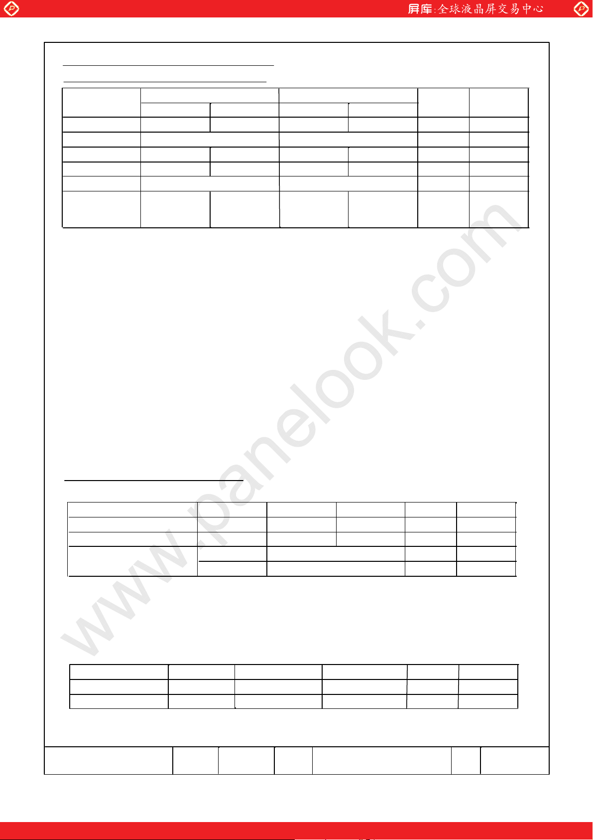
1. ABSOLUTE MAXIMUM RATINGS
1.1 Environmental Absolute Maximum Ratings
Operating
ITEM
Temperature
Humidity
Vibration
Shock
Corrosive Gas
Min. Max. Min. Max.
0 -20
50 60
2)
-
-
4.9(0.5G) 9.8 (1G)
29.4(3G) 147 (15G)
ot Acceptable
Illumination at
LCD Surface
--
50,000 50,000
ote 1) Temperature and Humidity should be applied to the glass surface of a Super-TFT module,
not to the system installed with a module.
The temperature at the center of rear surface should be less than 70℃ on the condition of operating.
The brightness of a CCFL tends to drop at low temperature. Besides, the life-time becomes shorter
at low temperature.
2) Ta≦40
℃‥‥‥
Relative humidity should be less than
85%RH max. Dew is prohibited.
Storage
2)
-
-
ot Acceptable
Unit
%
m/s
m/s
℃
RH
2
2
-
lx
1),5
1
3
4
T a> 40
℃‥‥‥
3) Frequency of the vibration is between 15Hz and 100Hz. (Remove the resonance point)
4) Pulse width of the shock is 10 ms.
5) Long operation under low temperature may cause some portion of display area to be reddish for
several minutes after turning on the product.
However, it does not affect the characteristics and reliability of the product.
Relative humidity should be lower than
the moisture of the 85%RH at 40℃.
1.2 Electrical Absolute Maximum Ratings
(1)Super-TFT Module
ITEM SYMBOL Min. Max. Unit
Power Supply Voltage
Input Voltage for logic
Electrostatic Durability
1)It is applied to pixel data signal and clock signal.
2)Discharge Coefficient:200pF-250Ω, Environmental:25℃-70%RH
3)It is applied to I/F connector pins.
4)It is applied to the surface of a metallic bezel and a LCD panel.
V
V
V
V
ESD0
ESD1
DD
0 13.2 V
-0.3 3.6 V
100
±
8
±
k
Vss = 0 V
1
V
V
2),3
2),4
(2) Back-light
ITEM
Input Current
Input Voltage
SYMBOL
IL
VL
Min. Max.
-
-
7.0
2,000
Unit
mArms
Vrms
ote 1)The specification shall be applied to each CFL. The specification is defined at ground line.
2)The specification shall be applied at connector pins for a CFL at start-up.
Date
One step solution for LCD / PDP / OLED panel application: Datasheet, inventory and accessory!
No
.10,2003 3284STD-2188-1
Sheet
No.
GND = 0 V
1
PageHitachi Displays, Ltd.
4-1/1
www.panelook.com
Page 5
Global LCD Panel Exchange Center
v
N
NOTE
)
)
)
χ
χ
)
)
)
]
2. OPTICAL CHARACTERISTICS
The following optical characteristics are measured under stable conditions. It takes about 30 minutes
to reach stable conditions. The measuring point is the center of display area unless otherwise noted.
The optical characteristics should be measured in a dark room or equivalent state.
Measuring equipment:Pritchard 1980A, or equivalent
Temperature =25
IL=5.0mA (average of 16 pieces of CFLs, PWM:Duty 100%) , CTL = Low
℃、
www.panelook.com
VDD=12.0V、f V=60Hz
、
ITEM
Contrast Ratio
Response
Time
Brightness of white Bwh
Brightness uniformity
Color
Chromaticity
CIE
(
)
Variation of
Color Position
(CIE)
Rise ton
Fall
Red
Green
Blue
White
Red
Green
Blue
White
SYMBOL CONDITIO
Min.
CR
300
--
toff
Buni %
χ
y
χ
y
χ
y
χ
y
Δ
Δy
Δχ
Δy
Δ
Δy
Δχ
Δy
θ
φ
180
θ=
1
=+50 °
°
=0
,
°
,
1
0
90°
270°
°
-
-
0.61
0.29
0.26
0.58
0.12
0.04
0.245
0.252
- 0.04
-
-
-
-
-
-
-
Typ.
500
-
470
-
0.64
0.32
0.29
0.61
0.15
0.07
0.275
0.282
-
-
-
-
-
-
-
-
Max. UNIT
-
30
30
-
40
0.67
0.35
0.32
0.64
0.18
0.10
0.335
0.342
0.04
0.04
0.04
0.04
0.04
0.04
0.04
-
ms 3
ms
cd/m300
-
2
-
2
, CTL:High
3) , CTL:High
4
[Gray scale
=255]
5
[Gray scale
=255
Contrast Ratio at 85 ° CR85 °
Date
One step solution for LCD / PDP / OLED panel application: Datasheet, inventory and accessory!
No
.10,2003 3284STD-2188-1
Sheet
No.
10
--
-
PageHitachi Displays, Ltd.
5-1/2
www.panelook.com
Page 6
Global LCD Panel Exchange Center
v
N
%
(1)
(2)
(3)
(4)
(5)
(6)
(7)
(8)
(9)
%50%90%
%50%90%
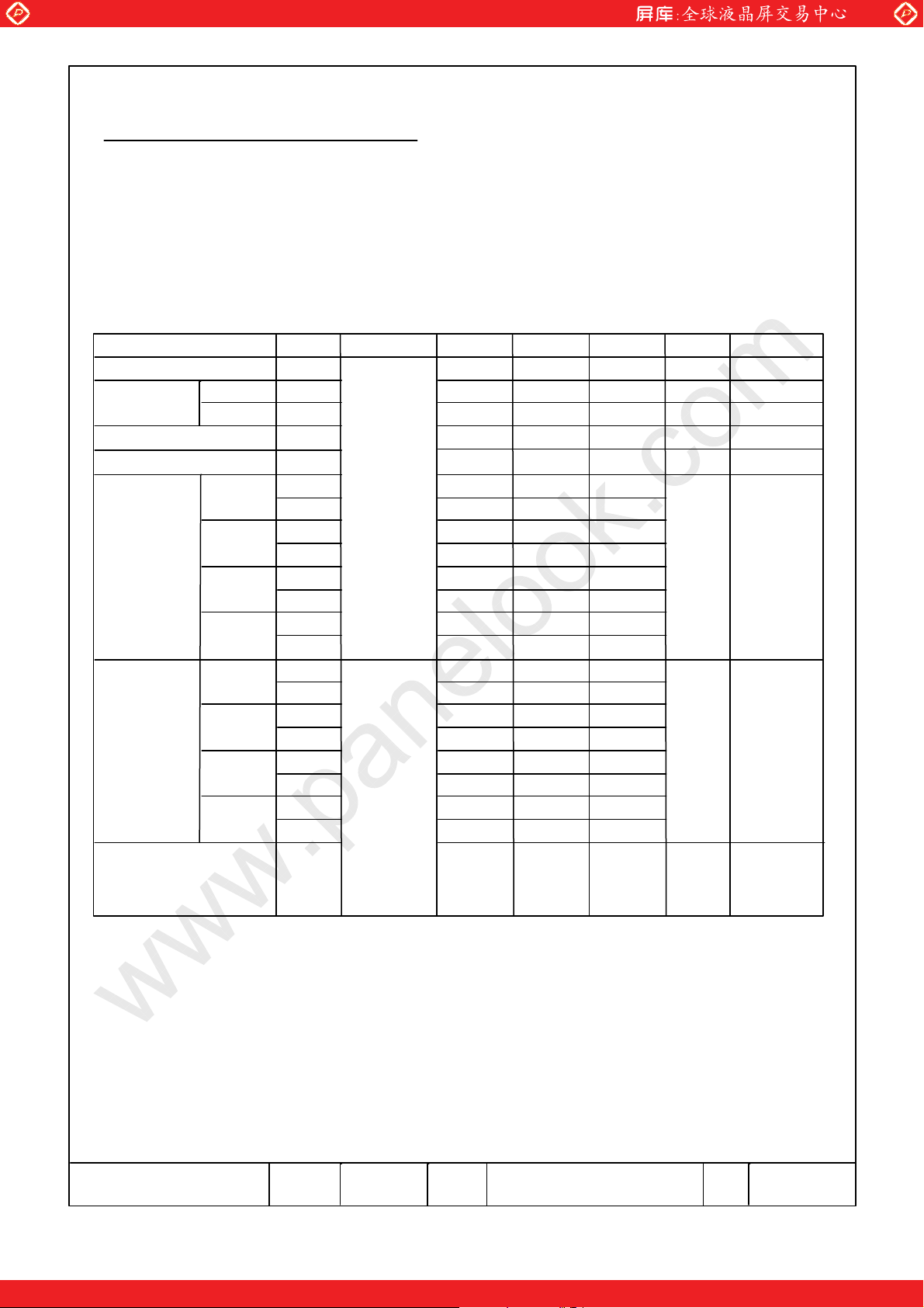
ote 1) Definition of Viewing Angle
12 o'clock
(
)
φ
Y
=90°
www.panelook.com
=0 °
θ
Z
θ
eye
=180°
φ
9 o'clock
(
X'
)
Super-TFT Module
2) Definition of Contrast Ratio (CR)
(Luminance at displaying WHITE)
=
CR
(Luminance at displaying BLACK)
3) Definition of Response Time
Displaying
Data Signal
Optical
BLACK
100
90
Response
( Luminance)
10
0
ton
WHITE
Y'Z'
φ
6 o'clock
(
φ
=270°
)
toff
φ
X(3 o'clock
BLACK
=0 °
)
4) Definition of Brightness Uniformity
Display pattern is white (255 level) . The brightness
10
uniformity is defined as the following equation. Brightness at each
point is measured, and average, maximum and minimum
brightness is calculated.
Bmax or Bmin−Bave
10
measuring points
:
Buni=
Bave
where, Bmax = Maximum brightness
×100
Bmin = Minimum brightness
Bave= Average brightness =
5)Variation of color position on CIE is defined as difference between colors at θ=0°and
at
50°&φ=0 °,90°,180°,270°.
θ=
Date
No
.10,2003 3284STD-2188-1
Sheet
No.
9
(B(k))
Σ
k=1
9
PageHitachi Displays, Ltd.
5-2/2
One step solution for LCD / PDP / OLED panel application: Datasheet, inventory and accessory!
www.panelook.com
Page 7
Global LCD Panel Exchange Center
v
Note
V
V
A1),2)
V
R
V
Note
z
V
N
N
3. ELECTRICAL CHARACTERISTICS
3.1 TFT-LCD Module
ITEM
Power Supply Voltage
Power Supply Current
Ripple Voltage of Power Supply
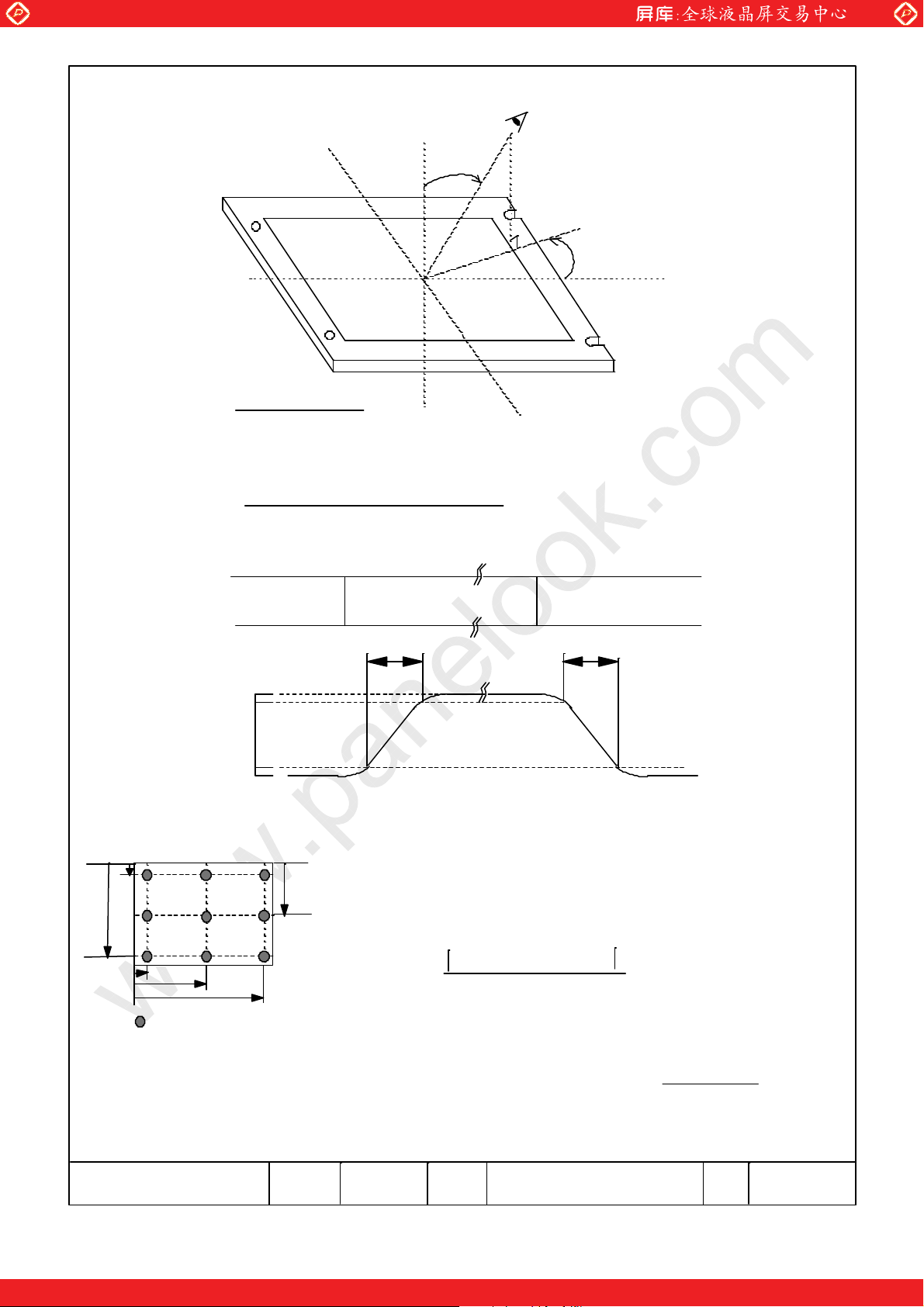
ote 1) DC current at fv=60.0Hz, fCLK=82MHz, VDD=12.0V and Display pattern is white.
DC Ampere Meter
www.panelook.com
SYMBOL Min.
11.4
−
−
Super-TFT Module
V
V
I
DD
DD
DD
Typ. Max.
12.0
0.59
−
DD
SS
Ta=25℃,Vss=0V
Unit
12.6
0.80
0.15
2) Current fuse is built in a module. Current capacity of power supply for VDD
should be larger than 4A, so that the fuse can be opened at the trouble of power supply.
3.2 Back Light
ITEM
Input Current
Input Voltage VL Vrms
Frequency
Kick-Off Voltage
SYMBOL Min.
IL
3.0
--
f0
Vs
50
-
Typ. Max.
5.0
6.0
1290
55
-
60
1,600
Unit
mArms
kH
1)
2)
3)
otes 1) The specification shall be applied to each CFL. The specification is defined at ground line.
2) Frequency of power supply for a CFL may cause the interference with HSYNC frequency
and cause beat or flicker on the display. Therefore, lamp frequency shall be as different
as possible from HSYNC frequency in order to avoid the interference.
3) Ta = 0 degree
Date
One step solution for LCD / PDP / OLED panel application: Datasheet, inventory and accessory!
No
.10,2003 3284STD-2188-1
Sheet
No.
PageHitachi Displays, Ltd.
6-1/1
www.panelook.com
Page 8

Global LCD Panel Exchange Center
v
pply
g
)
S
4. BLOCK DIAGRAM
(1) Super-TFT Module
www.panelook.com
Drain Driver
LVD
(Display data
and timin
DC power
su
signal
(2) Back light unit
HV16
CN2
HV15
HV14
CN3
HV13
HV12
CN4
HV11
CN1
LVDS
Receiver
Timing
Converter
DC/DC
Converter
Lamp 16
Lamp 15
Lamp 14
Lamp 13
Lamp 12
Lamp 11
D1 D2 D3840
G1
G2
Super TFT-LCD
G768
LV16
LV15
LV14
LV13
CN10
LV12
LV11
CN5
CN6
CN7
CN8
CN9
HV10
HV9
HV8
HV7
HV6
HV5
HV4
HV3
HV2
HV1
Date
Lamp 10
Lamp 9
Lamp 8
Lamp 7
Lamp 6
Lamp 5
Lamp 4
Lamp 3
Lamp 2
Lamp 1
No
.10,2003 3284STD-2188-1 7-1/1
Sheet
No.
LV10
LV9
LV8
LV7
LV6
LV5
LV4
LV3
LV2
LV1
PageHitachi Displays, Ltd.
CN11
One step solution for LCD / PDP / OLED panel application: Datasheet, inventory and accessory!
www.panelook.com
Page 9

Global LCD Panel Exchange Center
v
S
)
)
a
)
S
)
)
S
)
)
S
)
)
k
)
S
)
)
a
)
S
)
)
L
)
N
)
N
p
p
p
p
5. INTERFACE PIN ASSIGNMENT
5. 1 TFT-LCD MODULE
CN1 : JAE FI-SEB20P-HF13
(Matching connector : JAE FI-SE20M or equivalent)
Pin No. Symbol Description Note
1 VDD Power Supply (typ.+12V) 1)
2 VDD
3 VS
4 VSS
5 Rx0- Pixel Dat
6 Rx0+
7 VS
8 Rx1- Pixel Data 3)
9 Rx1+
10 VS
11 Rx2- Pixel Data 3)
12 Rx2+
13 VS
14 CLK- Pixel Cloc
15 CLK+
16 VS
17 Rx3- Pixel Dat
18 Rx3+
19 VS
20 CT
otes 1) All VDD pins shall be connected to +12.0V(Typ.).
2) All VSS pins shall be grounded. Metal bezel is internally connected to VSS.
3) Rx n+ and Rx n- (n=1,2,3) should be wired by twist-pairs or side-by-side FPC patterns, respectively.
4) Low level : 0〜0.15V, High level : 2.5〜5.0V
www.panelook.com
GND (0V
GND (0V
GND (0V
GND (0V
GND (0V
GND (0V
Low:A line trace ON , High:A line trace OFF 4
2
3
2
2
2
3
2
3
2
5. 2 BACK-LIGHT UNIT
CN2,CN3,CN4,CN5,CN6,CN7,CN8,CN9 : JST BHR-03VS-1
(Matching connector : JST SM02 (0.8) B-BHS-1-TB or equivalent)
FunctionSYMBOLPin No.
1
2
3
HV-2(n-10)
NC
HV-2(n-10)-1
ote 1) n=CN Number
CN10,CN11
: JST ZHR-8
CN11 CN10
Pin No.
1
2
3
4
5
6
7
8
LV1
LV2
LV3
LV4
LV5
LV6
LV7
LV8
Power Supply for Lamp Even side(High Voltage)
Power Supply for Lamp Odd side(High Voltage
FUNCTIONSYMBOL
Lamp1 LV
2 LV
Lam
Lamp3 LV
Lamp4 LV
Lamp5 LV
6 LV
Lam
Lamp7 LV
Lamp8 LV
Pin No.
FUNCTIONSYMBOL
1
2
3
4
5
6
7
8
LV9
LV10
LV11
LV12
LV13
LV14
LV15
LV16
Lamp9 LV
10 LV
Lam
Lamp11 LV
Lamp12 LV
Lamp13 LV
14 LV
Lam
Lamp15 LV
Lamp16 LV
Date
One step solution for LCD / PDP / OLED panel application: Datasheet, inventory and accessory!
No
.10,2003 3284STD-2188-1
Sheet
No.
PageHitachi Displays, Ltd.
8-1/5
www.panelook.com
Page 10

Global LCD Panel Exchange Center
v
r
play
(
)
(
)
y
N
y
+
R
T
BLOCK DIAGRAM OF INTERFACE
TV setSide
www.panelook.com
CN1
TFT-LCD ModuleSide
R0-R7
G0-G7
B0-B7
Hsync
Vsync
DTMG
Host
Graphics
Controller
R0〜R7
G0〜G7
B0〜B7
HSYNC
VSYNC
DTMG
TxIN
Rx 0+
Rx 0-
Rx 1+
Rx 1-
Rx 2+
Rx 2-
Rx 3+
Rx 3-
CLK
CLK-
LVDS Transmitter LVDS Receive
THC63LVDM83A
LVDF83A
Pixel R Data
:
Pixel G Data
:
Pixel B Data
:
Horizontal synchronization signal
:
Vertical synchronization signal
:
Dis
:
timing signal
100Ω
100Ω
100Ω
100Ω
100Ω
THC63LVDF84A
THC63LVDF84B
xOU
R0‐R7
G0‐G7
B0‐B7
nc
Hs
Vsync
DTMG
PLLPLL
DCLK
Timing
Converter
otes 1) The system must have the transmitter to drive the module.
2) LVDS cable impedance shall be 50 ohms per signal line or about 100 ohms per twist-pair line when it is used
differentiall
.
Date
No
.10,2003 3284STD-2188-1 8-2/5
Sheet
No.
PageHitachi Displays, Ltd.
One step solution for LCD / PDP / OLED panel application: Datasheet, inventory and accessory!
www.panelook.com
Page 11

Global LCD Panel Exchange Center
v
N
A
O
R
C
C
D
0
2
4
6
7
8
9
5
)
K
+
K
-
LVDS INTERFACE
TR
SIGNAL TH
R2 51 Tx IN0 27 Rx OUT
R3 52 Tx IN1 29 Rx OUT1 R3
R4 54 Tx IN2 TA OUT0+ Rx 0+ 30 Rx OUT
R5 55 Tx IN3 32 Rx OUT3 R5
R6 56 Tx IN4 33 Rx OUT
R7 3 Tx IN6 TA OUT0- Rx 0- 35 Rx OUT
G2 4 Tx IN7 37 Rx OUT
G3 6 Tx IN8 38 Rx OUT
G4 7 Tx IN9 39 Rx OUT
G5 11 Tx IN12 TA OUT1+ Rx 1+ 43 Rx OUT12 G5
G6 12 Tx IN13 45 Rx OUT13 G6
G7 14 Tx IN14 46 Rx OUT14 G7
B2 15 Tx IN15 TA OUT1- Rx 1- 47 Rx OUT15 B2
24bit B3 19 Tx IN18 51 Rx OUT18 B3
B4 20 Tx IN19 53 Rx OUT19 B4
B5 22 Tx IN20 54 Rx OUT20 B5
B6 23 Tx IN21 TA OUT2+ Rx 2+ 55 Rx OUT21 B6
B7 24 Tx IN22 1 Rx OUT22 B7
HSYNC 27 Tx IN24 3 Rx OUT24 HSYNC
VSYNC 28 Tx IN25 TA OUT2- Rx 2- 5 Rx OUT25 VSYNC
DTMG 30 Tx IN26 6 Rx OUT26 DTMG
R0 50 Tx IN27 7 Rx OUT27 R0
R1 2 Tx IN5 34 Rx OUT
G0 8 Tx IN10 TA OUT3+ Rx 3+ 41 Rx OUT10 G0
G1 10 Tx IN11 42 Rx OUT11 G1
B0 16 Tx IN16 49 Rx OUT16 B0
B1 18 Tx IN17 TA OUT3- Rx 3- 50 Rx OUT17 B1
RSVD 1
DCL
TRANSMITTER INTERFACE C
THC63LVDM83A TH
PIN INPUT PC TFT-LC
25 Tx IN23 2 Rx OUT23 not connect
31 TxCLK IN TxCLK OUT
www.panelook.com
ACE CONNECTOR REC RECEIVE
TxCLK OUT
RxCLK IN+ 26 RxCLK OUT DCL
RxCLK IN-
THC63LVDF84A CONTROL
TFT
PIN OUTPUT INPUT
R2
R4
R6
R7
G2
G3
G4
R1
R0〜R7
G0〜G7
B0〜B7
HSYNC
VSYNC
DTMG
Pixel R Data(7;MSB, 0;LSB
:
Pixel G Data (7;MSB, 0;LSB
:
Pixel B Data (7;MSB, 0;LSB
:
Horizontal synchronization signal
:
Vertical synchronization signal
:
Display timing signal
:
otes 1) RSVD(reserved) pins on the transmitter shall be "H" or "L".
)
)
)
Date
One step solution for LCD / PDP / OLED panel application: Datasheet, inventory and accessory!
No
.10,2003 3284STD-2188-1
Sheet
No.
PageHitachi Displays, Ltd.
8-3/5
www.panelook.com
Page 12
Global LCD Panel Exchange Center
v
a
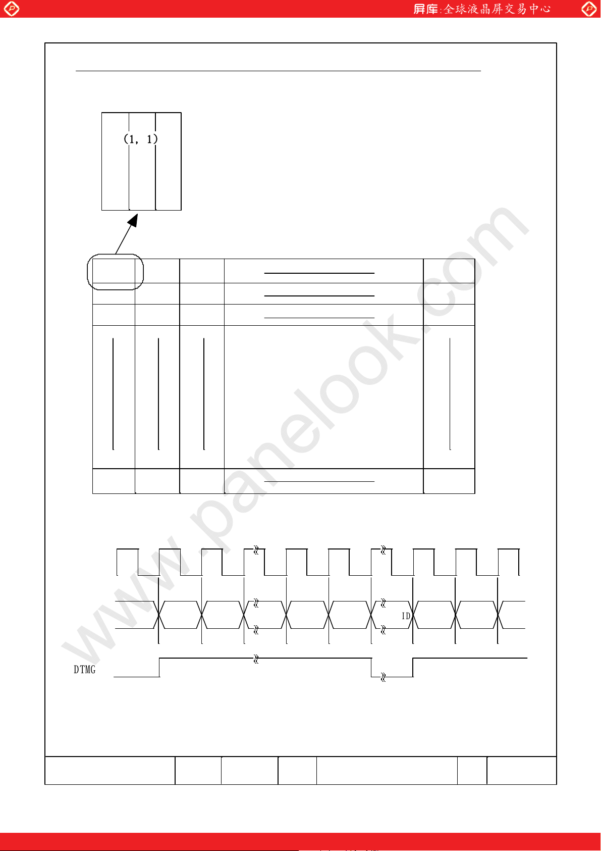
CORRESPONDENCE BETWEEN INPUT DATA AND DISPLAY IMAGE
Display data of adjacent one pixel is latched during one cycle of DCLK.
www.panelook.com
ʢøɼøʣ
pixel:R0〜R7 :R data
G0〜G7 :G data
B0〜B7 :B dat
ęĎĉ
1,1 1,2 1,3 1,1280
2,1 2,2 2,3 2,1280
3,1 3,2 3,3 3,1280
DCLK
R0〜R7
G0〜G7
B0〜B7
DTMG
768,1 768,2 768,3
INVALID
1,1 1,2 1,1279 1,1280 2,1 2,2
Date
INVALID
No
.10,2003 3284STD-2188-1
Sheet
No.
768,1280
PageHitachi Displays, Ltd.
8-4/5
One step solution for LCD / PDP / OLED panel application: Datasheet, inventory and accessory!
www.panelook.com
Page 13

Global LCD Panel Exchange Center
v
t
D
a
N
RELATIONSHIP BETWEEN DISPLAY COLORS AND INPUT SIGNALS
RedRedDa
Input R7 R6 R5 R4 R3 R2 R1 R0 G7 G6 G5 G4 G3 G2 G1 G0 B7 B6 B5 B4 B3 B2 B1 B0
Color
Black 0 0 0 0 0 0 0 0 0 0 0 0 0 0 0 0 0 0 0 0 0 0 0 0
Red(255) 1 1 1 1 1 1 1 1 0 0 0 0 0 0 0 0 0 0 0 0 0 0 0 0
Green(255) 0 0 0 0 0 0 0 0 1 1 1 1 1 1 1 1 0 0 0 0 0 0 0 0
Basic Blue(255) 0 0 0 0 0 0 0 0 0 0 0 0 0 0 0 0 1 1 1 1 1 1 1 1
Color Cyan 0 0 0 0 0 0 0 0 1 1 1 1 1 1 1 1 1 1 1 1 1 1 1 1
Magenta 1 1 1 1 1 1 1 1 0 0 0 0 0 0 0 0 1 1 1 1 1 1 1 1
Yellow 1 1 1 1 1 1 1 1 1 1 1 1 1 1 1 1 0 0 0 0 0 0 0 0
White 1 1 1 1 1 1 1 1 1 1 1 1 1 1 1 1 1 1 1 1 1 1 1 1
Black 0 0 0 0 0 0 0 0 0 0 0 0 0 0 0 0 0 0 0 0 0 0 0 0
Red(1) 0 0 0 0 0 0 0 1 0 0 0 0 0 0 0 0 0 0 0 0 0 0 0 0
Red(2) 0 0 0 0 0 0 1 0 0 0 0 0 0 0 0 0 0 0 0 0 0 0 0 0
Red : : : : : : : : : : : : : : : : : : : : : : : : :
: : : : : : : : : : : : : : : : : : : : : : : : :
Red(254) 1 1 1 1 1 1 1 0 0 0 0 0 0 0 0 0 0 0 0 0 0 0 0 0
Red(255) 1 1 1 1 1 1 1 1 0 0 0 0 0 0 0 0 0 0 0 0 0 0 0 0
Black 0 0 0 0 0 0 0 0 0 0 0 0 0 0 0 0 0 0 0 0 0 0 0 0
Green(1) 0 0 0 0 0 0 0 0 0 0 0 0 0 0 0 1 0 0 0 0 0 0 0 0
Green(2) 0 0 0 0 0 0 0 0 0 0 0 0 0 0 1 0 0 0 0 0 0 0 0 0
Green : : : : : : : : : : : : : : : : : : : : : : : : :
: : : : : : : : : : : : : : : : : : : : : : : : :
Green(254) 0 0 0 0 0 0 0 0 1 1 1 1 1 1 1 0 0 0 0 0 0 0 0 0
Green(255) 0 0 0 0 0 0 0 0 1 1 1 1 1 1 1 1 0 0 0 0 0 0 0 0
Black 0 0 0 0 0 0 0 0 0 0 0 0 0 0 0 0 0 0 0 0 0 0 0 0
Blue(1) 0 0 0 0 0 0 0 0 0 0 0 0 0 0 0 0 0 0 0 0 0 0 0 1
Blue(2) 0 0 0 0 0 0 0 0 0 0 0 0 0 0 0 0 0 0 0 0 0 0 1 0
Blue : : : : : : : : : : : : : : : : : : : : : : : : :
: : : : : : : : : : : : : : : : : : : : : : : : :
Blue(254) 0 0 0 0 0 0 0 0 0 0 0 0 0 0 0 0 1 1 1 1 1 1 1 0
Blue(255) 0 0 0 0 0 0 0 0 0 0 0 0 0 0 0 0 1 1 1 1 1 1 11
MSB LSB MSB LSB MSB LSB
www.panelook.com
edData GreGreen
reenDataData BluBlueD
lueData
otes 1) Definition of gray scale:
Color(n)
・・・・
2) Data: 1:High, 0:Low
Number in parenthesis indicates gray scale level. Larger n corresponds to brighter level.
Date
No
.10,2003 3284STD-2188-1
Sheet
No.
PageHitachi Displays, Ltd.
8-5/5
One step solution for LCD / PDP / OLED panel application: Datasheet, inventory and accessory!
www.panelook.com
Page 14

Global LCD Panel Exchange Center
v
N
,
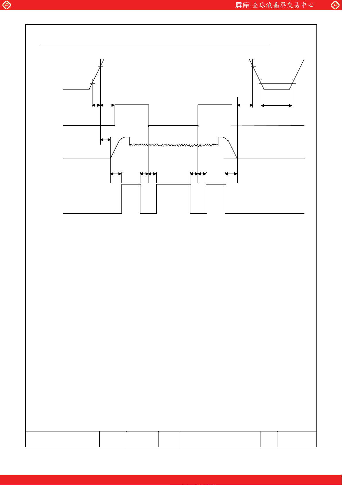
6. INTERFACE TIMING
6.1 TIMING CHART
www.panelook.com
DCLK
HSYNC
VSYNC
HSYNC
DTMG
VSYNC
TCIP
TWH
TWV
TCIL
0.8V
TSV
THBP THFP
THV
THP
TWD
TVP
TVBP TVFP
DTMG
TSTC
1.5V
THTC
1.5V
DCLK
VSYNC,HSYNC,DTMG,
R0〜7
G0〜7,B0〜7
1.5V
otes 1) Reference level for each timing signal is 1.5V unless it is stated on the chart , high level voltage(VIH) and
low level voltage(VIL) are defined as follows:
VIH≧
2.0
V VIL≦
0.8
V
The above definition conforms to the specifications of LVDS transmitter
( THC63LVDM83A / by THine Microsystems, Inc.).
2) The timing of DCLK to other signals conforms to the specifications of LVDS transmitter.
3) HSYNC, VSYNC timing is specified in negative polarity.
4) HSYNC pulse is needed while data is invalid (blanking period).
Date
One step solution for LCD / PDP / OLED panel application: Datasheet, inventory and accessory!
No
.10,2003 3284STD-2188-1
Sheet
No.
PageHitachi Displays, Ltd.
9-1/3
www.panelook.com
Page 15

Global LCD Panel Exchange Center
v
y
V
h
)
)
C
)
)
y
V
h
)
)
C
)
)
g
6.2 INTERFACE TIMING SPECIFICATIONS
6.2.1 CTL=Low
DCLK Frequenc
HSYNC Frequency fH 44.8 49.7 53.6 kHz
VSYNC Frequency fV 58 60 62 Hz 4)
DTMG Horizontal Back porch THBP 16 - - TCIP
COMMON Set up Time TST
Item Symbol Min. Typ. Max. Unit Note
Duty D 0.35 0.5 0.65 - D=TCIL/TCIP
Period THP 1646 - 1708 TCIP
Width-Active TWH 8 - 240 TCIP
Set up Time TS
Hold Time THV 8 - - TCIP
Period TVP 772 - 900 THP
Width-Active TWV 1 - 120 THP
Horizontal Front Porch THFP 0 - - TCIP
Vertical Back Porc
Vertical Front porch TVFP 2 - 1
Width-Active TWD 1280 1280 1280 TCIP
Hold Time THTC 3 - 2
www.panelook.com
fCLK 73.7 82 82.6 MHz
0 - - TCIP to HSYNC
TVBP 2 - 1
5 - 2
THP
THP
ns
ns
6.2.2 CTL=Hi
DCLK Frequenc
HSYNC Frequency fH 41 49.7 53.6 kHz
VSYNC Frequency fV 48 60 62 Hz 4)
DTMG Horizontal Back porch THBP 16 - - TCIP
COMMON Set up Time TST
In addition to the above, these timing should conforms to the followings.
h
Item Symbol Min. Typ. Max. Unit Note
fCLK 73.7 82 82.6 MHz
Duty D 0.35 0.5 0.65 - D=TCIL/TCIP
Period THP 1646 - 2000 TCIP
Width-Active TWH 8 - 240 TCIP
Set up Time TS
Hold Time THV 8 - - TCIP
Period TVP 772 - 900 THP
Width-Active TWV 1 - 120 THP
Horizontal Front Porch THFP 0 - - TCIP
Vertical Back Porc
Vertical Front porch TVFP 2 - 1
Width-Active TWD 1280 1280 1280 TCIP
Hold Time THTC 3 - 2
TVBP 2 - 1
0 - - TCIP to HSYNC
THP
THP
5 - 2
ns
ns
1) TVBP+TVFP≧4 THP
2) TSTC and THTC conforms to the specifications of LVDS transmitter.
It is preferable to check the specifications of LVDS transmitter in your system.
3) TVP fluctuation should be kept within ±1 line.
4) A line trace function does not allowed in PAL.
Date
One step solution for LCD / PDP / OLED panel application: Datasheet, inventory and accessory!
No
.10,2003 3284STD-2188-1
Sheet
No.
PageHitachi Displays, Ltd.
9-2/3
www.panelook.com
Page 16
Global LCD Panel Exchange Center
v
V
V
RTCR
R
V
R
R
R
V
V
V
V
6.3 TIMING BETWEEN INTERFACE SIGNALS AND POWER SUPPLY
12
10
www.panelook.com
10
DD
V
CTL
VI
BL
0
High
Low
ON
OFF
1
TP
A line trace OFF
TD
TB
A line trace ON
alid
TBCF TBC
A line trace OFF
TBCF TBC
TDF TIN
TBF
Timing of power supply voltage and input signals should be used under
the following specifications.
1
0ms≦ TPR ≦ 10ms
10ms≦ TDR ≦ 50ms
0ms≦TDF≦50ms
TIN≧ 1s
200ms≦TBR≦500ms
TBF≦100ms
4ms≦TCR≦10ms
0ms≦T BCF
200 ms≦TBCR
During CTL switching, follows timing should be kept.
1646≦THP≦2046
・
Don't continuously output timing TVP≦79 or TVP≧2047
・
Don't change DCLK frequency.
・
Date
One step solution for LCD / PDP / OLED panel application: Datasheet, inventory and accessory!
No
.10,2003 3284STD-2188-1
Sheet
No.
PageHitachi Displays, Ltd.
9-3/3
www.panelook.com
Page 17

Page 18

Page 19

Global LCD Panel Exchange Center
v
N
高電圧注意
高電圧注意
8. DESIGNATION OF LOT MARK
8.1 LOT MARK
Month 2)
Year 1)
Week 3)
www.panelook.com
5 digits for production number
00001〜99999
(
Special mark 4)
Production management sign
)
otes
1)
2003
2004
2005
2006
Year Mark
3
4
5
6
2
)
Month
1
2
3
4
5
6
Mark
01
02
03
04
05
06
Month Mark
7
8
9
10
11
12
07
08
09
10
11
12
3)
Week(Day
1〜7
8〜14
15〜21
22〜28
)
29〜31
4) It is the mark that was opened up by production person to take
correspondence with production number.
8.2 Revision (REV.) control
REV. is the column for manufacturing convenience. A-Z except I and O may be written
on this column.
8.3 Location of lot mark
Lot mark is printed on a label. The label is on the metallic bezel as shown in 7. External Dimensional.
The style of character will be changed without notice.
Mark
1
2
3
4
5
ďĐěĈĊďĐ
TFTMD80120CBB
3041H00001
Lot mark
本ディスプレイユニット内の蛍光管には水銀が含まれております。液晶ディスプレイの廃棄
に当たっては地方自治体の条例または規則に従って廃棄して下さい。
COLDCATHODEFLUORESCENT LAMPINCOLOR LCDCONTAINSMERCURY.
PLEASEFOLLOWLOCALORDINANCESORREGULATIONSFORITSDISPOSAL.
MADEIN JAPAN .
(a) Made in Japan
One step solution for LCD / PDP / OLED panel application: Datasheet, inventory and accessory!
CAUTIONHIGHVOLTAGE
M000000F05400001
Date
No
.10,2003 3284STD-2188-1
Sheet
No.
ďĐěĈĊďĐ
TFTMD80120CBB
3041S00001
MADEINTAIWAN R.O.C.
本ディスプレイユニット内の蛍光管には水銀が含まれております。液晶ディスプレイの廃棄
に当たっては地方自治体の条例または規則に従って廃棄して下さい。
COLDCATHODEFLUORESCENT LAMPINCOLOR LCDCONTAINSMERCURY.
PLEASEFOLLOWLOCALORDINANCESORREGULATIONSFORITSDISPOSAL.
(b) Made in Taiwan R.O.C.
CAUTIONHIGHVOLTAGE
R000000F05400001
PageHitachi Displays, Ltd.
11-1/1
www.panelook.com
Page 20
Global LCD Panel Exchange Center
v
e
e
n
10. PRECAUTION
Please pay attention to the followings when a Super-TFT module with a back-light unit is used,
handled and mounted.
10.1 Precaution to handling and mounting
(1) Applying strong force to a part of the module may cause partial deformation of frame or mold,
and cause damage to the display.
(2) The module should gently and firmly be held by both hands. Never hold by just one hand in order
to avoid any internal damage. Never drop or hit the module.
(3) The module should be installed with mounting holes at each corner of a module.
(4) Uneven force such as twisted stress should not be applied to a module when a module is mounted
on the cover case. The cover case must have sufficient strength so that external force can not be
transmitted directly to a module.
(5) It is recommended to leave a space between a module and a holding board of a module so that
partial force is not applied to a module.
www.panelook.com
Effective display area
Polarizer
Super-TFT modul
above precautio
(5)
Cover case
B-zone
Edge of
cover cas
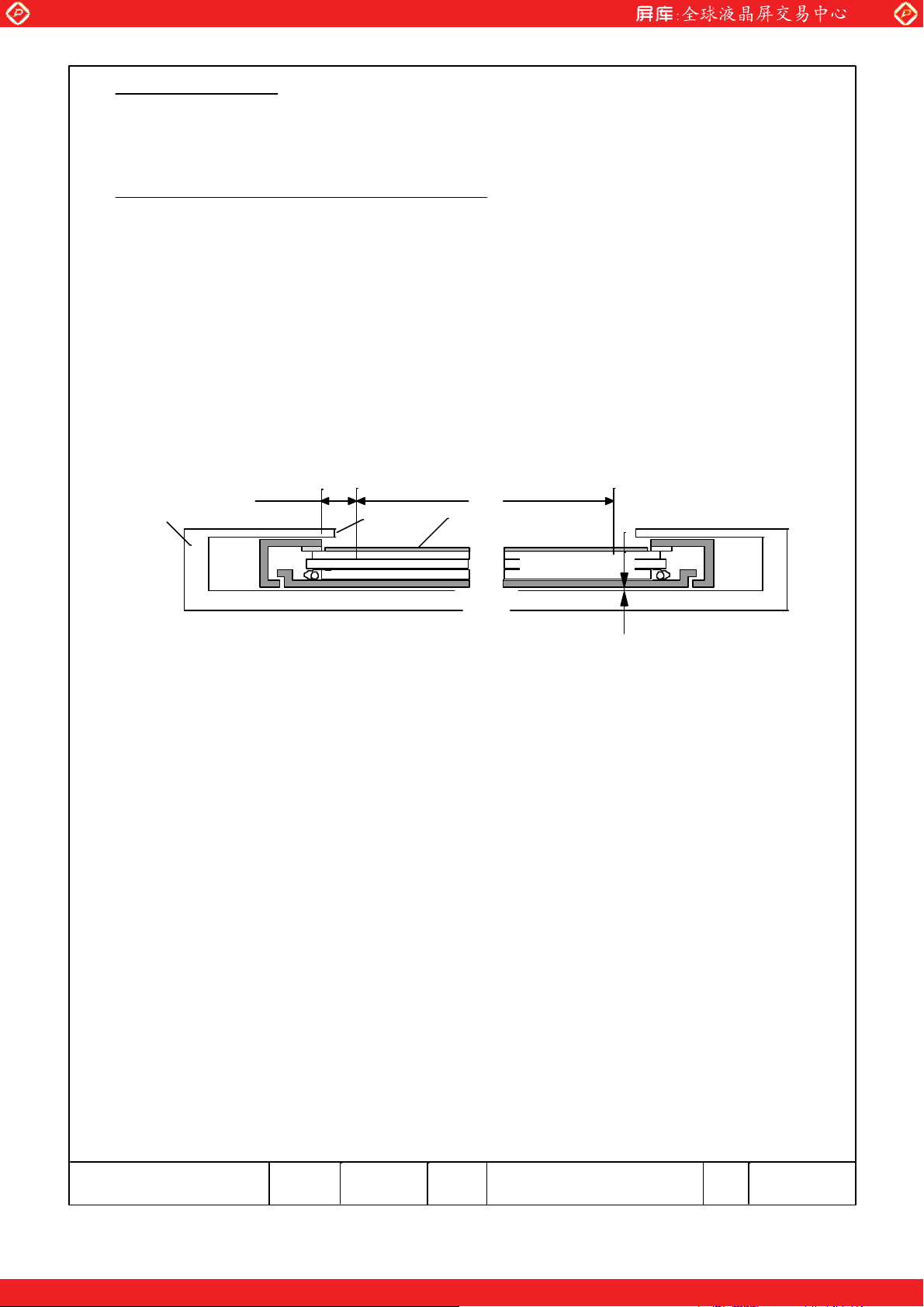
Fig.1 Cross sectional view of a monitor set
(6) The edge of a cover case should be located inside more than 1mm from the edge of a module front
frame.
(7) A transparent protective plate should be added on the display area of a module in order to protect
a polarizer and Super-TFT cell. The transparent protective plate should have sufficient strength
so that the plate can not touch a module by external force.
(8) Materials included acetic acid and choline should not be used for a cover case as well as other parts
and boards near a module. Acetic acid attacks a polarizer. Choline attacks electric circuits due to
electro-chemical reaction.
(9) The polarizer on a TFT cell should carefully be handled due to its softness, and should not be touched,
pushed or rubbed with glass, tweezers or anything harder than HB pencil lead. The surface of
a polarizer should not be touched and rubbed with bare hand, greasy clothes or dusty clothes.
(10) The surface of a polarizer should be gently wiped with absorbent cotton, chamois or other soft
materials slightly contained petroleum benzene when the surface becomes dirty. Normal-hexane
as cleaning chemicals is recommended in order to clean adhesives which fix front/rear polarizers
on a Super-TFT cell. Other cleaning chemicals such as acetone, toluen and alcohol should not be
used to clean adhesives because they cause chemical damage to a polarizer.
(11) Saliva or water drops should be immediately wiped off. Otherwise, the portion of a polarizer may
be deformed and its color may be faded.
(12) The module should not be opened or modified. It may cause not to operate properly.
Date
One step solution for LCD / PDP / OLED panel application: Datasheet, inventory and accessory!
No
.10,2003 3284STD-2188-1
Sheet
No.
PageHitachi Displays, Ltd.
12-1/3
www.panelook.com
Page 21

Global LCD Panel Exchange Center
v
(13) Metallic bezel of a module should not be handled with bare hand or dirty gloves. Otherwise,
color of a metallic frame may become dirty during its storage. It is recommended to use clean
soft gloves and clean finger stalls when a module is handled at incoming inspection process and
production (assembly) process.
(14) Lamp(CCFL) cables should not be pulled and held.
10.2 Precaution to operation
(1) The ambient temperature near the operated module should be satisfied with the absolute maximum
ratings. Unless it meets the specifications, sufficient cooling system should be adopted to system.
(2) The spike noise causes the mis-operation of a module. The level of spike noise should be as follows:
-200mV<=over- and under- shoot of VDD <= +200mV
VDD including over- and under- shoot should be satisfied with the absolute maximum ratings.
(3) Optical response time, luminance and chromaticity depend on the temperature of a Super-TFT
module. Response time and saturation time of CCFL luminance become longer at lower temperature
operation.
(4) Sudden temperature change may cause dew on and/or in the a module. Dew males damage to a
polarizer and/or electrical contacting portion. Dew causes fading of displayed quality.
(5) Fixed patterns displayed on a module for a long time may cause after-image. It will be recovered
soon.
(6) A module has high frequency circuits. Sufficient suppression to electromagnetic interference should
be done by system manufacturers. Grounding and shielding methods may be effective to minimize
the interference.
(7) Noise may be heard when a back-light is operated. If necessary, sufficient suppression should be
done by system manufacturers.
(8) The module should not be connected or removed while a main system works.
(9) Inserting or pulling I/F connectors causes any trouble when power supply and signal dates are
on-state.I/F connectors should be inserted and pulled after power supply and signal dates are
turned off.
www.panelook.com
10.3 Electrostatic discharge control
(1) Since a module consists of a Super-TFT cell and electronic circuits with CMOS-ICs, which are
very weak to electrostatic discharge, persons who are handling a module should be grounded
through adequate methods such as a list band. I/F connector pins should not be touched directly
with bare hands.
(2) Protection film for a polarizer on a module should be slowly peeled off so that the electrostatic
charge can be minimized.
10.4 Precaution to strong light exposure
(1) A module should not be exposed under strong light. Otherwise, characteristics of a polarizer and
color filter in a module may be degraded.
10.5 Precaution to storage
When modules for replacement are stored for a long time, following precautions should be taken care of:
(1) Modules should be stored in a dark place. It is prohibited to apply sunlight or fluorescent light
during storage. Modules should be stored at 0 to 35°C at normal humidity (60%RH or less).
(2) The surface of polarizers should not come in contact with any other object. It is recommended that
modules should be stored in the Hitachi's shipping box.
Date
One step solution for LCD / PDP / OLED panel application: Datasheet, inventory and accessory!
No
.10,2003 3284STD-2188-1 12-2/3
Sheet
No.
PageHitachi Displays, Ltd.
www.panelook.com
Page 22

Global LCD Panel Exchange Center
v
10.6 Precaution to handling protection film
(1) The protection film for polarizers should be pealed off slowly and carefully by persons who are
electrically grounded with adequate methods such as a list band. Besides, ionized air should be blown
over during peeling action. Dusts on a polarizer should be blown off by an ionized nitrogen gun and
so on.
(2) The protection film should be peeling off without rubbing it to the polarizer. Because, if the film is
rubbed together with the polarizer, since the film is attached to the polarizer with a small amount
of adhesive, the adhesive may remain on a polarizer.
(3) The module with protection film should be stored on the conditions explained in 10.5 (1). However ,
in case that the storage time is too long, adhesive may remain on a polarizer even after a protection
film is peeled off. Besides, in case that a module is stored at higher temperature and/or higher
humidity, adhesive may remain on a polarizer. The remained adhesive may cause non-uniformity
of display image.
(4) The adhesive can be removed easily with Normal-Hexane. The remained adhesive or its vestige on
the polarizer should be wiped off with absorbent cotton or other soft materials such as chamois
slightly contained Normal-Hexane.
www.panelook.com
10.7 Safety
(1) Since a Super-TFT cell and lamps are made of glass, handling to the broken module should be taken
care sufficiently in order not to be injured. Hands touched liquid crystal from a broken cell should be
washed sufficiently.
(2) The CFL inverter should be designed to include the function of output shutdown in case the
output overcurrent happen due to any backlight trouble.
The shutdown function should be assured to work in abnormal condition at the actual system.
(3) The module should not be taken apart during operation so that back-light drives by high voltage.
10.8 Environmental protection
(1) The Super-TFT module contains cold cathode fluorescent lamps. Please follow local ordinance or
regulations for its disposal.
(2) Flexible circuits board and printed circuits board used in a module contain small amount of lead.
Please follow local ordinance or regulations for its disposal.
10.9 Use restrictions and limitations
(1) This product is not authorized for use in life support devices or systems, military applications or
other applications which pose a significant risk of personal injury.
(2) In no event shall Hitachi, Ltd., be liable for any incidental, indirect or consequential damages in
connection with the installation or use of this product, even if informed of the possibility thereof
in advance. These limitations apply to all causes of action in the aggregate, including without
limitation breach of contact, breach of warranty, negligence, strict liability, misrepresentation and
other torts.
10.10 Others
(1) Electrical components which may not affect electrical performance are subjective to change without
notice because of their availability.
Date
One step solution for LCD / PDP / OLED panel application: Datasheet, inventory and accessory!
No
.10,2003 3284STD-2188-1 12-3/3
Sheet
No.
PageHitachi Displays, Ltd.
www.panelook.com
 Loading...