

Page 1
SERVICE
MANUAL
English
Franc;ais
No. 128
.,
SPECIFICATIONS
•
FM
SECTION
88
Frequency range
Usable sensitivity
50 dB Quieting sensitivity
ratio
Signal-to-noise
Harmonic
Frequency response
Image response
Spurious response
IF response
Alternate channel selectivity
Capture ratio
AM
Stereo
Sub
SeA
Muting threshold
Antenna
distortion
ratio
suppression
separation
carrier suppression
rejection
input
(at 6S dBf)
(at
6S dBf)
NARROW 100
WIDE
ratio
ratio
NARROW
WIDE
I kHz
6
kHz
100
I kHz
6 kHz
Hz
Hz
- 108 MHz
Mono: 8.7
Mono: 12.5 dBf (2.3pV)
Mono:75dB
Mono: 0.15%
Mono: 0.1%
Mono: 0.25%
Mono: 0.15%
Mono: 0.07%
Mono: 0.2%
Hz-IS
30
115
120
I]
5
85 dB
45 dB
I dB
60 dB
50dB(I
70
dB
70
dB
28
dBf(14pV)
300
dBf
(1.5pV)
kHz
C~:~
dB
dB
dB
kHz)
ohms
balanced, 75 ohms unbalanced
aG)
Stereo: 24
Stereo: 36
Stereo:
Stereo:
Stereo: 0.2%
Stereo: 0.3%
Stereo:
Stereo: 0.1%
Stereo: 0.3%
70dB
0.25%
0.25%
dBf
dBf
(8.9pV)
(34.5pV)
Inside the parenthesis
IHF
'58
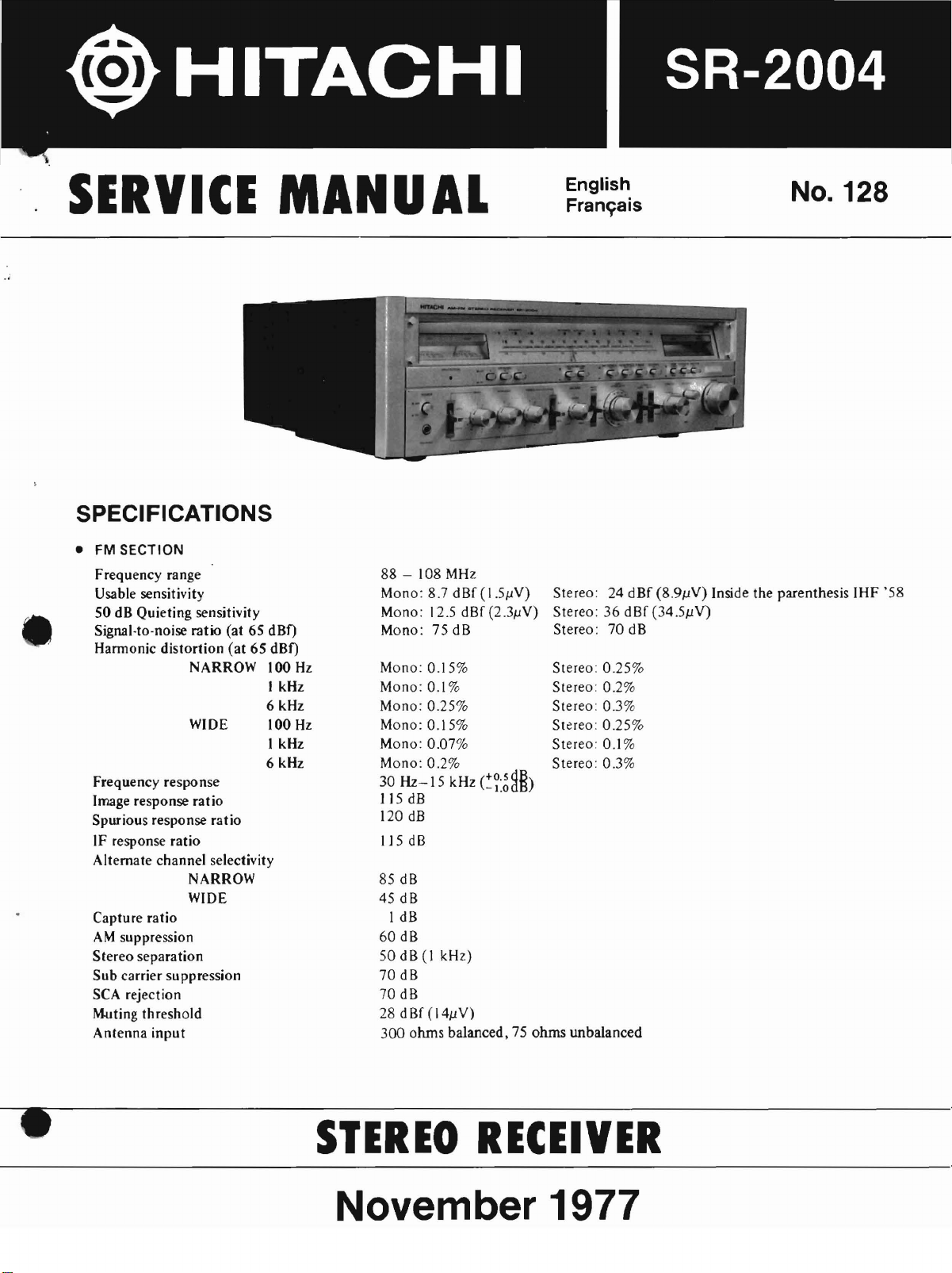
STEREO
RECEIVER
November 1977
Page 2
HITACHI
•
AM
SECTION
Frequency
Sensitivity
Image rejection
IF rejection
Selectivity (IHF)
Signal-to-noise rario
Antenna
•
AUDIO
Output
SR-2004
range
SECTION
RMS
(Both
Music power (IHF)
power
channels driven)
530
- 1,605 kHz
370llY/m(S/N20dB), 20llY (IHF,
70
dB
90
dB
40
dB
50
dB
Ferrite and Separate terminal
200
watts per channel, min. RMS, at 8
from 20 Hz to
0.08
%total harmonic distortion.
230W/ch + 230W/ch (8 ohms, I kHz, T.H.D. 0.08%)
230W/ch
400W/ch +400W/ch (8
+230W/ch
20
kHz, with no more
(4
ohms,
ohms)
ext.
Antenna)
1 kHz, T.H.D. 0.1
%)
e
ohms
than
Power
bandwidth
Frequency
Harmonic distortion
Intermodulation
Input
sensitivity
(at
PHONO
AUX
TAPE-I
TAPE-2
ADAPTOR
DIN
MIC
Max.
input
Output
TAPE OUT
DIN OUT
Signal-to-noise ratio
(IHF,
A-network, rated power)
PHONO
AUX
TAPE
Damping factor
Equalizer
control
Bass
Midrange
Treble
characteristics
(at
rated
(at
'!zrated
(at
rated
(at
'!zrated
200Woutput,
I,
level (PHONO)
level
input
1,2
1,2
control
control
PHONO 2
output)
output)
distortion
output)
output)
shorted,
I kHz)
10 Hz -40kHz
15
PHONO 30 Hz -
10
AUX
Less than 0.08%
Less than 0.03%
0.08%
0.03%
2.5 mY (47 k ohms)
150 mY
150 mY (35 k ohms)
150 mY (35 k ohms)
150 mY (35 k ohms)
450mY(95k
3 mY (50 k ohms)
500
mY
150 mY (PHONO, AUX
200 mY (FM
150 mY (AM
40
mY (PHONOatrated
75 dB
90
dB
90
dB
(l
kHz,8
75
RIAA ±0.2 dB
dB
±10
±10 dB (at 100 Hz turnover frequency
±6 dB (at 1 kHz)
flO
±I0
(at50Hz turnover frequency 150 Hz)
dB (at 10 kHz
dB
(at 20 kHz
Hz -40kHz ±1.5 dB
(50
k ohms)
ohms)
400
400
ohms)
kHz ±0.2 dB
at
rated
Hz, 30% dev.
Hz, 30%
turnover
turnover
mod.
input)
frequency 3 kHz)
frequency 6 kHz)
input)
input:
input:5mY/m)
1 mY)
300
e
Hz)
-2-
•
Page 3

HITACHI
SR-2004
e
Loudness
(Volume
at
High filter
•
Low filter
Audio
Tape
monitor
Speaker switch
Tuning
Power
AC
outlet
Speaker terminal
FM
MUTING/AUTO LOCK
MPX noise filter
IF
BAND filter
MULTIPA
Pre/main amplifiers
Adaptor
Power supply
Power
Dimensions
Weight
control
control
-33
dB position)
muting
meter
consumption
meter
TH
switch
effect
filter
Specifications
set
+9 dB
-10dBat
-10dBat50Hz (12 dB/oct.)
20
-
1,2
A,B,C,A+B,B+C,C+A,OFF
2
2
3
(One
One
Provided
Provided
NARROW
Provided
Separable
Provided
AC
850
580
22-3/4
25.5 kg
and
designs maybechanged
(100
Hz),+4dB
10 kHz (12 dB/oct.)
dB, 0 dB,
touch
120V60
W
(W)
-40
switched50W & 2 unswitched
terminal
and
WIDE
Hz
x
186
(H) x 447 (D)
(W) x 7-1/2 (H) x 17-1/2 (D) in.
(56.2
Ibs.)
without
(10
dB
notice for
kHz)
mm
total
improvement.
150
W)
e
-
CARACTERISTIQUES TECHNIQUES
• SECTION
Bandedefrequence
Sensibilite utilisable
Seuil de sensibilite
Rapport
Distorsion
Reponse
Rapport
Rapportdereception
Rapportdereceptiondemoyenne
frequence
Selectiviteducanal de rechange
Rapport
Suppression
Separation stereo
Filtrage de la sous-porteuse
Rejection SCA
Seuil
Entree de
FM
signal/bruit
harmonique
NARROW
WIDE
de
frequence
de selectivite
NARROW
WIDE
de captage
AM
d'elimination
I'antenne
50
dB
(65
dBf)
(65
dBf)
100
1 kHz
6 kHz
100
1 kHz
6 kHz
non
selective
des parasites
Hz
Hz
88-108MHz
Mono: 8,7
Mono: 12,5
Mono: 75 dB
Mono: 0,15% Stereo: 0,25%
Mono: 0,1%
Mono: 0,25%
Mono:
0,15%
Mono: 0,07%
Mono: 0,2%
30
Hz -15kHz
115 dB .
120
dB
115 dB
85 dB
45 dB
1 dB
60
dB
50dB(1
70
70
28
300
kHz)
dB
dB
dBf(1411V)
ohms
ponderes, 75
V
dBf(1,5I1
dBf
)
(2,3I1V)
e~'~~B)
ohms
Stereo: 24 dBf(8,9I1V)
Stereo:36dBf
Stereo:
Stereo: 0,2%
Stereo: 0,3%
Stereo: 0,25%
Stereo: 0,1%
Stereo: 0,3%
non ponderes
70
(34,5I1V)
dB
Entre
parentheses:
IHF'58
-3-
Page 4
HITACHI
SR-2004
• SECTION
Bande
Sensibilite
Rejet
Rejet MF
Selectivite
Rapport
Antenne
• SECTION
Sortie
Sortie
Bande passante
Distorsion harmonique
Distorsion
Sensibilite d'entree
Niveau
Bornes de sortie
Rapport
Facteur
Compensateur
Commande
Commande
Commande
Sonorite
AM
de frequence
image
(IHF)
signal/bruit
AUDIO
Puissance nominale
Puissance musicale
bande
passante
(a la puissance reelle)
(a la moitie de
d'intermodulation
(a la puissance reelle)
(a la moitie de la puissance
(sous
200W,1 kHz de sortie)
PHONO
AUX
Bande-I
Bande-2
ADAPTOR
DIN
MIC
d'entree
TAPE
OUT
DIN OUT
signal/bruit
(IHF,
reseau A, puissance nominale)
PHONO
AUX
TAPE
1,2
d'attenuation
des graves
des mediums
des aigus
(Ensemble de
volume position
la
puissance reelle)
I,
PHONO 2
maxima (PHONO)
1,2
commande
-33
dB)
rt~elle)
du
530
- 1.605 kHz
370llY/m(S/B 20 dB), 20llY
70
dB
90
dB
40
dB
50
dB
Antenne de ferrite avec borne separee
200
W/ch +
230
W/ch + 230 W/ch(8ohms,
230
W/ch + 230 W/ch(4ohms, 1 kHz, T.H.D. 0,1
400
W/ch +
10 Hz PHONO 30 Hz AUX 10
0,08%
0,03%
0,08%
0,03%
2,5 mY
150
mY
150 mY (35 k ohms)
ISO mY (35 k ohms)
150 mY (35 k ohms)
450
mY (95
3 mY
500
mY
150 mY (PHONO, AUX
200mY(FM
150 mY
40
mY (PHONO a
dB
75
90dB
90
dB
75(IkHz,8
RIAA ±0,2
±IOdB(a
±IO
dB
dB
±6
dB
±IO
dB
±IO
+9dB(100
200
W/ch (8 ohms,20Hz -20kHz, T.H.D. 0,08%)
400
W/ch (8 ohms)
40
kHz
15
Hz-40
(47k
ohms)
(50k
ohms)
kohms)
(50
k ohms)
400
Hz, 30%
(AM
400
Hz, 30%
l'entree
ohms)
dB
50
Hz, frequence de renversement 150 Hz)
(a 100 Hz, frequence
(a I kHz)
(a 10 kHz, frequence de renversement 3 kHz)
(a 20 kHz, frequence de renversement 6 kHz)
Hz), +4dB(10
(Antenne
I kHz, T.H.D. 0,08%)
kHz ±0,2 dB
kHz ±1,5dB
a
l'entree
d'entree
d'entree
nominale)
de
renversement
kHz)
nominale)
dev.: 1 mY)
mod.: 5 mY/m)
ext., IHF)
300
--
%)
•
Hz)
-4-
-
Page 5
HITACHI
SR-2004
e
Filtre haut
Filtre bas
Effet de sourdine audio
ContrOie de bande
•
Interrupteur de haut-parleurs
Indicateur de syntonisation
Indicateur de puissance
Sortie C.A.
Borne de haut-parleur
FM
MUTING/AUTO LOCK
Filtre de bruit parasite
Filtre de bande FI
Filtre de trajets multiples
Preampli/Ampli principal
Commutateur d'adaptateur
Alimentation
Consommation
Dimensions
Poids
Les
caracteristiques techniques et la presentation peuvent etre modifiees sans preavis par suite d'ameIiorations.
MPX
-10
dB
a10 kHz (12 dB/oct.)
-10
dB
a50 Hz (12 dB/oct.)
-20
dB, 0 dB, - 40
1,2
A,B,C,A+B,B+C,C+A,OFF
2
2
3 (Unede50 W raccordee, et deuxde150 W non raccordee)
Borne
aune touche
Incorpore
Incorpore
Position WIDE
Incorpore
Separes
Incorpore
Secteur 120 V 60
850W
580 (L) x 186 (H) x 447 (P) mm
25,5 kg
dB
et
NARROW
Hz
e
-
IMPORTANT NOTICE "
(1) When measuring the output power or listening
program sources with the 4-0HMS load impedance,
do not drive the Model SR-2004 at full power for a
long period
(2) When using the model with a continuous
over 200 watts, the protection indicator will light
up and the sound will sometimes be interrupted.
This does not indicate a breakdown. In such cases,
tum
then wait 30 seconds before switching the power
back on again.
(3) The Model SR-2004 has two types
of
time.
off
the power, turn down the volume level and
of
electronic pro-
output
to
of
tection circuits; a shut-down circuit and current
If
limiter circuit.
outputofthe amplifieriscut off.
the
When only the current limiter circuit
the operation
down.
(4) Before taking
and MAIN IN terminals on the rear panel, make sure
that POWER switch
attenuator volume
(5) Set the
you are not using the microphone.
MIC
the shut-down circuitisactuated,
is
of
the power amplifierisnot
off
the couplers from the PRE OUT
is
settoOFF and
is
settothe lower position
MIXING volume controltoOFF when
actuated,
that
(00).
AVERTISSEMENT IMPORTANT
(1) Quand on mesurelapuissance en sortie ou que I'on
ecoute des sources de programmes avec I'impedance
de
charge de 4-ohms,nepas faire fonctionner
Ie
modele SR-2004 apleine puissance pendant une
longue periode de temps.
on
(2) Quand
de puissance depassant 200 watts,
tection peut s'allumer et
s'interrompre. Ceci ne veut pas dire qu'il y ait une
panne. Dans de tels cas, couper l'alimentation, baisser
secondes avant de reaIimenter I'appareil.
Le
(3)
cuits de protection electronique; un circuit d'arret
utilise cet appareil avec un debit continuel
Ie
Ie
niveau du son, et puis attendre environ 30
modele SR-2004 est equipededeux types de cir-
Ie
voyant de pro-
son peut quelquefois
total et un circuit de limitation
cas oilIecircuit de coupure totale est active, la sor-
de
I'amplificateur est coupee.
tie
Ie
Quand seul
active, l'amplificateur continue
(4) Avant
(5) Mettrelacommandedevolumedemelange micro
,pasIemicrophone.
de
nes PRE OUT et
prendre bien soin
d'alimentation est bien
et
(arret)
position la plus basse
(MIC
MIXING) surlaposition OFFsivous n'utilisez
circuitdelimitation de courant est
retirer les barres d'accouplement des bor-
MAIN
de
verifier queIecommutateur
queIevolumedeI'attenuateur est sur la
(00).
de
courant. Dans
afonctionner.
IN
du panneau arriere,
mis
sur1aposition OFF
shut
the
"-
Ie
-5-
Page 6
HITACHI
SR-2004
FEATURES
Tuner
Section
1.
Dual Gate MOS FET for High QualityFMTuner
Three Dual Gate MOS
variable capacitors offer excellent
(I.5j1V), intermodulation characteristics, high S!N ratio
and
spurious rejection.
2.
Auto-Lock
To
stabilize tuning, an
This circuit engages immediately when
tuning
tuning
for
(the
Releasing
circuit which automatically stabilizes the tuning circuit
and
and
3.IFBAN
SAW
IF
BAND selector switchisprovided in the
to
provide a selectivity
conditions.
In the WIDE position,
superior group delay characteristics in the wide frequency range, and
FILTER
In the NARROW position,
CERAMIC
interference sharply by high selectivity.
4.
High-Selectivity and Low-Distortion IF Amplifier using
IC's
and
A 6-stage differential amplifier
sive use
IF stage,
IF amplifier greatly improves
characteristics.
5.
Quadrature
Quadrature detection
a wide
6.
Phase-Locked LoopICfor
A PLL-IC, which was developed
the
FM!MPX circuit for a high separation
tortion.
temperature
7.
Reed Relays for Cutting
In the
vided in
noise.
8.
MPX NOISE FILTER
Sometimes
obtaining
receivers,
reduce this noise.
The
noise
9.
FM
MULTIPATH Switch with Meter
Reception
Direct signals and signals reflected by mountains and
buildings cause a multipath effect. This increases distortion
To
eliminate this trouble, thereisa
circuit which operates together with
10.
3-gang Variable Capacitor for High Selectivity
Reception
A 3-gang variable capacitor
sensitivity and selectivity during
-------------------
FET'sinthe
Circuit
knob
after precise tuning.
knob,
you can disengage
Auto-Lock indicator goes
the
tuning knob re-engages
locks
onto
the station selected for a high S!N ratio
low distortion.
D Selector Switch for Flexible Selectivity and
FI
LTER for Low Distortion
offer sound with
FILTER
3 Ceramic Filters
of3Ie's,
that
have good phase characteristics, in the
Detection
band
coverage and low
Also, high reliabilityisachieved with respect to
and aging.
FM
MUTE position,
FM
audio
high frequency noise prevents
hi-fidelity
you
havetolistentobroadcastsinmono
MPX NOISE
without
imparing
and downgrades separation.
Auto-Lock
that
the
the
4-pole
extra
will also
and
two
ceramic filter elements in the
with
the
FM/MPX Circuit
out
output
FM
stereo reception. With some
FILTER
can be usedtoreduce this
theFMstereo effect.
is
front-end
circuitisprovided.
Justbytouching the
the
Auto-Lock circuit
off)
fine tuning.
meets different receiving
SAW
FILTER,
LC
LINEAR PHASE
low distortion.
the
2 LINEAR PHASE
operatetocut
is
employed.
the
limiter and selectivity
extensive useofIe's
distortion.
by
Hitachi,isused for
Detuning Noise
two
Reed Relays are pro-
stage
to
cut
for
multipath
the
provided for achieving high
AM
reception.
and
5-gang
FM
sensitivity
you
release the
the
Auto
FM
IF stage
which has
out
The exten-
and
low dis-
out
detuning
you
Best
FM
detection
signal meter.
AM
Lock
the
FM-
has
from
to
11. Ceramic Filter,
A ceramic filterisemployed in
enhanced
sive use
12.
Two
wheel Tuning Knob
Two
and
The dial mechanism employs a large-sized fly-wheel with
a high
Audio
1. Newly Developed High-Efficiency High-Power
Amplifier (Series E ..... Class GorDynaharmony
Amplifier)
This amplifier delivers a higher
(400
conventional class-B amplifiers.
The
tion minimizes the
the weight
This amplifier has twin
Under this
namic power which
maximum
2. Twin Power Meters
To
combined
3.
Midrange
This amplifier has
controls
By
ferred frequency characteristics
The
This feature offers good feel which makes for easier setting
Turnover
4.
This model has
low
Each switch has two turnover frequency settings.
In
touching
provided. You can adjust the frequency characteristics
to
andtosuit
5.
Calibrated
A precisely calibrated 32- click-stop
uatorisused for the volume
easier setting and resetting
level.
Audio
6.
This switch
without
between
Further,
of
attenuator
7. Mic Mixing
A mic mixing circuit
Just
sounds from the microphone
sources.
of
Large Easy-to-Read Meters
easy-to-read meters are usedtoindicate the signal
tuning
momentofinertia for easy operation.
Section
W per channel, 8 ohms)
relative low power
see
the
setting these three controls,
controls all have11click-stop
and
and
ordertomake flat frequency characteristics
meet
Muting Switch
output
connect
ICsinAM
selectivity and AGC characteristics. The exten-
Ie's
improves stable reception.
levels.
------------------
and
sizeofthe whole amplifier.
method,
rated
output
actual power
two new attractive
Tone
Control
but
also a MIDRANGE
resetting.
and Tone Defeat Switches
high frequency characteristics independently.
touching the level
two
a more precise and flexible setting
two
tone
controls
the acoustic conditionsofyou
your
taste.
Attenuator
is
very useful when lowering
attenuation values
level can be achievedbycombining the level
and the muting switch.
a microphone and
Tuner
the
AM
tunertoobtain
and
a Large-sized Fly-
Audio
dynamic
without
consumptionofclass G opera-
heal
sinkofthe
DC
power supplies.
c1ass-G
is
more
powerormore.
(L
and R channels)
output
not
only BASS
turnover switches for adjusting the
tone
(Volume Control)
is
incorporated
power transistors and
operation
than
twice the valueofthe
while
power
tone
you
of
the
contact
defeat functions are also
control.
of
the
desired power
attenuator.
(-20dB,
you
with
oUlpuCpower
distortion than
can deliver dy-
you
meters are provided.
in this model.
are listening,
and
TREBLE tone
control.
can choose
amplifier.
points.
listening room
contact
will be abletomix
point
This makes for
the
sound level
You can choose
-40dB).
and
other
the
pre-
without
atten-
output
resetting
program
e
e
•
-6-
Page 7
HITACHI
SR-2004
-
•
-
8. Tape Dubbing
Tape dubbing can be done either from TAPE-I
2 or vice versa. There
with which tape dubbing
FM
•
broadcast or a record.
9. Low Filter and High Filter
The low filter cuts
rumble from a turntable and the high filter cuts out the
high frequency noise such
records and high frequency noise while listeningtoFM
broadcasts.
out
CARACTERISTIQUES
Section Tuner
1.
MOSFET
qualite
Les trois
d'attaque
permettentd'obtenir
IlV), des caracteristiques d'intermodulation,unrapport
signal/bruit tres eleve et une suppression des parasites.
2. Circuit auto-verrouillable
Pour stabiliser la syntonisation,uncircuit auto-verroui!lable est installe. Ce circuit s'enc1enche immediatement
des que vous reliichezIebouton
avoir
bouton
auto-verrouillable (Ie voyant du circuit s'eteint), pouvant
proceder ainsi
lachez
auto-verrouillable
stabilisant ainsiIecircuit de syntonisationetIe
sur la station emettrice
nir un rapport signal/bruit
sion.
3. Selecteur de bande
flexibilite de choix
distorsion
commutateur
Un
installe dans l'etage
une
de reception. Sur la position WIDE (large),
qui possede des caracteristiques elevees de retard de
groupe dans
de phase lineaire
sons pratiquement
NARROW
lineaire seront actives aussi pour supprimer
toutes les interferences du fait de leur haute selectivite.
4. Amplificateur de
utilisant des 3 circuits
On utilise un amplificateur differentiel
sation continuelle de 3 circuits
de filtre ceramique dans l'etage FI, qui possectent d'excellentes caracteristiques de phase, de l'amplificateur
FM, ameliore grandement les caracteristiques de selecti·
viteetde limitation.
5.
Detection quadriphonique
La detection quadriphonique,
cuits
largeetune distorsion faible.
-------------------
adouble porte pour un Tuner
MaS
FET
a double porte montes dans l'etage
et les 5 groupes de condensateurs variables
une sensibilite
obtenu
selectivite
integres, permet d'obtenir une bande passante tres
un accord parfait. C'est justeentouchant
de syntonisation que vous desactivezIecircuit
a nouveauIebouton
a une syntonisation precise. Quand vous
se
FI
(IF BAND) pour une grande
et
un filtre
selecteur de bandeFI(IF
FI
qui
s'adapte a n'importe quelle condition
Ie
domaine des frequenceslongues,etIe
LC
a 4 poles permettent
denues de distorsion. Sur la position
(etroite),
les deux filtres ceramiques de phase
haute
integres
to
is
also a source
is
possible whi!e listeningtoan
the low frequency noise such
as
noise from scratches
de syntonisation,Iecircuit
reenc1enchera
desiree, ce qui
tres eleve et une faible distor-
SAW
FM
pour vous permettre d'avoir
selectivite
et
integresetde 2 elements
a l'aide de
monitor
FM
FM
excellente (1,5
de syntonisation apres
automatiquement
permettra
pour une faible
et
abasse distorsion
2 filtres aceramique
a 6 etages. L'utili-
TAPE-
circuit,
de haute
bloquant
d'obte-
BAND) est
Ie
filtre
d'obtenir
pratiquement
nombreux
on
SAW
filtre
des
cir-
as
Ie
FI
10. Three Speaker Systems Connection
Three speaker systems can be connected
selected with switches.
11. Electronic Protection Circuit
Hitachi's original, highly reliable electronic
circuitisbuilt-in
transistors. When a fault occurs, the circuit
off
and thisisthen
light emitting diode.
12. Adaptor Switch
This function
deck or for a Dolby
6.
Circuit FM!MPX aboucle de blocage de phase equipee
de circuits integres
Un circuit integre PLL, developpe par Hitachi, est utilise
pourIecircuit FM/MPX, permettant ainsi
haut degre de separation et une faible distorsion. On a
egalement une
consideration la temperatureetla duree de service.
7.
Relais alame
Dans la position
lame dans I'etage de sortie
desaccordants.
8. Filtre de bruit
Quelquefois, des parasites de haute frequence vous emptkhent
stereophonique. Avec quelques recepteurs,ilvous faut
ecouter ces emissions au mode Mono afin
niveau des parasites. Le mtre de bruit MPX (MPX
NOISE
parasites sans nuire
9.
Commutateur
PATH) avec indicateur pour obtenir une reception
encore meilleure
L'addition des signaux directs et de ceux qui viennent,
refletes par des montagnes ou des batiments par exempie, jusqu'a votre appareil produit
l'effet
et augmente
probleme,
trajets multiples
cateur de signaux.
10. Condensateur variable
elevee
Un condensateur variable a 3 groupes est installe, ce qui
permet d'avoir un niveau de sensibilite et de
tres eleve
11. Filtre ceramiqueetcircuits integres dansIetuner
On utilise un nItre ceramique dansIetuner
obtenir une selectivite plus eleveeetdes caracteristiques
AGC. L'utilisation
la
12. Deux indicateurs grands
syntonisation de grande taille
Deux indicateurs grands
pour indiquer les niveaux
Le mecanisme d'accord est
grande taille
noeuvres.
d'obtenir
FILTER)
a trajets multiples. Cet effet diminue la separation
il
en reception
pendant
stabilite de la reception.
to
protect the speakers and power
displayed on the front panel by the
is
very convenient for using a third tape
NR
adaptor.
tres haute fiabilite quand
pour
supprimer les bruits desaccordants
FM
MUTE,ona installe deux relais a
FM
qui suppriment les bruits
MPX
(MPX NOISE FILTER)
une reception
peut
etre utilise pour reduirecegenre
a l'effetFMstereo.
FM
de trajets multiples (FM MULTI-
Ie
niveau de distorsion. Pour supprimer ce
y a
un
circuit de detection de l'effet de
qui
est active en meme temps que l'indi-
FM
a3 groupes pour une selectivite
AM
la reception
tres large de circuits integres ameliore
et
a inertie elevee,cequi facilite les ma-
AM.
et
faciles alire
et
faciles a lire ont ete installes
du
signaletde syntonisation.
eqtiipe
to
the unit and
is
d'obtenir
on
de haute-fidelite
de
ce
qu'on
selectivite
etunbouton
d'un
bouton
protection
switched
un
prend
en
et
reduire
AM
Ie
FM
appelle
AM
pour
de
de
-7-
Page 8
HITACHI
SR-2004
Section
Audio-----------------
1. Amplificateur audio nouvellement developpe agrande
puissance
et
ahaute efficacite (serie E
...
c1asse
G. ou
Amplificateur Dynaharmonique)
Ce
nouvel amplificateur
dynamique
8
ohms)
ventionnelsdec1asseB.La
relativement
nue
sance
Cet
continuo Avec
amplificateurs
puissance
du
debit
encore plus elevee
sans distorsion
basse des
les
effets
de la chaleur
et
abaisseIepoidsetla tailledel'amplificateur.
amplificateur
cette
de classe G
dynamique
maximum
fournit
comme
amplificateursdec1asse
possede 2
methode,Iefonctionnement
de plus de
de puissance.
une
sortie de puissance
(400
watts
les amplificateurs
consommation
sur
les transistors de puis-
alimentations
peut
permettre
deux
fois la valeur fixee
par canal, sous
de puissance
G dimi-
en
courant
d'obtenir
2. Indicateurs doubles de puissance (Canaux L (gauche)
R (droit))
Pour
voir la puissance en sortie
musique,
elegants.
3.
Commande de tonalite du haut-parleur medium
Cet
man
(TREBLE),
parleur
En
choisir
rez
\Ces
,par
Ivres
4.
t:ommutateurs
on
a installe
amplificateur
des de tonalite
medium
reglant ces trois
Ie,s
caracteristiques de
pour
votre
commandes
c1iquets. Ce systeme
suresetainsi des reglages
est equipe
pour
mais aussi
(MIDRANGE).
commandes,
amplificateuf.
ont
tous
d'une
de renversementetd'amortissement de
deux
les graves (BASS)etles aigus
leurs
permet
tout
indicateurs
non
seulement
commande
vous
frequences
points
d'effectuer
nombreux
en
ecoutant
nouveaux
de com-
pourIehaut·
etes
capable de
que
vous prefe-
de reglage aarrets
des manoeu·
plus facilement.
tonalite
Cet
appareil est equipe de
sement
tiquesdehautesetbasses frequences. De plus,
commutateur
frequence.Setrouvent
d
teristiques
aux
gouts
5.
Attenuateur
Un
points
mande
reglages
desire de sortieenpuissance.
6.
Commutateur
Ce
niveau du son sans
Vous
ment(-20dBet-40
En
du
commutateur
niveau.
7.
Melange micro
Cet
suffitderaccorderunmicrophoneetil
d'effectuer
microphoneetdes sons
8.
Copiage de bande
On
TAPE-l
cuit
un copiage de
radio
permettant
possede
'amortissement
conditions
personnels.
pour
de frequences de
acoustiques de la piece
calibre (commandedevolume)
attenuateur
de
du niveau sonore. Ceci
nombreux
calibre de far;on
contacts
de sourdine audio
commutateur
pouvez choisir entre
outre,onpeut
niveau de sortiesion
appareil est equipe
peut
effectuer
sur
de contr61e de source avec lequelonpeut
FM
ouaun
est tres utile
de niveau avec celui de
des melanges
TAPE-2ouinversement.IIy a aussiuncir·
bande
disque.
deux
de regler
deux
vous
a c1iquets est utilise
et plus faciles
toucheral'attenuateur
dB).
obtenir
d'un
d'autres
des copiage de
toutenecoutantaune
commutateurs
separement
positions
aussi
permettrederegler les carac-
fa<;on
deux
des
combine
circuit de melange micro.
entre
de renversement de
incorporees,
aconvenir
tres
permet
pour
quandonveut abaisser
valeurs d'assourdisse-
n~glages
les manoeuvres du
des sons provenant du
sources de programme.
bande
de renver-
les caracteris·
chaque
des fonctions
Ie
pour
de niveau.
plus varies
proceder a
emission
mieux
la com·
d'ecoute,etavos
precise et a
de proceder a des
obtenirIeniveau
encore
l'attenuateur
vous sera possible
soit a partir de
con·
des
une
et
32
et
de
9.
Filtres
hautetbas
Le filtre bas supprime les parasites de basses frequences
commeIeronflement
Ie
filtre
haut
comme
supprime
pendant
supprime les parasitesdehautes
les
bruits
egalement les parasites de
l'ecoute
provenant
provenant des rayures
d'emissions radio FM.
d'un
tourne-disque, et
frequences
d'un
disque
hautes
frequences
e
et
10. Possibilite de branchement pour trois enceintes
acoustiques
On
peut raccorder 3 enceintes
et
les selectionner a l'aide de
acoustiquesacet
commutateurs.
appareil
11. Circuit de protection electronique
Hitachi
tection
proteger
Quand
la
Ie
diode
12.
Commutateur
Cette
troisieme piatine de
teur
a incorpore dans
electronique
les hauts-parleurs et les
une
fonctionnement
fausse manoeuvreseproduit,Iecircuit arrete
a emission lumineuse situee
originaletde
et
ce fait est alors indique par
d'adaptation
fonction
Dolby
NR.
est tres
commode
magnetophoneoupour
cet
appareil
haute
transistors
surIepanneau
quand
son
circuit de pro-
fiabilite afin de
de puissance.
on
utilise une
un adapta-
la
avant.
e
Ie
11
•
Page 9
~
•
e
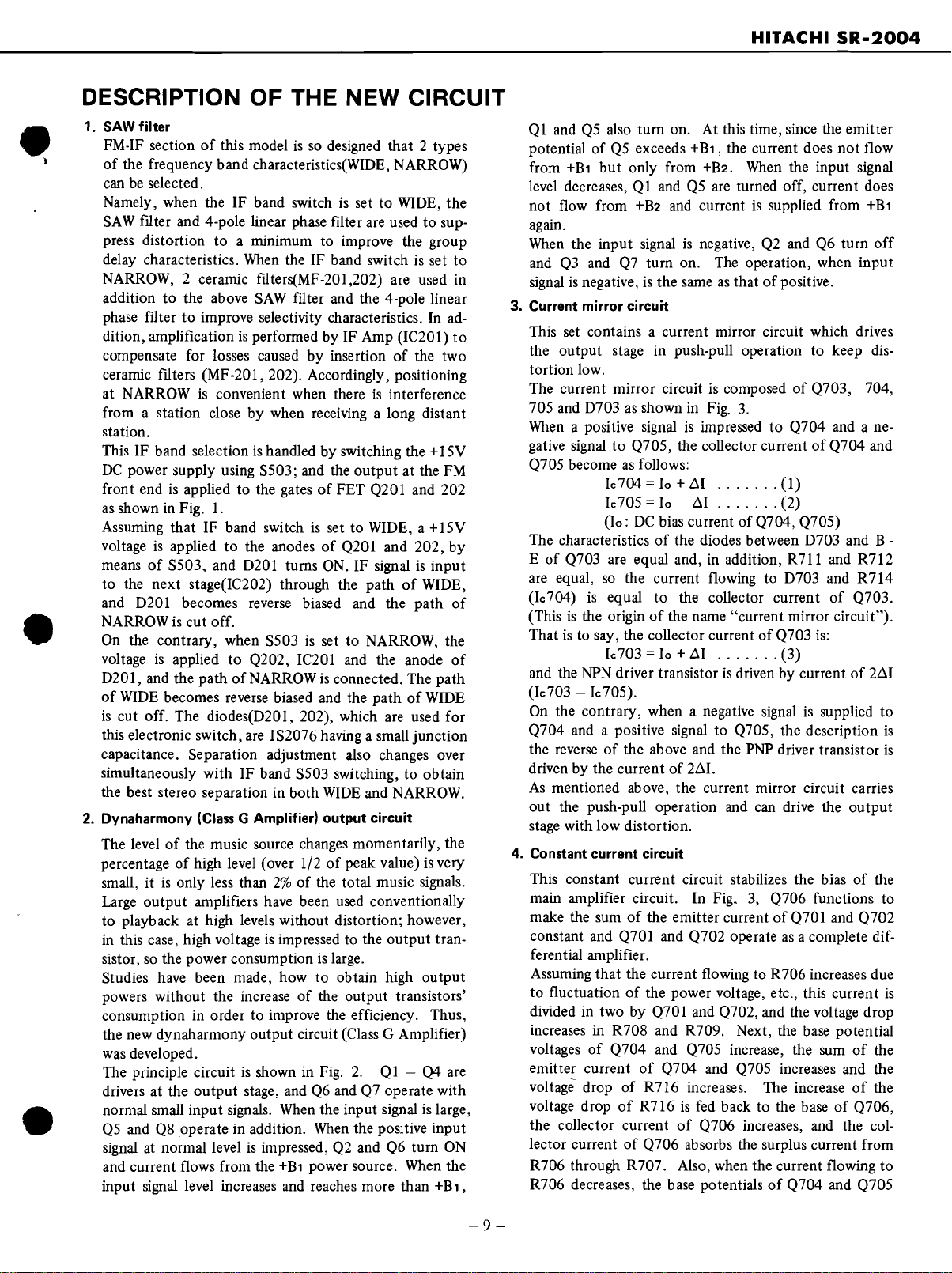
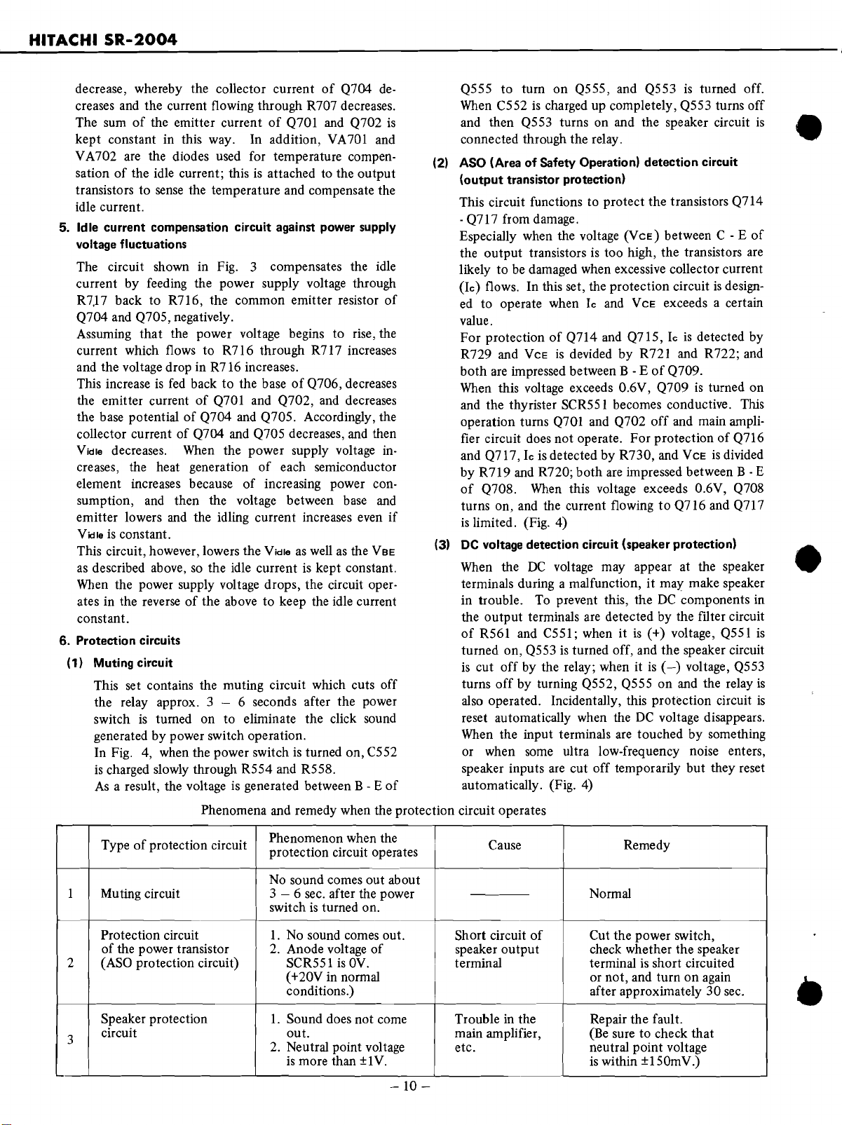
DESCRIPTION OF THE NEW CIRCUIT
1.
SAW filter
FM-IF sectionofthis modelisso
of
the frequency band characteristics(WIDE, NARROW)
can be selected.
Namely, when the IF band switch
SAW
fIlter and 4-pole linear phase filter are usedtosuppress distortion
delay characteristics.
NARROW, 2 ceramic ftlters(MF-201,202) are used in
addition
phase filter
dition, amplification
compensate for losses causedbyinsertionofthe two
ceramic
at NARROW
from a station close by when receiving a long distant
station.
This IF band selection
OC
front endisappliedtothe gatesofFET Q201 and 202
as
Assuming
voltage
meansofSS03, and
to
and
NARROWiscut
On the contrary, when SS03
voltage
0201,
of
is
this electronic switch, are IS2076 having a small junction
capacitance. Separation adjustment also changes over
simultaneously with IF band SS03 switching,
the best stereo separation in both
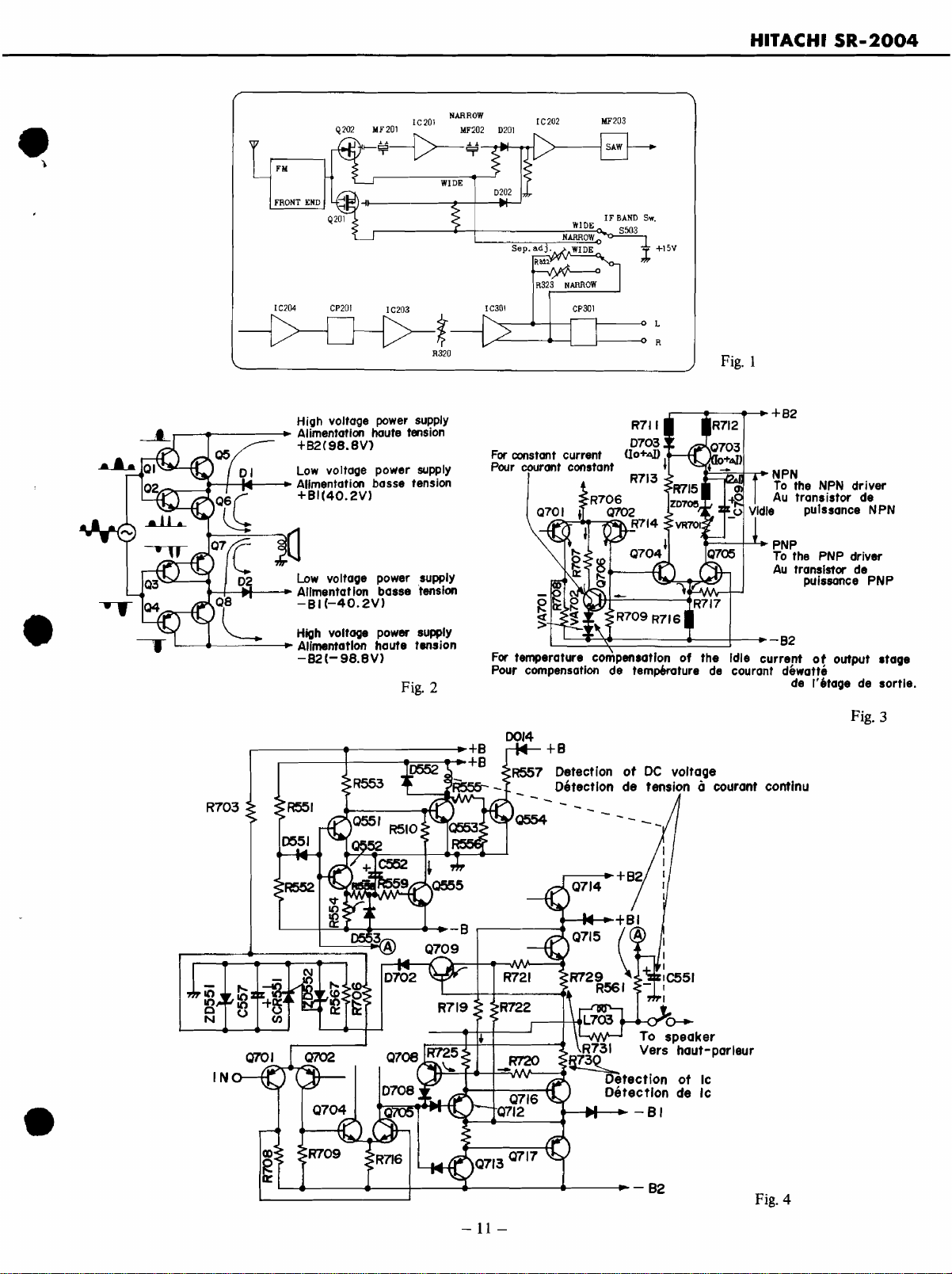
Dynaharmony
2.
The levelofthe music source changes momentarily, the
percentage
small, it
Large
to
in this case, high voltage
sistor,
Studies have been made, how to obtain high
powers without the increaseofthe output transistors'
consumption in order
the new dynaharmony output circuit (Class G Amplifier)
was developed.
The principle circuit
drivers at the
normal small input signals. When the input signal
QS
signal at normal level
and current flows from the
input signal level increases and reaches more than
to
fIlters (MF-201, 202). Accordingly, positioning
power supply using SS03; and the
shown in Fig.
is
the next stage(lC202) through the pathofWIDE,
0201
is
and the
WIDE
becomes reverse biased and the pathofWIDE
cut off. The diodes(0201,202), which are used for
is
output
playback at high levels without distortion; however,
so
the power consumptionislarge.
and Q8 operate in addition.
to
a minimum to improve the group
When
the above
to
improve selectivity characteristics. In ad-
is
that
IF band switchissettoWIDE, a +ISV
appliedtothe anodesofQ201 and 202,
becomes reverse biased and the
applied
pathofNARROWisconnected. The
(Class
of
high level (over 1/2ofpeak value)isvery
only less than2%of
amplifiers have been used conventionally
output
SAW
is
performed by IF Amp (lC201)
convenient when thereisinterference
is
handled by switching the +ISV
1.
0201
off.
to
Q202, IC201 and the anode
G Amplifier) output circuit
is
impressed to the
to
improve the efficiency. Thus,
is
shown in
stage, andQ6and Q7 operate with
is
impressed, Q2 and Q6 turn
+B1
designed that 2 types
is
settoWIOE, the
the IF band switchisset
filter and the 4-pole linear
to
output
turns ON. IF signalisinput
is
settoNARROW, the
WIDE
the total music signals.
Fig.
2.
When
the positive input
power source. When the
at the
FM
by
path
path
to
obtain
and NARROW.
output
QI - Q4 are
tran-
output
is
large,
ON
+B1,
of
of
to
HITACHI
QI andQSalso turn on. At this time, since the emitter
potential
from
level decreases,
not flow from
again.
When
and
signalisnegative,isthe sameasthatofpositive.
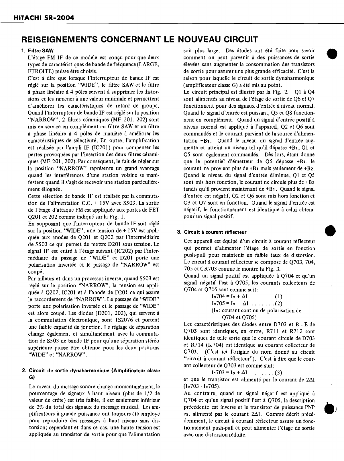
3. Current mirror circuit
This set contains a current mirror circuit which drives
the output stage in push-pull operation
tortion low.
The current mirror circuit
705 and
When
gative signal
Q70S become
The characteristics
E
are equal,
(le704)
(This
That
and the
(Ie703 -Ie705).
On
Q704 and a positive signaltoQ70S, the description
the reverseofthe above and the PNP driver transistor
driven by the currentof261.
As
out the push-pull operation and can drive the
stage with low distortion.
4. Constant current circuit
This constant current circuit stabilizes the biasofthe
main amplifier circuit. In Fig.
make the sum
constant and Q701 and Q702 operate
ferential amplifier.
Assuming
to
divided in two by Q701 and Q702, and the voltage drop
increases in R708 and R709. Next, the base potential
voltages
emitter current
voltage drop
voltage drop
the collector current
lector current
R706 through R707. Also, when the current flowing
R706 decreases, the base potentialsofQ704 and Q70S
ofQSexceeds
+B1
but
only from +B2. When the input signal
Ql
+B2
the input signalisnegative,
Q3
and
Q7
0703asshown in Fig.
a positive signalisimpressedtoQ704 and a ne-
to
Q70S, the collector currentofQ704 and
as
follows:
le704
Ie
705 =
(10:
OC
of
Q703 are equal and, in addition, R711 and R712
so
the current flowing to
is
equal
is
the originofthe name "current mirror circuit").
is
to say, the collector currentofQ703 is:
le703
NPN
driver transistorisdriven by currentof261
the contrary, when a negative signalissupplied
mentioned above, the current mirror circuit carries
of
that
the current flowing to R706 increases due
fluctuationofthe power voltage, etc., this current
of
Q704 and Q70S increase, the sumofthe
of
of
of
R716isfed backtothe baseofQ706,
of
+B1
, the current does
and
QS
are turned off, current does
and currentissupplied from
Q2
and Q6 turn
turn on. The operation, when
is
composedofQ703, 704,
3.
=
10
+61
10
- 61 (2)
bias currentofQ704, Q70S)
of
the diodes between
to
the collector current
=
10
+61
the emitter currentofQ701 and Q702
Q704 and Q70S increases and the
R716 increases. The increaseofthe
of
Q706 increases, and the col-
Q706 absorbs the surplus current from
(1)
0703
(3)
3,
Q706 functions to
as
SR-2004
not
to
keep
0703
and R714
of
a complete dif-
flow
+B1
off
input
dis-
and B -
Q703.
to
is
is
output
is
to
-9-
Page 10
HITACHI
SR-2004
decrease, whereby the collector currentofQ704
creases and the current flowing through R707 decreases.
The sum
kept constant in this way. In addition,VA701
VA702 are the diodes used for temperature compen-
sation
transistors to
idle current.
5. Idle current compensation circuit against power supply
voltage fluctuations
The circuit shown in Fig. 3 compensates the idle
current by feeding the power supply voltage through
R7,17
Q704 and Q705, negatively.
Assuming that the power voltage begins to rise, the
current which flows to R716 through R717 increases
and the voltage drop in R716 increases.
This increase
the emitter current
the base potential
collector current
Vidle
creases, the heat generation
element increases because
sumption, and then the voltage between base and
emitter lowers
Vidleisconstant.
This circuit, however, lowers the
as
When
ates in the reverse
constant.
6.
Protection circuits
(1)
of
the emitter currentofQ701
of
the idle current; thisisattached to the output
sense
the temperature and compensate the
back to R716, the common emitter resistor
is
fed
back to the baseofQ706, decreases
of
Q701 and Q702, and decreases
of
Q704 and Q705. Accordingly, the
of
Q704 and Q705 decreases, and then
decreases.
described above,sothe idle currentiskept constant.
the power supply voltage drops, the circuit oper-
Muting circuit
This set contains the muting circuit which cuts off
the relay approx. 3 - 6 seconds after the power
switch
generated by power switch operation.
In Fig.
is
As
is
charged slowly through R554 and R558.
a result, the voltageisgenerated between B - E
When
the power supply voltage
of
each semiconductor
of
increasing power con-
and
the idling current increases even
Vidleaswellasthe
of
the above to keep the idle current
turned on to eliminate the click sound
4,
when the power switchisturned on, C552
and
de-
Q702
and
in-
VeE
is
of
of
Q555 to turn on Q555, and Q553isturned off.
When
C552ischarged up completely, Q553 turns off
and then Q553 turns on and the speaker circuit
connected through the relay.
(2) ASO (AreaofSafety Operation) detection circuit
(output transistor protection)
This circuit functions to protect the transistors Q714
-Q717 from damage.
CE)
Especially when the voltage (V
the output transistorsistoo high, the transistors are
be
likely to
(Ie) flows. In this set, the protection circuit
ed
to operate whenIeand VCEexceeds a certain
value.
For protection
R729 and
both
When
and the thyrister SCR551 becomes conductive. This
operation turns
fier circuit does not operate. For protection
and Q717,
by R719 and R720;
of
Q708.
if
turns on, and the current flowing
is
limited. (Fig. 4)
(3)
DC
voltage detection circuit (speaker protection)
When the
terminals during a malfunction,
in trouble. To prevent this, the
the output terminals are detected by the filter circuit
of
R561 and C551; when itis(+) voltage, Q551
turned on, Q553isturned off, and the speaker circuit
is
cut off by the relay; when itis(-)
turns
also operated. Incidentally, this protection circuit
reset automatically when the
When the input terminals are touched by something
or when some ultra low-frequency noise enters,
speaker inputs
automatically. (Fig. 4)
damaged when excessive collector current
of
Q714 and Q715,Ieis
VCEisdevided by R721 and R722; and
are
impressed between B - EofQ709.
this voltage exceeds 0.6V, Q709isturned on
Q701
and Q702 off and main ampli-
Ieisdetected by R730, and VCEis
both
are impressed between B - E
When
this voltage exceeds 0.6V, Q708
DC
voltage may appear at the speaker
off
by turning Q552, Q555 on and the relay
are
cut off temporarily but they reset
between C - E
detected by
to
Q716 and Q717
it
may make speaker
DC
components in
voltage, Q553
DC
voltage disappears.
is
design-
of
Q716
divided
is
e
of
•
is
is
is
Phenomena and remedy when the protection circuit operates
of
Type
1 Muting circuit 3 - 6 sec. after the power Normal
Protection circuit
of
2 (ASO protection circuit) SCR551
Speaker protection
circuit
3
protection circuit
the power transistor
Phenomenon when the
protection circuit operates
No sound comes out about
switch
is
turned on.
1.
No sound comes out. Short circuit
2. Anode voltage
(+20V in normal
conditions.) after approximately
1.
Sound does not come Troubleinthe Repair the fault.
out.
2. Neutral point voltage
is
more than
of
is
OV.
±lV.
Cause
of
speaker output check whether the speaker
terminal terminalisshort circuited
main amplifier,
etc. neutral point voltage
Cut the power switch,
or not, and turn on again
(Be
sure to check that
is
within ±150mV.)
-10-
Remedy
30
sec.
•
Page 11
HITACHI
SR-2004
.~
•
I
~
."
I.
'i
CP301
I 0 L
MF203
IF
BAND
S503
Sw.
,1
+15V
R
Fig. 1
I •
t· -:.. J
+~
:"'01
• I
••
1"
I
Vldle
I.
+82
NPN
To
the
NPN
Au
transistor de
puissance NPN
PNP
To
the
PNP
Au
transistor
puissance PNP
driver
driver
de
Sep.
IC202
adJ.
~
MF201
IC201
supply
tension
supply
'tension
*
NARROW
..L~
'=F
IC30\
Q202
1-E!i-{>-MF202
T
lC204
14
•
1M'"
"'201
Hioh voltage
..
Alimentation
+B2C98.8V)
Low
voltaoe power
• Alimentation basse tension
+BI(40.2V)
Low
voltaoe power supply
Allmentat
-BIC-40.2V)
Ion
le203
power
haute
basse
•
High
volt*
"
R703
It)
II')
C
N
IN
• Alimentation haute tension
-82{-98.8V)
power
supply
Fig. 2
I'
T
\~
For
temperature compensation
Pour compensation
00'4
de
of
temperoture
ot
de
• I
the Idle currentotoutput
de
Ie
Ie
..
82
courant dewatte
deI''tagedesortie.
eontlnu
.tage
Fig. 3
•
I It It I ,
-11-
•
...-82
Fig. 4
Page 12
HITACHI
SR-2004
REISEIGNEMENTS CONCERNANT
1. Filtre
2. Circuitdesortie dynaharmonique (Amplificateur classe
SAW
L'tHage
types de caracteristiques de bande
ETROITE) puisse
C'est
regle sur la position "WIDE",IefIltre
aphase lineaire a4 poles servent asupprimer
sions et les ramener
d'ameliorer les caracteristiques
Quand l'interrupteur
"NARROW", 2
mis,en service en
a phase lineaire a 4 poles
caracteristiquesdeselectivite.Enoutre, l'amplification
est
pertes provoquees par l'insertion des deux fIltres ceramiques (MF 201, 202). Par consequent,
la position "NARROW"
quand les interferences d'une station voisine
festent quand
ment
Cette selectiondebande IF est realisee par la commutation de l'alimentation C.C.
de l'etage d'attaque
Q20l
En supposant que l'interrupteur de bande IF soit
sur la position "WIDE", une tension de +
quee aux anodesdeQ201 et Q202 par l'intermediaire
de S503 ce qui permetdemettre D201 sous tension.
signal IF est entre al'etage suivant (IC202) par l'inter-
mediaire du
polarisation inversee etIepassage de "NARROW" est
coupe.
Par ailleurs et dans un processus inverse, quand S503 est
regIe sur la position "NARROW", la tension est appli-
quee aQ202, IC201 et al'anode
Ie
porte une polarisation inversee et
est alors coupe.
la commutation electronique, sont IS2076 et portent
une faible capacite
change egalement et simultanement avec
tion de S503
superieure puisse etre obtenue pour les deux positions
"WIDE"
FMIFdecemodele est con9u pour que deux
de
fnlquence (LARGE,
etre choisis.
adire que lorsque l'interrupteur de bande IF est
SAWetIe
les
fIltre
distor-
aune valeur minimale et permettent
de
retard
de
groupe.
de
bande IF est regle sur la position
fIltres ceramiques (MF 201, 202) sont
complementaufIltre
de
maniere a ameliorer
realisee par l'ampli IF (IC201) pour compenser
repnlsente un grand avantage
il
s'agitderecevoir une station particuliere-
eliognee.
+
l5V
FM
est appliquee aux portesdeFET
et 202 comme indique sur la Fig.
passage
raccordementde"NARROW". Le passagede"WIDE"
de
et
"NARROW".
de
"WIDE"etD201 porte
Les
diodes (D201, 202), qui servent a
de
jonction.Lereglagedeseparation
bande IF pour qu'une separation stereo
SAWetau
Ie
faitderegler sur
se
mani-
avec S503. La sortie
1.
l5V
est appli-
de
D201cequi
Ie
passagede"WIDE"
la
commuta-
assure
fIltre
les
les
regle
Le
une
G)
Le
niveau du
pourcentagedesignauxithaut niveau (plusde1/2
valeur de crete) est tres faible,ilest seulement inferieur
de
2%
plificateursitgrande puissance. ont toujours ete employe
pour reproduire des messages
torsion; cependant et danscecas, une haute tension est
appliquee au transistor
message
du total des signaux du message musical. Les
sonore change momentanement,
it
haut niveau
de
sortie pour que l'alimentation
sans
de
am-
dis-
LE
NOUVEAU CIRCUIT
Des
soit plus large.
on
comment
elevees sans augmenterlaconsommation des transistors
de
sortie pour assurer une plus grande efficacite. C'est
raison pour laquelleIecircuit de sortie dynaharmonique
(amplificateur
Le
circuit principal est illustre par la Fig.
sont alimentesauniveaudel'etagedesortiedeQ6etQ7
fonctionnent pour des signaux d'entreeitniveau normal.
Quand
nent en complement. Quand un signal d'entree positif
niveau normal est appliqueitl'appareil,Q2etQ6sont
commandes et
tation +B1. Quand
menteetatteint un niveau tel qu'il depasse +B1,Qlet
Q5
sont egalement commandes. Des lors, etant donne
que
Ie
courantneprovient plusde+B1
Quand
sont mis hors fonction,Iecourant ne circule plusde+B2
tandis qu'il provient maintenant de +B1. QuandIesignal
d'entree est negatif,
Q3etQ7
negatif,
pour' un signal positif.
3. Circuit acourant reflecteur
Cet appareil est equipe d'un circuit acourant retlecteur
qui permet d'alimenter l'etage
push-pull pour maintenir un faible taux
Le
circuit acourant reflecteur
et
705
Quand un
signal negatif l'est
Q704etQ705 sont comme suit:
Les caracteristiques des diodes entre D703 et B - E
Q703 sont identiques, en outre, R711 et
identiques
et
R714 (Ie704) est identique au courant collecteur
Q703. (C'est ici l'origine du nom donne
"circuit
ant collecteur
et que
Ie
(Ie703 - le705).
Au
contraire, quand
Q704 et qu'un signal positif l'estitQ705, la description
precedente est inverse etIetransistordepuissance
est alimente parIecourant 2.!lI. Comme decrit precedemment,Iecircuititcourant reflecteur assure un fonctionnement push-pull
avec une distorsion reduite.
peut parveniritdes puissancesdesortie
c1asseG)a ete
Ie
signal d'entree est puissant,Q5etQ8fonction-
Ie
potentiel d'emetteur
Ie
niveau du signal d'entree diminue,
sont en fonction. QuandIesignal d'entree est
Ie
fonctionnement est identiqueitcelui obtenu
CR703 commeIemontre la Fig.
signal
Ie
704
Ie
705
(10:
de
telle sorte queIecourant circuledeD703
it
courant reflecteur"). C'estitdire queIecour-
de
Ie
703
Ie
transistor est alimente parIecourantde2.!l1
etudes ont ete faite pour savoir
mis
au point.
2.
QlaQ4
courar.t parvient de la source d'alimen-
Ie
niveau du signal d'entree
de
Q5
depasse +B1,
mais seulementde+B2.
QletQ5
Q2etQ6
positif est appliqueeitQ704 et qu'un
it
Q705, les courants collecteurs
:;:10+.!ll (1)
:;:10-.!ll
courant continudepolarisation
Q704 et Q705)
Q703 est comme suit:
:;:10+.!ll (3)
un
et
sont mis hors fonction et
de
sortie en fonction
de
distorsion.
se
composedeQ703, 704,
3.
(2)
de
R7l2
au
circuit
signal negatif est applique
peut alimenter l'etagedesortie
aug-
sont
de
PNP
e
la
a
Ie
•
de
de
it
e)
Page 13

HITACHI
SR-2004
e
•
•
I)
4. CircuitIIcourant constant
Ce
circuit acourant constant stabilise
circuit d'amplificateur principal. Sur
fonctionne pour faire que
de
Q701 et Q702 soit constante et que Q701 et Q702
fonctionnent essentiellement comme amplificateur differentiel integral.
En supposant que
mente a la suite de variations
tation, etc,
la
chute de tension augmente dans R708etR709.
Ensuite, les tensions
tent, la somme du courant emetteur
augmentent tandis que la chute
augmente. L'augmentation
est
coupIee reactivement ala
collecteur
de
Q706 augmenteetIe
absorbe l'excedant
par R707. Par ailleurs, quand
R706 diminue, les tensions
diminuent
Ie
courant qui passe par R707 diminue. La somme du
courant emetteur
l'etat constant parceprocede.
VA
702 est une diode employee pour compenser la
temperature du courant
sistors
pensent
5. Circuit de compensation de courant dewatte par rapport
aux fluctuations de tension
Le
circuit illustre parlaFig. 3 compenseIecourant
dewatte fournissantlatension d'alimentation par R717
et R716
de
R704 et R705 par mode negatif.
En supposant que la tension d'alimentation commence
augmenter,Iecourant qui
mediaire
produit dans R716.
Cette augmentation est
de
Q706, diminueIecourant emetteurdeQ701etQ702
et diminue la tension
sequent,Iecourant collecteurdeQ704etQ705 diminue
tandis que la tension
Par ailleurs, quand la tension d'alimentation augmente,
la production
lieu
electrique, la tension entre la
etIecourant dewatte augmente
dewattee est constante.
Cependant,
VBE
que
la
tension dewattee puisse
tension d'alimentation chute,
tion dans
dewatte al'etat constant.
ce
courant est
de
Q706 augmente etIecourant collecteur
oilIecourant collecteurdeQ704 diminue
de
sortie qui analysent la temperatureetcom-
Ie
courant dewatte.
et
ramenee ala resistance d'emetteur commun
de
R717 augmente et une chute de tension
de
ala suite de l'augmentation
ce
circuit diminue la tension dewattee ainsi
camme decrit precedemmentdetelle sorte que
Ie
sens inverse pour maintenirIecourant
la
sommeducourant emetteur
Ie
courant qui parvient aR706
divise
de
basedeQ704etQ705 augmen-
de
chutedetensiondeR716
basedeQ716,Iecourant
courant collecteur
de
courant qui provient
Ie
de
de
Q701
et Q702 est maintenue a
dewatte, elle est fixee aux tran-
secteur
passe
couplee retroactivement ala
de
basedeQ704 et Q705. Par con-
dewattee diminue.
chaleurdechaque semi·conducteur a
base
~tre
Ie
la
polarisation du
la
Fig.
3,
Q706
aug-
de
la tension d'alimen-
par Q701etQ702
de
Q704etQ705
de
tension
courant qui circule par
basedeQ704etQ705
En
outre, VA701
par R716 par l'inter-
delaconsommation
et l'emetteur diminue
m~me
constante. Quand la
circuitsemet en fonc-
de
de
de
si
la tension
R716
Q706
R706
base
et
et
et
6. Circuitsdeprotection
(1) Circuit de
Cet appareil contient un circuitdereglage silencieux
qui permet
environ 3 - 6 secondes
l'interrupteur general de maniere asupprimer
de
rupteur
SurlaFig. 4, C552 est lentement chargee par R554
et R558 quand la tension est appliquee
Ceci
de
mis
chargee, Q555 est mis
tion dans
(2) Circuit de detection
tionnement
Ce
Q714
Notamment quand la tension
transistors
risquent d'etre endommages quand un courant collecteur excessif (Ie) y passe. Dans cet appareil,
circuit
fonction quand les tensions
certaine valeur.
Pour la protection
par R729 et
deux tensions sont appliquees entre
Quand la tension depasse 0,6V, Q709 est mis hors
fonction
Cette operation permet
fonction tandis que
cipal n'est pas mis en fonction. Pour la protection
Q716 et Q717,Ieest detectee par R730etVCEest
a
se
divisee
appliquees entre
excede 0,6V, Q708 est mis en fonction etIecourant
qui passe par Q716
(Fig. 4)
(3) Circuit
(protection de haut-parleur)
Quand une tension acourant continu apparait aux
bornes
anormal, les haut-parleurs risquent
mages. Pour eviter que cela
posants
detectes parIecircuitdemtragedeR561 etC551;
quand la tension est positive, Q551 est
tion, Q553 est mis hors fonction
parleur est mis hors fonction par l'intermediaire du
relais. Quand la tension est negative, Q553 est mis
hors fonction en mettant Q552 et Q555 en fonction
tandis que
circuit
clenche quand la tension acourant continu disparait.
reglage
commutation generes par la commandedel'inter-
general.
silencieux
de
mettreIerelais hors fonction pendant
apres la mise en fonction
Ie
de
bruits
al'appareil.
a pour effetdeproduire une tension entre B - E
Q555etmettre Q555 en fonction quand Q553 est
hors fonction. Quand C552 est entierement
a
l'arr~t
et Q553 mis en fonc-
Ie
circuit de haut-parleur parIerelais.
de
type ASO (Zonedefonc-
sur)
(protectiondetransistordesortie)
circuit fonctionne pour proteger les transistors
a717.
(VCE)
entre C - E des
de
sortie est trop forte, les transistors
de
protection est
de
VCE
est divisee par R721 et R722etles
etIethyristor SCR551 devient conducteur.
par R719 et R720:
B - E
et
de
detection de tensionIicourant continu
de
haut-parleur quandIefonctionnement est
acourant continu des bornes
Ie
relais est commande. Par consequent,
de
protection est automatiquement reen-
coneru
poursemettre en
Ie
et VCEexcedent une
Q714 et Q715,Ieest detectee
B - E
de
Q709.
de
mettre Q701etQ702 hors
Ie
circuit d'amplificateur prin-
les
deux tensions sont
de
Q708. Quand la tension
Q717 est limite.
d'~tre
endom-
se
produise, les com-
de
sortie sont
mis
en fonc-
etIecircuitdehaut-
de
Ie
ce
-13-
Page 14

HITACHI
SR-2004
Quand des bomes d'entree sont touchees par un objet
ou que des bruits
de
circuit
de
de
de
Ies
rtlgiage
protection
protection
presentent,
Type
protection
Circuit
1
silencieux 3 - 6 secondes
Circuit
transistor d'alimentation 2. Tension anodique
2
{Circuitdeprotection SCR551deOV
ASO)
Circuit
3
d'enceinte
a tres basses frequences y sont
entrees du haut-parleur sont provi-
Phenomene et remMe aapporter quand
de
Phenomene produit quand
circuitdeprotection est
en fonction
Aucun son n'est obtenu pendant
de
l'interrupteur d'ali-
a
de
fonction
mentation.
1.
Aucun son n'est obtenu.
en conditiones normales)
1.
Aucun son n'est obtenu. Panne dans l'ampli-
2.
La tensiondemasse est ficateur principal ou
superieure
Ie
circuitdeprotection est
Ie
mis
apresIamis
(+20V d'enceinte
±1
V.
de
en
Court-circuit des Mettre l'interrupteur d'alimentabomes
autre.
soirement coupees mais sont automatiquement
blies. (Fig. 4)
misenfonction
Cause RemMe
Condition normale
---
de
sortie tion aI'arret, s'assurer que
d'
bomes
courtcircuitees et remettre sous
tension
matif
Reparer (Ne pas oublier
verifier que
masse
enceinte en sont pas
apres un delai approxi-
de
30 secondes.
de
Ia
est ±150mV).
tension de
nHa-
e
Ies
DIAL CORD
SETTING·
DieI
pointer
EQUIPEMENT
Spring
DE
CADRAN
Set
to
between ® and @
Tuning
Shaft~~~
•
-14
.)
3
turns
-
around
Page 15

HITACHI
SR-2004
e
DISASSEMBLY AND
• Removing the upper cover,
• Deposer
\
Ie
couvercle superieur,Iepanneau
Upper cover
Couvercle
REPLACEMENT·
front
panel &
(CabinetaVentilator)
superieur
---------
bottom
plate
frontaletla
DEMONTAGE ET REMONTAGE
plaque inferieure
4~
x8 C T screw
(X
6)
3~x6
(X
4~
CT
screw
2)
x 16CTscrew
ex
4)
e
Front
(Escutcheon)
Panneau
• Removing
• Retirer
les
panel
avant
the
meters
compteurs
Hexagonal
Cleatete
•
...
~
I
wrench
six pans
...
3~
x 6CTscrew
(X
4)
...
~~J~j~i~7,;:-~~~
.,.,__
~~
--:%'
...
~~
~~
LED
- d
I~
0
nlscente
0
••
""-"'''''
~~
~~
_~~
til
P.W.B.
I
e
electrolumj;;
P.W.B.
....
_
--~:.t~J~~~~
-~
---,,/---
"'"-
-~-:C$$;~:~~~
...
~c:;-
3$x6CT
(x
3)
I
--/
8//
--~~:~;-~
~
I!!
...
.--
~4;;:J;~:~~
screw
~
~
-
B
oltom
Plaque
plolo
inferieure
~~
Fig. 5
-
-15
Lamp
Lampe P.W.B.
-
P.W.B.
Fig. 6
Page 16

HITACHI
SR-2004
• Removing the printed wiring boards and
• Deposer des plaquettes a circuit imprime
341x6CTscrew
(X2)
Relay P.W.B.
Relats P.W.B.
9.
nut
output
transistors
et
transistors de puissance
Switch
Commutateur
/~
\
P.W.B.
P.
W.B.
MAl
N
P.W.B.
Ampliflcateur
principal
P.W.B.
3.x6CTscrew
(X2)
--
3,
x6 CT
3.x6CT
CX6)
DIN
P.W.B.
(X2)
screw
screw
I
DC
supply
/o'alimentation
P.W.B.
C.C.
P.W.B.
3.x6CT
CX4)
AC
GA.
screw
P.W.B.
P.W.B.
3.x20
(X
screw
e)
e
Fig. 7
/
Tone
Pretona
Il:)
P.W.B.
liteP.W.
e)
B.
Il:)
-16
-
Fig. 8
Page 17

PRINTED WIRING
AC
printed
wiring board
BOARD·
PLAN
DE
BASE
Main
printed
wiring
board
The terminal No. shows
wiring board. This number matches
the
circuit diagram.
the
stamp
on
the
the
printed
number in
HITACHI
Le
N°
de borne correspond a I'indication de
plaquette acircuit imprime. Ce numero correspond
au numero du
schemademontage.
51l-2004
la
e
e
-
.'
I
~
I>
6)
Caution:
• In
order
relay
(RY901)
legs a bit
• Pay
Attention:
•
• Faire
Plier
Pinces
attention
thermal fuse
I)Becareful since the enclosed section may crack if the
force
bending the lead wire
2) Carry ou t soldering while radiating
of
radio pliers as showninthe figure below.
Pour
conserver la distance entre les pieds du relais (RY
901),dela
couper
les soudures de relais.
thermique
2)
IA
legerement les
attention
1)
Toutes
pour
pliquee
de
jonction
Effectuer
paire de pinces
ci-dessous.
radio~
(8)
to
keep the distance between the legsofthe
on theACPW.B.
(1.5
mm) after replacing and soldering
to the following when replacing the
(F903).
is
appliedtothe baseofthe main body when
plaquette acircuit imprime C.A.
est
remplace
les precautions necessaires doivent etre prises
ne pas briser la section closesiune force est ap-
au
chassis de la partie principale quand
du fusible thermique
la soudure en
~Section
~
(9
and
the
chassis, cut the
of
the thermal fuse.
heat
pieds(l,smm)apres
aux points suivants
(F903).
emettant
rarlio comme indique sur l'illustration
Enclosed
section
close
avoir remplace
quandIefusible
est
tordu.
la chaleur avec une
the
relay.
using a pair
etIechassis,
Ie
fi1
-t
o
o
--J
E
r
o
--J
(}l
r
-i
r~(])
"
CD
I I
-i
::,..I
r
®
o
.~.
ZD705L
....
:S~~~
4>
. ,__.....
~
1!
• .1 •
~LQ]
.-J'"
C712L .
• .
'.
D71~I-~LE
!;j
r
r
~
~
•
~~
~B~E
i
""'"
---1.1-
-i
"
r
@I
o
'>
RlO6l..
~~I::..
. ,
b
+~i
Ra
'.
R739L R717L
, '
R748L
0710L 07051-
C710L
.....
• 0703L
..
RaQ701~
~
....
_ R107L
~E:~
~
••
o <;705L
~
•
",
B~E
~.~
B~E
.
20702L
.
...
~
~'h
..
1 I
'R7~L
R'725L
\HI,
R720L
000
C7191-
- +
..,...
0:
.
R72.6L
.---=----w;,...
9~E
,070BL
I
'~.
Z0704L
~L
R735..1-
0712L
VA702L
~
•
I
:s
~.
r
C713L
......
•
C735L.
4.
•
E:'~.B
Q702L
.......
R7(BL
~
C~7L
...
...
07061- 'R714L
~.
0704L
B~E
VA70IL
'~'::
~
•
Q7111-
B~E
~
R7iJ'IL
~
.
;><
i
DC
PWB
..,
....
o
r
TO
..,
....
o
N
,..
;.:-
o
R713l..
~
07'OpL
B~E
..
'''~L.
R740L .
----vvv----
R724L
~
..
~
0710L
9~E
R722L
R721L
•
o
,,-
0705L'"
..
..
•.
[QJ
0.'
.
C720L
.......
0702L
.
~
~~e
07'09L
-'
•.
.~
C7I<11-
.-t
.•
R711L.
_.
R712L.
- •
.
6
o
()
;u
.
~
o
.,.,'
. R7',3R
~,
._,,-
.
C711A
........
""1
o
o
()
:1)
~
•
o
L7'OIR
~
,,:i
;j
"
:e
R732L
o
~
TO
0716L,0717L
TO
D103R
.
..:
I.··~
07051',
.R.i.
,0702R
I~
•
a
.
-..ho
AE.
,..~~
Q709R R722R
, .
..
o
TODCSUPPLY
DC
SUPPLY
CIRCIT
,..
~
-
R714R,
...
...
o'iXl3R
Q.7,IOR
'Q7Q4R
8-¥-E
--..
R127.
R
~~~
R~.
87'21R
-~
, ,
Q
o
CIRCUIT
--'
00
TO
,-
..
.
,~
~.-
.,
-,
,
__
~
~
.;;)
Crt3R
~-U
0716R,0717R
"
C710R
--1
...
Q7O!)R
."
R735R 10;'
R~R
.'
."
....
o
.~
..
~
Q708R
....
,R719R.
.E~8~
..
€'I'I.2R
....
070eR
I~c,
C721R
........
b7~~
.
..
Q713R
B~£'
~
R72,sR '
~.
...
,
,.~
R720R.
r I I .
~
.
_,
(j)~'"
-i
'll
~
@ ",1
o
~
-t
o
o
--J
~
::0
o
--J
(}l
::0
-i
,;1
i
<D
-i
..
~
;0
If)
Plier
P
inoes
radio
-17-
The circuit symbol
Le
symboledecircuit ( ) signifie qu'il s'agit
delapage19pour
(..-
) means a fuse resistor. When replacing it with new
effectuer son remplacement.
d'une
resistance afusible. Consulter
one,
refertothe CAUTIONonpage
les
instructions
"ATTENTION"
19.
Page 18

HITACHI
Tuner
SR-2004
circuit
diagram
HA
1211
HA
1137
I F
Amp.
FM
75
COAXIAL
INPUT
AM
IFRONT
FEOOlc247P(CH)~
END
'"~
I'I')..L.
·
AM5
AM6
L3
AM7
IC
201,202,204
IC
203
Q
201
Q
202
D 201,202
203,204
D
HAI211
HAII37
35K45
2SK55@
152692@
152076
O'3$K""",,,
Q
" I
~
~
lh
11.
!:!?
0
i
Q2
3SK590r3SK45
19ft;~
/
/ /
/
/ /
/ I
/ /
"/
R213330
03
3SK
590r3SK39
. I
IF
GND
152687
02BZ3.9
+8
11.2
o.o22(yZ)
47K
(0)
552
IN
C23
;;:;: RIB
C22
8P±0.5P(RH)~tFC
en
III
+
W
l.L
--r--.lJ
, ! =
'229
I
, •
tlU
'1M
~",,3.3u50VR3.~
8
HAll96
R234 F
47
IC304 •
0415'
R21622(li4Wl
AFC CENTER METER
R3141.2Klli2W)
HAl138
FM
+8
COMMON
CENTER METER
AFC
OUT
STEREO IND. 1
','b7
M+ B
AFC
eM
AFC
SIND
L OUT
16_~
CMe
17
18
OUT
19,
20
21
TP3.
•
LK
L
[B]
[Q]
.~
,R
--'
-"
CkO
~~
CkON
-"
~~
~_
..
_-
R316
22K
UJ
UJ
f-
::>
I
16
~
RI53
150
DI56
TP.6
0,
••
II
I.
"
...~I
GND7
AM
LOC8
DC
voltages:
c=J: FM,
ICI51
0151,
153L
DI55,I561
NARRO'I"l,
FM,
HAI138
152076
WIDE
):
pos!
AM.
ti
on,
C!56
I
O.047,lJ~
no
signal.
RI621K
CI560.047)J
.41
DI54
0152
0154
IN34A
152076
R242
I I
'
~
ill
I
[6]
'f!.
f--
B
2:
<l:
I-
a
2:
<l:
L
lOOK-IS)
~I
~I-----~r
2:
(f)
2:
<l:
2:
(f)
2
<l:
IWl
lm
II:l
2:
<l:
N
II:l
+
~
rnJ
I
I,
z
W
f-
:::J
2:
t<'l
z
~
::>
2:
rn
I-
5
w
I-
::)
2:
'!
f-
5
w
I-
:::J
2
Q]
w
o
o
2:
lD
W
o
o
2
[8]
0203
25C1344
D205 IN60P
IF
-18
® I
PW.B.
-
HA1457
OUT22__
[]
•
24
[8]
..
Page 19

Page 20

Page 21

...
...J
LoU
0
-
%
Cl
...
a.
c::
%
oCt
"i
'':::
.~
+-'
c::
Cl
'"
U
t-
0
C"4
~
I
.0
0
~
"0
ctl
...
•
~
®
@
0@@
@
@
AFC
CENTER
@
METER
COMMON
AM GND
AM
5 METER
GND
TPA AM+8
-8
AM
001
AGe
MUTE IN
TP
TP2
@FIXi8
MUTE
€J
OOT
@AMLOC
8
0
GND
AMRF
~
--
AUX
PHONO
2
PHONO
1
FM
AM
AUTO
LOCK
FM
STEREO
~~
0013
:~
0012
~~
0011
~~
DOlO
~~
0009
~~
0008
~~
0007
TO
~
:c
2'
iIi
"
'"
iD
0
u
~
SWITCH
h e
9
ex
P.W.B.
@
®
MODE
MULTIPATHlV)
SIGNAL
@
MFTER
FMt
R
~~T(@
GND
OUT
23
22
SEPADJ
@
SEP
@
ADJ
('.l
......
I
SP.C
SP
B
SP
A
~~
0006
~~
D005
~~
0004
iD
~
Page 22

HITACHI
SR·2004
Radiation fin assembly
<.
lfElill
c
White
[QfiTIJ
c
.....
8f!!e
~l
~~'l~
IIIIII1
[.~IIIIIII
E----L8
I -
II II II II
Lch
11
TO
MAIN P.W.6
~
BLOCK DIAGRAM · SCHEMA
~~
A9
"-../
TO MAIN P.W.B.
~
~
TO
MAIN
PW.B
\~
TO
MAIN
P.W:B
Rch
'~__
J:
J,
,
ir=----------=--=t------
Ih
~~g~g
~~
~;~.
~A;;;1r
o---r--o
1---<>
1/
AUX1~;~---
~
~1
MIC
~~~-
PLAY
2(LJo---i2=
REC
I(Ll:ttt~
PLAyl(L)
REC 2
(Ll
o-I-.U------I--J
REC2(RJ~
l
~
'0----
r I I
I
M'L
~,\or
sw
~j\ADAPTOR
OUT
IN sw
-
-~
F_~~:I
EmllCe<
FOllower
1
~
--..
Volume
Louoness
i£
i-~-~==~w
I
~~~~rol
I .
~
--J
I I
=r
...
Lf\J,,~j
AF
AmP
l'
Audio
•
Muting
SW
;::::
'I
(Low)
AXil.
~
AF
Amp
guroove,
I--<>
sw
(Hlgn)
,--
'PRE.
lOUT
~$8alanoe
I
:
~
ActiVeL..J
f.rIt~P~
HI'"
LI'" OUT
III
I
Pawe...-
Dynaharmony
1--
MAIN
IN
Power
-22-
amp
amp.
Dynaharmony
(Ser
'e,
'Series
[)
+8(1)
+B:EV
[)
Page 23

C)
"TI
Z
m
~
~
m
m~
»
i5
»
- -
- r
~
z
3:
!2
~
~9
0-1
~
~
'::::il
~
rn
~
"Z
§
C
-I
~
-I
~
&:-.
~~
M l§j 2 0
0 -
""
Z
C)
0
~
~
r©1
m
!2
~;
~
g@Gm
"0
I8l
-
:I:
0
I
~
-
CIt
n
:I:
,.,
~
~
o
o
~
:'0
."
e~e
~
RF COIL
AM
_~
COIL
esc
~
'51 r
...
~
_
@~
I8l
G
Cl
Q
~Q
TRANS,
IF
_
~
"'"
I@
,_
15
IC
___
I
_ 0 C)
~
I~B
I IC 20'
I "
'02
IC
LINEAR
::T~~
IF
FN
PHASE FILTER
c34
..
_./'
..
20'
~
CP
I
"'-'03
I_
_-;:::::====-_"
I
TP
,"",IN13
(cO»
I
IC204
t(Yt""
TP2
~
",'"
"3
I C
@C
24
CENT..
FIX'"
/oFC
Q
""'""'''
TER
..
I I TP.3
'"
cp
_
F'=:9
R320
ra~
c:>
@
(@~
~Q
I8l
Q G
0
~
15
L..-vEL
Ou'"
""to
,.
"SeRI.TRANS
..
S.METER
FM
~32
INN"
501::,"
__
"i-
R319
~""Tn'G
101
-----l--
C"
.........
"
..........
R323
R24'
r""
~
27
SAN
J
I
HITACHI
FM
TUNER ALIGNMENT
@
o
1
2
SR-2004
Condition
Sweep
Generateur
VTVM
VoltmHre
Sequence
Am~).
IF
Amplificateur
de
frequence
intermediaire
"S"
cllrve
COIJrbe S
Generator
de
electroni(/ue
TP
ba\8Yage
Input
Entree
®
IN 1
~
Connection
Connexion
6)
T~~
~
9
@)
Output
Sortie
8
lK
T~~
lK
Function
Volume
Modulation:400
Signal
generator
Generateur
Frequency
Frequencemetre
Tuning
Indicateurd'accord
0
0.1
IJ
O.
1
)l
:
FM
:
Minimum
(unless
de
signaux
Counter
0
Hz
1009c
otherwise
Setting
Montage
notified)
signal
~
10.7MHz
10.7MHz
e
Dist.
0
FM
Muting
IF
BAND:WIDE
Oscilloscope
Oscilloscope
Distortion
Indicateur
Adjust
Reglage
Not
necessan'
(MF20I)
T201
lower:
"S"
upper:
Straight
Reglage
lJ
curve
Meter
Adjust
:
OFF
otherwise
for
pour
line
(unless
notified)
Indication
raight
0
line
8
CAl;TION(1)
St
~
e
3
4
5
6
7
FM
8
Commutateur
de
Signal
9
Indicateur
signal
10
11
Covering
Guipage
Tracking
Alignement
Discri.
Distortion
Output
Sortie
muting
sourdine
meter
76kHz
Separation
ANT.
&]
}
4001',
}
FM
de
}
}
No,-modo,,',d
}ROh
Pilot
Terminal
30'
Mod.
24dB
60dB
4001',
8%
REC
out
orSPout
0
REC
outorSP
$mcs
RECout~
Signal
Indicateur
signal
T~
REC
outSPout
46'
o----Dh
Mod.
Mod.
13.
L.P.F.
6kHZ
e
~
meter
de
C2
/
'---17"'
out
fl8MHz
108MHz
90MHz
106MHz
98MHz
98MHz
98MHz
98MHz
98MHz
88MHz
108MHz
90MHz
106MHz
98MHz
98MHz
98MHz
98MHz
98MHz
not
necessa
TC
5
L
1,2,3
TC
I,
2.3,4
L4
T201
(lower)
T201
(upper)
R320
R319
R242
R321
R322/WIDE
R323/NARROW
ry
--
V
max.
bLJ
pointer:
without
Distortion
min.
CAUTION
200mV::
Muting
24
b)J
o , Z
Pointer:
IF
BAND:
>-
NA~~
Freq.
76kHz±
Lch
MIN
CAUTION
center
signal
level
:tIdE
4'
100
out
e
(2)
IdB
4. 5
Hz
(3)
-24
.'
-
Page 25

~
HITACHI
CAUTION
1.
Since simple adjustmentofMF201 components has been performed before shipment, IF adjustmentisnot required.
When
replacing the MF201, however,
2.Asthe resultofthe adjustment step 6, the best pointofadjustment from step 5 willbeshifted a bit. Repeat the adjustment
of
step 5 and 6 until the deterioration becomes minimum and the pointeroftuning meterisin its center.
3. After setting IF
put
wave
Set IF
BAND SELECTOR
wave
formofR ch becomes min. Optimize R322 and R323sothat the leak levelofthe L ch signalisequal to that
the R ch signal.
ATTENTION
1.
Etant qu'un reglage simplifie des composants de MF201 a ete fait avant l'envoi de l'appareil, un reglagedeIF n'est pas
indispensable. Cependant, quand MF201 doit
de
MF203.
2.
A la suite du reglage decrite en 6,ismeilleur reglage decrit en 5 sera legerement decaIe. Renouveler les reglages 5 et 6
jusqu'aceque les deteriorations soient minimumetque l'aiguilledel'indicateur d'accord soit en position centrale.
3.
Apres avoir
pilote, ajuster R322 pour que la forme d'onde
Regler
Ie
ajuster R323 pour la forme d'onde
Ie
niveaudecrete du signaldecanal gauche L soit egal a celui du canal droit R.
BAND SELECTOR sw. to
formofR ch becomes min.
sw.
regIeIeselecteurdebandeIFsur la position "WIDE"etavoir regleIesignal du canal gauche
selecteurdebande IF sur la position "NARROW" et reglerIesignalducanal gauche
useanMF201 with the same color markingasthatofthe MF203.
WIDE
and making the signalofL ch and Pilot, adjust R322sothat the out-
to NARROW and making the signalofL ch and Pilot, adjust R323sothat the
etre remplace, utiliser un MF201 comportant lameme
de
sortie du canal droit R soit minimale.
de
sortie du canal droit R soit minimale. Rendre R322 et R323 optimum pour que
couleur que celle
LetIesignal pilote puis
SR-2004
output
LetIesignal
of
e
-
AM
TUNER
Condition
Sequence
IF
Amp.
1
Amplificateur
de
frequence
intermediaire
Covering
2
Guipage
Tracking
3
Alignement
CAUTION
I.
In itemI,set the capacitanceofthe variable capacitor to minimum and
just red and blue coresofMF251sothat the wave formisas
As
MF251 contains a 455 kHz ceramic filter, sometimes the centerofthe
marker
In this case, neglect the marker. After adjusting
level
wave
2.
In carrying
so
will
of
the sweep generator and adjust MF251 againsothat the topofthe
form A (indicated in Fig. 12) will be flat and wide.
that the
ALIGNMENT·
Function
Modulation
AM
400
Input
Entree
@
out
~T
Termi.l
Hz
Connection
Connexion
@
lK
V. C. )
Ferrite
Antenna
eom
not
correspond to thatofthe
out
adjustment described in items 2 and 3, repeat the adjustment
output
at 600 kHz and 1400 kHz become maximum.
REGLAGE
30'X
Output
Sortie
8
TP
6 IN
.
•
~lu
REC
outorSP
j
$
wave
DE
Tuning
Indicateurd'accord
0
~
out
1400kHz
I
J
form.
as
above, increase the output
1400kHz
showninFig.
TUNER
0
600kHz
600kHz
Setting
Montage
AM
Signal
8
455kHz
600kHz
1400kHz
600kHz
1400kHz
ad-
II.
Fig.
Adjust
Reglage
Adjust
Reglage
;/)
MF251
T252
TC7
Ferrite
Antenna
T252
TCG
TC8
II
for
pour
CAUTION
CAUTION
Indication
8 0
lli
Vmax
Fig. 12
x
(1)
(2)
-25
-
Page 26

HITACHI
ATTENTION
1.
2. En effectuant
SR-2004
DansIepoint
bleu de MF251
MF251 contient un filtre ceramique de
forme d'onde.
Si
Ie
cassepresente, ne pas tenir comptedela position de I'indicateur. Apres avoir effectue les reglages cidessus,
augmenter
de
la forme d'onde A (illustree par la Fig. 12) soit plateetlarge.
1, regler la capacitance du condensateur variable sur la position minimumetajuster les noyaux rouge et
pour
que la forme d'onde soit identique acelie indiquee sur l'illustration (Fig. 11). Etant donne que
455kHz,i1peut
Ie
niveau de sortie aI'aide
Ie
reglage decrHen2et3, repeterIereglage
Model
d'un
generateurdebalayageetajuster MF251 une nouvelle fois
SR-2004
arriver queIecentre
pour
que la sortie a600 kHz
Genescope
Generateur
I
de
l'indicateur ne corresponde pas ala
pour
et
1400 kHz soit maximale.
d'oscillation
,e
queIehaut
Fig.13
Reglages
AM
Signal
Generateurdesignal
generator
QIBIB
00
Fig. 14
Reglages
FM
Signal
Generateurdesignal
o[;]l±J
generator
Oca
FM IF
IN~
AM TP4 l
FM TP2
AM TP6
FMIFDiscriminator and
de
discriminateur
k~tOP
AM
,
/~
tJ
I
I
I
en~_~~._boucle
FMIFet
antenna
I
£,,£
,....,...-vvv-------.
lkQ
L
AMIFalignments (FM: Step.
Model
AM
.J
IF
SR-2004
l25Jg
I
II~
(Operations
Voltmetre11courant alternatif Oscilloscope
-"
AM
frequency covering and tracking alignments (Step. 2 and 3)
de
poursuiteetd'etendue
FM
ANT.
DUMMY
75Q-
----
3DOQr
de
Model
IL'
ANT.
t;;
TERMINAL
frequence
SR-2004
REeD
aUTO
AM
(Operations
Voltmetre11courant alternatlf Oscilloscope
,
o
lOUT
1,2
AM:
Step. 1)
1.2
FMet1
AC
Voltmeter .
2 et
AC
Voltmeter
[±]
~
...()IN
Distortion
f"'.
OUT:::
meter
AM)
e
3)
@
lr\
lr\H
II
Fig. 15
Reglages
Model
SR-2004
~R
FM
frequency covering, tracking and
de
poursuite,
:::~m
d'etendue
__
n
Fig. 16
Reglage
FM
MPX
de 76kHz
de
fd~quence
~Q"'""~t"
lOOkQ
76 kHz adjustment (Step. 10)
MPX
1v7v1
L-tgiN
other
alignments (Step. 3to9)
FMetautres
Frequency counter
FM
(Operation
MON'Q-r
(Operations
I
10)
Q-
3 a 9)
•
Page 27

e
\
FM
Stereo
Signal
generator
FM
Signal generator
Generateurdesignal
o[±lIE
-
kl
~
......
0
FM
FM
ANT.
75Q
I
R-.
....;::;,
Fig. 17
ReglagedeMPX
Model SR-2004
DUMMY
J=
300Q
MPX alignments (Step. 11)
ANT.
toTERMINAL
FM
(Operation
11)
,....
-
,....
-
Volt
metre
...1..0
1
lPF~I'V'IN
..().."....
.
AI:.
11
courant alternatif Oscilloscope
.....
Lr\
Ir\
-J
HITACHI
VOltmeter
8J
OUT
_~
...,
SR-2004
S
..()
H
~
e
AUDIO CIRCUIT
R745L IDLE
[ [
MAIN
P.W.B.(L)
IDLE
CURRENT
000
~D
ADJUSTING POINT
o
MAIN
ALIGNMENT·
CURRENT
ADJUSTING POINT
000
D~
~
R745R
J]
P.W.B.(R)
REGLAGE
Fig. 18
DE
CIRCUIT
• • ..
• •
DE
0711
+
~OUT
•
IolII
~
SON
+B!HI
"+BlL)
DC
..
..
volt
-BlL)
-B
iHl
meter
Fig. 19
e
Test conditions
FUNCTION Free
VOLUME Minimum
Item Measuring instrument Point to be measured Adjust
Idle current
Conditions pour les essais
FUNCTION Libre
VOLUME Minimal
Designation Appaeildemesure
Courant dewatte
DC
voltmeter Fig.
Voltmetre
aD.C.
Point
18
de
mesure Reglage
Fig. 18
-
27-
R745L,R
R745L,R
Value adjusted
lImV
±4.4mV
(SOmA ±20mA)
Valeur
adjustee
IlmV
±4,4mV
(SOmA ±2OmA)
Page 28

HITACHI
SR-2004
METER ADJUSTMENT
• Meter sensitivity adjustment a
1. Set the volume control to
2.
Set the power switch to ON. (FUNCTION switch:
3. Connect the
4. Connect the
5. Adjust the
out
speaker connections.
OSC
output to the AUX input. (Frequency: 1 kHz)
AC
voltmeter to the speaker terminals.
OSC
output level and volume controlsothat the
(00)
position..
AUX)
output
voltage at the speaker terminalsis28.3V
rms
with-
Item
Meter adjustment
REGRAGE
• Reglage de sensibilite de compteur
1.
RegIer la commandedevolume sur la position
2. RegIer l'interrupteur general sur la position de marche "ON"
3. Raccorder la sortie
4. Brancher un voltmetre C.A. aux bornes
5. Ajuster
soit
Courant dewatte
Ie
de
28,3V efficaces sans que les haut-parleurs ne soient branches.
Designation
DE
niveaudesortie
Measuring instrument
Oscillator
AC
voltmeter
COMPTEUR
(00).
OSC
al'entree AUX (frequence: 1 kHz).
de
haut-parleurs.
OSC
et la commandedevolume pour que la tensiondesortie aux bornes de haut-parleurs
Appaeildemesure
Voltmetre acourant alternatif
METER
ADJUSTMENT
METER
R584L,R
SENSITIVITY
Adjust Deviation
lOOW
(Ie
selecteur de fonction sur AUX).
Reglage
R584L,R
ADJUSTING
Course
VOLUME
of
de
100W
needle
Iaiguille
e
R584L
R584R
sw.
Caution:
Don't touch the wiring terminalsonthe lamp
of
viation
Don't touch the diodes (D712L, R) and the radiation fins
the terminals for adjustment.
Attention:
Ne
du compteur.
Ne
moment du branchement des bornes pour effectuerIereglage.
the meters.
pas toucher les filsdebranchementdela lampe
pas toucher les diodes (D712L, R)etles ailettesderayonnement
P.W.B.
by the screw driver for adjustment when adjusting the de-
P.W.B.
p.W.B.
by
the clips connected to the volt meter when clipping
avec
un tournevisaumoment du reglagededeviation
avec
les pinces branchees surIevoltmetre
-
28-
Fig.
20
au
-
Page 29

HITACHI
SR-2004
e
REPLACEMENT PARTS
SYMBOL
NO.
\
C151
C153
C154
C155 0228323
C156 0244175
C157 0275011
C158 0244175
C159 0245018 Ceramic, discalO.022IJF
C161
C162 0248692 Ceramic, discal
C163 0252815 Electrolytic
C164
C165 0275011
C166 0275016
C167
C169 0252532 Electrolytic
C170
C171 0274335 Mylar, film
CI72
C20l
C202 0245017 Ceramic, discal
C203
C204
C205
C206
C208 0245017
C209 0245018
C2I0
C2ll
C212
C213 0245017 Ceramic, discal
C214
C216
C217
C218
C219
C220
C22l
C222
STOCK
I
NO.
I
CAPACITORS
for
IF
PRINTED
0275015
0275013
0248493 Ceramic, discal
0252225
0275011
0252225
0245018
0248462 Ceramic, discal 2pF±0.25pF
0245017 Ceramic, discal
0245017
0245017 Ceramic, discal
0245017
0245017 Ceramic, discal
0245017
0245017 Ceramic, discal
0245017 Ceramic, discal
0244175 Ceramic, discal
0244175
0245018 Ceramic, discal
0244175
0252813 Electrolytic
0275013 Mylar, film
0252811 Electrolytic
0245018 Ceramic, discal
Mylar, film
Mylar,
Styrol 330pF±5%
Ceramic, discal
Mylar, film
Ceramic, discal
Electrolytic
Mylar, film
Mylar, film
Mylar, film
Electrolytic
Ceramic, discal
Ceramic, discal
Ceramic, discal 0.0IIJF
Ceramic, discal
Ceramic, discal
Ceramic, discal
Ceramic, discal
Ceramic, discal
LIST·
DESCRIPTION
WIRING BOARD
0.047IJF±10%
film
0.022IJF±10%
13pF±5%
0.047IJF·~g%
0.01IJF±10% 50V
0.047IJF·~g%
47IJF 6.3V
220pF±5%
4.71JF
0.01IJF±10%
0.01IJF±10% 50V
0.068IJF±10% 50V
47IJF 6.3V
220IJ
0.022IJF·n% 25V
5600pF±10%
O.OIIJF~~g%
O.OIIJ
O.OIIJ
O.OIIJ
O.OIIJ
O.OIIJF·~g%
0.0221JF
O.01IJF
O.OIIJF
O.OIIJ
O.OIIJ
0.047IJF·~g%
0.04
0.0221JF
0.047IJF~~g%
3.31JF
O.
022IJF±1
llJF
0.0221J
~~g
% 25V
F
F
'~g%
F
'~g%
F
~~g
%
'~g%
F
'~g%
~~g
%
'~g%
'~g%
F
'~g
% 25V
F
~~g%
7IJF
'~g%
~~g%
0%
F
'~g%
TABLEAU
SYMBOL
NO.
C239
C301 0252521
C302
50V
50V
50V
50V
25V
25V
50V
50V
50V
16V
50V
50V
25V
25V
25V
25V
25V
25V
25V
25V
25V
25V
25V
25V
25V
25V
25V
50V
50V
50V
25V
C303
C304
C305 0252811
C306 0252875
C307 0252535
C308 0252521
C309
C310
C311
C312 0252815
C313
C314 0248684
C315 0248680
C316 0252811
C317 0244171
C318 0252877
C701L,R 0252621
C705L,R 0247815 Ceramic, discal
C706L,R
C707L,R 0247848 Ceramic, discal
C709L,R 0252831
C710L,R
C711L,R
C712L,R 0243507
C713L,R
C714L,R
C715L,R
C716L,R 0253022 Electrolytic
C717L,R
C719L,R 0253022
C720L,R
C721L,R 0243509
C735L,R
DES
PIECE
STOCK
NO.
0241882
I
0221523 Styrol
0275015
0252813
1274432 Mylar, film 1800pF±5%
1274432 Mylar,
0252815
0252521
for
MAIN
0252225
0247845 Ceramic, discal 43pF±5% 500V
0243506
0275511
0253115
0253115
0253022 Electrolytic
0243509 Ceramic, discal 470pF±10%
0247820
Ceramic, discal
Electrolytic
Mylar, film
Electrolytic
Electrolytic
Electrolytic
Electrolytic
Electrolytic
Electrolytic
Electrolytic
Electrolytic
Ceramic, discal 100pF±5%
Ceramic, discal 68pF±5% 50V
Electrolytic
Ceramic, discal
Electrolytic
AMPLIFIER
Electrolytic
Electrolytic
Electrolytic
Ceramic, discal 27OpF±10% 500V
Ceramic, discal 330pF±10%
Mylar, film
Electrolytic
Electrolytic
Electrolytic
Ceramic, discal 470pF±10%
Ceramic, discal
DESCRIPTION
±10%
10pF
10IJF
360pF±5%
0.047IJF±10%
F
3.31J
IIJF
0.471JF
470IJF
IOIJF
fIlm 1800pF±5%
4.71JF
F
4.71J
10IJF
F
IIJ
F
O.OIIJ
~~g%
IIJF
PRINTED WIRING BOARD
F
10IJ
5pF±0.5pF
47IJF
56pF±5%
100IJF
O.OIIJF±10%
F
4.71J
F
4.71J
22IJF
22IJF 100V
22IJF
IOpF±0.5pF
I
50V
16V
50V
50V
50V
50V
50V
16V
16V
50V
50V
50V
50V
16V
50V
50V
50V
50V
25V
500V
6.3V
500V
50V
500V
100V
160V
160V
100V
100V
500V
500V
500V
e
C224
C225
C226
C227
C228 0244175
C229
C230
C231
C235
C236 0252225
C237 0252811
C238
0245018 Ceramic, discal
0252875
0252521 Electrolytic
0252811
0248676
0252525 Electrolytic
0245017 Ceramic, discal
0257181
0275011
Electrolytic
Electrolytic
Ceramic, discal
Ceramic, discal
Electrolytic
Electrolytic
Electrolytic
Mylar, film
0.0221JF
0.471JF
10IJ
llJF
0.0471J
47pF±5%
47IJF 16V
O.OIIJ
llJF
47IJF
llJF
O.OIIJF±lO%
'~g
%
F
'~g
%
F
F
'~g
%
25V
50V
16V
50V
25V
50V
25V
50V
6.3V
50V
50V
-29
for DIN
C631
I
0245018 I
for TONE PRINTED
C501 0248728
C502 0252811
C503
C504 0251976
C506
C507
C508 0252877
0248676
0247854
0252525
-
PRINTED
WIRING
Ceramic, discal I
WIRING
Ceramic, discal
Electrolytic
Ceramic, discal
Electrolytic
Ceramic, discal 100pF±5%
Electrolytic
Electrolytic
BOARD
F
0.0221J
'~g%
I
BOARD
150pF±10% 50V
llJF
47pF±5%
0.681JF
47IJF
llJF
25V
50V
50Y
25V
500V
16V
50V
Page 30

HITACHI
SR-2004
SYMBOL
NO.
CS11 0252811
CS12 0248684
CS13 0252811
CS14
CS1S
CS16 0228327 Styrol 470pF±S%
CS17
CS18 0253011 Electrolytic
C601L,R
C602L,R 0248676 Ceramic, discal
C603L,R 0257184 Electrolytic
C604L,R
C60SL,R 0248676 Ceramic, discal
C606L,R 0248676
C607L,R
C608L,R
C609L,R
C611L,R
C612L,R
C613L,R
C614L,R
C61SL,R
C616L,R
C617L,R
C618L,R
C619L,R
C620L,R
C621L,R
C622L,R 0252225
STOCK
NO. NO.
Electrolytic
Ceramic, discal 100pF±S%
Electrolytic
0252525 Electrolytic
0252821
0248676 Ceramic, discal 47pF±S%
0252811
0252877 Electrolytic
0252525 Electrolytic
0252821 Electrolytic
0252880 Electrolytic
0228330 Styrol
0228322 Styrol
0274033 Mylar, film
0274033 Mylar, film
0275011
0275013 Mylar, film
0275011 Mylar,
0275013 Mylar, film
0252880 Electrolytic
0248664 Ceramic, discal
0252880 Electrolytic
Electrolytic
Electrolytic
Ceramic, discal
Mylar, film
Electrolytic
DESCRIPTION
film
F
11l
F
11l
471lF
10llF
F
11l
F
11l
47pF±S%
F
4.71l
F
11l
47pF±S%
47pF±S%
F
471l
10llF
F
4.71l
620pF±S%
300pF±S%
2700pF±10%
2700pF±10%
0.01IlF±10%
0.022IlF±10%
0.01IlF±10%
0.022IlF±10%
F
4.71l
lSpF±S%
F
4.71l
F
471l
SOY
SOY
SOY
16V
SOY
SOY
SOY
100V
SOY
SOY
SOY
SOY
SOY
SOY
16V
SOY
SOY
SOY
SOY
SOY
SOY
SOY
SOY
SOY
SOY
SOY
SOY
SOY
6.3V
SYMBOL
C401L,R 0252811
C402L,R
C403L,R
C404L,R
C40SL,R
C406L,R
C407L,R
C408L,R
C409L,R
C410L,R
C411L,R 0248676
C421 0275011
C422
CSS1
CSS2
CSS3
CSS4
CSSS
CSS6
CSS7
CSS9
CS60
C722L,R
C7S0
C7S1L,R
C7S2L,R
C7S3L,R 0248724
C7S4L,R
C7SSL,R 0248724
C7S6L,R 0248672
STOCK
NO.
for
DC
0248722
0252621 Electrolytic
0257182
0252522
0274431
0274415
0248690
0247882
0248684
0275011
0252231
0252625
0252541
0252541 Electrolytic
0275015
0275015
0252631
0275012
0252632
0276511
0276011
0252621
0252225
0248662
DESCRIPTION
PRINTED WIRING BOARD
Electrolytic
Ceramic, discal
Electrolytic
Electrolytic
film 1200pF±S%
Mylar,
film 4700pF±S%
Mylar,
Ceramic, discal
Ceramic, discal
Ceramic, discal
Ceramic, discal
film 0.01Il
Mylar,
film 0.01Il
Mylar,
Electrolytic
Electrolytic
Electrolytic
Mylar, film
Mylar, film
Electrolytic
Mylar, film
Electrolytic
Mylar, film
Mylar, film
Electrolytic
Electrolytic
Ceramic, discal 100pF±10%
Ceramic, discal
Ceramic, discal 100pF±10%
Ceramic, discal 33pF±S%
F
11l
82pF±10%
10llF
F
2.21l
F
221l
180pF±S%
33pF±0.SpF
100pF±S%
47pF±S%
100llF
471lF
l,OOOIlF
1,0001lF 16V
0.047IlF±10%
0.047IlF±10%
100llF
O.OlSIlF±lO%
220llF
F
O.lIl
0.1IlF±10%
10llF
F 6.3V
471l
12pF±S%
F
±10%
F
±10%
±lO%
SOY
SOY
2SV
SOY
16V
SOY
SOY
SOY
SOOV
SOY
SOY
SOY
SOY
6.3V
2SV
16V
SOY
SOY
2SV
SOY
2SV
100V
SOY
2SV
SOY
SOY
SOY
SOY
e
e
C630 0252933
for SWITCH PRINTED
CS31L,R
CS32L,R 1274414
CS33L,R
CS34L,R 0248732
CS3SL,R
CS36L,R
CS37L,R
CS38L,R
CS39L,R
CS40
CS41
CS42L,R
CS81L,R 0252522 Electrolytic
C623L,R
C624L,R 0276031
0275011
0274011
0275015
0275036
0252879
0248732
0252811 Electrolytic
0252922
0275014
0248732
0248687
Electrolytic
Mylar, film
Mylar, film
Mylar, film 1000pF±S%
Ceramic, discal 220pF±S%
Mylar, film
Mylar, film
Electrolytic
Ceramic, discal
Electrolytic
Mylar, film
Ceramic, discal
Ceramic, discal
Mylar, film
330llF
WIRING
0.01IlF±10%
3300pF±S%
0.047IlF±10%
0.082IlF±10%
3.31l
220pF±10%
11lF
221lF
0.033IlF±10%
220pF±S%
221l
130pF
0.121lF
63V
BOARD
SOY
SOY
SOY
SOY
SOY
SOY
F
F 16V
±S%
±10%
SOY
SOY
SOY
63V
SOY
SOY
SOY
SOY
C806 0245408
C807
C808 0245408
C809
C810 0245408
C811
C812 0275512
C813
C814
C81S
C816
C817 0252831
C818
C901
C902
C903
C904
C90S
C906
C907
C908
C909
C910
0245408 Ceramic, discal
0245408
0275512
0275012
0252932
0252932
0252732
0252831
0252815
0252625
0275016
0275011
0274012
0274011
0276011
0252231
0252815
0252625
Ceramic, discal
Ceramic, discal
Ceramic, discal
Ceramic, discal
mm
Mylar,
Mylar, film
Mylar, film O.OlSIlF±lO%
Electrolytic
Electrolytic
Electrolytic
Electrolytic
Electrolytic
Electrolytic
Electrolytic
Mylar, film
Mylar, film
Mylar, film IS00pF±1O%
Mylar, film
film
Mylar,
Electrolytic
Electrolytic
Electrolytic
0.01IlF±20%
F
±20%
0.01Il
0.0
11lF
±
20%
0.01IlF±20%
F
±20%
0.01Il
0.01SIlF±10%
0.01SIlF±10%
220llF
220llF
220llF
100llF
100llF
F
4.71l
F
471l
0.0681lF±
0.01IlF±10%
1000pF±10%
0.IIl
100llF
4.71l
471l
F
F
F
10%
±10%
SOOV
SOOV
SOOV
SOOV
SOOV
100V
100V
SOY
63V
63V
3SV
SOY
SOY
SOY
2SV
SOY
SOY
SOY
SOY
SOY
6.3V
SOY
2SV
•
Page 31

HITACHI
SR-2004
\
e
SYMBOL
NO.
C911
C901
C002 0243885
C003 0250592 Electrolytic
C004
C005 0250733 Electrolytic
C006
C014
COr8
C019
C020
C007 0245018
C008 0245018
C009 0245018
COlO
COIl
CO
12 0245018 Ceramic, discal 0.022/lF
STOCK
NO. NO.
0252815 I
I
for
AC
0252932 I
I
for CHASSIS ASSEMBLY
0250592 Electrolytic
0250733 Electrolytic
0274011 Mylar, film
0279971
0279971
0279211
for REAR PLATE ASSEMBLY
0245018
0245018
Electrolytic
PRINTED WIRING BOARD
Electrolytic
Ceramic, discal 4700pF
Mylar, film
I
Mylar, film
Mylar, film
Ceramic, discal
Ceramic, discal
Ceramic, discal
Ceramic, discal
Ceramic, discal
DESCRIPTION
I
I220/lF
4.7/lF
10,000/lF
1O,000/lF
18,000/lF 63V
18,000/lF 63V
1000pF±10% 50V
0.22/lF±10% 100V
O.
22/lF ±1
0.1/lF±10% 250V
0.022/lF·lg%
0.022/lF
0.022/lF
0.022/lF
0.022/lF
0%
'lg
%
'l8
%
'l8
%
'lg
%
~r.
% 25V
50V R211 0129575
I
63V
I
125V
125V
125V
100V
25V
25V
25V
25V
25V
SYMBOL
R212
R213 0129573
R214 0129565 Carbon
R215 0129565
R216
R218 0129575
R219
R220
R221 0129581
R222 0129665 Carbon
R223 0129619 Carbon
R224 0129573 Carbon film
R225 0129631 Carbon film
R226 0129633 Carbon film
R227 0129647 Carbon film
R228
R229 0129667 Carbon film
R230 0129569
R231 0129561 Carbon film
R232 0129647 Carbon
R233 0129608 Carbon film
R234 0129547 Carbon film
R235 0129631 Carbon film 10k.n±5% SRD1!8P
R236
R237 0129647 Carbon film
R238
R239 0129579 Carbon film
R240 0129615 Carbon
R241 0129639 Carbon film
STOCK
NO.
0129561 Carbon film
0138049
0129601 Carbon
0129561 Carbon film
0129609
0129677
0129631 Carbon film
Carbon film
Carbon film
fIlm
Carbon film
Carbon film
Carbon
fIlm
fIlm
Carbon film
fIlm 150k.n±5% SRD1!8P
fIlm 5.6k.n±5% SRD1!8P
Carbon film
Carbon film
fIlm 47k.n±5% SRD1!8P
Carbon film
fIlm 3.9k.n±5%
DESCRIPTION
390.n±5%
100.n±5%
330.n±5%
150.n±5% SRD1!8P
150.n±5%
22.n±5% SRD1!4P
390.n±5%
1k.n±5%
100.n±5%
680.n±5% SRD1!8P
330.n±5% SRD1!8P
10k.n±5% SRD1!8P
12k.n±5% SRD1!8P
47k.n±5% SRD1!8P
2.2k.n±5% SRD1!8P
180k.n±5% SRD1!8P
220.n±5% SRD1!8P
100.n±5% SRD1!8P
2k.n±5% SRD1!8P
47.n±5%
470k.n±5% SRD1!8P
47k.n±5%
10k.n±5% SRD1!8P
560.n±5% SRD1!8P
22k.n±5%
SRD1!8P
SRD1!8P
SRDl/8P
SRD1!8P
SRD1!8P
SRD1!8P
SRD1!8P
SRD1!8P
SRD1!8P
SRD1!8P
SRD1!8P
e
for
DIAL
MECHANISM ASSEMBLY
COB
0252225 I
I
Electrolytic 6.3V
RESISTORS
for
IF
PRINTED WIRING BOARD
R151 0129645 Carbon film
R152 0129561 Carbon
R153 0129565 Carbon film
R154
R155 0129613 Carbon film
R156 0129609 Carbon film
R157
R158
R159 0129617 Carbon film
R160 0129603 Carbon film
R161 0129563 Carbon film
R162
R201
R202
R203
R204 0129573 Carbon film
R205
R206
R207
R208
R209 0129619
R210
0129609 Carbon
0138123 Carbon film
0129609
0129601 Carbon
0129573
0129569
0129573 Carbon
0129619 Carbon film
0129575 Carbon film
0129561 Carbon
0129573 Carbon film
0129619
fIlm 100.n±5%
fIlm
Carbon film 2.2k.n±5%
fIlm
Carbon film
fIlm
Carbon
fIlm
fIlm
fIlm
Carbon
Carbon film
I
47/lF
39k.n±5%
150.n±5%
2.2k.n±5%
3.3k.n±5%
2.2k.n±5%
1.2k.n±5%
4.7k.n±5%
1.2k.n±5%
120.n±5%
lk.n±5%
330.n±5%
220.n±5%
330.n±5%
330.n±5%
5.6k.n±5%
390.n±5%
100.n±5%
330.n±5%
5.6k.n±5%
5.6k.n±5%
I
SRD1/8P
SRD1!8P
SRD1!8P
SRD1!8P
SRD1!8P
SRD1!8P
SRD1!4P
SRD1!8P
SRD1!8P
SRD1!8P
SRD1!8P
SRD1!8P
SRD1!8P
SRD1!8P
SRD1!8P
SRD1!8P
SRD1!8P
SRD1!8P
SRD1!8P
SRD1!8P
SRD1!8P
SRD1!8P
R301 0110820 Metal 24k.n±I%
R302 0129639 Carbon film
R303
R304 0129601 Carbon film
R305 0129663 Carbon film
R306 0129565 Carbon
R307 0129643 Carbon fIlm 33k.n±5% SRD1!8P
R308 0129621 Carbon film
R309 0129647 Carbon
R310 0129647
R311 0129609 Carbon
R312 0129609 Carbon film
R313
R314
R315 0129647
R316 0129639 Carbon
R317
R318
R324 0129705 Carbon film
R325 0129647 Carbon film
R591L,R
R701L,R
R702L,R
R703L,R 0119442
R704L,R
R706L,R
0129631
0129621 Carbon film
0134374 Composition
0129661 Carbon film
0129643 Carbon film
0129609 Carbon film
for
MAIN
AMPLIFIER
0114281 Carbon film
0114173 Carbon
0114209 Carbon film
0119450
Carbon film
fIlm
fIlm 47k.n±5% SRD1!8P
Carbon film
fIlm
fIlm 47k.n±5%
Carbon
fIlm
PRINTED WIRING BOARD
fIlm
Metal oxide
Metal oxide
22k.n±5% SRD1!8P
lOk.n±5% SRD1!8P
1k.n±5%
120k.n±5% SRD1!8P
150.n±5%
6.8k.n±5% SRD1!8P
47k.n±5% SRD1!8P
2.2k.n±5%
2.2k.n±5% SRD1!8P
6.8k.n±5%
1.2k.n±10%
22k.n±5%
lOOk.n±5%
33k.n±5%
1.5M.n±5%
47k.n±5%
2.2k.n±5%
100k.n±5%
3.3k.n±5%
l.2k.n±10%
22k.n±5%
5.6k.n±10% RD1PA
RNY.,B
SRD1!8P
SRD1!8P
SRD1!8P
SRD1!8P
RCYzGF
SRDl!8P
SRD1!8P
SRD1!8P
SRD1!8P
SRD1!8P
SRD1!8P
SRD1!8P
SRDY.,P
SRDY.,P
RD1PA
SRDY.,P
-
31-
Page 32

HITACHI
Fuse resistors in this list are maked *.
SYMBOL
NO.
R707L,R
*R708L,R
*R709L,R
R710L,R
*R711L,R
*R712L,R
R713L,R
R714L,R
*R715L,R
*R716L,R
R717L,R
R718L,R
R719L,R
R720L,R
R721L,R
R722L,R
R723L,R
R724L,R
R725L,R
R726L,R
R727L,R
R728L,R
R729L,R
R730L,R
R732L,R
R734L,R
R735L,R
*R738L,R
R739L,R
R740L,R
R741L,R
R744L,R
R748L,R
R643L,R
R644L,R
R645L,R
SR-2004
STOCK
NO.
0114209
0117396 Metal 2.7kU±5% RN%B
0117396
0114169 Carbon fIlm 2.2kU±5%
0110621 Metal
0110621
0119445 Metal oxide
0119445 Metal oxide
0110627
0110610
0134165 Composition
0114209 Carbon film 22kU±5%
0114217
0114169
0114165 Carbon fIlm
0114217 Carbon film
0119430
0119521
0119521
0119430
0119421
0119421 Metal oxide
0149435 Wire-wound
0149435 Wire-wound
0119043
0119447
0119447
0110628
0114145
0114177
0114177
0114203
0114145
for
DIN
0114291ICarbon fIlm
I
0114281 Carbon fIlm
0114219 Carbon fIlm
Carbon film
Metal
Metal
Metal
Metal
Carbon film 47kU±5%
Carbon
Metal oxide
Metal oxide
Metal oxide
Metal oxide
Metal oxide
Metal
Metal oxide
Metal oxide 3.3kU±10%
Metal
Carbon film
Carbon film 4.7kU±5%
Carbon film
Carbon film
Carbon film
PRINTED
fIlm
WIRING
OESCRIPTION
22kU±5%
2.7k!H5%
100U±5%
100U±5%
2.2kU±10%
2.2kU±10%
330U±5%
56U±5%
150kU±5%
2.2kn±5%
1.5kn±5%
47kU±5%
560u±10%
100U±10%
100U±10%
560u±10%
100U±10%
100U±10%
0.22u±10%
0.22n±10%
15n±l0%
3.3kn±10%
390U±5%
390U±5%
4.7kU±5%
12kU±5%
390U±5%
BOARD
I 270kU±5%
100kU±5%
56kU±5%
SROt,4P
RN%B
SROt,4P
RNt,4B
RNt,4B
ROIPA
ROIPA
RNt,4B
RNt,4B
RC%GF
SROt,4P
SROt,4P
SROt,4P
SROt,4P
SROt,4P
ROIPA
R02PA
R02PA
ROIPA
ROIPA
ROIPA
RWC7
RWC7
RNIB
ROIPA
ROIPA
RN%B
SROt,4P
SRO%P
SRO%P
SROt,4P
SRO%P
I
SROt,4P
SROt,4P
SROt,4P
SYMBOL
NO.
R5I7
R5I8
R5I9
R520
R601L,R
R602L,R
R603L,R
R604L,R
R605L,R
R606L,R
R607L,R
R608L,R
R611L,R
R612L,R
R613L,R
R614L,R
R615L,R
R616L,R
R617L,R
R618L,R
R619L,R
R620L,R
R621L,R
R622L,R
R623L,R
R624L,R
R625L,R
R626L,R
R627L,R
R628L,R
R629L,R 0114181
R630L,R
R631L,R
R632L,R
R633L,R
R634L,R
R635L,R
R636L,R
R637L,R
R638L,R
R639
R640
R641
STOCK
NO.
0114149
0114213 Carbon film
0114161 Carbon fIlm
0114201 Carbon fIlm
0114281 Carbon film
0114145 Carbon fIlm
0114281 Carbon film
0114217 Carbon fIlm
0114169
0114147 Carbon fIlm
0114285 Carbon film
0114145 Carbon film
0114181 Carbon film
0114221 Carbon film
0114153 Carbon fIlm
0114183 Carbon film 8.2kU±5%
0114161
0114223
0114153 Carbon film
0114222
0114179
0114165 Carbon
0114139
0114207 Carbon film
0114201
0114201 Carbon
0114201 Carbon film
0114201 Carbon fIlm
0114281
0114217
0114217
0114217 Carbon
0114297
0114221
0114181 Carbon
0114165
0114161
0114205
0114205
0114161
0114161 Carbon fIlm
0119424 Metal oxide
OESCRIPTION
Carbon film 560U±5%
33kU±5%
lkn±5%
lOkn±5%
100kn±5%
390n±5%
100kn±5%
47kn±5%
Carbon fIlm
Carbon film
fIlm
Carbon
Carbon film
Carbon film 5.6kU±5% SRO%P
fIlm
Carbon film
Carbon
fIlm 10kU±5%
fIlm
Carbon film 100kU±5%
Carbon film 47kU±5%
Carbon film 6.8kU±5%
Carbon film 47kU±5%
fIlm
Carbon film
Carbon
fIlm
fIlm
Carbon film
Carbon film
Carbon film
Carbon fum
Carbon film
2.2kn±5%
470n±5%
150kn±5%
390n±5%
6.8kn±5%
68kU±5%
820u±5%
lkn±5%
82kn±5%
820n±5%
75kn±5%
1.5kn±5%
220n±5%
18kU±5%
10kU±5%
10kU±5%
10kU±5%
47kU±5%
470kU±5%
68kU±5%
6.8kU±5%
1.5kU±5%
lkn±5%
15kU±5%
15kU±5%
lkU±5%
lkU±5%
180U±10% ROIPA
SROt,4P
SROt,4P
SROt,4P
SROt,4P
SROt,4P
SROt,4P
SROt,4P
SROt,4P
SROt,4P
SROt,4P
SROt,4P
SRO%P
SROt,4P
SROt,4P
SRO%P
SROt,4P
SRO%P
SROt,4P
SRO%P
SROt,4P
SROt,4P
SROt,4P
SROt,4P
SROt,4P
SROt,4P
SROt,4P
SROt,4P
SROt,4P
SROt,4P
SROt,4P
SROt,4P
SROt,4P
SROt,4P
SROt,4P
SROt,4P
SROt,4P
SROt,4P
SROt,4P
SROt,4P
SROt,4P
SROt,4P
e
e
for TONE PRINTED
R415L,R
R416L,R
R501 0114161 Carbon fIlm
R502
R503
R504
R505
R506
R507
R511
R512
R513
R514
R515
R516
0114297
0114297 Carbon fIlm
0114217 Carbon fIim
0114287 Carbon film
0114169 Carbon film
0114221
0114205 Carbon
0114171 Carbon film
0114161
0114223
0114161 Carbon film
0114223 Carbon fIlm
0114201
0114175 Carbon film
WIRING
Carbon
fIlm
Carbon film
fIim 15kU±5%
Carbon
fIlm
Carbon film 82kU±5%
Carbon film 10kU±5%
BOARD
470kn±5%
470kn±5%
lkU±5%
47kU±5%
180kn±5%
2.2kn±5%
68kU±5%
2.7kn±5%
lkU±5%
lkU±5%
82kU±5%
3.9kn±5%
SROt,4P
SROY.,p
SROt,4P
SROt,4P
SROt,4P
SROt,4P
SROt,4P
SROt,4P
SROt,4P
SROt,4P
SROt,4P
SROt,4P
SROt,4P
SROY.,p
SROt,4P
R661L,R
R662L,R
R664L,R
R665L,R
for SWITCH
R531L,R
R532L,R
R533L,R 0114207
R535L,R
R536L,R
R537L,R
R538L,R
R539L,R
R540L,R
R541L,R
R542
R543L,R
-32-
0114297 Carbon
0114297 Carbon
0114303
0114303 Carbon fIlm 820kU±5%
PRINTED
0114171
0114173 Carbon fIlm 3.3kU±5%
0114173
0114311 Carbon fIlm
0114223 Carbon film
0114223
0114175
0114281 Carbon film
0114147
0114131 Carbon film
0138231
fIlm 470kU±5%
fIlm
fIlm
Carbon
WIRING
Carbon
fIlm 2.7kU±5%
Carbon film
Carbon film
Carbon film
Carbon film
Carbon
fIlm
fIlm
Carbon
470kn±5%
820kn±5%
BOARD
18kU±5%
3.3kn±5%
IMn±5%
82kU±5%
82kU±5%
3.9kU±5%
100kn±5%
470U±5%
100U±5%
IMU±5%
SROt,4P
SROt,4P
SROt,4P
SROt,4P
SROt,4P
SROt,4P
SROt,4P
SROt,4P
SROt,4P
SROt,4P
SROt,4P
SROt,4P
SROt,4P
SROt,4P
SROt,4P
SROt,4S0
•
Page 33

HITACHI
SR-2004
e
SYMBOL STOCK
NO.
R564
\.
R565
R566
R58IL,R
R582L,R 0114135 Carbon film
R583L,R
R609L,R 0114201
R610L,R 0114175
R647L,R
R663L,R
R401L,R
R402L,R
R403L,R
R404L,R
R405L,R
R406L,R 0114217 Carbon film 47k.l1±5%
R407L,R
R408L,R 0114145 Carbon film 390.l1±5%
R409L,R 0114281 Carbon
R410L,R 0114161
R411L,R
R412L,R
R413L,R
R414L,R
R551 0114177 Carbon
R552
R553
R554
R555
R556
R557
R558 0114131 Carbon film
R559 0114285
R560
R561 0114281 Carbon
R562 0114281 Carbon film
R563
*R567
R731L,R 0119041
R733L,R
NO.
0114153
0114153
0114153
0114177
0114161
0114283
0114297
for
DC
0114173
0114219
0114301
0114289
0114209
0114165
0114163
0114149
0114219
0114301 Carbon
0114205
0114205
0114205 Carbon
0114209
0114173
0134371 Composition
0114205 Carbon film
0114153
0117393
0119249
Carbon film
Carbon film
Carbon film
Carbon film
Carbon
Carbon
Carbon
Carbonmm
Carbonmm
PRINTED
WIRING BOARD
Carbon film
Carbon film
Carbon
Carbon film 220k.l1±5%
Carbon
Carbon film
Carbonmm
Carbonmm
Carbon
Carbon
Carbon film
Carbon film
Carbon film 22k.l1±5%
Carbon film
Carbon
Carbon film
Metal
Metal
Metal
mm
mm
DESCRIPTION
mm
mm
mm
mm
mm
mm
mm
I
mm
mm
mm
mm
820nt5%
820.l1±5%
820.l1±5%
4.7k.l1±5%
150.l1±5%
lk.l1±5%
10k.l1±5%
3.9k.l1±5%
120k.l1±5%
470k.l1±5%
3.3k.l1±5% SROv"P
56k.l1±5%
680k.l1±5% SROv"P
22k.l1±5%
1.5k.l1±5%
100k.l1±5%
1k.l1±5%
1.2k.l1±5% SROv"P
560.l1±5% SROv"P
56k.l1±5%
680k.l1±5%
4.7k.l1±5%
15k.l1±5%
15k.l1±5%
15k.l1±5%
3.3k.l1±5%
680.l1±10%
100.l1±5%
150k.l1±5%
15k.l1±5% SROv"P
100kS1±5%
100k.l1±5%
820.l1±5%
l.5k.l1±5% RN'hB
10.l1±10%
4.7.l1±10%
SRDv"P
SROv"P
SROv"P
SRDY.P
SROv"P
SROv"P
SROv"P
SROv"P
SROv"P
SROv"P
SROY..P
SRDY.P
SROv"P
SROv"P
SROv"P
SROv"P
SRO%P
SROY.P
SROv"P
SROv"P
SROv"P
SRO%P
SROv"P
SROv"P
SRDv"P
SRDv"P
RC'hGF
SROY.P
SROv"P
SRO%P
SROv"P
SRD1/.aP
RNIB
RN3B
STOCK
SYMBOL
R802 0119526
R803
R804
R805
R806
R807
R808
R809
R810
R811
R903
R904 0114209
R905
R906
R907
R908 0114213 Carbon
R909 0114143 Carbon film 330.l1±5%
R910
R911 0114285
R912 0114163
R913 0114303 Carbon
R914 0114283
R915
R916 0114167 Carbon film 1.8k.l1±5%
R917
R918
R919
R920
R921 0114179 Carbon film 5.6k.l1±5%
R922
R923 0114221 Carbon
R924
R925
R926 0114289
R927 0114143 Carbon
R928 0114281 Carbon film 100k.l1±5% SRO%P
R929
R930
R931
R932
R901
R902
R001
R004 0114285
I
NO.
NO.
0119612
0119448
0119448
0119448
0134373 Composition
0134373 Composition
0134373
0119530
0119530
0114217
0114143
0114209
0114209
0114161 Carbon film
0114201 Carbon film
0114163
0114281
0114217
0114289
0114135 Carbon film
0114211 Carbon film
0114179
0114209
0114209
0134374
0114281
for
AC
PRINTED
0149131
0119628
I
for CHASSIS ASSEMBLY
0139005
I
mm
mm
mm
mm
mm
mm
mm
mm
mm
mm
mm
mm
mm
mm
mm
mm
oxide
DESCRIPTION
270!HIO%
82.l1±10%
3.9k.l1±10%
3.9k.l1±10%
Ik.l1±10%
Ik.l1±10% RC'hGF
560.l1±10%
560.l1±10%
47k.l1±5%
22k.l1±5%
330.l1±5%
22k.l1±5%
33k.l1±5%
1k.l1±5%
150k.l1±5%
1.2k.l1±5%
820k.l1±5%
120k.l1±5% SROv"P
10k.l1±5%
1.
2k.l1±5%
100k.l1±5%
47k.l1±5%
220k.l1±5% SRO%P
150.l1±5%
68k.l1±5%
27k.l1±5%
220k.l1±5%
330S1±5% SRO%P
22k.l1±5%
1.2k.l1±10% RC'hGF
100kS1±5%
BOARD
3.3.l1±10%
390.l1±10%
I
2.7MS1±10%
150k.l1±5%
IRWC20
IRC'hGF
RD2PA
R03PA
ROIPA
ROIPA
ROIPA
RC'hGF
RC'hGF
R02PA
R02PA
R03PA
I
Metal oxide
Metal oxide
Metal oxide
Metal oxide 3.9k.l1±10%
Metal oxide
Composition lk.l1±IO%
Metal oxide
Metal oxide
Carbon film
Carbon
Carbon
Carbon film 22k.l1±5%
Carbon
Carbon
Carbon
Carbon
Carbon
Carbon
Carbon
Carbon
Carbon film 5.6k.l1±5% SROv"P
Carbon
Carbon film 22k.l1±5%
Carbon film
Composition
Carbon
WIRING
I Wire-wound
Metal
IComposition I
Carbonltlm
SRDY..P
SRDv"P
SROY..P
SROy"P
SROv"P
SROY..P
SRDv"P
SRDY..P
SROY..P
SROY..P
SROY..P
SROY..P
SRO%P
SROv"P
SROY..P
SROv"P
SROv"P
SRO%P
SROY..P
SRO%P
SROv"P
SROv"P
SRO%P
SROv"P
SROY..P
e
R746L,R
R747L,R
R751L,R
R752L,R
R753L,R
R754L,R
R755L,R
R801
0119626
0119249
0114281 Carbon
0114169
0114281 Carbon
0114183
0114211
0119526
Metal oxide
Metal
Carbon
Carbon film
Carbon film
Metal oxide
mm
mm
mm
270.l1±10%
4.7.l1±10% RN3B
100k.l1±5% SROv"P
2.2k.l1±5%
1
OOk.l1±
5%
8.2k.l1±5% SRDv"P
27k.l1±5%
270.l1±10%
R03PA
SROv"P
SRO%P
SRD%P
R02PA
-33
for REAR PLATE ASSEMBLY
R002
IC201 2367191
IC202 2367191 HA1211
IC203
IC204
I
0139007
I Composition I
FET,
for
IF
PRINTED
2367122
2367191 HA1211
ICs
HAI211
HA1137
-
IM.l1±10%
& TRANSISTORS
WIRING
BOARD
IRC'hGF
Page 34

HITACHI
SR-2004
SYMBOL [
NO.
ICI5 I
IC301
Q201
Q202
Q203
Q301
for
Q701L,R
Q702L,R
Q703L,R
Q704L,R
Q705L,R
Q706L,R
Q708L'R~
Q709L,R
Q710L,R
Q7IIL,R
Q7121L,
Q713L,R
Q501
Q502
Q504
Q505
Q601L,R
Q602L,R
Q603L,R
Q604L,R
Q605L,R
Q606L,R
Q607L,R
STOCK
NO.
2367201 I
I
2367271
2327431 IFET 3SK45
2327683 FET 2SK55
2327443 2SC1344
I
2327443 I 2SC1344 ®
I
MAIN
2327907
2327907
2328201
2328131
2328131
2327923
2327743
2327907
2328092
2328192
2328182
2328122
TONE PRINTED WIRING BOARD
for
2327903
2327923
I
2327363
2327363
I
2327923
2327923
2327363
2327363
2327363
2327913
2327913
I
HAII38
I
HAII96
AMPLIFIER PRINTED
2SA872B®
2SA872B
2SB630 ®
2SCI722
2SCI722
2SCI775A@
2SA836
2SA872B®
2SD608®
2SD608 Dot mark
2SB628 Dot mark
2SB628 ®
I 2SA872A ®
2SCI775A ®
I 2SC1345 ®
2SC1345
2SCI775A
2SCI775A ®
2SC1345
2SC1345
2SC1345
2SCI775 ®
2SCI775 ®
DESCRIPTION
@
® Q906 2327443
WIRING
®
Dot
mark
®
BOARD
rl
SY~~.OL
II
Q801
Q802
Q803
II
Q901
Q902
Q903 2327363
II
Q904
Q905 2327364
Q907 2327443
Q908
II
Q909
Q910 2327443
Q714L, R
"
Q715L, R
Q716L, R
Q717L, R
II
II
D151
D152
D153
D154
II
D155
D156
II
VA301
D201
D202
II
®
D203
D204
D205
STOCK
I
NO.
2328422
2328432
2328422
2327443
2327443
2327364
2327443
2327363 2SC1345
2328705 2SD752
2328702
2328712
2328715
for
IF
23370II
0575002
23370II
2337011
2337011 IS2076
2337011 IS2076
2347042
2337381
2337381
2337011
23370II
0575019
II
®
II
®
®
®
D301
D302 2337011
"
2337011 IS2076
for
MAIN
I
DESCRIPTION
I
2SD478©
2SB568 ©
2SD478 ©
2SCI344 ®
2SC1344
2SC1345
2SCI345
2SCI345
2SC1344
2SC1344
2SC1344
2SC1344
for CHASSIS ASSEMBLY
2SD752
2SB722
2SB722
DIODES &
PRINTED WIRING BOARD
IS2076
IN34A
IS2076
IS2076
MV-5W
IS2692
IS2692 ®
IS2076
IS2076
IN60P
IS2076
AMPLIFIER PRINTED WIRING BOARD
®
®
®
®
®
®
®
®
®
@ Dot mark
@
@
@ Dot mark
THYRISTORS
®
I
e
e
I
for SWITCH PRINTED WIRING BOARD
Q506L,R ,
IC751L,R
Q401L,R
Q402L,R
Q403L,R
Q404L,R
Q405L,R
Q551
Q552
Q553 2327334
Q554 2327363
Q555 2327363
2327913
for
DC
POWER
2367341
2327903
2327903
2327923
2327923
2327923
2327363 2SC1345
2327743
I 2SCI775 ®
SUPPLY PRINTED WIRING BOARD
HA1457
2SA872A®
2SA872A®
2SCI775A
2SCI775A ®
2SCI775A ®
®
2SA836
2SCI213@
2SC1345
2SC1345
®
®
®
II
ZD701L,R
ZD702L,R
ZD703L,R
ZD704L,R
" ZD705L,R
D702L,R
D703L,R
II
D705L,R 2328041 ISS62
®
D708L,R
D710L,R
D7IIL,R
D712L,R 2328031
D713L,R
D714L,R
2337122
2337122
2337104
2337104
2337122
2328041 ISS62
2337011
2337151 IS2076A
2328041
2328031
23370II
2337011
HZ-6B
HZ-6B
HZ-12A-l
HZ-12A-l
HZ-6B
IS2076
ISS62
U06C
U06C
lS2076
IS2076
I
•
-34-
Page 35

HITACHI
SR-2004
e
SYMBOL
NO.
VA701L,RI 2347122
VA
\.
702L,R 2337302
0004
0005
0006
0007
0008
0009
0010
0011
0012
0013
0601
0602
0501 2337011
0581L,R
0582L,R
0583L,R
0584L,R 0575002
STOCK
NO.
I MV·IY
SO-5
for LED PRINTED WIRING BOARD
2337411
2337411
2337411
2337411
2337501
2337411
2337501
2337411
2337411
2337411
for TONE PRINTED WIRING BOARD
2337011
2337011
I
for SWITCH PRINTED
0575002
2337011
2337011
LEO (REO)
LEO (REO)
LEO (REO)
LEO
LEO (GREEN)
LEO (REO)
LEO (GREEN)
LEO (REO)
LEO
LEO (REO)
152076
152076
I
152076
IN34A
152076
152076
IN34A
(REO)
(REO)
WI
OESCRIPTION
RING BOARD
SYMBOL
NO.
0014
0016
0017
0018
0019
STOCK
NO.
2337235
2337011 IS2076
2337011 152076
2337011
2337011
I
for RELAY PRINTED WIRING BOARD
0556
0557
0558
R242
R319
R320 0151226
R321 0151271
R322
R323
2337011I152076
2337011 152076
2337011
for
IF
PRINTED
0151226
0151284
0151284
0151284
LEO (for PROTECTION ind.)
152076
152076
I
152076
VARIABLE
100k.n-
300k.n100k.n-
6.8k.n300k.n300k.n-
RESISTORS
WIRING
(B)
(B) (for stereo trigger adj.)
(B) (forFMoutput
(B) (for
(B) (for separation adj.)
(B) (for separation adj.)
OESCRIPTION
BOARD
(for signal meter)
VCO
adj.)
adj.)
e
e
for
DC
POWER
Z0551
Z0552
Z0801
Z0802
ZD803 2337068 AWOI-20
Z0804
Z0805
Z0806
Z0807
5CR551 2337091
0551
0552
0553
0554
0555
0901
0902
0902
0001
0002
2337068 AWOI-20
2337122
2327075
2327075
2337068 AWOI-20
2337184
2337068
2337068 AWOI-20
2337011
2337011
2337011 152076
2337083
2337083 W06C
0575019
0575019 IN60P (forOCcircuit)
for
2337011
I
for CHASSIS ASSEMBLY
2337311
2337311 55188
I
SUPPLY PRINTED WIRING BOARD
HZ-6B
AWOl-30
AWOI-30
HZ-16-1
AWOI-20
CWOIB
152076
152076
W06C
IN60P (for
AC
PRINTED WIRING BOARD
I 152076
I 55188
OC
circuit)
for
MAIN
AMPLIFIER
0151301 I 300.11-
R745L,R
R651L,R
R652L,R 0156152
R653L,R 0159105
R654L,R
R655
R584L,R
R003
I
for TONE
0159141
0156152
0156161
for SWITCH
0151255 I
I
for CHASSIS ASSEMBLY
0151835 I
I
PRINTED
PRINTED
WIRING
162k.n (32 - contact detent volume)
200k.n200k.n200k.n200k.n-
3k.n-
(B)
50k.n-
COILS & TRANSFORMERS
for
IF
PRINTED WIRING BOARD
1201 2227119 Choke coil
1202
T251
T252
2227081 Choke coil (If.!H)
AM
2134446
2134431
AM
RF coil
05C
PRINTEDWIRING BOARD
(B)
BOARD
(B) (BA55)
(B) (MIDRANGE)
(B) (TREBLE)
(W) (BALANCE)
WIRING BOARD
(for power meter)
(B)
(MIC
MIXING)
(l8f.!H)
coil
-35
-
Page 36

HITACHI
SR-2004
SYMBOL
NO.
L701L,R I
L702L,R
L703L,R I 2227261 I Audio trap coil (2.5,uH)
STOCK
for
MAIN
2227261 Audio trap coil
2227261 Audio trap coil (2.5,uH)
for DC POWER SUPPLY
NO.
1
AMPLIFIER
DESCRIPTION
PRINTED
(2.5,uH)
PRINTEDWIRING
CR MULTIPLE COMPONENTS for
CP201 I
CP202
CP301
CPOOI
CPOOI
forIFPRINTED
2134761
2154271
2134751 Leak filter
for CHASSIS ASSEMBLY
0269017 Spark killer (for U.S.A.)
0269019 Spark killer (for Canada)
WIRING
LC
block filter
FM
IF transformer
BOARD
MECHANICAL FILTERS
I
MF201
MF202
MF203
MF251
forIFPRINTED
2154351
2154351
2154351
2154181
WIRING
Ceramic
Ceramic
Ceramic
AM
IF transformer
SAW
SAW
SAW
BOARD
filter
filter
filter
FUSES
for
MAIN
F701L,R
F702L,R
F002
F901
F903
FOOl
AMPLIFIER
2727548 Wired in fuse (6A)
I
2727548 Wired in fuse (6A)
for AC
PRINTED
2727547 I Wired in fuse (5A)
2727546 Wired in fuse (4A)
2727591 Thermal fuse (2A)
for CHASSIS ASSEMBLY
2727571 I Fuse
PRINTED
WIRING
(I5A)
WIRING
WIRING
BOARD
BOARD
BOARD
BOARD
SYMBOL
NO.
S501,607,1 2638002
608
S502,503,
504,505
S506,507
S508-510 I 2638003 I Push switch (for SPEAKERS)
SOOI
STOCK
NO.
for SWITCH
I 2638121
2637992
METER
for CHASSIS ASSEMBLY
PRINTED
Push switch (for MODE, LOUDNESS,
ADAPTOR)
Push switch (for
Push switch (for
PRINTED
WIRING
WIRING
I 2637863 I Power switch
DESCRIPTION
BOARD
MPX
NOISE FIL. Others)
LOW,
BOARD
RELAYS
RELAY
for
RY552-55412647131 I Relay forSPindicator
for DC POWER SUPPLY
II
RY551
RY901
RY902
RY901
2647131
2647061
2647062
for AC 'PRINTED
I2647141 I Power relay
PRINTED
PRINTED
Relay
Reed relay
Reed relay
WIRING
WIRING
BOARD
WIRING
BOARD
MISCELLANEOUS
IF printed wiring board assembly
Main
amplifier printed wiring board assembly
AC
printed wiring
Relay printed wiring board
DIN
printed wiring board assembly
LED
printed wiring board assembly
Tone printed wiring board assembly
Switch printed wiring board assembly
DC
power supply printed wiring board assembly
3<1>
x 12CT bind-screw
5 pin miniature connector
2 pin miniature connector
3
<I>
x 6
CT
4P
US
pin jack with DIN
Microphone jack
Heat sink for diode
boar<;l
bind screw
assembly
J501
2506721
2506731
2506641
2506741
2506791
2506781
2506761
2506751
2506771
4567414
2667284
2667281
4567411
2677441
2677441
4785121
e
HIGH FILTER)
BOARD
e
assel1).bly
S601
S602
S603
S604
S605
S606
for
TONE
2617811
2627121
2627111
2627122
2627112
2627122
SWITCHES
PRINTED
WIRING
Rotary switch (for FUNCTION)
Lever switch (for TAPE COPY)
Lever switch (for TAPE MONITOR)
Lever switch (for AUDIO MUTE)
Lever switch (for TREBLE TURNOVER)
Lever switch (for
BOARD
BASS
TURNOVER)
-36
for
FINAL
3244894
3244895
3282398
3284582
3284583
3284584
4401391
4401401
0626226
4567431
ASSEMBLY
Escutcheon assembly (for U.S.A.)
Escutcheon assembly (for Canada)
Knob - push knob (POWER)
Knob - push knob (SPEAKERS)
Knob-
push knob
Knob - push knob
Series E badge (for U.S.A.)
Dynaharmony badge (for Canada)
Nut (for badge fixing)
<I>
x 6CTbind screw
3
(LOW,
HIGH FILTER)
(MPX
NOISE FIL. Others)
•
-
Page 37

HITACHI
SR-2004
e
e
\.
SYMBOL
NO.
STOCK
NO.
3284552
3284041
3284001
3284531
4363981
3284621
3284561
4567441
4400712
4567446
3922041
4567427
4743421
4743422
4743423
4743853
for
DIAL
MECHANISM
3199933
4400611
3387261
0666704
3337201
3900241
4684741
4684742
3926151 Scale
4567431
4567433
2577281
2577286
for CHASSIS ASSEMBLY
DESCRIPTION
Knob
- lever
knob
(BASS TREBLE, Others)
Knob
- BASS, MiDRANGE, TREBLE,
BALANCE
Knob
- FUNCTION
Knob-MIC
Spring
Knob - TUNING
Knob
4</>
x 6 CT bind screw
Ventilator
4</>
x 16crbind screw
Leg
4</>x20
Ring (for
Ring (for TONE CONTROL, BALANCE)
Ring (for FUNCTION)
Ring (for LEVEL ATTENUATOR)
I
Dial scale
Blind
Dial pointer
Clip
Spring
Lamp cover assembly
LED cover
LED cover
3</>
x 6 CT bind screw (Black)
3</>
x 8 CT bind screw
Level meter (for Tuning meter)
Level meter (for Power meter)
MIXING
- LEVEL ATIENUATOR
CT bind screw
MIC
MIXING)
ASSEMBLY
dot
SYMBOL
NO.
LOOI
1002
STOCK
NO.
2687451 6P terminal board
2667491 Cord with 5P connector
2667492
2667501
2667502
2667503 Cord with
2667511
2748633 Fasten cord
2657381 Socket - Transistor socket
4401601 Transistor cover
2667493
2667494
for REAR
3913001
3913006
4090092
4567433
4567453
4568853
4568832
4784106
2748781
2657461
2687794 4P push terminal
2677371
2677383
2677381 2PUSpin jack
2687841 Antenna terminal
2757275
2667391
2120871 Balun transformer
2748634
I 2747371 I
Cord with 5P connector (for power supply)
Cord with 2P connector
Cord with 2P connector (for
Cord with 2P connector (for input)
Cord with 5P connector
Cord with 5P connector (for power transistor)
PLATE
ASSEMBLY
Bushing (for AC power cord)
Bushing
Earth
3</>
x 10 CT bind screw (Black)
3</>
x 10 CT bind screw (Silver)
3</>
x 10 CT screw
3</>
x 8 CT screw
3</>
x 10 CT bind screw
AC
power cord
Socket
4P
US
6P
US
Ferrite antenna
Joint
plug
Fasten
FM Antenna
DESCRIPTION
2P
connector (for ASO)
(for
ferrite antenna)
screw
-ACsocket
pin jack
pin jack
cord
output)
e
4567411
4567431
3917802 Washer
4571933
3917522
3920802
4567451
4567441
4567423
4567415
TOOl
FE001
J001 2677201
2218561
2727462
2425051
4</>
x 6 CT bind screw (Yellow)
3</>
x 6CTbind screw (Black)
-1O</>
Flywheel, assembly
Washer
Pulley
3</>
x 6 CT bind screw (Silver)
4</>
x 6 CT bind screw (Black)
4</>xl0CTbind screw (for fuse holder fixing)
3</>
x 14 CT bind screw
Power transformer
Holder - fuse holder
Tuner pack
Jack - Headphone jack
washer (for
Mic,
Headphonejack)
for
CABINET
I 9403069 I
ASSEMBLY
Cabinet assembly (Walnut)
-37
-
Page 38

HITACHI
SR-2004
FRONT
o
POWER
8 PHONES
..
TURNOVER
o
BASS
• MIDRANGE CONTROL
AND
SWITCH
JACK
SWITCHES
CONTROL
o TREBLE CONTROL
o
BALANCE
8
AUDIO
o
VOLUME
411>
TAPE
CD
TAPE MONITOR
«D
FUNCTION
til
MIC
4Il
MIC
6)
TUNING
4D
PROTECTION
4B
POWER
4D
SPEAKER
4D
LOW
MUTE
CONTROL
COPY
JAC
MIXING
KNOB
METERS
SWITCHES
FILTER
CONTROL
SWITCH
SWITCH
SWITCH
SWITCH
VOLUME
INDICA
SWITCH
REAR
CONTROL
TOR
PANEL· PANNEAUX
~
HIGH
fD
o
@)
f)l
•
~
fj
@)
~
(l)
..
o
Q)
~
Ol
@D
@)
~
FILTER
DIAL
POINTER
FM
STEREO INDICATOR
FM
AUTO
MPX
NOISE FILTER
FM
MUTE/AUTO
IF
BAND
FM
MULTIPATH
PROGRAM
MODE
LOUDNESS
SIGNAL METER
TUNING
ADAPTOR
SPEAKER INDICATORS
PHONO·I
PHONO·2
AUX
INPUT
TAPE·]
SWITCH
LOCK
INDICATOR
SWITCH
LOCK
SWITCH
SWITCH
SOURCE INDICATORS
SWITCH
SWITCH
METER
SWITCH
INPUT
TERMINALS
INPUT
TERMINALS
TERMINALS
PLAY
TERMINALS
SWITCH
AVANT
ET
ARRIERE
Gl
TAPE·]
REC
OUT
Gl
TAPE·l
$ TAPE·2
o TAPE-2
tl
61
Ql
Ql
•
Ql
•
•
•
•
AM
•
AM
I)
SPEAKER TERMINALS
• GROUND TERMINAL
DIN
PLAY
REC
ADAPTORINTERMINALS
ADAPTOR
FM
MULTIPATH TERMINALS
PRE
OUT
TERMINALS
MAININTERMINALS
AC
OUTLET
POWER
SUPPLY CORD
FM
ANTENNA SOCKET
FM
ANTENNA TERMINAL
ANTENNA TERMINAL
BAR
ANTENNA
REC
PLAY
TERMINALS
OUT
OUT
TERMINALS
TERMINALS
TERMINALS
e
SOCKET
e
o INTERRUPTEUR SECTEUR
8 ECOUTEURS STEREO PHONIQUES
..
COMMUTATEURSDERENVERSEMENT
o
COMMANDEDEGRAVE
•
COMMANDEDEFREQUENCE MOYENNE
o
COMMANDE
o
COMMANDE
8
COMMUTATEURDESOURDINE AUDIO
o
COMMANDEDEVOLUME
Cl!J
COMMUTATEURDECOPIEDEBANDE
CD
COMMUTATEURDECONTROLEDEBANDE
«D
COMMUTATEURDEFONCTION
til PRISE
4J)
COMMANDEDEVOLUMEDUMELANGE
..,
BOUTON
41
LAMPE
4B
WATTMETRES
Cl
INTERRUPTEURDEHAUT·PARLEURS
4D
COMMUTATEURDEFILTRE PASSE·BAS
tJ)
COMMUTATEUR
fD
AIGUILLEDECADRAN
D'AIGU
D'EQUILIBRAGE
DE
MICROPHONE
D'ACCORD
INGICATRICEDEPROTECTION
HAUT
FILTRE
MICRO
o INDICATEUR STEREO
@)
INDICATEURDEVERROUILLAGE AUTOMATIQUE
f1)
COMMUTATEURDEFILTREDEBRUIT
fj)
COMMUTATEURDESOURDINE FM/VERROUILLAGE
AUTOMATIQUE
~
COMMUTATEURDEBANDE
fj
COMMUTATEURDETRAJETS MULTIPLES
FI
@
MPX
FM
Hitachi,
FM
~
INDICATEURSDESOURCEDEPROGRAMME
~
COMMANDEDEMODE
'Ji CORRECTEUR PLYSIOLOGIQUE
..
INDICATEUR D'ACCORD
~ METREUR
Q)
COMMUTATEUR
~
INDICATEURSDEHAUT·PARLEURS
Ol
BORNE D'ENTREE PHONO·]
@D
BORNE D'ENTREE
@)
BORNE D'ENTREE AUXILIAIRES
~
BORNE
Gl
BORNE
Q) PRlSE
$ BORNE
~
BORNE
OJ
BORNE D'ENTREE D'ADAPTATEUR
Gl
BORNEDESORTIE D'ADAPTATEUR
Ql
BORNEDETRAJETS MULTIPLES
• BORNES
•
BORNES
ED
SORTIE
DE
SYNTONISATION
PLAYBACK
REC
OUT
DINDETAPE·]
PLAYBACK
REC
OUTTAPE-2
AVANT
D'ALIMENTATION
C.A.
$ CORDON D'ALIMENTATION C.A.
• PRlSE D'ANTENNE
..
BORNE D'ANTENNE
• BORNE D'ANTENNE
il
ANTENNE ATIGE
• BORNES D'ENCEINTES
6'
PRlSEDETERRE
Ltd.
Tokyo
D'ADAPTATEUR
PHONO-2
TAPE·I
TAPE· I
TAPE-2
SORTIE
FM
FM,
AM
AM
""apan
FM
Head Office
Tel.
Cable Address
5-1, 1-ehome, Marunouchi, Chiyoda·ku, Tokyo, Japan
Tokyo (212)
"HIT
1111
ACHY" TOKYO
(80l~e~
Printed in Japan (H)
 Loading...