

Page 1
p
SJ-MB Modbus/RTU
Communications Option Board
Instruction Manual
• SJ300 Series
• L300P Series
NOTE: REFER ALSO TO SJ300 or L300P SERIES INSTRUCTION MANUAL
Manual Number: HAL1052
Se
tember 2007
Hitachi America, Ltd.
After reading this manual,
keep it handy for future reference.
Page 2

NOTES:
Page 3

Table of Contents
Table of Contents
Table of Contents................................................................................................................... 3
Chapter 1 – General Description.......................................................................................... 5
Chapter 2 – Installation and Wiring...................................................................................... 9
Chapter 3 – Configuration................................................................................................... 13
Chapter 4 – Operation......................................................................................................... 15
Chapter 5 – Troubleshooting.............................................................................................. 17
Appendix – Parameter List ................................................................................................. 18
Index..................................................................................................................................... 33
Page 3 of 36
Page 4

NOTES:
Table of Contents
Page 4 of 36
Page 5

Chapter 1
Chapter 1 – General Description
The SJ-MB option board is a Modbus/RTU communication interface for the Hitachi SJ300 and L300P series of
AC Variable Frequency Inverters. The board can be installed in either of the two available option slots in the
inverter.
The SJ-MB uses the open MODBUS/RTU communication protocol. It utilizes a serial RS485 physical interface
with a maximum 57600 Baud data rate. Even though the board uses the MODBUS/RTU protocol, this does not
mean that all MODBUS services and functions are supported. Detailed description of the available functionality
is provided in Chapter 4 of this manual. The board will act as a MODBUS/RTU slave that can be read from and
written to over a serial RS485 network from a MODBUS/RTU master device. It will not initiate communication
with other devices on the network. It will only respond to requests from a master device. The SJ-MB will allow
a user to control the operation of the inverter, monitor its operation, and modify parameters.
Before using this product, please read this manual and the relevant inverter manual, and be sure to follow all
safety precautions noted therein. After unpacking the SJ-MB board, carefully inspect it for any defect or
damage, and be sure all parts are present.
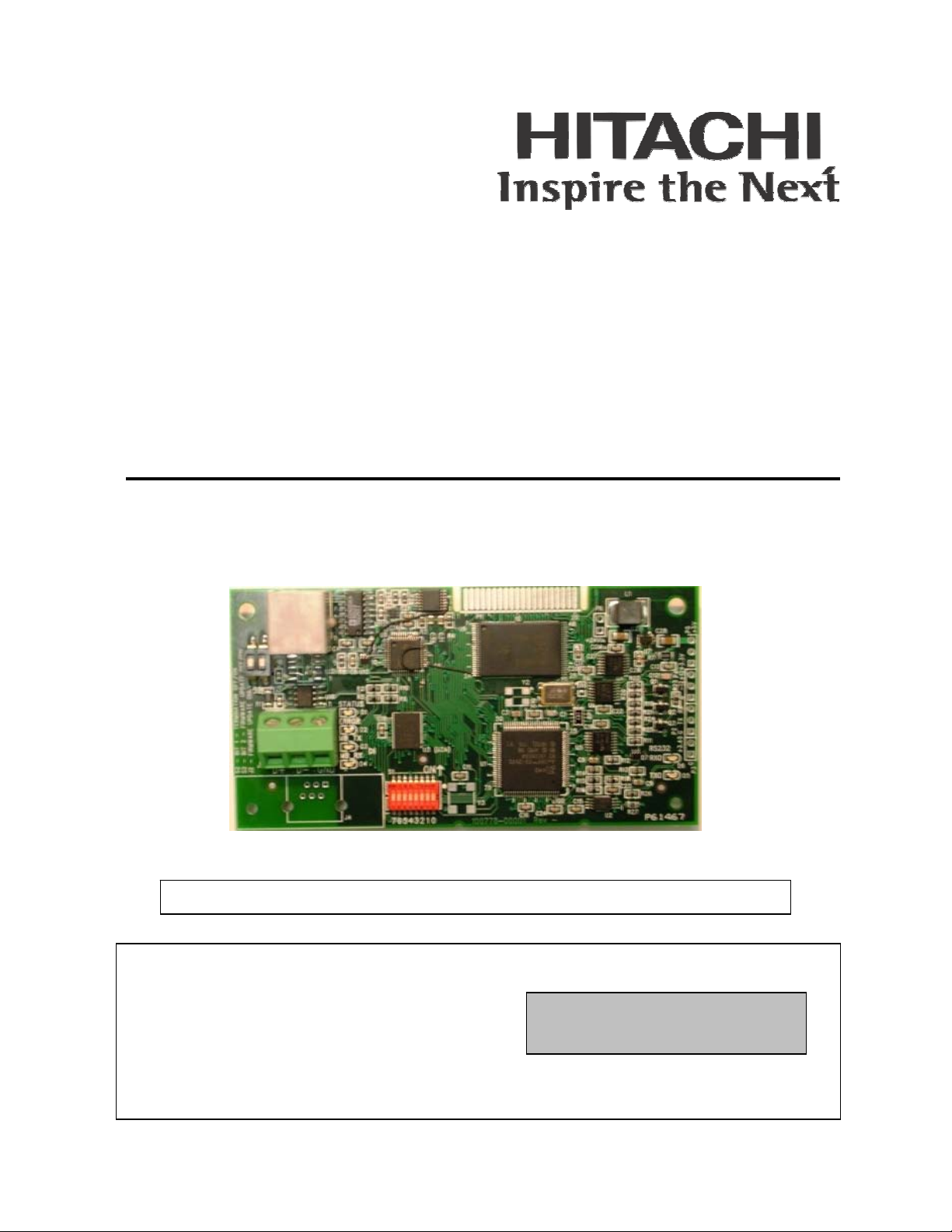
Carton Contents
(1) SJ-MB Modbus Communication Interface Board
(2) Screws to secure board to inverter case (M3 x 8mm)
(1) CD-ROM containing this manual (pdf)
WARRANTY
The warranty period under normal installation and handling conditions shall be eighteen (18) months
from the date of purchase, or twelve (12) months from the date of installation, whichever occurs first.
The warranty shall cover repair or replacement, at Hitachi’s sole discretion, of the SJ-MB Option board.
Service in the following cases, even within the warranty period, shall be to the customers account:
1. Malfunction or damage caused by misuse, modification or unauthorized repair.
2. Malfunction or damage caused by mishandling, dropping, etc., after delivery.
3. Malfunction or damage caused by fire, earthquake, flood, lightning, abnormal input voltage,
contamination, or other natural disasters.
If service is required for the product at your worksite, all expenses associated with field repair are the
purchaser’s responsibility. This warranty only covers service at Hitachi designated service facilities.
If making a warranty claims in reference to the above, please contact the distributor from whom you
purchased the SJ-MB, and provide the model number, purchase date, installation date, and description
of damage or missing components.
Page 5 of 36
Page 6

SAFETY PRECAUTIONS
HIGH VOLTAGE: This symbol indicates high voltage. It calls your attention to items or operations
that could be dangerous to you and other persons operating this equipment. Read the message and
follow the instructions carefully.
WARNING: Indicates a potentially hazardous situation that, if not avoided, can result in serious
injury or death.
CAUTION: Indicates a potentially hazardous situation that, if not avoided, can result in minor to
moderate injury, or serious damage to the product. The situation described in the CAUTION may, if
not avoided, lead to serious results. Important safety measures are described in CAUTION (as well as
WARNING), so be sure to observe them.
HIGH VOLTAGE: Motor control equipment and electronic controllers are connected to hazardous
line voltages. When servicing drives and electronic controllers, there may be exposed components
with housings or protrusions at or above line potential. Extreme care should be taken to protect
against shock. Stand on an insulating pad and make it a habit to use only one hand when checking
components. Always work with another person in case an emergency occurs. Disconnect power
before checking controllers or performing maintenance. Be sure equipment is properly grounded.
Wear safety glasses whenever working on electronic controllers or rotating machinery.
WARNING: This equipment should be installed, adjusted, and serviced by qualified electrical
maintenance personnel familiar with the construction and operation of the equipment and the hazards
involved. Failure to observe this precaution could result in bodily injury.
WARNING: HAZARD OF ELECTRICAL SHOCK. DISCONNECT INCOMING POWER
BEFORE WORKING ON THIS CONTROL.
WARNING: Wait at least five (5) minutes after turning OFF the input power supply before
performing maintenance or an inspection. Otherwise, there is the danger of electric shock.
WARNING: Do not install or remove the SJ-MB Modbus option board while the inverter is
energized. Otherwise there is the danger of electric shock and/or injury due to unexpected inverter
operation.
WARNING: Never modify the unit. Otherwise, there is a danger of electric shock and/or injury.
CAUTION: Be sure to secure the SJ-MB option board with the supplied mounting screws. Make sure
all connections are made securely; otherwise there is danger of a loose connection and unpredictable
operation.
CAUTION: Alarm connection may contain hazardous live voltage even when inverter is
disconnected. When removing the front cover for maintenance or inspection, confirm that incoming
power for alarm connection is completely disconnected.
Chapter 1
Page 6 of 36
Page 7

Chapter 1
CAUTION: Be sure not to touch the surface or terminals of the SJ-MB Modbus option board while
the inverter is energized; otherwise there is the danger of electric shock.
CAUTION: The software lock modes described in the SJ300 inverter manual are NOT supported via
the SJ-MB option board. This means that network commands can bypass any software lock settings
configured via the inverter keypad. It is therefore incumbent on the user to make sure no safety
lockouts are violated through network commands.
CAUTION: When configuring parameters with the standard keypad, the inverter checks for and
inhibits invalid parameter combinations when the STR key is pressed. The SJ-MB bypasses this
check, so it is incumbent on the user to make sure invalid configuration parameters or combinations
are not sent through network commands. Otherwise undesirable inverter behavior may occur.
CAUTION: Certain parameter data ranges vary depending on model and capacity. The SJ-MB does
NOT check to make sure these data are within range. Thus it is incumbent on the user to make sure
data for these parameters is within range for the specific model and rating. These parameters are noted
in the parameter tables in the Appendix. Otherwise undesirable inverter behavior may occur.
INVERTER COMPATIBILITY
The inverter firmware revision number is embedded within the inverter Manufacturing Number, which can be
found on the product nameplate. The SJ-MB Modbus Interface option board is compatible only with SJ300 and
L300P series inverters with Revision Numbers HIGHER than those shown below.
XX
8KT XXXXX XXXXX – for SJ300-xxxXFU 0.4 kW (0.5 hp) to 55 kW (75 hp), or
L300P-xxxXFU or L300P-xxxXBRM 1.5 kW (2 hp) to 75 kW (100 hp)
EMT XXXXX XXXXX – for SJ300-xxxXFU 75kW (100 hp) to 150 kW (200 hp), or
XX
L300P-xxxXFU or L300P-xxxXBRM 90 kW
(125 hp) to 132 kW (175 hp)
Note: All inverters in the model number series L300P-xxxXFU2 are compatible with
the SJ-MB, regardless of revision number. All SJ300 and L300P models
manufactured in 2004 or later are compatible as well.
Page 7 of 36
Page 8

NOTES:
Chapter 1
Page 8 of 36
Page 9
(
)
Chapter 2
Chapter 2 – Installation and Wiring
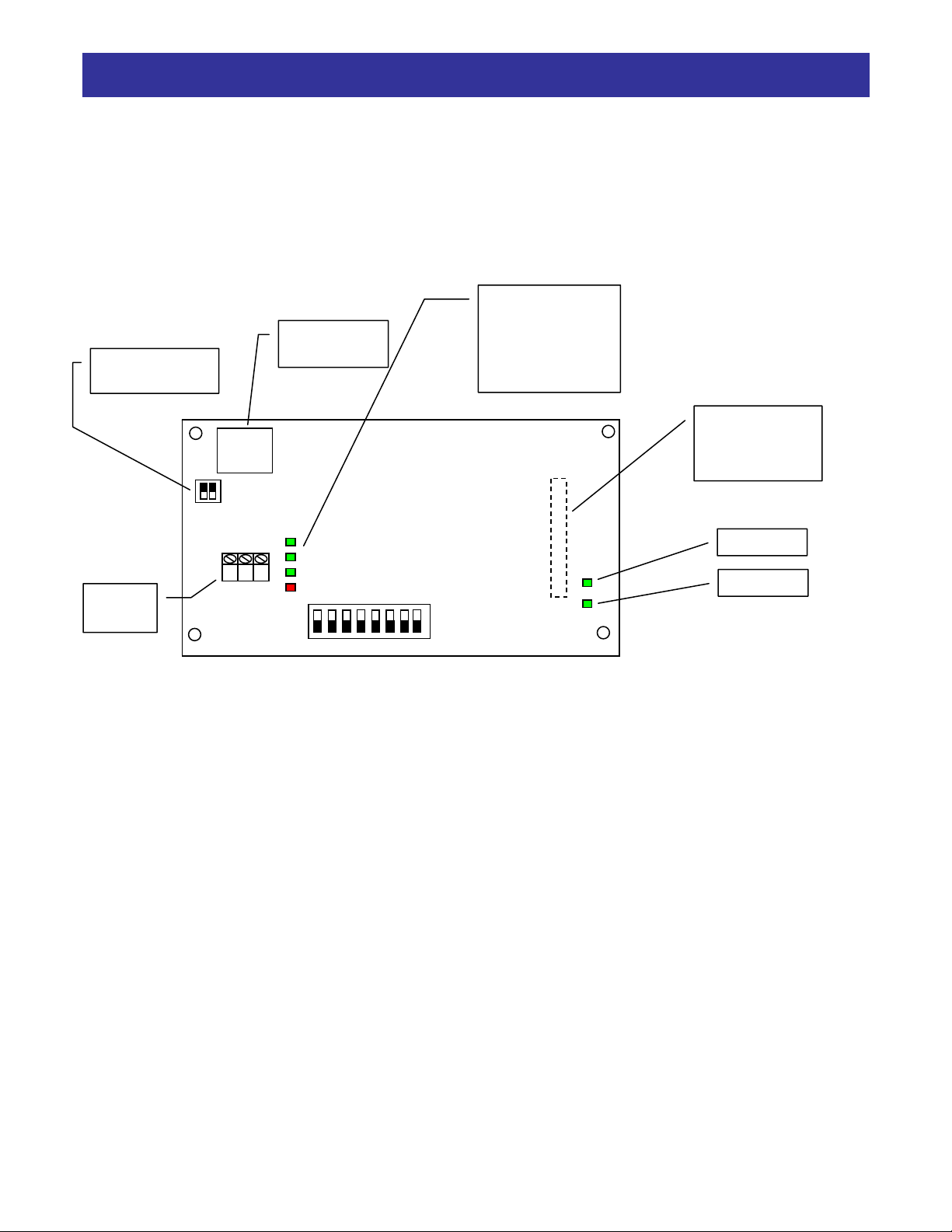
Orientation to Product Features
Figure 2-1 below shows the physical layout of the SJ-MB Modbus option board. In particular, note the location
of status LEDs and DIP-switches.
Left: Termination
Right: Config
Programming
Port
RJ1 1
Jack
Modbus
Port
D+ D- GND
7 6 5 4 3 2 1 0
ON
OFF
Figure 2-1
SJ-MB Layout
Installing the Option Board
Power down the inverter and wait at least five minutes before moving to the next step. Open and remove the
lower terminal cover. Confirm that the red CHARGE LED is extinguished and that the DC bus is fully
discharged before proceeding further, otherwise there is the danger of electric shock. Then remove keypad from
the inverter. You can now remove the upper front cover to expose the two option ports inside.
Figure 2-2 on the next page shows how to install the option board to option port 1 or 2 of the inverter. There are
four holes on the corners of the option board. Align the board with the port connector in the proper orientation
(to the left, when facing the inverter as show). Then align the top two holes with the two screw holes, and the
bottom two holes with the two guide posts. Insert the board fully into the connector. Secure the board with the
two M3 screws supplied.
STATUS LEDs
• STATUS
• ERROR
• TX
• RX
Connector to
connect to
SJ300 or L300P
rear of board
RXD LED
TXD LED
DIP Switches
Page 9 of 36
Page 10
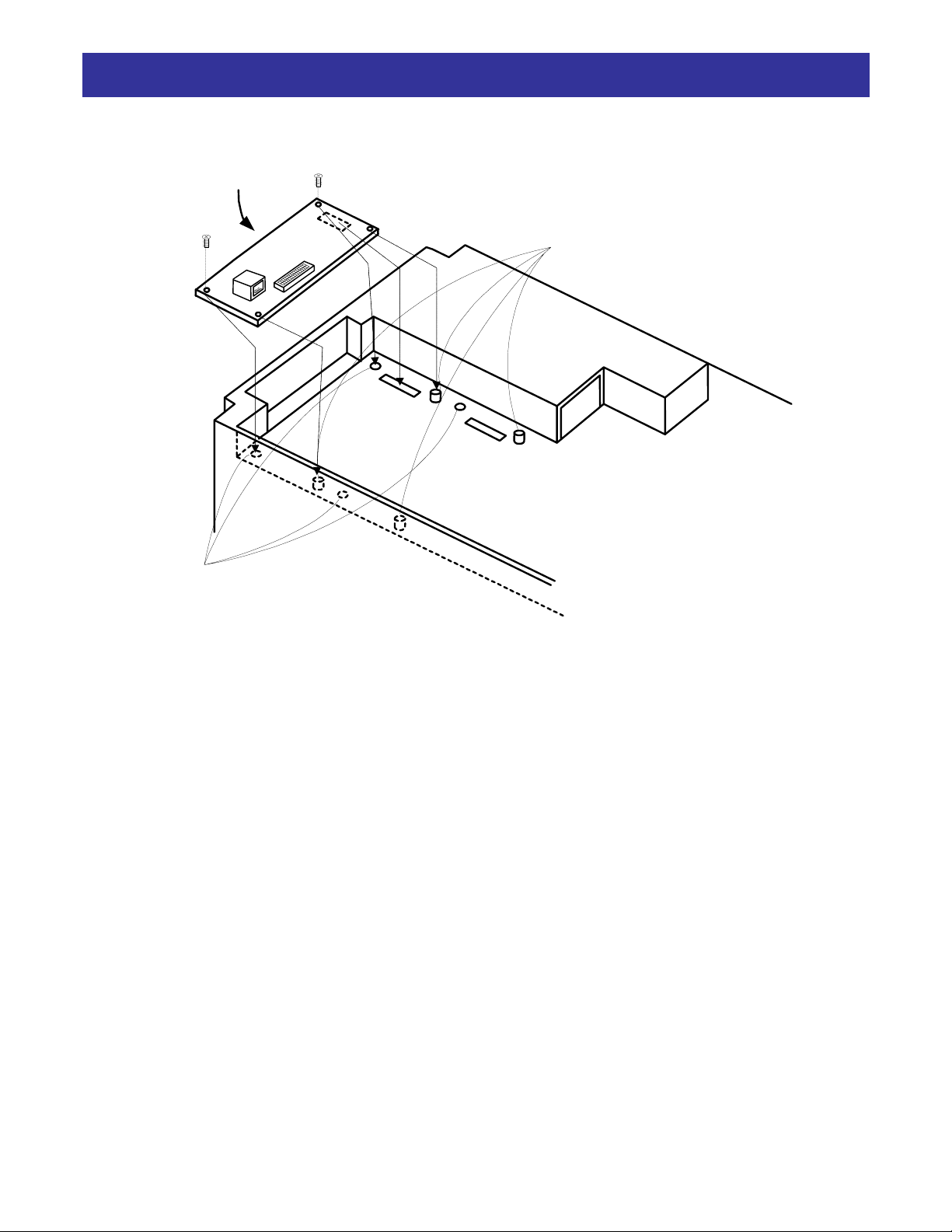
Screw holes for securing the option board
Option board
Option port 1
(M3 screws x 2)
Chapter 2
Guide posts for
option board positioning
Option port 2
Figure 2-2
Installation of SJ-MB
Page 10 of 36
Page 11

Chapter 2
User Interface
The SJ-MB has six LEDs to convey module status and activity.
Four LEDs next to the Modbus port connector:
• STATUS (GREEN) – This LED will be ON whenever the SJ-MB is receiving proper power from the
inverter and the self diagnostics have shown the board to be functioning normally.
• ERROR (RED) – This LED will be ON if the SJ-MB has failed due to a hardware watchdog timeout, or
the Modbus communications has been absent for the software watchdog timeout period.
MB TX – This LED is ON when the SJ-MB is transmitting Modbus data over the network.
•
• MB RX – This LED is ON when the SJ-MB is receiving Modbus data over the network.
Two LEDs near the right edge of the board:
• TXD – This LED indicates communication from the SJ-MB to the inverter through the option port.
• RXD – This LED indicates communication to the SJ-MB from the inverter through the option port.
(These two LEDs may appear blinking or may appear steady ON due to the high blink rate.)
Page 11 of 36
Page 12

NOTES:
Chapter 2
Page 12 of 36
Page 13

Chapter 3
Chapter 3 – Configuration
Configuration of the SJ-MB Board
Ensure that the SJ-MB is properly installed as described in Chapter 2.
There are two DIP-switch banks on the SJ-MB board (see Figure 2-1). The eight-position bank is not used;
however ensure that all switches are in the OFF position.
On the two-position DIP-switch bank, the left switch (bit 1) of controls whether a termination resistor is
connected across the D+ and D- data terminals. This switch should be in the OFF position, unless this SJ-MB
board is the last device in the Modbus/RTU network. In this case, move this switch to the on position to provide
proper network termination resistance. The right switch SHOULD NOT be used. It is for factory use only, and
should be in the OFF position for normal operation.
Make sure that all wiring is secure in the inverter, and that the power connections are free and clear. Be sure to
separate power wiring from control wiring. If they have to cross, be sure that they cross at a right angle to
minimize the possibility of interference. Power up the inverter, and observe the LEDs on the SJ-MB board. The
STATUS LED should be illuminated, and the RX and TX LEDs should blink when Modbus data is being
passed. The red ERROR LED should NOT be illuminated. Also, the RXD and TXD LEDs should be blinking
(may appear as though ON continuously, due to high blink rate). See Chapter 4 for detailed description of LED
functions. If the LED conditions are not correct, proceed to Chapter 5 for Troubleshooting. If you power up the
inverter before powering up the PC, an error code may appear. After powering up the PC and properly
connecting the cable, you should be able to clear the error with the STOP/RESET key on the inverter keypad.
If the LEDs are correct, continue with the configuration.
Configuring Parameters that Control the SJ-MB
Using either the keypad, or the ProDrive Programming Software, you will need to configure the communication
settings for the SJ-MB board. Refer to the following table.
Function
Code
Name Description
Run
Mode
Edit
Lo Hi
–FE
(EU)
Defaults
–FU
(US)
–FR
(Jpn)
Setting for Modbus Control
via SJ-MB
C070
Data
Command
Method
Four options; select codes:
02 Digital Operator
03 RS485 port
04 Expansion board 1
05 Expansion board 2
8 8
02 02 02 02
Page 13 of 36
Page 14

C071
Comm.
Speed
Selection
Five options; select codes:
02 Test
03 2400 bps
04 4800 bps
05 9600 bps
06 19200 bps
8 9
Chapter 3
04 04 04 To Match Master Device
C072
C073
C074
C075
C078
Node
Allocation
Comm. Data
Length
Selection
Comm.
Parity
Selection
Comm. Stop
Bit Selection
Comm. W ait
Time
Set the desired address of the
inverter on the Modbus/RTU
network. Range is 1 to 32.
Two options, select codes:
07 7-bit data
08 8-bit data
Three options, select codes:
00 No parity
01 Even parity
02 Odd parity
Two options, select codes:
01 1 stop bit
02 2 stop bits
Time the board waits after
receiving a message before it
transmits data. Range is 0.0 to
1000 ms
8 9
8 9
8 9
8 9
8 9
1 1 1 As required
7 7 7 To Match Master Device
00 00 00 To Match Master Device
1 1 1 To Match Master Device
0.0 0.0 0.0 As required
Page 14 of 36
Page 15

Chapter 4
Chapter 4 – Operation
Setting Up the Inverter for Modbus Network Operation
Once the SJ-MB board has been properly configured and connected to a network as described in Chapter 3, it is
capable of reading data from and writing data to the inverter. However if it is desired to have either the RUN
command and/or the speed reference come from the Ethernet master, you must change two inverter parameters
as shown in the following table.
Run
Function
Code
A001
A002
Name Description
Six options; select codes:
00 Keypad potentiometer
Frequency
Source
Setting
Run
command
source setting
01Control terminal
02 Function F001 setting
03 RS485 serial command
04 Expansion board 1
05 Expansion board 2
Five options; select codes:
01 Input terminal [FW] or [RV]
(assignable)
02 Run key on keypad, or
digital operator
03 RS485 serial command
04 Start/Stop, expansion card #1
05 Start/Stop, expansion card #2
Mode
Edit
Lo Hi
8 8
8 8
Supported MODBUS Functions
The SJ-MB is implemented with the MODBUS/RTU communication protocol. It supports the following
MODBUS functions:
• 1 - MODBUS_READ_COILS (up to 32 at a time)
• 3 - MODBUS_READ_MULTIPLE_REGS (Up to 4 at a time)
• 5 - MODBUS_WRITE_COIL
• 6 - MODBUS_WRITE_SINGLE_REGISTER
• 8 - MODBUS_LOOPBACK_TEST
• 15 - MODBUS_FORCE_MULTIPLE_COILS (up to 32 at a time)
• 16 - MODBUS_WRITE_MULTIPLE_REGS (up to 4 at a time)
Additional MODBUS/RTU protocol details, including specifications, application information, implementation
guides, and other resources are available from the web site
www.modbus.org.
Defaults
–FE
(EU)
01 01 02 02
01 01 02 02
–FU
(US)
–FR
(Jpn)
Setting for Modbus Control
Page 15 of 36
Page 16

NOTES:
Chapter 4
Page 16 of 36
Page 17

Chapter 5
Chapter 5 – Troubleshooting
In general, the first step to troubleshooting should be to inspect the status LEDs on the SJ-MB board, in addition
to the inverter operator/keypad display. These will give valuable clues to the nature of the problem.
In addition, the inverter operator/keypad will provide diagnostic information for certain types of errors. Error
codes for the option boards will have the format of:
E6X.X for a board installed in option slot 1, or E7X.X for a board installed in option slot 2. The number
to the right of the decimal point indicates the drive status at the time of trip, as follows:
During
deceleration
EXX.0
At reset
EXX.1
At stop
EXX.2
At constant
EXX.3
EXX.6
The digit immediately to the left of the decimal point has the following meaning:
Code Trip Name Cause Check Remedy
EX0.X
speed
At starting
Modbus Communication
Error
EXX.4
EXX.7
Defective
connection
PC not powered up
or not connected to
inverter
Network
configuration error
During
acceleration
During DC
injection
braking
EXX.5
EXX.8
Connectors (plugs
& jacks), cable
That PC is powered
on and connected
Verify proper
Modbus setup of
SJ-MB and master
device
f0 Stop
During overload
restriction
Replace or repair;
press STOP/RESET
on inverter keypad
Press STOP/RESET
on inverter keypad
Reconfigure
incorrect settings.
EX9.X
Internal Communication
Error (between SJ-MB and
inverter)
Inverter Mismatch
(blinking display as
shown)
Option board ajar o
loose
Board lockup Check status LEDs
Board defective Check status LEDs Replace SJ-MB
Inverter firmware
version not
compatible with
SJ-MB option
board
Page 17 of 36
Verify board is
r
properly seated in
connector
Inverter
Manufacturing
Number for version
(see Page 7)
Remove and reseat
board
Press STOP/RESET
key on inverter or
cycle power
Replace Inverter
with later version
Page 18

NOTES:
Appendix
Page 18 of 36
Page 19

Appendix
Appendix – Parameter List
The following lists include the combined parameter sets of both the L300P series and SJ300 series of inverters.
Therefore, all parameters listed are not available on both series. Please refer to the instruction manual for the
inverter you have to determine the list of available parameters. Then you can find the parameter on these lists
and determine proper addressing for Modbus/RTU.
Coil List
Coil
No.
0001h Operation command R/W 1: Run, 0: Stop (valid when A002 = 02)
0002h Rotation direction command R/W 1: Reverse, 0 : Forward (valid when A002 = 02)
0003h External trip (EXT) R/W 1: Trip
0004h Trip reset (RS) R/W 1: Reset
0007h Intelligent input terminal [1] R/W 1: ON, 0: OFF (*1)
0008h Intelligent input terminal [2] R/W 1: ON, 0: OFF (*1)
0009h Intelligent input terminal [3] R/W 1: ON, 0: OFF (*1)
000Ah Intelligent input terminal [4] R/W 1: ON, 0: OFF (*1)
000Bh Intelligent input terminal [5] R/W 1: ON, 0: OFF (*1)
000Ch Intelligent input terminal [6] R/W 1: ON, 0: OFF (*1)
000Dh Intelligent input terminal [7] R/W 1: ON, 0: OFF (*1)
000Eh Intelligent input terminal [8] R/W 1: ON, 0: OFF (*1)
000Fh Operation status R 1: Run, 0: Stop (interlocked to "d003")
0010h Rotation direction R
0013h RUN (running) R 1: Tripped, 0: Normal
0014h FA1 (constant-speed reached) R 1: ON, 0: OFF
0015h FA2 (set frequency overreached) R 1: ON, 0: OFF
0016h
0017h OD (output deviation for PID control) R 1: ON, 0: OFF
0018h AL (alarm signal) R 1: ON, 0: OFF
0019h FA3 (set frequency reached) R 1: ON, 0: OFF
001Ah OTQ (over-torque) R 1: ON, 0: OFF
001Bh IP (instantaneous power failure) R 1: ON, 0: OFF
001Ch UV (under voltage) R 1: ON, 0: OFF
001Dh TRQ (torque limited) R 1: ON, 0: OFF
001Eh RNT (operation time over) R 1: ON, 0: OFF
001Fh ONT (plug-in time over) R 1: ON, 0: OFF
0020h THM (thermal alarm signal) R 1: ON, 0: OFF
0026h BRK (brake release) R 1: ON, 0: OFF
0027h BER (brake error) R 1: ON, 0: OFF
0028h ZS (0 Hz detection signal) R 1: ON, 0: OFF
0029h DSE (speed deviation maximum) R 1: ON, 0: OFF
002Ah POK (positioning completed) R 1: ON, 0: OFF
OL (overload notice advance signal
(1))
Item R/W Setting
1: Reverse rotation, 0: Forward rotation (interlocked to
"d003")
R 1: ON, 0: OFF
Page 19 of 36
Page 20

Appendix
002Bh FA4 (set frequency overreached 2) R 1: ON, 0: OFF
002Ch FA5 (set frequency reached 2) R 1: ON, 0: OFF
002Dh
0032h FBV (PID feedback comparison) R 1: ON, 0: OFF
0033h
0034h LOG1 (logical operation result 1) R 1: ON, 0: OFF
0035h LOG2 (logical operation result 2) R 1: ON, 0: OFF
0036h LOG3 (logical operation result 3) R 1: ON, 0: OFF
0037h LOG4 (logical operation result 4) R 1: ON, 0: OFF
0038h LOG5 (logical operation result 5) R 1: ON, 0: OFF
0039h LOG6 (logical operation result 6) R 1: ON, 0: OFF
003Ah WAC (capacitor life warning) R 1: ON, 0: OFF
003Bh WAF (cooling-fan speed drop) R 1: ON, 0: OFF
003Ch FR (starting contact signal) R 1: ON, 0: OFF
003Dh OHF (heat sink overheat warning) R 1: ON, 0: OFF
003Eh LOC (low-current indication signal) R 1: ON, 0: OFF
003Fh M01 (general output 1) R 1: ON, 0: OFF
0040h M02 (general output 2) R 1: ON, 0: OFF
0041h M03 (general output 3) R 1: ON, 0: OFF
0042h M04 (general output 4) R 1: ON, 0: OFF
0043h M05 (general output 5) R 1: ON, 0: OFF
0044h M06 (general output 6) R 1: ON, 0: OFF
0046h FWR (forward rotation) R 1: ON, 0: OFF
0047h RVR (reverse rotation) R 1: ON, 0: OFF
0048h MJA (major failure) R 1: ON, 0: OFF
0049h Data writing in progress R 1: Writing in progress, 0: Normal status
004Ah CRC error R 1: Error detected, 0: No error (*2)
004Bh Overrun R 1: Error detected, 0: No error (*2)
004Ch Framing error R 1: Error detected, 0: No error (*2)
004Dh Parity error R 1: Error detected, 0: No error (*2)
004Eh Sum check error R 1: Error detected, 0: No error (*2)
*1 Normally, this coil is turned on when the corresponding intelligent input terminal on the control circuit terminal
*2 Communication error data is retained until an error reset command is input (can be reset during inverter
OL2 (overload notice advance signal
(2))
NDc (communication line
disconnection)
block is turned on or the coil itself is set to on. In this regard, the operation of the intelligent input terminal has
priority over the operation of the coil. If disconnection of the communication line has disabled the master
system from turning off the coil, turn the corresponding intelligent input terminal on the control circuit block on
and off. This operation turns off the coil.
operation.)
R 1: ON, 0: OFF
R 1: ON, 0: OFF
Page 20 of 36
Page 21

Appendix
Register List
Dec Hex Description
1 0x1 Set frequency (Hz) / PID Setpoint (%) [MSW] F1
2 0x2 Set frequency (Hz) / PID Setpoint (%) [LSW] F1
3 0x3 Status of Inverter [BYTE 3] R1
4 0x4 Status of Inverter [BYTE 2] R1
5 0x5 Status of Inverter [BYTE 1] R1
17 0x11 Accumulated number of Trip(error) D80
18 0x12 Factor and Status of Trip1 [MSW] D81
19 0x13 Factor and Status of Trip1 [LSW] D81
20 0x14 Frequency of Trip1 [MSW]
21 0x15 Frequency of Trip1 [LSW]
22 0x16 Output current of Trip1
23 0x17 PN voltage (DC voltage) of Trip1
24 0x18 Accumulated time during running of Trip1 [MSW]
25 0x19 Accumulated time during running of Trip1 [LSW]
26 0x1A Accumulated time during power ON of Trip1 [MSW]
27 0x1B Accumulated time during power ON of Trip1 [LSW]
28 0x1C Factor and Status of Trip2 [MSW] D82
29 0x1D Factor and Status of Trip2 [LSW] D82
30 0x1E Frequency of Trip2 [MSW]
31 0x1F Frequency of Trip2 [LSW]
32 0x20 Output current of Trip2
33 0x21 PN voltage (DC voltage) of Trip2
34 0x22 Accumulated time during running of Trip2 [MSW]
35 0x23 Accumulated time during running of Trip2 [LSW]
36 0x24 Accumulated time during power ON of Trip2 [MSW]
37 0x25 Accumulated time during power ON of Trip2 [LSW]
38 0x26 Factor and Status of Trip3 [MSW] D83
39 0x27 Factor and Status of Trip3 [LSW] D83
40 0x28 Frequency of Trip3 [MSW]
41 0x29 Frequency of Trip3 [LSW]
42 0x2A Output current of Trip3
43 0x2B PN voltage (DC voltage) of Trip3
44 0x2C Accumulated time during running of Trip3 [MSW]
45 0x2D Accumulated time during running of Trip3 [LSW]
46 0x2E Accumulated time during power ON of Trip3 [MSW]
47 0x2F Accumulated time during power ON of Trip3 [LSW]
48 0x30 Factor and Status of Trip4 [MSW] D84
49 0x31 Factor and Status of Trip4 [LSW] D84
50 0x32 Frequency of Trip4 [MSW]
51 0x33 Frequency of Trip4 [LSW]
52 0x34 Output current of Trip4
53 0x35 PN voltage (DC voltage) of Trip4
54 0x36 Accumulated time during running of Trip4 [MSW]
55 0x37 Accumulated time during running of Trip4 [LSW]
56 0x38 Accumulated time during power ON of Trip4 [MSW]
Parameter
Inverter
Page 21 of 36
Page 22

Appendix
57 0x39 Accumulated time during power ON of Trip4 [LSW]
58 0x3A Factor and Status of Trip5 [MSW] D85
59 0x3B Factor and Status of Trip5 [LSW] D85
60 0x3C Frequency of Trip5 [MSW]
61 0x3D Frequency of Trip5 [LSW]
62 0x3E Output current of Trip5
63 0x3F PN voltage (DC voltage) of Trip5
64 0x40 Accumulated time during running of Trip5 [MSW]
65 0x41 Accumulated time during running of Trip5 [LSW]
66 0x42 Accumulated time during power ON of Trip5 [MSW]
67 0x43 Accumulated time during power ON of Trip5 [LSW]
68 0x44 Factor and Status of Trip6 [MSW] D86
69 0x45 Factor and Status of Trip6 [LSW] D86
70 0x46 Frequency of Trip6 [MSW]
71 0x47 Frequency of Trip6 [LSW]
72 0x48 Output current of Trip6
73 0x49 PN voltage (DC voltage) of Trip6
74 0x4A Accumulated time during running of Trip6 [MSW]
75 0x4B Accumulated time during running of Trip6 [LSW]
76 0x4C Accumulated time during power ON of Trip6 [MSW]
77 0x4D Accumulated time during power ON of Trip6 [LSW]
2304 0x900 Writing to EEPROM
4097 0x1001 Output frequency [MSW] D1
4098 0x1002 Output frequency [LSW] D1
4099 0x1003 Output current D2
4100 0x1004 Direction of p resent running D3
4101 0x1005 Feedback data of PID control [MSW] D4
4102 0x1006 Feedback data of PID control [LSW] D4
4103 0x1007 Status of Input terminal D5
4104 0x1008 Status of output terminal D6
4105 0x1009 Value of conversion of frequency [MSW] D7
4106 0x100A Value of conversion of frequency [LSW] D7
4112 0x1010 Output Torque D12
4113 0x1011 Output voltage D13
4114 0x1012 Input electric power D14
4117 0x1015 Accumulate d time during running [MSW] D16
4118 0x1016 Accumulate d time during running [LSW] D16
4119 0x1017 Accumulate d time during Power ON [MSW] D17
4120 0x1018 Accumulate d time during Power ON [LSW] D17
4134 0x1026 DC Voltage D102
4135 0x1027 On time of BRD running D103
4136 0x1028 Used rate of electroni cs thermal protection D104
4355 0x1103 1st Acceleration time 1 [MSW] F2
4356 0x1104 1st Acceleration time 1 [LSW] F2
4357 0x1105 1st Decel eration time 1 [MSW] F3
Page 22 of 36
Page 23

Appendix
4358 0x1106 1st Decel eration time 1 [LSW] F3
4359 0x1107 Selection of running direction for DIG-OPE F4
4609 0x1201 Selection of frequency com mand destination A1
4610 0x1202 Selection of running com mand destination A2
4611 0x1203 1st Base frequency A3
4612 0x1204 1st Maximum frequen cy A4
4613 0x1205 Selection of AT function A5
4614 0x1206 Selection of O2 terminal function A6
4619 0x120B Start frequen cy of .O. terminal [MSW] A11
4620 0x120C Start frequency of .O. terminal [LSW] A11
4621 0x120D End frequency of .O. terminal [MSW] A12
4622 0x120E End frequency of .O. terminal [LSW] A12
4623 0x120F Starting rate of O terminal A13
4624 0x1210 End rate of O terminal A14
4625 0x1211 Selection of starting function of O terminal A15
4626 0x1212 Sampling number of fetching data from .O. A16
4629 0x1215 Selection of Multispeed method A19
4630 0x1216 1st setting Multispeed frequency 0 [MSW] A20
4631 0x1217 1st setting Multispeed frequency 0 [LSW] A20
4632 0x1218 Multispeed frequency 1 [MSW] A21
4633 0x1219 Multispeed frequency 1 [LSW] A21
4634 0x121A Multispeed frequency 2 [MSW] A22
4635 0x121B Multispeed frequency 2 [LSW] A22
4636 0x121C Multispeed frequency 3 [MSW] A23
4637 0x121D Multispeed frequency 3 [LSW] A23
4638 0x121E Multispeed frequency 4 [MSW] A24
4639 0x121F Multispeed frequency 4 [LSW] A24
4640 0x1220 Multispeed frequency 5 [MSW] A25
4641 0x1221 Multispeed frequency 5 [LSW] A25
4642 0x1222 Multispeed frequency 6 [MSW] A26
4643 0x1223 Multispeed frequency 6 [LSW] A26
4644 0x1224 Multispeed frequency 7 [MSW] A27
4645 0x1225 Multispeed frequency 7 [LSW] A27
4646 0x1226 Multispeed frequency 8 [MSW] A28
4647 0x1227 Multispeed frequency 8 [LSW] A28
4648 0x1228 Multispeed frequency 9 [MSW] A29
4649 0x1229 Multispeed frequency 9 [LSW] A29
4650 0x122A Multispeed frequency 10 [MSW] A30
4651 0x122B Multispeed frequency 10 [LSW] A30
4652 0x122C Multispeed frequency 11 [MSW] A31
4653 0x122D Multispeed frequency 11 [LSW] A31
4654 0x122E Multispeed frequency 12 [MSW] A32
4655 0x122F Multispeed frequency 12 [LSW] A32
4656 0x1230 Multispeed frequency 13 [MSW] A33
4657 0x1231 Multispeed frequency 13 [LSW] A33
4658 0x1232 Multispeed frequency 14 [MSW] A34
4659 0x1233 Multispeed frequency 14 [LSW] A34
4660 0x1234 Multispeed frequency 15 [MSW] A35
Page 23 of 36
Page 24

Appendix
4661 0x1235 Multispeed frequency 15 [LSW] A35
4664 0x1238 Jogging frequency A38
4665 0x1239 Selection of Jogging method A39
4667 0x123B Selection of 1st Torque boost Method A41
4668 0x123C Value of 1st Manual torque boost A42
4669 0x123D 1st Break point of manual torque boost A43
4670 0x123E Selection of 1st Control method A44
4671 0x123F Gain of output voltage A45
4677 0x1245 Selection of DC braking method A51
4678 0x1246 Frequency of DC braking start A52
4679 0x1247 Delay time of DC braking start A53
4680 0x1248 Power of DC braking(end of running) A54
4681 0x1249 Time of DC braking working A55
4682 0x124A Selection of edge/level action of DC braking trigger A56
4683 0x124B Power of DC braking (start of running) A57
4684 0x124C Time of DC braking working for beginning of inverter running A58
4685 0x124D Carrier frequency of DC braking A59
4687 0x124F 1st Upper limiter frequency [MSW] A61
4688 0x1250 1st Upper limiter frequency [LSW] A61
4689 0x1251 1st Lower limiter frequency [MSW] A62
4690 0x1252 1st Lower limiter frequency [LSW] A62
4691 0x1253 Jumping frequency 1 [MSW] A63
4692 0x1254 Jumping frequency 1 [LSW] A63
4693 0x1255 Width of jumping frequency 1 A64
4694 0x1256 Jumping frequency 2 [MSW] A65
4695 0x1257 Jumping frequency 2 [LSW] A65
4696 0x1258 Width of jumping frequency 2 A66
4697 0x1259 Jumping frequency 3 [MSW] A67
4698 0x125A Jumping frequency 3 [LSW] A67
4699 0x125B Width of jumping frequency 3 A68
4700 0x125C Frequency of stopping acceleration [MSW] A69
4701 0x125D Frequency of stopping acceleration [LSW] A69
4702 0x125E Time of stopping to accelerate A70
4703 0x125F Selection of PID control presence A71
4704 0x1260 Proportional(P) gain of PID control A72
4705 0x1261 Integrate (I) gain of PID control A73
4706 0x1262 Differential (D) gain of PID control A74
4707 0x1263 Scale of PID control A75
4708 0x1264 Selection of feedback destination for PID control A76
4713 0x1269 Selection of AVR function A81
4714 0x126A Selection of Motor voltage A82
4717 0x126D Selection of operation mode A85
4718 0x126E Response time of Energy saving function A86
4724 0x1274 1st Acceleration time 2 [MSW] A92
Page 24 of 36
Page 25

Appendix
4725 0x1275 1st Acceleration time 2 [LSW] A92
4726 0x1276 1st Deceleration time 2 [MSW] A93
4727 0x1277 1st Deceleration time 2 [LSW] A93
4728 0x1278 Selection of 1st 2-stage accel/decel Method A94
4729 0x1279 1st Frequency of 2-stage acceleration [MSW] A95
4730 0x127A 1st Frequency of 2-stage acceleration [LSW] A95
4731 0x127B 1st Frequency of 2-stage deceleration [MSW] A96
4732 0x127C 1st Frequency of 2-stage deceleration [LSW] A96
4733 0x127D Selection of acceleration pattern A97
4734 0x127E Selection of deceleration pattern A98
4737 0x1281 Start frequency of .OI. terminal [MSW] A101
4738 0x1282 Start frequency of .OI. terminal [LSW] A101
4739 0x1283 End frequency of .OI. terminal [MSW] A102
4740 0x1284 End frequency of .OI. terminal [LSW] A102
4741 0x1285 Starting rate of OI terminal A103
4742 0x1286 End rate of OI terminal A104
4743 0x1287 Selection of starting function of OI terminal A105
4749 0x128D Start frequency of .O2. terminal [MSW] A111
4750 0x128E Start frequency of .O2. terminal [LSW] A111
4751 0x128F End frequency of .O2. terminal [MSW] A112
4752 0x1290 End frequency of .O2. terminal [LSW] A112
4753 0x1291 Starting rate of O2 terminal A113
4754 0x1292 End rate of O2 terminal A114
4773 0x12A5 Curve constant of acceleration A131
4774 0x12A6 Curve constant of deceleration A132
4865 0x1301 Selection of retry method B1
4866 0x1302 Acceptable time for Instantaneous power failure B2
4867 0x1303 Waiting time of retry B3
4868 0x1304 Selection of method(action) at instantaneous power and under voltage B4
4869 0x1305 Retry number of instantaneous power and under voltage B5
4870 0x1306 Selection of fail phase function B6
4871 0x1307 Frequency of frequency matching [MSW] B7
4872 0x1308 Frequency of frequency matching [LSW] B7
4877 0x130D Level of 1st Electronic thermal protection B12
4878 0x130E Selection of characteristic of 1st electronic thermal protection B13
4880 0x1310 Free electronic thermal frequency 1 B15
4881 0x1311 Free electronic thermal current 1 B16
4882 0x1312 Free electronic thermal frequency 2 B17
4883 0x1313 Free electronic thermal current 2 B18
4884 0x1314 Free electronic thermal frequency 3 B19
4885 0x1315 Free electronic thermal current 3 B20
4886 0x1316 Selection of method of overload restriction1 B21
4887 0x1317 Level of Overload restriction 1 B22
Page 25 of 36
Page 26

Appendix
4888 0x1318 Constant value of Overload restriction 1 B23
4889 0x1319 Selection of method of overload restriction 2 B24
4890 0x131A Level of Overload restriction 2 B25
4891 0x131B Constant value of Overload restriction 2 B26
4896 0x1320 Selection of method of Software lock B31
4899 0x1323 Display time of warning [MSW] B34
4900 0x1324 Display time of warning [LSW] B34
4901 0x1325 Selection of running direction limitation B35
4902 0x1326 Selection of method of reducing voltage start B36
4903 0x1327 Selection of Display B37
4906 0x132A Selection of method of Torque limiter B40
4907 0x132B Level of torque limiter in forward and drive (1st quadrant) B41
4908 0x132C Level of torque limiter in reverse and regenerative (2nd quadrant) B42
4909 0x132D Level of torque limiter in reverse and drive (3rd quadrant) B43
4910 0x132E Level of torque limiter in forward and regenerative (4th quadrant) B44
4911 0x132F Selection of LAD stop by torque B45
4912 0x1330 Selection of preventive of reverse running B46
4916 0x1334 Selection of Non stop operation at instantaneous power failure B50
4917 0x1335 Starting voltage of Nonstop operation for Instantaneous power failure B51
Starting voltage of OV-LAD stop at Nonstop operation for Instantaneous power
4918 0x1336
4919 0x1337
4920 0x1338
4921 0x1339
4949 0x1355 Minimum frequency B82
4950 0x1356 Carrier frequency(PWM frequency B83
4951 0x1357 Selection of Initialization B84
4952 0x1358 Selection of initialized data B85
4953 0x1359 Coefficient of converting frequency B86
4954 0x135A Selection of .STOP. key function B87
4955 0x135B Selection free run function B88
4957 0x135D Usage rate of BRD B90
4958 0x135E Selection of action at stop B91
4959 0x135F Selection of action of cooling fan B92
4962 0x1362 Selection of BRD function B95
4963 0x1363 On level of BRD B96
4965 0x1365 Selection of Thermister function B98
4966 0x1366 Level of Thermister error B99
4967 0x1367 Free V/F control frequency 1 B100
4968 0x1368 Free V/F control voltage 1 B101
4969 0x1369 Free V/F control frequency 2 B102
4970 0x136A Free V/F control voltage 2 B103
failure
Deceleration time of Non-stop operation at Instantaneous power failure
[MSW]
Deceleration time of Non-stop operation at Instantaneous power failure
[LSW]
Frequency width of starting deceleration at Nonstop operation for
Instantaneous power failure
B52
B53
B53
B54
Page 26 of 36
Page 27

Appendix
4971 0x136B Free V/F control frequency 3 B104
4972 0x136C Free V/F control voltage 3 B105
4973 0x136D Free V/F control frequency 4 B106
4974 0x136E Free V/F control voltage 4 B107
4975 0x136F Free V/F control frequency 5 B108
4976 0x1370 Free V/F control voltage 5 B109
4977 0x1371 Free V/F control frequency 6 B110
4978 0x1372 Free V/F control voltage 6 B111
4979 0x1373 Free V/F control frequency 7 B112
4980 0x1374 Free V/F control voltage 7 B113
4987 0x137B Selection of external braking function B120
4988 0x137C Waiting time for establishing external braking condition B121
4989 0x137D Waiting time for acceleration at external braking B122
4990 0x137E Waiting time for stop at external braking B123
4991 0x137F Waiting time for confirmation signal at external braking B124
4992 0x1380 Release frequency of external braking B125
4993 0x1381 Release current of external braking B126
5121 0x1401 Selection of function in Intelligent input 1 C1
5122 0x1402 Selection of function in Intelligent input 2 C2
5123 0x1403 Selection of function in Intelligent input 3 C3
5124 0x1404 Selection of function in Intelligent input 4 C4
5125 0x1405 Selection of function in Intelligent input 5 C5
5126 0x1406 Selection of function in Intelligent input 6 C6
5127 0x1407 Selection of function in Intelligent input 7 C7
5128 0x1408 Selection of function in Intelligent input 8 C8
5131 0x140B Selection of a(NO) or b(NC) contact in Intelligent input 1 C11
5132 0x140C Selection of a(NO) or b(NC) contact in Intelligent input 2 C12
5133 0x140D Selection of a(NO) or b(NC) contact in Intelligent input 3 C13
5134 0x140E Selection of a(NO) or b(NC) contact in Intelligent input 4 C14
5135 0x140F Selection of a(NO) or b(NC) contact in Intelligent input 5 C15
5136 0x1410 Selection of a(NO) or b(NC) contact in Intelligent input 6 C16
5137 0x1411 Selection of a(NO) or b(NC) contact in Intelligent input 7 C17
5138 0x1412 Selection of a(NO) or b(NC) contact in Intelligent input 8 C18
5139 0x1413 Selection of a(NO) or b(NC) contact in FW input C19
5141 0x1415 Selection of function in Intelligent output 11 C21
5142 0x1416 Selection of function in Intelligent output 12 C22
5143 0x1417 Selection of function in Intelligent output 13 C23
5144 0x1418 Selection of function in Intelligent output 14 C24
5145 0x1419 Selection of function in Intelligent output 15 C25
5146 0x141A Selection of function in Alarm relay output C26
5147 0x141B Selection of FM function C27
5148 0x141C Selection of AM function C28
5149 0x141D Selection of AMI function C29
5151 0x141F Selection of a(NO) or b(NC) contact in Intelligent output 11 C31
5152 0x1420 Selection of a(NO) or b(NC) contact in Intelligent output 12 C32
5153 0x1421 Selection of a(NO) or b(NC) contact in Intelligent output 13 C33
Page 27 of 36
Page 28

Appendix
5154 0x1422 Selection of a(NO) or b(NC) contact in Intelligent output 14 C34
5155 0x1423 Selection of a(NO) or b(NC) contact in Intelligent output 15 C35
5156 0x1424 Selection of a(NO) or b(NC) contact in Alarm relay output C36
5160 0x1428 Selection of output mode of overload warning signal C40
5161 0x1429 Level1 of overload restriction warning C41
5162 0x142A Arrival frequency at acceleration1 [MSW] C42
5163 0x142B Arrival frequency at acceleration1 [LSW] C42
5164 0x142C Arrival frequency at deceleration1 [MSW] C43
5165 0x142D Arrival frequency at deceleration1 [LSW] C43
5166 0x142E Level over acceptable deviation of PID control C44
5167 0x142F Arrival frequency at acceleration2 [MSW] C45
5168 0x1430 Arrival frequency at acceleration2 [LSW] C45
5169 0x1431 Arrival frequency at deceleration2 [MSW] C46
5170 0x1432 Arrival frequency at deceleration2 [LSW] C46
5179 0x143B Level of over torque in forward and drive (1st quadrant) C55
5180 0x143C Level of over torque in reverse and regenerative (2nd quadrant) C56
5181 0x143D Level of over torque in reverse and drive (3rd quadrant) C57
5182 0x143E Level of over torque in forward and regenerative (4th quadrant) C58
5185 0x1441 Warning Level of electronic thermal protection C61
5186 0x1442 Selection of Alarm code C62
5187 0x1443 Level f detecting Zero speed C63
5195 0x144B Selection of communication speed for RS485 C71
5196 0x144C Selection of Inverter address for RS 485 C72
5197 0x144D Selection of bit length of data for RS485 C73
5198 0x144E Selection of parity (odd or even) for RS485 C74
5199 0x144F Selection of stop bit for RS485 C75
5202 0x1452 Waiting time of communication start C78
5205 0x1455 Adjustment of .O. terminal C81
5206 0x1456 Adjustment of .OI. terminal C82
5207 0x1457 Adjustment of .O2. terminal C83
5209 0x1459 Adjusting value of Thermister C85
5215 0x145F Selection of Debug mode method C91
5225 0x1469 Selection of UP/DOWN function C101
5226 0x146A Selection of RESET function C102
5227 0x146B Selection of frequency matching function at RESET C103
5229 0x146D Adjustment of FM(digital monitor) B81
5230 0x146E Adjustment of AM(analog monitor) B80
5231 0x146F Adjustment of AMI output C87
5233 0x1471 Adjustment of offset of AM C86
5234 0x1472 Adjustment of Offset of AMI output C88
Page 28 of 36
Page 29

Appendix
5235 0x1473 Level2 of overload restriction warning C111
5245 0x147D Adjustment of Zero of .O. terminal C121
5246 0x147E Adjustment of Zero of .OI. terminal C122
5247 0x147F Adjustment of Zero of .O2. terminal C12 3
5377 0x1501 Selection of Auto-tuning presence H1
5378 0x1502 Selection of Motor constant for 1st motor H2
5379 0x1503 Selection of Motor capacity for 1st motor H3
5380 0x1504 Selection of Motor poles for 1st motor H4
5381 0x1505 1st Speed response gain [MSW] H5
5382 0x1506 1st Speed response gain [LSW] H5
5383 0x1507 1st Stability gain H6
5397 0x1515 1st Primary resistor R1 of motor [MSW] H20
5398 0x1516 1st Primary resistor R1 of motor [LSW] H20
5399 0x1517 1st Secondary resistor R2 of motor [MSW] H21
5400 0x1518 1st Secondary resistor R2 of motor [LSW] H21
5401 0x1519 1st Inductance L of motor [MSW] H22
5402 0x151A 1st Inductance L of motor [LSW] H22
5403 0x151B 1st No load current Io of motor [MSW] H23
5404 0x151C 1st No load current Io of motor [LSW] H23
5405 0x151D 1st Inertia J of motor [MSW] H24
5406 0x151E 1st Inertia J of motor [LSW] H24
5412 0x1524 1st Primary resistor R1 of motor (Auto) [MSW] H30
5413 0x1525 1st Primary resistor R1 of motor (Auto) [LSW] H30
5414 0x1526 1st Secondary resistor R2 of motor (Auto) [MSW] H31
5415 0x1527 1st Secondary resistor R2 of motor (Auto) [LSW] H31
5416 0x1528 1st Inductance L of motor (Auto) [MSW] H32
5417 0x1529 1st Inductance L of motor (Auto) [LSW] H32
5418 0x152A 1st No load current Io of motor (Auto) [MSW] H33
5419 0x152B 1st No load current Io of motor (Auto) [LSW] H33
5420 0x152C 1st Inertia J of motor (Auto) [MSW] H34
5421 0x152D 1st Inertia J of motor (Auto) [LSW] H34
5437 0x153D 1st Proportional gain of speed control(PI control) H50
5438 0x153E 1st Integral gain of speed control(PI control) H51
5439 0x153F 1st Proportional gain of speed control(P control) H52
5447 0x1547 1st Limiter of 0Hz control H60
5457 0x1551 PI Proportion gain Change H70
5458 0x1552 PI Integral gain Change H71
5459 0x1553 P Proportion gain Change H72
5633 0x1601 Selection of action at option1 error P1
5634 0x1602 Selection of action at option2 error P2
5643 0x160B Pulse number of the encoder P11
Page 29 of 36
Page 30

Appendix
5644 0x160C Selection of Control Mode P12
5645 0x160D Selection of method of Pulse lines input P13
5646 0x160E Stop position at Orientation mode P14
5647 0x160F Speed at Orientation mode P15
5648 0x1610 Set of Orientation direction P16
5649 0x1611 Defining Area of completion of Orientation mode P17
5650 0x1612 Delay time of completion Orientation mode P18
5651 0x1613 Selection of location of electric gear P19
5652 0x1614 The numerator of electric gear P20
5653 0x1615 The denominator of electric gear P21
5654 0x1616 Feed forward gain of position control P22
5655 0x1617 Loop gain of position control P23
5657 0x1619 Selection of Available of compensation of secondary resistor P25
5658 0x161A Level of detecting over speed P26
5659 0x161B Value of detecting over deviation P27
5663 0x161F Acc/Dec input mode selection P31
5664 0x1620 Stop position setting input mode selection P32
5678 0x162E Timer setting of communication timeout Whilst running (SJ-DN) P44
5679 0x162F Inverter action When communication error (SJ-DN) P45
5680 0x1630 Polled I/O OUTPUT Instance number (SJ-DN) P46
5681 0x1631 Polled I/O INPUT Instance number (SJ-DN) P47
5682 0x1632 Inverter action when Idle mode detected (SJ-DN) P48
5683 0x1633 Motor poles setting for revolutions per minute (SJ-DN) P49
8451 0x2103 2nd Acceleration time 1 [MSW] F202
8452 0x2104 2nd Acceleration time 1 [LSW] F202
8453 0x2105 2nd Deceleration time 1 [MSW] F203
8454 0x2106 2nd Deceleration time 1 [LSW] F203
8707 0x2203 2nd Base frequency A203
8708 0x2204 2nd Maximum frequency A204
8726 0x2216 2nd setting Multispeed frequency 0 [MSW] A220
8727 0x2217 2nd setting Multispeed frequency 0 [LSW] A220
8763 0x223B Selection of 2nd Torque boost Method A241
8764 0x223C Value of 2nd Manual torque boost A242
8765 0x223D 2nd Break point of manual torque boost A243
8766 0x223E Selection of 2nd Control method A244
8783 0x224F 2nd Upper limiter frequency [MSW] A261
8784 0x2250 2nd Upper limiter frequency [LSW] A261
8785 0x2251 2nd Lower limiter frequency [MSW] A262
8786 0x2252 2nd Lower limiter frequency [LSW] A262
Page 30 of 36
Page 31

Appendix
8815 0x226F 2nd Acceleration time 2 [MSW] A292
8816 0x2270 2nd Acceleration time 2 [LSW] A292
8817 0x2271 2nd Deceleration time 2 [MSW] A293
8818 0x2272 2nd Deceleration time 2 [LSW] A293
8819 0x2273 Selection of 2nd 2-stage accel/decel Method A294
8820 0x2274 2nd Frequency of 2-stage acceleration [MSW] A295
8821 0x2275 2nd Frequency of 2-stage acceleration [LSW] A295
8822 0x2276 2nd Frequency of 2-stage deceleration [MSW] A296
8823 0x2277 2nd Frequency of 2-stage deceleration [LSW] A296
8972 0x230C Level of 2nd Electronic thermal protection B212
8973 0x230D Selection of characteristic of 2nd electronic thermal protection B213
9474 0x2502 Selection of Motor constant for 2nd motor H202
9475 0x2503 Selection of Motor capacity for 2nd motor H203
9476 0x2504 Selection of Motor poles for 2nd motor H204
9477 0x2505 2nd Speed response gain [MSW] H205
9478 0x2506 2nd Speed response gain [LSW] H205
9479 0x2507 2nd Stability gain H206
9493 0x2515 2nd Primary resistor R1 of motor [MSW] H220
9494 0x2516 2nd Primary resistor R1 of motor [LSW] H220
9495 0x2517 2nd Secondary resistor R2 of motor [MSW] H221
9496 0x2518 2nd Secondary resistor R2 of motor [LSW] H221
9497 0x2519 2nd Inductance L of motor [MSW] H222
9498 0x251A 2nd Inductance L of motor [LSW] H222
9499 0x251B 2nd No load current Io of motor [MSW] H223
9500 0x251C 2nd No load current Io of motor [LSW] H223
9501 0x251D 2nd Inertia J of motor [MSW] H224
9502 0x251E 2nd Inertia J of motor [LSW] H224
9508 0x2524 2nd Primary resistor R1 of motor (Auto) [MSW] H230
9509 0x2525 2nd Primary resistor R1 of motor (Auto) [LSW] H230
9510 0x2526 2nd Secondary resistor R2 of motor (Auto) [MSW] H231
9511 0x2527 2nd Secondary resistor R2 of motor (Auto) [LSW] H231
9512 0x2528 2nd Inductance L of motor (Auto) [MSW] H232
9513 0x2529 2nd Inductance L of motor (Auto) [LSW] H232
9514 0x252A 2nd No load current Io of motor (Auto) [MSW] H233
9515 0x252B 2nd No load current Io of motor (Auto) [LSW] H233
9516 0x252C 2nd Inertia J of motor (Auto) [MSW] H234
9517 0x252D 2nd Inertia J of motor (Auto) [LSW] H234
9533 0x253D 2nd Proportional gain of speed control(PI control) H250
9534 0x253E 2nd Integral gain of speed control(PI control) H251
9535 0x253F 2nd Proportional gain of speed control(P control) H252
9543 0x2547 2nd Limiter of 0Hz control H260
12547 0x3103 3rd Acceleration time 1 [MSW] F302
12548 0x3104 3rd Acceleration time 1 [LSW] F302
12549 0x3105 3rd Deceleration time 1 [MSW] F303
Page 31 of 36
Page 32

Appendix
12550 0x3106 3rd Deceleration time 1 [LSW] F303
12803 0x3203 3rd Base frequency A303
12804 0x3204 3rd Maximum frequency A304
12822 0x3216 3rd setting Multispeed frequency 0 [MSW] A320
12823 0x3217 3rd setting Multispeed frequency 0 [LSW] A320
12860 0x323C Value of 3rd Manual torque boo st A342
12861 0x323D 3rd Break point of manual torque boost A343
12862 0x323E Selection of 3rd Control method A344
12909 0x326D 3rd Acceleration time 2 [MSW] A392
12910 0x326E 3rd Acceleration time 2 [LSW] A392
12911 0x326F 3rd Deceleration time 2 [MSW] A393
12912 0x3270 3rd Deceleration time 2 [LSW] A393
13068 0x330C Level of 3rd Electronic thermal protection B312
13069 0x330D Selection of characteristic of 3rd electronic thermal protection B313
13575 0x3507 3rd Stability gain H306
Page 32 of 36
Page 33

Index
Index
A
A - Standard Functions · 21
B
B - Fine-Tuning Functions · 24
C
C - Intelligent Terminal Functions · 27
Carton Contents · 5
Compatibility, Inverter · 7
Configuration · 13
D
D - Monitoring Functions · 19
DIP-switches · 9, 13
E
K
keypad, inverter · 17
L
layout, board · 9
LEDs · 9, 11, 13
M
MODBUS Functions, supported · 15
N
network operation · 15
O
O - Other Functions · 30
Operation · 15
error codes · 17
Error LED · 11
F
F - Main Profile Functions · 21
H
H - Motor Constants and Functions · 29
I
Installing · 9
Interface, User · 11
P
P - Expansion Card Functions · 31
parameter list · 19
parameters, inverter · 15
R
R - Reference Codes · 32
RXD LED · 11
S
Safety Precautions · 6
Status LED · 11
Page 33 of 36
Page 34

T
Index
W
Troubleshooting · 17
TXD LED · 11
Warranty · 5
Wiring · 9
Page 34 of 36
Page 35

NOTES:
Index
Page 35 of 36
Page 36

Hitachi America, Ltd.
Tarrytown, NY 10591
© 2007
www.hitachi.us/inverters
September 2007 HAL1052
 Loading...