

Hitachi SH7750 Programming Manual

SuperH™ (SH) 32-Bit RISC MCU/MPU Series
SH7750
High-Performance R ISC E ngine
Programming Manual
ADE-602-156A
Rev. 2.0
03/04/99
Hitachi, Ltd.


Cautions
1. Hitachi neither warrants nor grants licenses of any rights of Hitachi’s or any third party’s
patent, copyright, trademark, or other intellectual proper ty rights for information conta ined in
this document. Hitachi bears no responsibility for problems that may arise with third party’s
rights, inclu ding intellectual property rights, in connectio n w i th use of the information
contained i n this document.
2. Products and product specifications may be subject to change without notice. Confirm that y ou
have received the latest product standards or specifications before final design, purchase or
use.
3. Hitachi makes every attempt to ensure that its products are of high qualit y and reliability.
However, contact Hitachi’s sales office before using the product in an application that
demands especially high quality and reliability or where its failure or malfunction may dir ectly
threaten human life or cause risk of bodily injury, such as aerospace, aeronautics, nuclear
power, combustion control, tr ansportation, traffic, safety equipment or m edical equipment for
life support.
4. Design your application so that the product is used within the ranges guaranteed by Hitachi
particularly for maximum rating, operating supply voltage range, heat radiation characteristics,
installation conditions and other characteristics. Hitachi bears no responsibility for failure or
damage when used beyond the guaranteed ranges. Even within the guaranteed ranges,
consider normally foreseeable failure rates or failure modes in semiconductor devices and
employ systemic measures such as fail-safes, so that the equipment incorporating Hitachi
product does not cause bodily injury, fi re or other consequential damage due to operation of
the Hitachi product.
5. This product is not designed to be radiati o n resista nt.
6. No one is permitted to reproduce or duplicate, in any form, the whole or part of this d ocume nt
without written approval from Hitachi.
7. Contact Hitachi’s sales office for any questions regarding this document or Hitachi
semiconductor products.


Rev. 2.0, 03/99, page v of 13
Preface
The SH-4 (SH7750) has been developed as the top-end model in the SuperH™ RISC engine
family, featuring a 128-bit graphic engine for multimedia applications and 360 MIPS performance.
The SH7750 CPU has a RISC type instruction set, and features upward-compatibility at the object
code level with SH-1, SH-2, SH-3, and SH-3E microcomputers.
In addition to single- and double-precision floating-point operation capability, the on-chip FPU
has a 128-bit graphic engine that enables 32-bit floating-point data to be processed 128 bits at a
time. It also supports 4 × 4 array operations and inner product operations, enabling a performance
of 1.4 GFLOPS to be achieved.
A superscalar architecture is employed that enables simultaneous execution of two instructions
(including FPU instructions), providing performance of up to twice that of conventional
architectures at the same frequency.
SH7750 on-chip peripheral modules include oscillator circuits, an interrupt controller (INTC),
direct memory access controller (DMAC), timer unit (TMU), real-time clock (RTC), serial
communication interfaces (SCI, SCIF), and a user break controller (UBC), enabling a user system
to be configured with a minimum of components.
An 8-kbyte instruction cache and 16-kbyte data cache are also provided, and the on-chip memory
management unit (MMU) handles translation from the 4-Gbyte virtual address space to the
physical address space. The bus state controller (BSC) supporting external memory access can
handle a 64-bit synchronous DRAM 4-bank system and 64-bit data bus as well as ROM, SRAM,
DRAM, synchronous DRAM, and PCMCIA.
This programming manual gives details of the SH7750 instructions. For hardware details, refer to
the relevant hard ware man ual .
Related Manual:
SH7750 Hardware Manual (Document No. ADE-602-124)
Please consult your Hitachi sales representative for information on d e velopment environment
systems.
SuperH is a trademark of Hitachi, Ltd.


Rev. 2.0, 03/99, page vii of 13
Contents
Section 1 Overview............................................................................................................. 1
1.1 SH7750 Features............................................................................................................... 1
1.2 Block Diagram.................................................................................................................. 8
Section 2 Programming Model........................................................................................ 9
2.1 Data Formats..................................................................................................................... 9
2.2 Register Configuration...................................................................................................... 10
2.2.1 Privileged Mode and Banks................................................................................. 10
2.2.2 General Registers................................................................................................. 13
2.2.3 Floating-Point Registers...................................................................................... 15
2.2.4 Control Registers................................................................................................. 17
2.2.5 System Registers.................................................................................................. 18
2.3 Memory-Mapped Registers.............................................................................................. 20
2.4 Data Format in Registers.................................................................................................. 21
2.5 Data Formats in Memory.................................................................................................. 21
2.6 Processor States................................................................................................................ 22
2.7 Processor Modes............................................................................................................... 23
Section 3 Memory Management Unit (MMU)........................................................... 25
3.1 Overview .......................................................................................................................... 25
3.1.1 Features................................................................................................................ 25
3.1.2 Role of the MMU ................................................................................................ 25
3.1.3 Register Configuration......................................................................................... 28
3.1.4 Caution ................................................................................................................ 28
3.2 Register Descriptions........................................................................................................29
3.3 Memory Space.................................................................................................................. 32
3.3.1 Physical Memory Space ...................................................................................... 32
3.3.2 External Memory Space ...................................................................................... 35
3.3.3 Virtual Memory Space......................................................................................... 36
3.3.4 On-Chip RAM Space........................................................................................... 37
3.3.5 Address Translation ............................................................................................. 37
3.3.6 Single Virtual Memory Mode and Multiple Virtual Memory Mode................... 38
3.3.7 Address Space Identifier (ASID)......................................................................... 38
3.4 TLB Functions.................................................................................................................. 38
3.4.1 Unified TLB (UTLB) Configuration................................................................... 38
3.4.2 Instruction TLB (ITLB) Configuration................................................................ 42
3.4.3 Address Translation Method................................................................................ 42
3.5 MMU Functions................................................................................................................45
3.5.1 MMU Hardware Management............................................................................. 45

Rev. 2.0, 03/99, page viii of 13
3.5.2 MMU Software Management.............................................................................. 45
3.5.3 MMU Instruction (LDTLB) ................................................................................ 45
3.5.4 Hardware ITLB Miss Handling........................................................................... 46
3.5.5 Avoiding Synonym Problems.............................................................................. 47
3.6 MMU Exceptions.............................................................................................................. 48
3.6.1 Instruction TLB Multiple Hit Exception.............................................................. 48
3.6.2 Instruction TLB Miss Exception.......................................................................... 49
3.6.3 Instruction TLB Protection Violation Exception................................................. 50
3.6.4 Data TLB Multiple Hit Exception....................................................................... 51
3.6.5 Data TLB Miss Exception................................................................................... 51
3.6.6 Data TLB Protection Violation Exception........................................................... 52
3.6.7 Initial Page Write Exception................................................................................ 53
3.7 Memory-Mapped TLB Configuration.............................................................................. 54
3.7.1 ITLB Address Array............................................................................................ 55
3.7.2 ITLB Data Array 1 .............................................................................................. 56
3.7.3 ITLB Data Array 2 .............................................................................................. 57
3.7.4 UTLB Address Array .......................................................................................... 57
3.7.5 UTLB Data Array 1............................................................................................. 59
3.7.6 UTLB Data Array 2............................................................................................. 60
Section 4 Caches ................................................................................................................ 61
4.1 Overview .......................................................................................................................... 61
4.1.1 Features................................................................................................................ 61
4.1.2 Register Configuration......................................................................................... 62
4.2 Register Descriptions........................................................................................................62
4.3 Operand Cache (OC) ........................................................................................................ 65
4.3.1 Configuration....................................................................................................... 65
4.3.2 Read Operation.................................................................................................... 66
4.3.3 Write Operation................................................................................................... 67
4.3.4 Write-Back Buffer............................................................................................... 69
4.3.5 Write-Through Buffer.......................................................................................... 69
4.3.6 RAM Mode.......................................................................................................... 69
4.3.7 OC Index Mode................................................................................................... 70
4.3.8 Coherency between Cache and External Memory............................................... 71
4.3.9 Prefetch Operation............................................................................................... 71
4.4 Instruction Cache (IC) ...................................................................................................... 72
4.4.1 Configuration....................................................................................................... 72
4.4.2 Read Operation.................................................................................................... 73
4.4.3 IC Index Mode..................................................................................................... 74
4.5 Memory-Mapped Cache Configuration............................................................................ 74
4.5.1 IC Address Array................................................................................................. 74
4.5.2 IC Data Array...................................................................................................... 75
4.5.3 OC Address Array............................................................................................... 76

Rev. 2.0, 03/99, page ix of 13
4.5.4 OC Data Array..................................................................................................... 78
4.6 Store Queues..................................................................................................................... 79
4.6.1 SQ Configuration................................................................................................. 79
4.6.2 SQ Writes ............................................................................................................ 79
4.6.3 Transfer to External Memory .............................................................................. 79
4.6.4 SQ Protection....................................................................................................... 81
Section 5 Exceptions.......................................................................................................... 83
5.1 Overview .......................................................................................................................... 83
5.1.1 Features................................................................................................................ 83
5.1.2 Register Configuration......................................................................................... 83
5.2 Register Descriptions........................................................................................................84
5.3 Exception Handling Functions.......................................................................................... 85
5.3.1 Exception Handling Flow.................................................................................... 85
5.3.2 Exception Handling Vector Addresses................................................................ 85
5.4 Exception Types and Priorities......................................................................................... 86
5.5 Exception Flow................................................................................................................. 88
5.5.1 Exception Flow.................................................................................................... 88
5.5.2 Exception Source Acceptance ............................................................................. 89
5.5.3 Exception Requests and BL Bit........................................................................... 91
5.5.4 Return from Exception Handling......................................................................... 91
5.6 Description of Exceptions................................................................................................. 92
5.6.1 Resets................................................................................................................... 92
5.6.2 General Exceptions.............................................................................................. 97
5.6.3 Interrupts.............................................................................................................. 111
5.6.4 Priority Order with Multiple Exceptions............................................................. 114
5.7 Usage Notes...................................................................................................................... 115
5.8 Restrictions....................................................................................................................... 115
Section 6 Floating-Point Unit.......................................................................................... 117
6.1 Overview .......................................................................................................................... 117
6.2 Data Formats..................................................................................................................... 117
6.2.1 Floating-Point Format.......................................................................................... 117
6.2.2 Non-Numbers (NaN)........................................................................................... 119
6.2.3 Denormalized Numbers....................................................................................... 120
6.3 Registers ........................................................................................................................... 121
6.3.1 Floating-Point Registers...................................................................................... 121
6.3.2 Floating-Point Status/Control Register (FPSCR) ................................................ 123
6.3.3 Floating-Point Communication Register (FPUL)................................................ 124
6.4 Rounding .......................................................................................................................... 124
6.5 Floating-Point Exceptions................................................................................................. 125
6.6 Graphics Support Functions.............................................................................................. 126
6.6.1 Geometric Operation Instructions........................................................................ 126

Rev. 2.0, 03/99, page x of 13
6.6.2 Pair Single-Precision Data Transfer .................................................................... 128
Section 7 Instruction Set ................................................................................................... 129
7.1 Execution Environment.................................................................................................... 129
7.2 Addressing Modes............................................................................................................ 131
7.3 Instruction Set................................................................................................................... 135
Section 8 Pipelining............................................................................................................ 149
8.1 Pipelines............................................................................................................................ 149
8.2 Parallel-Executability .......................................................................................................156
8.3 Execution Cycles and Pipeline Stalling............................................................................ 160
Section 9 Power-Down Modes........................................................................................ 177
9.1 Overview .......................................................................................................................... 177
9.1.1 Types of Power-Down Modes............................................................................. 177
9.1.2 Register Configuration......................................................................................... 179
9.2 Register Descriptions........................................................................................................179
9.2.1 Standby Control Register (STBCR).................................................................... 179
9.2.2 Peripheral Module Pin High Impedance Control................................................. 181
9.2.3 Peripheral Module Pin Pull-Up Control.............................................................. 182
9.2.4 Standby Control Register 2 (STBCR2) ............................................................... 182
9.3 Sleep Mode....................................................................................................................... 183
9.3.1 Transition to Sleep Mode..................................................................................... 183
9.3.2 Exit from Sleep Mode.......................................................................................... 183
9.4 Deep Sleep Mode..............................................................................................................183
9.4.1 Transition to Deep Sleep Mode........................................................................... 183
9.4.2 Exit from Deep Sleep Mode................................................................................ 183
9.5 Standby Mode................................................................................................................... 184
9.5.1 Transition to Standby Mode................................................................................ 184
9.5.2 Exit from Standby Mode ..................................................................................... 185
9.5.3 Clock Pause Function.......................................................................................... 185
9.6 Module Standby Function................................................................................................. 186
9.6.1 Transition to Module Standby Function.............................................................. 186
9.6.2 Exit from Module Standby Function................................................................... 186
Section 10 Instruction Descriptions............................................................................... 187
10.1 ADD ............ ADD binary ............................................Arithmetic Instruction........... 200
10.2 ADDC ......... ADD with Carry ..................................... Arithmetic Instruction........... 202
10.3 ADDV .........ADD with (V flag) overflow check ........Arithmetic Instruction........... 203
10.4 AND ............ AND logical.............................................Logical Instruction ................ 205
10.5 BF ................ Branch if False ........................................Branch Instruction................. 207
10.6 BF/S ............ Branch if False with delay Slot ...............Branch Instruction................. 209
10.7 BRA ............BRAnch ..................................................Branch Instruction................. 211

Rev. 2.0, 03/99, page xi of 13
10.8 BRAF ..........BRAnch Far ............................................Branch Instruction................. 213
10.9 BSR ............. Branch to SubRoutine .............................Branch Instruction................. 214
10.10 BSRF ........... Branch to SubRoutine Far ......................Branch Instruction................. 216
10.11 BT ...............Branch if True .........................................Branch Instruction................. 218
10.12 BT/S ............. Branch if True with delay Slot ................Branch Instruction................. 220
10.13 CLRMAC..... CleaR MAC register ...............................System Control Instruction ... 222
10.14 CLRS ........... CleaR S bit ..............................................System Control Instruction ... 223
10.15 CLRT ..........CleaR T bit .............................................System Control Instruction ... 224
10.16 CMP/cond ...CoMPare conditionally ...........................Arithmetic Instruction........... 225
10.17 DIV0S .........DIVide (step 0) as Signed .......................Arithmetic Instruction........... 229
10.18 DIV0U ......... DIVide (step 0) as Unsigned ..................Arithmetic Instruction........... 230
10.19 DIV1 ...........DIVide 1 step ..........................................Arithmetic Instruction........... 231
10.20 DMULS.L ... Double-length MULtiply as Signed ........Arithmetic Instruction........... 236
10.21 DMULU.L ... Double-length MULtiply as Unsigned ...Arithmetic Instruction........... 238
10.22 DT ............... Decrement and Test ................................Arithmetic Instruction........... 240
10.23 EXTS ........... EXTend as Signed ..................................Arithmetic Instruction........... 241
10.24 EXTU ..........EXTend as Unsigned ..............................Arithmetic Instruction........... 243
10.25 FABS ........... Floating-point ABSolute value ...............Floating-Point Instruction..... 244
10.26 FADD .......... Floating-point ADD ................................Floating-Point Instruction ..... 245
10.27 FCMP ..........Floating-point CoMPare .........................Floating-Point Instruction ..... 247
10.28 FCNVDS ..... Floating-point CoNVert
Double to Single precision ......................Floating-Point Instruction..... 250
10.29 FCNVSD ..... Floating-point CoNVert
Single to Double precision ......................Floating-Point Instruction..... 252
10.30 FDIV ........... Floating-point DIVide ............................Floating-Point Instruction ..... 254
10.31 FIPR ............ Floating-point Inner PRoduct .................Floating-Point Instruction..... 258
10.32 FLDI0 .......... Floating-point LoaD Immediate 0.0 .......Floating-Point Instruction ..... 260
10.33 FLDI1 .......... Floating-point LoaD Immediate 1.0 .......Floating-Point Instruction ..... 261
10.34 FLDS ........... Floating-point LoaD to System register ..Floating-Point Instruction ..... 262
10.35 FLOAT ........ Floating-point convert from integer ........Floating-Point Instruction ..... 263
10.36 FMAC .........Floating-point Multiply and ACcumulate
.......................................................................................Floating-Point Instruction ..... 265
10.37 FMOV ......... Floating-point MOVe .............................Floating-Point Instruction ..... 271
10.38 FMOV ......... Floating-point MOVe extension .............Floating-Point Instruction..... 275
10.39 FMUL ......... Floating-point MULtiply ........................Floating-Point Instruction..... 278
10.40 FNEG .......... Floating-point NEGate value ..................Floating-Point Instruction ..... 280
10.41 FRCHG .......FR-bit CHanGe .......................................Floating-Point Instruction ..... 281
10.42 FSCHG ........ Sz-bit CHanGe ........................................Floating-Point Instruction ..... 282
10.43 FSQRT ......... Floating-point SQuare RooT ................. Floating-Point Instruction ..... 283
10.44 FSTS ........... Floating-point STore System register ..... Floati ng-Point Instruction ..... 286
10.45 FSUB ...........Floating-point SUBtract .........................Floating-Point Instruction ..... 287
10.46 FTRC ........... Floating-point TRuncate and Convert to integer
.......................................................................................Floating-Point Instruction ..... 289

Rev. 2.0, 03/99, page xii of 13
10.47 FTRV ..........Floating-point TRansform Vector ..........Floating-Point Instruction ..... 292
10.48 JMP ............. JuMP .......................................................Branch Instruction................. 295
10.49 JSR .............. Jump to SubRoutine ...............................Branch Instruction................. 296
10.50 LDC ............. LoaD to Control register .........................System Control Instruction ... 298
10.51 LDS .............LoaD to FPU System register .................System Control Instruction ... 302
10.52 LDS .............LoaD to System register .........................System Control Instruction ... 304
10.53 LDTLB ........ LoaD PTEH/PTEL/PTEA to TLB ..........System Control Instruction ... 306
10.54 MAC.L ........Multiply and ACcumulate Long .............Arithmetic Instruction........... 308
10.55 MAC.W ....... Multiply and ACcumulate Word ............Arithmetic Instruction........... 312
10.56 MOV ........... MOVe data .............................................Data Transfer Instruction...... 315
10.57 MOV ........... MOVe constant value .............................Data Transfer Instruction ...... 320
10.58 MOV ........... MOVe global data ..................................Data Transfer Instruction ...... 323
10.59 MOV ........... MOVe structure data ..............................Data Transfer Instruction ...... 326
10.60 MOVA ........MOVe effective Address ........................Data Transfer Instruction ...... 329
10.61 MOVCA.L ..MOVe with Cache block Allocation ......Data Transfer Instruction ...... 330
10.62 MOVT ......... MOVe T bit ............................................Data Transfer Instruction...... 331
10.63 MUL.L ........ MULtiply Long ......................................Arithmetic Instruction........... 332
10.64 MULS.W ..... MULtiply as Signed Word .....................Arithmetic Instruction........... 333
10.65 MULU.W .... MULtiply as Unsigned Word .................Arithmetic Instruction........... 334
10.66 NEG ............ NEGate ...................................................Arithmetic Instruction........... 335
10.67 NEGC .......... NEGate with Carry .................................Arithmetic Instruction........... 336
10.68 NOP ............. No OPeratio n ..........................................System Control Instruction ... 337
10.69 NOT ............NOT-logical complement .......................Logical Instruction ................ 338
10.70 OCBI ...........Operand Cache Block Invalidate ............Data Transfer Instruction ...... 339
10.71 OCBP .......... Operand Cache Block Purge ...................Data Transfer Instruction ...... 340
10.72 OCBWB ......Operand Cache Block Write Back ..........Data Transfer Instruction ...... 341
10.73 OR ...............OR logical................................................Logical Instruction................ 342
10.74 PREF ........... PREFetch data to cache ..........................Data Transfer Instruction ...... 344
10.75 ROTCL ........ ROTate with Carry Left ..........................Shift Instruction..................... 345
10.76 ROTCR ....... ROTate with Carry Right .......................Shift Instruction..................... 346
10.77 ROTL .......... ROTate Left ............................................Shift Instruction..................... 347
10.78 ROTR ..........ROTate Right ..........................................Shift Instruction..................... 348
10.79 RTE .............ReTurn from Exception ..........................System Control Instruction ... 349
10.80 RTS ............. ReTurn from Subroutine .........................Branch Instruction................. 351
10.81 SETS ........... SET S bit ................................................System Control Instruction ... 353
10.82 SETT ...........SET T bit ................................................System Control Instruction ... 354
10.83 SHAD .......... SHift Arithmetic Dynamically ................Shift Instruction..................... 355
10.84 SHAL .......... SHift Arithmetic Left ..............................Shift Instruction..................... 357
10.85 SHAR ..........SHift Arithmetic Right ...........................Shift Instruction..................... 358
10.86 SHLD .......... SHift Logical Dynamically .....................Shift Instruction..................... 359
10.87 SHLL ........... SHift Logical Left ...................................Shift Instruction..................... 361
10.88 SHLLn .........n bits SHift Logical Left .........................Shift Instruction..................... 362
10.89 SHLR ..........SHift Logical Right ................................Shift Instruction..................... 364

Rev. 2.0, 03/99, page xiii of 13
10.90 SHLRn ........n bits SHift Logical Right .......................Shift Instruction..................... 365
10.91 SLEEP ......... SLEEP ....................................................System Control Instruction ... 367
10.92 STC ............. STore Control register ............................System Control Instruction ... 368
10.93 STS .............. STore System register .............................System Control Instruction ... 373
10.94 STS .............. STore from FPU System register ............System Control Instruction ... 375
10.95 SUB ............. SUBtract binary ......................................Arithmetic Instruction ........... 377
10.96 SUBC .......... SUBtract with Carry ...............................Arithmetic Instruction........... 378
10.97 SUBV ..........SUBtract with (V flag) underflow check Arithmetic Instruction........... 379
10.98 SWAP ......... SWAP register halves .............................Data Transfer Instruction ...... 381
10.99 TAS .............Test And Set ...........................................Logical Instruction................ 383
10.100 TRAPA ........TRAP Always .........................................System Control Instruction ... 385
10.101 TST ............. TeST logical ...........................................Logical Instruction................ 386
10.102 XOR ............eXclusive OR logical ..............................Logical Instruction................ 388
10.103 XTRCT ........eXTRaCT ...............................................Data Transfer Instruction ...... 390
Appendix A Address List.................................................................................................. 391
Appendix B Instruction Prefetch Side Effects............................................................ 396

Rev. 2.0, 03/99, page xiv of 13

Rev. 2.0, 03/99, page 1 of 396
Section 1 Overview
1.1 SH7750 Features
The SH7750 is a 32-bit RISC (reduced instruction set computer) microprocessor, featuring object
code upward-compatibility with SH-1, SH-2, SH-3, and SH- 3E microcomp ute rs. It includes an 8kbyte instruction cache, a 16-kbyte operand cache with a choice of copy-back or write-through
mode, and an MMU (memory management unit) w i th a 64-entry fully-associa t ive unified TLB
(translation lookaside buffer).
The SH7750 has an on-chip bus state controller (BSC) that allows direct connection to DRAM and
synchronous DRAM without external circuitry. Its 16-bit fixed-length i nstruction set enables
program code size to be reduced by almost 50% compared with 3 2-bit instructions.
The features of the SH7750 are summarized in table 1.1.

Rev. 2.0, 03/99, page 2 of 396
Table 1.1 SH7750 Features
Item Features
LSI
• Operating frequency: 200 MHz
• Performance:
360 MIPS (200 MHz)
1.4 GFLOPS (200 MHz)
• Superscalar architecture: Parallel execution of two instructions
• Voltage: 1.8 V (internal), 3.3 V (I/O)
• Packages: 256-pin BGA, 208-pin QFP
• External buses
Separate 26-bit address and 64-bit data buses
External bus frequency of 1/2, 1/3, 1/4, 1/6, or 1/8 times internal bus
frequency
CPU
• Original Hitachi SH architecture
• 32-bit internal data bus
• General register file:
Sixteen 32-bit general registers (and eight 32-bit shadow registers)
Seven 32-bit control registers
Four 32-bit system registers
• RISC-type instruction set (upward-compatible with SH Series)
Fixed 16-bit instruction length for improved code efficiency
Load-store architecture
Delayed branch instructions
Conditional execution
C-based instruction set
• Superscalar architecture (providing simultaneous execution of two
instructions) including FPU
• Instruction execution time: Maximu m 2 instructions/cycle
• Virtual address space: 4 Gbytes (448-Mbyte external memory space)
• Space identifier ASIDs: 8 bits, 256 virtual address spaces
• On-chip multiplier
• Five-stage pipeline

Rev. 2.0, 03/99, page 3 of 396
Table 1.1 SH7750 Features (cont)
Item Features
FPU
• On-chip floating-point coprocessor
• Supports single-precision (32 bits) and double-precision (64 bits)
• Supports IEEE754-compliant data types and exceptions
• Two rounding modes: Round to Nearest and Round to Zero
• Handling of denormalized numbers: Truncation to zero or interrupt
generation for compliance with IEEE754
• Floating-point registers: 32 bits × 16 words × 2 banks
(single-precision × 16 words or double-precision × 8 words) × 2 banks
• 32-bit CPU-FPU floating-point communication register (FPUL)
• Supports FMAC (multiply-and-accumulate) instruction
• Supports FDIV (divide) and FSQRT (square root) instructions
• Supports FLDI0/FLDI1 (load constant 0/1) instructions
• Instruction execution times
Latency (FMAC/FADD/FSUB/FMUL ): 3 cycles (single-precision), 8
cycles (double-precision)
Pitch (FMAC/FADD/FSUB/FMUL): 1 cycle (single -precision), 6 cycles
(double-precision)
Note: FMAC is supported for single-precision only.
• 3-D graphics instructions (single-precision only):
4-dimensional vector conversion and matrix operations (FTRV): 4
cycles (pitch), 7 cycles (latency)
4-dime nsional vector (FIPR) inner product: 1 cycle (pitch) , 4 cycles
(latency)
• Five-stage pipeline

Rev. 2.0, 03/99, page 4 of 396
Table 1.1 SH7750 Features (cont)
Item Features
Clock pulse
generator (CPG)
• Choice of main clock: 1/2, 1, 3, or 6 times EXTAL
• Clock modes:
CPU frequency: 1, 1/2, 1/3, 1/4, 1/6, or 1/8 times main clock:
maximum 200 MHz
Bus frequency: 1/2, 1/3, 1/4, 1/6, or 1/8 times main clock: maximum
100 MHz
Peripheral frequency: 1/2, 1/3, 1/4, 1/6, or 1/8 times main clock:
maximum 50 MHz
• Power-down modes
Sleep mode
Standby mode
Module standby function
• Single-channel watchdog timer
Memory
management
unit (MMU)
• 4-Gbyte address space, 256 address space identifiers (8-bit ASIDs)
• Single virtual mode and multiple virtual memory mode
• Supports multiple page sizes: 1 kbyte, 4 kbytes, 64 kbytes, 1 Mbyte
• 4-entry fully-associative TLB for instructions
• 64-entry fully-associative TLB for instructions and operands
• Supports software-controlled replacement and random-counter
replacement algorithm
• TLB contents can be accessed directly by address mapping

Rev. 2.0, 03/99, page 5 of 396
Table 1.1 SH7750 Features (cont)
Item Features
Cache memory
• Instructio n cache (IC)
8 kbytes, direct mapping
256 entries, 32-byte block length
Normal mode (8-kbyte cache)
Index mode
• Operand cache (OC)
16 kbytes, direct mapping
512 entries, 32-byte block length
Normal mode (16-kbyte cache)
Index mode
RAM mode (8-kbyte cache + 8-kbyte RAM)
Choice of write method (copy-back or write-through)
• Single-stage copy-back buffer, single-stage write-through buffer
• Cache memory contents can be accessed directly by address mapping
(usable as on-chip memory)
• Store queue (32 bytes × 2 entries)
Interrupt controller
(INTC)
• Five independent external interrupts (NMI, IRL3 to IRL0)
• 15-level signed external interrupts: IRL3 to IRL0
• On-chip peripheral module interrupts: Priority level can be set for each
module
User break
controller (UBC)
• Supports debugging by means of user break interrupts
• Two break channels
• Address, data value, access type, and data size can all be set as break
conditions
• Supports sequential break function

Rev. 2.0, 03/99, page 6 of 396
Table 1.1 SH7750 Features (cont)
Item Features
Bus state
controller (BSC)
• Supports external memory access
64/32/16/8-bit external data bus
• External memory space divided into seven areas, each of up to 64
Mbytes, with the following parameters settable for each area:
Bus size (8, 16, 32, or 64 bits)
Number of wait cycles (hardware wait function also supported)
Direct connection of DRAM, synchronous DRAM, and burst ROM
possible by setting space type
Supports fast page mode and DRAM EDO
Supports PCMCIA interface
Chip sel ect signals (&6 to &6) output for relevant areas
• DRAM/synchronous DRAM refresh functions
Programmable refresh interval
Supports CAS-before-RAS refresh mode and self-refresh mode
• DRAM/synchronous DRAM burst access function
• Big endian or little endian mode can be set
Direct memory
access contro ll e r
(DMAC)
• 4-channel physical address DMA controller
• Transfer data size: 8, 16, 32, or 64 bits, or 32 bytes
• Address modes:
1-bus-cycle single address mode
2-bus-cycle dual address mode
• Transfer requests: External, on-chip module, or auto-requests
• Bus modes: Cycle-steal or burst mode
• Supports on-demand data transfer
Timer unit (TMU)
• 3-channel auto-reload 32-bit timer
• Input capture function
• Choice of seven counter input clocks
Realtime clock
(RTC)
• On-chip clock and calendar functions
• Built-in 32 kHz crystal oscillator with maximum 1/256 second resolution
(cycle interrupts)

Rev. 2.0, 03/99, page 7 of 396
Table 1.1 SH7750 Features (cont)
Item Features
Serial
communication
interface
(SCI, SCIF)
• Two full-duplex communication channels (SCI, SCIF)
• Channel 1 (SCI):
Choice of asynchronous mode or synchronous mode
Supports smart card interface
• Channel 2 (SCIF):
Supports asynchronous mode
Separate 16-byte FIFOs provided for transmitter and receiver
Packages
• 256-pin BGA, 208-pin QFP

Rev. 2.0, 03/99, page 8 of 396
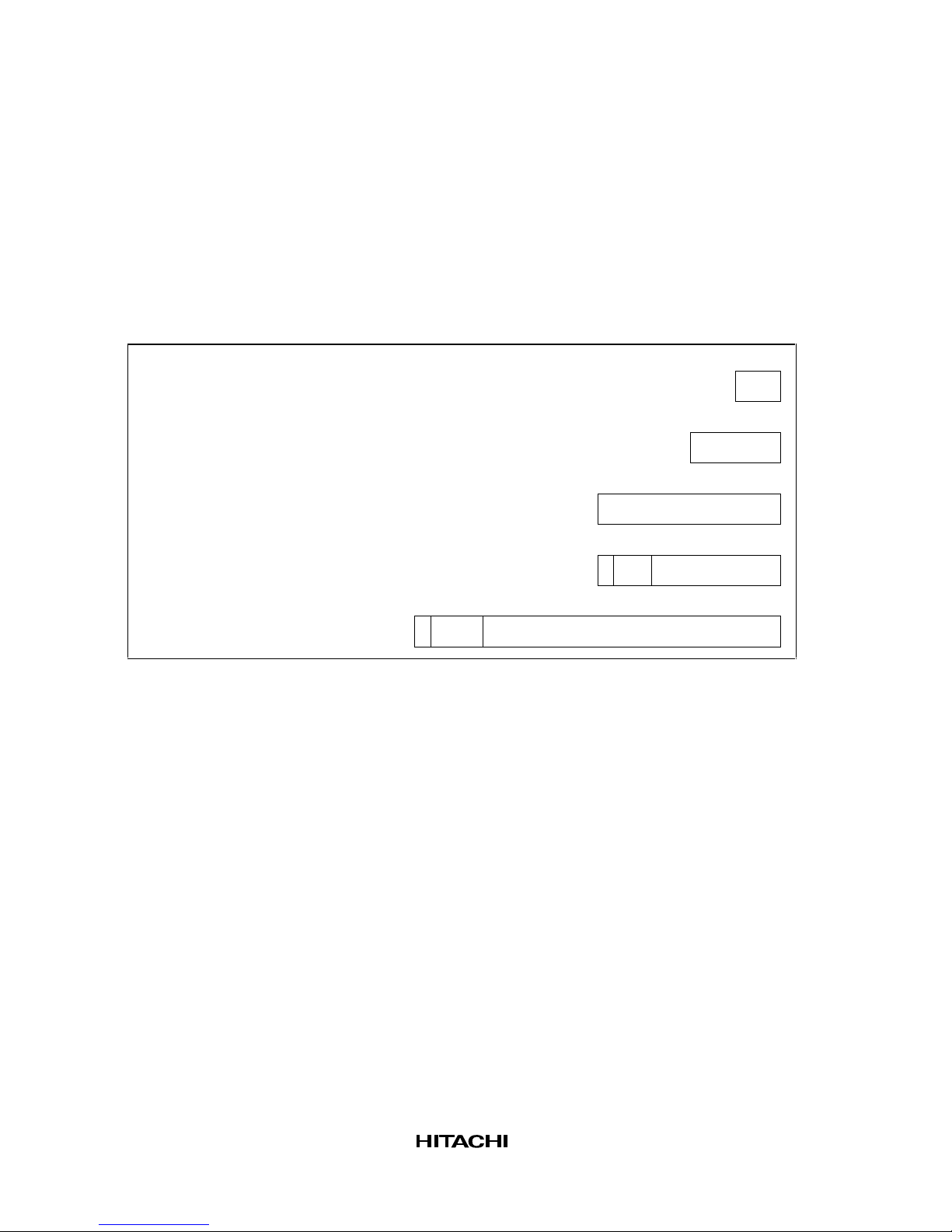
1.2 Block Diagram
Figure 1.1 shows an internal block diagram of the SH7750.
CPG
INTC
SCI
(SCIF)
RTC
TMU
External
bus interface
BSC
DMAC
Address
29-bit address
64-bit data
64-bit data
32-bit data
32-bit data
Upper 32-bit data
32-bit address (instructions)
32-bit data (instructions)
32-bit address (data)
Peripheral address bus
26-bit
address
64-bit
data
16-bit peripheral data bus
UBC
Lower 32-bit data
Lower 32-bit data
32-bit data (load)
32-bit data (store)
CPU
I cache
(8 kB)
O cache
(16 kB)
ITLB UTLBCCN
FPU
64-bit data (store)
CCN: Cache and TLB controller
BSC: Bus state controller
CPG: Clock pulse generator
DMAC: Direct memory access controller
FPU: Floating-point unit
INTC: Interrupt controller
ITLB: Instruction TLB (translation lookaside buffer)
UTLB: Unified TLB (translation lookaside buffer)
RTC: Realtime clock
SCI: Serial communication interface
SCIF: Serial communication interface with FIFO
TMU: Timer unit
UBC: User break controller
Figure 1.1 Block Diagram of SH7750 Function s
Rev. 2.0, 03/98, page 9 of 396
Section 2 Programming Model
2.1 Data Formats
The data formats handled by the SH7750 are shown in figure 2.1.
Byte (8 bits)
Word (16 bits)
Longword (32 bits)
Single-precision floating-point (32 bits)
Double-precision floating-point (64 bits)
07
015
031
031 30 22
fractionexps
063 62 51
exps fraction
Figure 2.1 Data Formats

Rev. 2.0, 03/98, page 10 of 396
2.2 Register Configuration
2.2.1 Privileged Mode and Banks
Processor Modes: The SH7750 has two processor modes, user mode and privileged mode. The
SH7750 normally operates in user mode, and switches to privileged mode when an exception
occurs or an interrupt is accepted. There are four kinds of registers—general registers, system
registers, control registers, and floating-point registers—and the registers that can be accessed
differ in the two processor modes.
General Registers: There are 16 general registers, designated R0 to R15. General registers R0 to
R7 are banked registers which are switched by a processor mode change.
In privileged mode, the regist er bank bit (RB) in the status register (SR) defines which banked
register set is accessed as general registers, and which set is accessed only through the load control
register (LDC) and store control register (STC) instructions.
When the RB bit is 1 (that is, whe n bank 1 is selected), the 16 regi sters comprising bank 1 general
registers R0_BANK1 to R7_BANK1 and non-banked general registers R8 to R15 can be accessed
as general registe rs R0 to R15. In this case, the eight registers comprising bank 0 general registers
R0_BANK0 to R7_BANK0 are accessed by the LDC/STC instructions. When the RB bit is 0 (that
is, when bank 0 is selected), the 16 registers com prising bank 0 general registers R0_BANK0 to
R7_BANK0 and non-banked general registers R8 to R15 can be accessed as general registers R0
to R15. In this case, the eight registers comprising bank 1 general registers R0_BANK1 to
R7_BANK1 are accessed by the LDC/STC instructions.
In user mode, the 16 registers comprising bank 0 general reg i sters R0_BANK0 to R7_BANK0 and
non-banked general registers R8 to R15 can be accessed as general registers R0 to R15. The eight
registers comprising bank 1 general registers R0_BANK1 to R7_BANK1 cannot be accessed.
Control Registers: Control registers comprise the global base register (GBR) and status register
(SR), which can be accessed in both processor modes, and the saved status register (SSR), saved
program counter (SPC), vector base register (VBR), saved general register 15 (SGR), and debug
base register (DBR), which can only be accessed in privileged mode. Some bits of the status
register (such as the RB bit) can only be accessed in privileged mode.
System Registers: System registers comprise the multiply-and-accumulate registers
(MACH/MACL), the procedure register (PR), the program counter (PC), the fl oating-point
status/control register (FPSCR), and the floating-point communication register (FPUL). Access to
these registers does not depend on the processor mo de.

Rev. 2.0, 03/98, page 11 of 396
Floating-Point Registers: There are thirty-t wo floating-point registers, FR0–FR15 and XF0–
XF15. FR0–F R 15 and XF0–XF15 can be assigned to eithe r of two banks (FPR0_BAN K0–
FPR15_BANK0 or FPR0_BANK1–FPR15_BANK1).
FR0–FR15 can be used as the eight registers DR 0/2/4/6/8/1 0/12/14 (double -precision floatingpoint registers, or pair registers) or the four registers FV0/4/8/12 (register vectors), while XF0–
XF15 can be used as the eight registers XD0/2/4/6/8/10/12/ 14 (register pairs) or register matrix
XMTRX.
Register values after a reset are shown in table 2.1.
Table 2.1 Initial Register Values
Type Registers Initial Value*
General registers R0_BANK0–R7_BANK0,
R0_BANK1–R7_BANK1,
R8–R15
Undefined
SR MD bit = 1, RB bit = 1, BL bit = 1, FD bit = 0,
I3–I0 = 1111 (H'F), reserved bits = 0, others
undefined
GBR, SSR, SPC, SGR,
DBR
Undefined
Control registers
VBR H'00000000
MACH, MACL, PR, FPUL Undefined
PC H'A0000000
System registers
FPSCR H'00040001
Floating-point
registers
FR0–FR15, XF0–XF15 Undefined
Note: * Initialized by a power-on reset and manual reset.
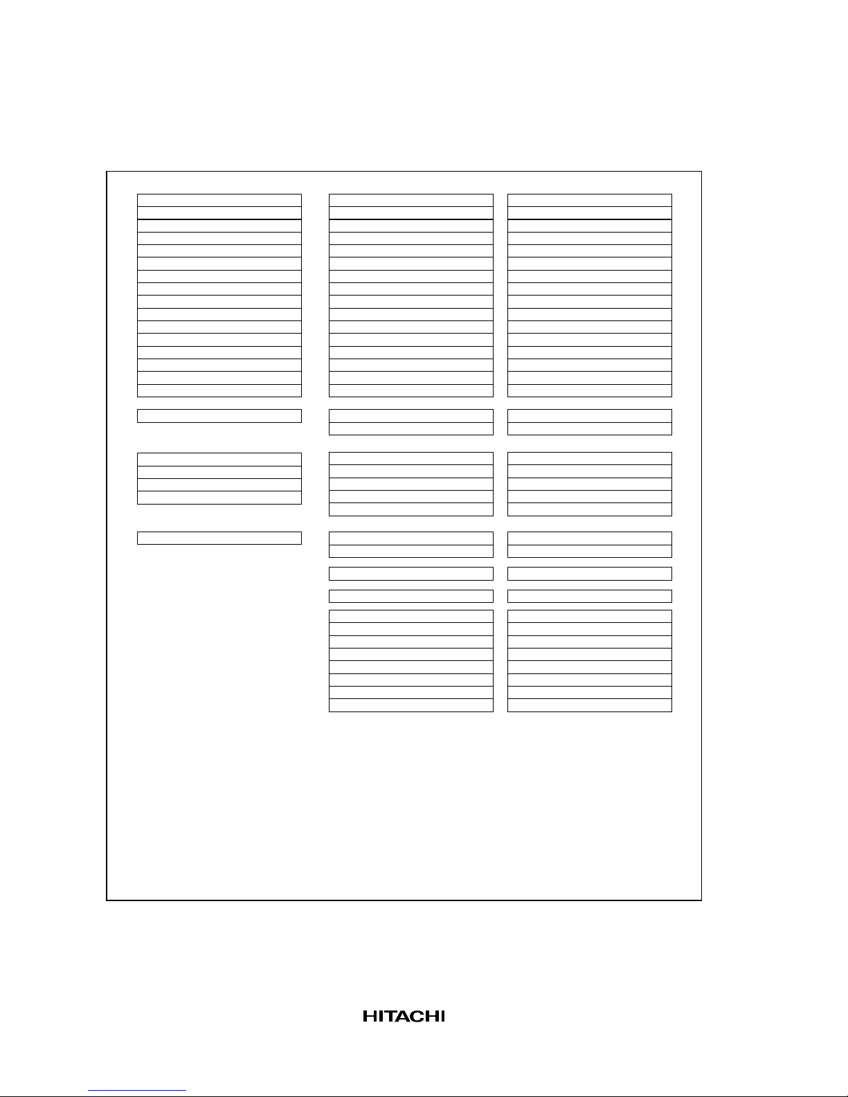
The register configuration in each processor is shown in figure 2.2.
Switching betwee n user mode and privileged mode is controlled by the processor mode bit (MD)
in the status register.
Rev. 2.0, 03/98, page 12 of 396
31 0
R0_BANK0*
1,*2
R1_BANK0*
2
R2_BANK0*
2
R3_BANK0*
2
R4_BANK0*
2
R5_BANK0*
2
R6_BANK0*
2
R7_BANK0*
2
R8
R9
R10
R11
R12
R13
R14
R15
SR
GBR
MACH
MACL
PR
PC
(a) Register configuration
in user mode
31 0
R0_BANK1*
1,*3
R1_BANK1*
3
R2_BANK1*
3
R3_BANK1*
3
R4_BANK1*
3
R5_BANK1*
3
R6_BANK1*
3
R7_BANK1*
3
R8
R9
R10
R11
R12
R13
R14
R15
R0_BANK0*1,*
4
R1_BANK0*
4
R2_BANK0*
4
R3_BANK0*
4
R4_BANK0*
4
R5_BANK0*
4
R6_BANK0*
4
R7_BANK0*
4
(b) Register configuration in
privileged mode (RB = 1)
GBR
MACH
MACL
VBR
PR
SR
SSR
PC
SPC
31 0
R0_BANK1*
1,*3
R1_BANK1*
3
R2_BANK1*
3
R3_BANK1*
3
R4_BANK1*
3
R5_BANK1*
3
R6_BANK1*
3
R7_BANK1*
3
R8
R9
R10
R11
R12
R13
R14
R15
R0_BANK0*1,*
4
R1_BANK0*
4
R2_BANK0*
4
R3_BANK0*
4
R4_BANK0*
4
R5_BANK0*
4
R6_BANK0*
4
R7_BANK0*
4
(c) Register configuration in
privileged mode (RB = 0)
GBR
MACH
MACL
VBR
PR
SR
SSR
PC
SPC
SGR
DBR
SGR
DBR
Notes: 1. The R0 register is used as the index register in indexed register-indirect addressing mode and
indexed GBR indirect addressing mode.
2. Banked registers
3. Banked registers
Accessed as general registers when the RB bit is set to 1 in the SR register. Accessed only by
LDC/STC instructions when the RB bit is cleared to 0.
4. Banked registers
Accessed as general registers when the RB bit is cleared to 0 in the SR register. Accessed only by
LDC/STC instructions when the RB bit is set to 1.
Figure 2.2 CPU Register Configuration in Each Processor Mode

Rev. 2.0, 03/98, page 13 of 396
2.2.2 General Registers
Figure 2.3 shows the relationsh ip between the processor modes and general registers. The SH7750
has twenty-fo ur 32-bit general registers (R0_BANK0–R7_BANK0, R0_BANK1–R7_BANK1,
and R8–R15). However, only 16 of these can be accessed as general registers R0–R15 in one
processor mode. The SH7750 has two processor mo des, user mode and privileged mode, in which
R0–R7 are assigned as shown below.
• R0_BANK0–R7_BANK0
In user mode (SR.MD = 0), R0–R7 are always assigned to R0_BANK0–R7_BANK0.
In privileged mode (SR.MD = 1), R0–R7 are assigned to R0_BANK0– R7_BANK0 only when
SR.RB = 0.
• R0_BANK1–R7_BANK1
In user mode, R0_BANK1–R7_BANK1 cannot be accessed.
In privileged mode, R0–R7 are assigned to R0_BANK1–R7_BANK1 only when SR.RB = 1.

Rev. 2.0, 03/98, page 14 of 396
SR.MD = 0 or
(SR.MD = 1, SR.RB = 0)
R0_BANK0
R1_BANK0
R2_BANK0
R3_BANK0
R4_BANK0
R5_BANK0
R6_BANK0
R7_BANK0
R0_BANK0
R1_BANK0
R2_BANK0
R3_BANK0
R4_BANK0
R5_BANK0
R6_BANK0
R7_BANK0
R0_BANK1
R1_BANK1
R2_BANK1
R3_BANK1
R4_BANK1
R5_BANK1
R6_BANK1
R7_BANK1
R0_BANK1
R1_BANK1
R2_BANK1
R3_BANK1
R4_BANK1
R5_BANK1
R6_BANK1
R7_BANK1
R0
R1
R2
R3
R4
R5
R6
R7
R0
R1
R2
R3
R4
R5
R6
R7
R8
R9
R10
R11
R12
R13
R14
R15
R8
R9
R10
R11
R12
R13
R14
R15
R8
R9
R10
R11
R12
R13
R14
R15
(SR.MD = 1, SR.RB = 1)
Figure 2.3 General Registers
Programmin g Note: As the user’s R0–R7 are assigned to R0_BANK0–R7_BANK0, and after an
exception or interrupt R0–R7 are assigned to R0_BANK1–R7_BANK1, it is not necessary for the
interrupt handle r to save and restore the user ’s R0–R7 (R0_BANK0–R7_BANK0).
After a reset, the values of R0_BANK0–R7_BANK0, R0_BANK1–R7_BANK1, and R8–R15 ar e
undefined.

Rev. 2.0, 03/98, page 15 of 396
2.2.3 Floating-Point Registers
Figure 2.4 shows the floating-point registers. There are thirty-two 32-bit floating-point registers,
divided into tw o banks (FPR0_BANK0–FPR15_BANK0 and FPR0_BANK1– FPR15_BANK 1).
These 32 regi sters are refe renced as FR0–FR15, DR0/2/4/6/8/10/12/14, FV0/4/8/12, XF 0–XF15,
XD0/2/4/6/8/10/12/14, or XMTRX. The correspondence betwe en FPRn_BANKi and the re ference
name is determined by the FR bit in FPSCR (see figure 2.4).
• Floating-point registers, FPRn_BA N Ki (32 register s)
FPR0_BANK0, FPR1_BANK0, FPR2_BANK0, FPR3_BANK 0, FP R4_BANK0,
FPR5_BANK0, FPR6_BANK0, FPR7_BANK0, FPR8_BANK 0, FP R9_BANK0,
FPR10_BANK0, FPR11_BANK0, FPR12_BANK0, FPR13_BANK0, FPR 1 4_BANK0,
FPR15_BANK0
FPR0_BANK1, FPR1_BANK1, FPR2_BANK1, FPR3_BANK 1, FP R4_BANK1,
FPR5_BANK1, FPR6_BANK1, FPR7_BANK1, FPR8_BANK 1, FP R9_BANK1,
FPR10_BANK1, FPR11_BANK1, FPR12_BANK1, FPR13_BANK1, FPR 1 4_BANK1,
FPR15_BANK1
• Single-precision floating-point registers, FRi ( 16 registers)
When FPSCR.FR = 0, FR0–FR15 are assigned to FPR0_BANK0–FPR15_BANK0.
When FPSCR.FR = 1, FR0–FR15 are assigned to FPR0_BANK1–FPR15_BANK1.
• Double-preci sion floating- point registers or single-precision floati ng-point register pairs, DRi
(8 registers): A DR register comprises two FR registers.
DR0 = {FR0, FR1}, DR2 = {FR2, FR3}, DR4 = {FR4, FR5}, DR6 = {FR6, FR7},
DR8 = {FR8, FR9}, DR10 = {FR10, FR11}, DR12 = {FR12, FR13}, DR14 = {FR14, FR15}
• Single-precision floating-point vector registers, FVi (4 registers): An FV register c om prises
four FR regis t ers
FV0 = {FR0, FR1, FR2, FR3}, FV4 = {FR4, F R5, FR6, FR7},
FV8 = {FR8, FR9, FR10, FR11}, FV12 = {FR12, FR13, FR14, FR15}
• Single-precision floating- point extended r egisters, XFi ( 16 registers)
When FPSCR.FR = 0, XF0–XF1 5 are assigned to FPR0_BANK1–FPR15_BANK1.
When FPSCR.FR = 1, XF0–XF1 5 are assigned to FPR0_BANK0–FPR15_BANK0.
• Single-precision floating- point extended r egister pairs, X Di (8 registers): An XD register
comprises two XF register s
XD0 = {XF0, XF1}, XD2 = {XF2, XF3}, XD4 = {XF4, XF5}, XD6 = {XF6, XF7},
XD8 = {XF8, XF9}, XD10 = {XF10, XF11}, XD12 = {XF12, XF13}, XD14 = {XF14, XF15}

Rev. 2.0, 03/98, page 16 of 396
• Single-precision floating- point extended r egister matrix, X MTRX: XMTRX comprises all 16
XF registers
XMTRX = XF0 XF4 XF8 XF12
XF1 XF5 XF9 XF13
XF2 XF6 XF10 XF14
XF3 XF7 XF11 XF15
FPR0_BANK0
FPR1_BANK0
FPR2_BANK0
FPR3_BANK0
FPR4_BANK0
FPR5_BANK0
FPR6_BANK0
FPR7_BANK0
FPR8_BANK0
FPR9_BANK0
FPR10_BANK0
FPR11_BANK0
FPR12_BANK0
FPR13_BANK0
FPR14_BANK0
FPR15_BANK0
XF0
XF1
XF2
XF3
XF4
XF5
XF6
XF7
XF8
XF9
XF10
XF11
XF12
XF13
XF14
XF15
FR0
FR1
FR2
FR3
FR4
FR5
FR6
FR7
FR8
FR9
FR10
FR11
FR12
FR13
FR14
FR15
DR0
DR2
DR4
DR6
DR8
DR10
DR12
DR14
FV0
FV4
FV8
FV12
XD0 XMTRX
XD2
XD4
XD6
XD8
XD10
XD12
XD14
FPR0_BANK1
FPR1_BANK1
FPR2_BANK1
FPR3_BANK1
FPR4_BANK1
FPR5_BANK1
FPR6_BANK1
FPR7_BANK1
FPR8_BANK1
FPR9_BANK1
FPR10_BANK1
FPR11_BANK1
FPR12_BANK1
FPR13_BANK1
FPR14_BANK1
FPR15_BANK1
XF0
XF1
XF2
XF3
XF4
XF5
XF6
XF7
XF8
XF9
XF10
XF11
XF12
XF13
XF14
XF15
FR0
FR1
FR2
FR3
FR4
FR5
FR6
FR7
FR8
FR9
FR10
FR11
FR12
FR13
FR14
FR15
DR0
DR2
DR4
DR6
DR8
DR10
DR12
DR14
FV0
FV4
FV8
FV12
XD0XMTRX
XD2
XD4
XD6
XD8
XD10
XD12
XD14
FPSCR.FR = 0
FPSCR.FR = 1
Figure 2.4 Floating-Point Registers
 Loading...