

Hitachi SH7709S Hardware Manual

To all our customers
Regarding the change of names mentioned in the document, such as
Hitachi Electric and Hitachi XX, to Renesas Technology Corp.
The semiconductor operations of Mitsubishi Electric and Hitachi were
transferred to Renesas Technology Corporation on April 1st 2003.
These operations include microcomputer, logic, analog and discrete devices,
and memory chips other than DRAMs (flash memory, SRAMs etc.)
Accordingly, although Hitachi, Hitachi, Ltd., Hitachi Semiconductors,
and other Hitachi brand names are mentioned in the document, these names
have in fact all been changed to Renesas Technology Corp.
Thank you for your understanding. Except for our corporate trademark,
logo and corporate statement, no changes whatsoever have been made to the
contents of the document, and these changes do not constitute any alteration
to the contents of the document itself.
Renesas Technology Home Page: www.renesas.com
Renesas Technology Corp.
Customer Support Dept.
April 1, 2003
Renesas Technology Corp.
查询HD6417709供应商 捷多邦,专业PCB打样工厂,24小时加急出货

Hitachi SuperH™ RISC engine
SH7709S
Hardware Manual
ADE-602-250
Rev. 1.0
09/21/01
Hitachi, Ltd.

Cautions
1. Hitachi neither warrants nor grants licenses of any rights of Hitachi’s or any third party’s
patent, copyright, trademark, or other intellectual property rights for information contained in
this document. Hitachi bears no responsibility for problems that may arise with third party’s
rights, including intellectual property rights, in connection with use of the information
contained in this document.
2. Products and product specifications may be subject to change without notice. Confirm that you
have received the latest product standards or specifications before final design, purchase or
use.
3. Hitachi makes every attempt to ensure that its products are of high quality and reliability.
However, contact Hitachi’s sales office before using the product in an application that
demands especially high quality and reliability or where its failure or malfunction may directly
threaten human life or cause risk of bodily injury, such as aerospace, aeronautics, nuclear
power, combustion control, transportation, traffic, safety equipment or medical equipment for
life support.
4. Design your application so that the product is used within the ranges guaranteed by Hitachi
particularly for maximum rating, operating supply voltage range, heat radiation characteristics,
installation conditions and other characteristics. Hitachi bears no responsibility for failure or
damage when used beyond the guaranteed ranges. Even within the guaranteed ranges,
consider normally foreseeable failure rates or failure modes in semiconductor devices and
employ systemic measures such as fail-safes, so that the equipment incorporating Hitachi
product does not cause bodily injury, fire or other consequential damage due to operation of
the Hitachi product.
5. This product is not designed to be radiation resistant.
6. No one is permitted to reproduce or duplicate, in any form, the whole or part of this document
without written approval from Hitachi.
7. Contact Hitachi’s sales office for any questions regarding this document or Hitachi
semiconductor products.

Preface
This LSI is a microprocessor with the 32-bit SH-3 CPU as its core and peripheral functions
necessary for configuring a user system.
This LSI is built in with a variety of peripheral functions such as cache memory, memory
management unit (MMU), interrupt controller, timer, three serial communication interfaces, realtime clock (RTC), use break controller (UBC), bus state controller (BSC) and I/O ports.
This LSI can be used as a microcomputer for devices that require both high speed and low power
consumption.
Target Readers: This manual is designed for use by people who design application systems using
the SH7709S.
To use this manual, basic knowledge of electric circuits, logic circuits and microcomputers is
required.
Purpose: This manual provides the information of the hardware functions and electrical
characteristics of the SH7709S.
The SH3, SH-3E, SH3-DSP Programming Manual contains detailed information of executable
instructions. Please read the Programming Manual together with this manual.
How to Use the Book:
• To understand general functions
Read the manuala from the beginning.
The manual explains the CPU, system control functions, peripheral functions and electrical
characteristics in that order.
• To understanding CPU functions
Refer to the separate SH3, SH-3E, SH3-DSP Programming Manual.
Explanatory Note: Bit sequence: upper bit at left, and lower bit at right
List of Related Documents: The latest documents are available on our Web site. Please make
sure that you have the latest version.
(http://www.hitachi.co.jp/Sicd/English/Products/micome.htm
• User manuals for SH7709S
Name of Document Document No.
SH7709S Series Hardware Manual This manual
SH3, SH-3E, SH3-DSP Programming Manual ADE-602-156

• User manuals for development tools
Name of Document Document No.
C/C++ Compiler, Assembler, Optimizing Linkage Editor User’s Manual ADE-702-246
Simulator/Debugger User’s Manual ADE-702-186
Hitachi Embedded Workshop User’s Manual ADE-702-201
• Application note
Name of Document Document No.
C/C++ Compiler Guide ADE-xxx-xxx

i
Contents
Section 1 Overview and Pin Functions........................................................................ 1
1.1 SH7709S Features.............................................................................................................. 1
1.2 Block Diagram.................................................................................................................... 6
1.3 Pin Description................................................................................................................... 7
1.3.1 Pin Assignment ..................................................................................................... 7
1.3.2 Pin Function .......................................................................................................... 9
Section 2 CPU...................................................................................................................... 19
2.1 Register Configuration.......................................................................................................19
2.1.1 Privileged Mode and Banks .................................................................................. 19
2.1.2 General Registers .................................................................................................. 22
2.1.3 System Registers ................................................................................................... 23
2.1.4 Control Registers................................................................................................... 23
2.2 Data Formats...................................................................................................................... 25
2.2.1 Data Format in Registers....................................................................................... 25
2.2.2 Data Format in Memory........................................................................................ 25
2.3 Instruction Features............................................................................................................ 26
2.3.1 Execution Environment......................................................................................... 26
2.3.2 Addressing Modes ................................................................................................ 28
2.3.3 Instruction Formats ............................................................................................... 32
2.4 Instruction Set .................................................................................................................... 35
2.4.1 Instruction Set Classified by Function .................................................................. 35
2.4.2 Instruction Code Map............................................................................................ 51
2.5 Processor States and Processor Modes............................................................................... 54
2.5.1 Processor States..................................................................................................... 54
2.5.2 Processor Modes ................................................................................................... 55
Section 3 Memory Management Unit (MMU).......................................................... 57
3.1 Overview............................................................................................................................ 57
3.1.1 Features ................................................................................................................. 57
3.1.2 Role of MMU........................................................................................................ 57
3.1.3 SH7709S MMU .................................................................................................... 60
3.1.4 Register Configuration.......................................................................................... 65
3.2 Register Description........................................................................................................... 65
3.3 TLB Functions.................................................................................................................... 67
3.3.1 Configuration of the TLB...................................................................................... 67
3.3.2 TLB Indexing........................................................................................................ 69
3.3.3 TLB Address Comparison .................................................................................... 70
3.3.4 Page Management Information ............................................................................. 72

ii
3.4 MMU Functions................................................................................................................. 73
3.4.1 MMU Hardware Management .............................................................................. 73
3.4.2 MMU Software Management................................................................................ 73
3.4.3 MMU Instruction (LDTLB).................................................................................. 74
3.4.4 Avoiding Synonym Problems ............................................................................... 76
3.5 MMU Exceptions...............................................................................................................78
3.5.1 TLB Miss Exception ............................................................................................. 78
3.5.2 TLB Protection Violation Exception .................................................................... 79
3.5.3 TLB Invalid Exception.......................................................................................... 80
3.5.4 Initial Page Write Exception ................................................................................. 81
3.5.5 Processing Flow in Event of MMU Exception
(Same Processing Flow for Address Error) .......................................................... 83
3.6 Configuration of Memory-Mapped TLB............................................................................ 84
3.6.1 Data Array............................................................................................................. 85
3.6.2 Usage Examples.................................................................................................... 87
3.7 Usage Note......................................................................................................................... 87
Section 4 Exception Handling........................................................................................ 89
4.1 Overview............................................................................................................................ 89
4.1.1 Features ................................................................................................................. 89
4.1.2 Register Configuration.......................................................................................... 89
4.2 Exception Handling Function............................................................................................. 89
4.2.1 Exception Handling Flow...................................................................................... 89
4.2.2 Exception Vector Addresses ................................................................................. 90
4.2.3 Acceptance of Exceptions ..................................................................................... 92
4.2.4 Exception Codes.................................................................................................... 94
4.2.5 Exception Request Masks ..................................................................................... 95
4.2.6 Returning from Exception Handling..................................................................... 95
4.3 Register Descriptions.......................................................................................................... 96
4.4 Exception Handling Operation........................................................................................... 97
4.4.1 Reset......................................................................................................................97
4.4.2 Interrupts ............................................................................................................... 97
4.4.3 General Exceptions ............................................................................................... 98
4.5 Individual Exception Operations........................................................................................ 98
4.5.1 Resets .................................................................................................................... 98
4.5.2 General Exceptions ............................................................................................... 99
4.5.3 Interrupts ............................................................................................................... 102
4.6 Cautions.............................................................................................................................. 104
Section 5 Cache................................................................................................................... 107
5.1 Overview............................................................................................................................ 107
5.1.1 Features ................................................................................................................. 107
5.1.2 Cache Structure ..................................................................................................... 107

iii
5.1.3 Register Configuration.......................................................................................... 109
5.2 Register Description........................................................................................................... 109
5.2.1 Cache Control Register (CCR).............................................................................. 109
5.2.2 Cache Control Register 2 (CCR2) ........................................................................ 110
5.3 Cache Operation................................................................................................................. 113
5.3.1 Searching the Cache.............................................................................................. 113
5.3.2 Read Access .......................................................................................................... 115
5.3.3 Prefetch Operation ................................................................................................ 115
5.3.4 Write Access ......................................................................................................... 115
5.3.5 Write-Back Buffer................................................................................................. 115
5.3.6 Coherency of Cache and External Memory.......................................................... 116
5.4 Memory-Mapped Cache..................................................................................................... 116
5.4.1 Address Array ....................................................................................................... 116
5.4.2 Data Array............................................................................................................. 117
5.4.3 Examples of Usage................................................................................................ 119
Section 6 Interrupt Controller (INTC).......................................................................... 121
6.1 Overview............................................................................................................................ 121
6.1.1 Features ................................................................................................................. 121
6.1.2 Block Diagram ...................................................................................................... 122
6.1.3 Pin Configuration.................................................................................................. 123
6.1.4 Register Configuration.......................................................................................... 124
6.2 Interrupt Sources................................................................................................................ 125
6.2.1 NMI Interrupt........................................................................................................ 125
6.2.2 IRQ Interrupts ....................................................................................................... 125
6.2.3 IRL Interrupts........................................................................................................ 126
6.2.4 PINT Interrupts ..................................................................................................... 128
6.2.5 On-Chip Peripheral Module Interrupts ................................................................. 128
6.2.6 Interrupt Exception Handling and Priority............................................................ 129
6.3 INTC Registers................................................................................................................... 135
6.3.1 Interrupt Priority Registers A to E (IPRA–IPRE)................................................. 135
6.3.2 Interrupt Control Register 0 (ICR0)...................................................................... 136
6.3.3 Interrupt Control Register 1 (ICR1)...................................................................... 137
6.3.4 Interrupt Control Register 2 (ICR2)...................................................................... 140
6.3.5 PINT Interrupt Enable Register (PINTER)........................................................... 141
6.3.6 Interrupt Request Register 0 (IRR0) ..................................................................... 142
6.3.7 Interrupt Request Register 1 (IRR1) ..................................................................... 144
6.3.8 Interrupt Request Register 2 (IRR2) ..................................................................... 145
6.4 INTC Operation.................................................................................................................. 147
6.4.1 Interrupt Sequence ................................................................................................ 147
6.4.2 Multiple Interrupts ................................................................................................ 149
6.5 Interrupt Response Time......................................................................................................... 149

iv
Section 7 User Break Controller.................................................................................... 153
7.1 Overview............................................................................................................................ 153
7.1.1 Features ................................................................................................................. 153
7.1.2 Block Diagram ...................................................................................................... 154
7.1.3 Register Configuration.......................................................................................... 155
7.2 Register Descriptions.......................................................................................................... 156
7.2.1 Break Address Register A (BARA) ...................................................................... 156
7.2.2 Break Address Mask Register A (BAMRA)......................................................... 157
7.2.3 Break Bus Cycle Register A (BBRA)................................................................... 158
7.2.4 Break Address Register B (BARB) ...................................................................... 160
7.2.5 Break Address Mask Register B (BAMRB)......................................................... 161
7.2.6 Break Data Register B (BDRB) ............................................................................ 162
7.2.7 Break Data Mask Register B (BDMRB)............................................................... 163
7.2.8 Break Bus Cycle Register B (BBRB) ................................................................... 164
7.2.9 Break Control Register (BRCR) ........................................................................... 166
7.2.10 Execution Times Break Register (BETR)............................................................. 170
7.2.11 Branch Source Register (BRSR) ........................................................................... 171
7.2.12 Branch Destination Register (BRDR) ................................................................... 172
7.2.13 Break ASID Register A (BASRA)........................................................................ 173
7.2.14 Break ASID Register B (BASRB) ........................................................................ 173
7.3 Operation Description........................................................................................................ 174
7.3.1 Flow of the User Break Operation ........................................................................ 174
7.3.2 Break on Instruction Fetch Cycle.......................................................................... 175
7.3.3 Break by Data Access Cycle ................................................................................. 175
7.3.4 Sequential Break ................................................................................................... 176
7.3.5 Value of Saved Program Counter.......................................................................... 176
7.3.6 PC Trace................................................................................................................ 177
7.3.7 Usage Examples.................................................................................................... 178
7.3.8 Notes...................................................................................................................... 182
Section 8 Power-Down Modes....................................................................................... 185
8.1 Overview............................................................................................................................ 185
8.1.1 Power-Down Modes.............................................................................................. 185
8.1.2 Pin Configuration.................................................................................................. 187
8.1.3 Register Configuration.......................................................................................... 187
8.2 Register Descriptions.......................................................................................................... 187
8.2.1 Standby Control Register (STBCR)...................................................................... 187
8.2.2 Standby Control Register 2 (STBCR2)................................................................. 189
8.3 Sleep Mode......................................................................................................................... 191
8.3.1 Transition to Sleep Mode...................................................................................... 191
8.3.2 Canceling Sleep Mode .......................................................................................... 191
8.4 Standby Mode .................................................................................................................... 192
8.4.1 Transition to Standby Mode.................................................................................. 192

v
8.4.2 Canceling Standby Mode ...................................................................................... 193
8.4.3 Clock Pause Function............................................................................................ 194
8.5 Module Standby Function.................................................................................................. 195
8.5.1 Transition to Module Standby Function................................................................ 195
8.5.2 Clearing Module Standby Function ...................................................................... 195
8.6 Timing of STATUS Pin Changes....................................................................................... 196
8.6.1 Timing for Resets.................................................................................................. 196
8.6.2 Timing for Canceling Standby.............................................................................. 198
8.6.3 Timing for Canceling Sleep Mode........................................................................ 200
8.7 Hardware Standby Mode.................................................................................................... 203
8.7.1 Transition to Hardware Standby Mode ................................................................. 203
8.7.2 Canceling Hardware Standby Mode...................................................................... 204
8.7.3 Hardware Standby Mode Timing.......................................................................... 204
Section 9 On-Chip Oscillation Circuits ....................................................................... 207
9.1 Overview............................................................................................................................ 207
9.1.1 Features ................................................................................................................. 207
9.2 Overview of CPG............................................................................................................... 208
9.2.1 CPG Block Diagram.............................................................................................. 208
9.2.2 CPG Pin Configuration ......................................................................................... 210
9.2.3 CPG Register Configuration ................................................................................. 210
9.3 Clock Operating Modes...................................................................................................... 211
9.4 Register Descriptions.......................................................................................................... 215
9.4.1 Frequency Control Register (FRQCR).................................................................. 215
9.5 Changing the Frequency..................................................................................................... 217
9.5.1 Changing the Multiplication Rate ......................................................................... 217
9.5.2 Changing the Division Ratio................................................................................. 217
9.6 Overview of WDT.............................................................................................................. 218
9.6.1 Block Diagram of WDT........................................................................................ 218
9.6.2 Register Configuration.......................................................................................... 218
9.7 WDTRegisters.................................................................................................................... 219
9.7.1 Watchdog Timer Counter (WTCNT).................................................................... 219
9.7.2 Watchdog Timer Control/Status Register (WTCSR)............................................ 219
9.7.3 Notes on Register Access...................................................................................... 221
9.8 Using the WDT.................................................................................................................. 222
9.8.1 Canceling Standby ................................................................................................ 222
9.8.2 Changing the Frequency........................................................................................ 222
9.8.3 Using Watchdog Timer Mode............................................................................... 223
9.8.4 Using Interval Timer Mode................................................................................... 223
9.9 Notes on Board Design ...................................................................................................... 224
Section 10 Bus State Controller (BSC).......................................................................... 227
10.1 Overview............................................................................................................................ 227

vi
10.1.1 Features ................................................................................................................. 227
10.1.2 Block Diagram ...................................................................................................... 229
10.1.3 Pin Configuration.................................................................................................. 230
10.1.4 Register Configuration.......................................................................................... 232
10.1.5 Area Overview ...................................................................................................... 233
10.1.6 PCMCIA Support.................................................................................................. 236
10.2 BSC Registers .................................................................................................................... 239
10.2.1 Bus Control Register 1 (BCR1) ............................................................................ 239
10.2.2 Bus Control Register 2 (BCR2) ............................................................................ 243
10.2.3 Wait State Control Register 1 (WCR1)................................................................. 244
10.2.4 Wait State Control Register 2 (WCR2)................................................................. 245
10.2.5 Individual Memory Control Register (MCR)........................................................ 249
10.2.6 PCMCIA Control Register (PCR)......................................................................... 252
10.2.7 Synchronous DRAM Mode Register (SDMR) ..................................................... 256
10.2.8 Refresh Timer Control/Status Register (RTCSR)................................................. 257
10.2.9 Refresh Timer Counter (RTCNT) ......................................................................... 259
10.2.10 Refresh Time Constant Register (RTCOR) .......................................................... 260
10.2.11 Refresh Count Register (RFCR) ........................................................................... 260
10.2.12 Cautions on Accessing Refresh Control Related Registers .................................. 261
10.2.13 MCS0 Control Register (MCSCR0) ..................................................................... 262
10.2.14 MCS1 Control Register (MCSCR1) ..................................................................... 263
10.2.15 MCS2 Control Register (MCSCR2) ..................................................................... 263
10.2.16 MCS3 Control Register (MCSCR3) ..................................................................... 263
10.2.17 MCS4 Control Register (MCSCR4) ..................................................................... 263
10.2.18 MCS5 Control Register (MCSCR5) ..................................................................... 263
10.2.19 MCS6 Control Register (MCSCR6) ..................................................................... 263
10.2.20 MCS7 Control Register (MCSCR7) ..................................................................... 263
10.3 BSC Operation.................................................................................................................... 264
10.3.1 Endian/Access Size and Data Alignment.............................................................. 264
10.3.2 Description of Areas.............................................................................................. 269
10.3.3 Basic Interface....................................................................................................... 272
10.3.4 Synchronous DRAM Interface.............................................................................. 280
10.3.5 Burst ROM Interface............................................................................................. 309
10.3.6 PCMCIA Interface ................................................................................................ 312
10.3.7 Waits between Access Cycles ............................................................................... 324
10.3.8 Bus Arbitration...................................................................................................... 325
10.3.9 Bus Pull-Up ........................................................................................................... 326
10.3.10 MCS[0] to MCS[7] Pin Control............................................................................ 328
Section 11 Direct Memory Access Controller (DMAC).......................................... 331
11.1 Overview............................................................................................................................ 331
11.1.1 Features ................................................................................................................. 331
11.1.2 Block Diagram ...................................................................................................... 333

vii
11.1.3 Pin Configuration.................................................................................................. 334
11.1.4 Register Configuration.......................................................................................... 335
11.2 Register Descriptions.......................................................................................................... 337
11.2.1 DMA Source Address Registers 0–3 (SAR0–SAR3) ........................................... 337
11.2.2 DMA Destination Address Registers 0–3 (DAR0–DAR3) .................................. 338
11.2.3 DMA Transfer Count Registers 0–3 (DMATCR0–DMATCR3) ......................... 339
11.2.4 DMA Channel Control Registers 0–3 (CHCR0–CHCR3).................................... 340
11.2.5 DMA Operation Register (DMAOR).................................................................... 347
11.3 Operation............................................................................................................................ 349
11.3.1 DMA Transfer Flow.............................................................................................. 349
11.3.2 DMA Transfer Requests........................................................................................ 351
11.3.3 Channel Priority .................................................................................................... 353
11.3.4 DMA Transfer Types ............................................................................................ 356
11.3.5 Number of Bus Cycle States and DREQ Pin Sampling Timing ........................... 367
11.3.6 Source Address Reload Function.......................................................................... 376
11.3.7 DMA Transfer Ending Conditions........................................................................ 378
11.4 Compare Match Timer (CMT)........................................................................................... 380
11.4.1 Overview ............................................................................................................... 380
11.4.2 Register Descriptions ............................................................................................ 381
11.4.3 Operation............................................................................................................... 384
11.4.4 Compare Match ..................................................................................................... 385
11.5 Examples of Use................................................................................................................. 387
11.5.1 Example of DMA Transfer between On-Chip IrDA and External Memory ........ 387
11.5.2 Example of DMA Transfer between A/D Converter and External Memory........ 388
11.5.3 Example of DMA Transfer between External Memory and SCIF Transmitter
(Indirect Address On)............................................................................................ 389
11.6 Usage Notes........................................................................................................................ 391
Section 12 Timer (TMU).................................................................................................... 393
12.1 Overview............................................................................................................................ 393
12.1.1 Features ................................................................................................................. 393
12.1.2 Block Diagram ...................................................................................................... 394
12.1.3 Pin Configuration.................................................................................................. 395
12.1.4 Register Configuration.......................................................................................... 395
12.2 TMU Registers ................................................................................................................... 396
12.2.1 Timer Output Control Register (TOCR) ............................................................... 396
12.2.2 Timer Start Register (TSTR)................................................................................. 396
12.2.3 Timer Control Registers (TCR) ............................................................................ 397
12.2.4 Timer Constant Registers (TCOR)........................................................................ 401
12.2.5 Timer Counters (TCNT)........................................................................................ 401
12.2.6 Input Capture Register (TCPR2)........................................................................... 403
12.3 TMU Operation.................................................................................................................. 404
12.3.1 General Operation ................................................................................................. 404

viii
12.3.2 Input Capture Function.......................................................................................... 407
12.4 Interrupts ............................................................................................................................ 408
12.4.1 Status Flag Setting Timing.................................................................................... 408
12.4.2 Status Flag Clearing Timing ................................................................................. 409
12.4.3 Interrupt Sources and Priorities............................................................................. 409
12.5 Usage Notes........................................................................................................................ 410
12.5.1 Writing to Registers .............................................................................................. 410
12.5.2 Reading Registers.................................................................................................. 410
Section 13 Realtime Clock (RTC)................................................................................... 411
13.1 Overview............................................................................................................................ 411
13.1.1 Features ................................................................................................................. 411
13.1.2 Block Diagram ...................................................................................................... 412
13.1.3 Pin Configuration.................................................................................................. 413
13.1.4 RTC Register Configuration ................................................................................. 414
13.2 RTC Registers.................................................................................................................... 415
13.2.1 64-Hz Counter (R64CNT) .................................................................................... 415
13.2.2 Second Counter (RSECCNT)................................................................................ 415
13.2.3 Minute Counter (RMINCNT) ............................................................................... 416
13.2.4 Hour Counter (RHRCNT)..................................................................................... 416
13.2.5 Day of Week Counter (RWKCNT)....................................................................... 417
13.2.6 Date Counter (RDAYCNT) .................................................................................. 418
13.2.7 Month Counter (RMONCNT) .............................................................................. 418
13.2.8 Year Counter (RYRCNT) ..................................................................................... 419
13.2.9 Second Alarm Register (RSECAR) ...................................................................... 419
13.2.10 Minute Alarm Register (RMINAR)...................................................................... 420
13.2.11 Hour Alarm Register (RHRAR)............................................................................ 420
13.2.12 Day of Week Alarm Register (RWKAR) ............................................................. 421
13.2.13 Date Alarm Register (RDAYAR) ......................................................................... 422
13.2.14 Month Alarm Register (RMONAR) ..................................................................... 422
13.2.15 RTC Control Register 1 (RCR1)........................................................................... 423
13.2.16 RTC Control Register 2 (RCR2)........................................................................... 424
13.3 RTC Operation ................................................................................................................... 426
13.3.1 Initial Settings of Registers after Power-On ......................................................... 426
13.3.2 Setting the Time .................................................................................................... 426
13.3.3 Reading the Time .................................................................................................. 427
13.3.4 Alarm Function ..................................................................................................... 428
13.3.5 Crystal Oscillator Circuit ...................................................................................... 429
13.4 Usage Notes........................................................................................................................ 430
13.4.1 Register Writing during RTC Count ..................................................................... 430
13.4.2 Use of Realtime Clock (RTC) Periodic Interrupts................................................ 430
Section 14 Serial Communication Interface (SCI)..................................................... 431

ix
14.1 Overview............................................................................................................................ 431
14.1.1 Features ................................................................................................................. 431
14.1.2 Block Diagram ...................................................................................................... 432
14.1.3 Pin Configuration.................................................................................................. 435
14.1.4 Register Configuration.......................................................................................... 436
14.2 Register Descriptions.......................................................................................................... 436
14.2.1 Receive Shift Register (SCRSR)........................................................................... 436
14.2.2 Receive Data Register (SCRDR) .......................................................................... 437
14.2.3 Transmit Shift Register (SCTSR) ......................................................................... 437
14.2.4 Transmit Data Register (SCTDR) ......................................................................... 438
14.2.5 Serial Mode Register (SCSMR)............................................................................ 438
14.2.6 Serial Control Register (SCSCR).......................................................................... 441
14.2.7 Serial Status Register (SCSSR)............................................................................. 445
14.2.8 SC Port Control Register (SCPCR)/SC Port Data Register (SCPDR).................. 449
14.2.9 Bit Rate Register (SCBRR)................................................................................... 451
14.3 Operation............................................................................................................................ 458
14.3.1 Overview ............................................................................................................... 458
14.3.2 Operation in Asynchronous Mode ........................................................................ 460
14.3.3 Multiprocessor Communication............................................................................ 470
14.3.4 Synchronous Operation ......................................................................................... 479
14.4 SCI Interrupts ..................................................................................................................... 489
14.5 Usage Notes........................................................................................................................ 490
Section 15 Smart Card Interface...................................................................................... 493
15.1 Overview............................................................................................................................ 493
15.1.1 Features ................................................................................................................. 493
15.1.2 Block Diagram ...................................................................................................... 494
15.1.3 Pin Configuration.................................................................................................. 495
15.1.4 Smart Card Interface Registers.............................................................................. 495
15.2 Register Descriptions.......................................................................................................... 496
15.2.1 Smart Card Mode Register (SCSCMR) ................................................................ 496
15.2.2 Serial Status Register (SCSSR)............................................................................. 497
15.3 Operation............................................................................................................................ 498
15.3.1 Overview ............................................................................................................... 498
15.3.2 Pin Connections .................................................................................................... 499
15.3.3 Data Format........................................................................................................... 500
15.3.4 Register Settings.................................................................................................... 501
15.3.5 Clock ..................................................................................................................... 502
15.3.6 Data Transmission and Reception......................................................................... 505
15.4 Usage Notes........................................................................................................................ 511
15.4.1 Receive Data Timing and Receive Margin in Asynchronous Mode..................... 511
15.4.2 Retransmission (Receive and Transmit Modes).................................................... 513

x
Section 16 Serial Communication Interface with FIFO (SCIF).............................. 515
16.1 Overview............................................................................................................................ 515
16.1.1 Features ................................................................................................................. 515
16.1.2 Block Diagram ...................................................................................................... 516
16.1.3 Pin Configuration.................................................................................................. 519
16.1.4 Register Configuration.......................................................................................... 520
16.2 Register Descriptions.......................................................................................................... 521
16.2.1 Receive Shift Register (SCRSR)........................................................................... 521
16.2.2 Receive FIFO Data Register (SCFRDR) .............................................................. 521
16.2.3 Transmit Shift Register (SCTSR) ......................................................................... 521
16.2.4 Transmit FIFO Data Register (SCFTDR) ............................................................. 522
16.2.5 Serial Mode Register (SCSMR)............................................................................ 522
16.2.6 Serial Control Register (SCSCR).......................................................................... 524
16.2.7 Serial Status Register (SCSSR)............................................................................. 526
16.2.8 Bit Rate Register (SCBRR)................................................................................... 531
16.2.9 FIFO Control Register (SCFCR) .......................................................................... 539
16.2.10 FIFO Data Count Register (SCFDR).................................................................... 541
16.3 Operation............................................................................................................................ 542
16.3.1 Overview ............................................................................................................... 542
16.3.2 Serial Operation .................................................................................................... 543
16.4 SCIF Interrupts................................................................................................................... 555
16.5 Usage Notes........................................................................................................................ 556
Section 17 IrDA..................................................................................................................... 559
17.1 Overview............................................................................................................................ 559
17.1.1 Features ................................................................................................................. 559
17.1.2 Block Diagram ...................................................................................................... 560
17.1.3 Pin Configuration.................................................................................................. 563
17.1.4 Register Configuration.......................................................................................... 564
17.2 Register Description........................................................................................................... 565
17.2.1 Serial Mode Register (SCSMR)............................................................................ 565
17.3 Operation Description ........................................................................................................ 567
17.3.1 Overview ............................................................................................................... 567
17.3.2 Transmitting .......................................................................................................... 567
17.3.3 Receiving .............................................................................................................. 568
Section 18 Pin Function Controller................................................................................. 569
18.1 Overview............................................................................................................................ 569
18.2 Register Configuration ....................................................................................................... 573
18.3 Register Descriptions.......................................................................................................... 574
18.3.1 Port A Control Register (PACR) .......................................................................... 574
18.3.2 Port B Control Register (PBCR) ........................................................................... 575
18.3.3 Port C Control Register (PCCR) ........................................................................... 576

xi
18.3.4 Port D Control Register (PDCR) .......................................................................... 577
18.3.5 Port E Control Register (PECR)............................................................................ 578
18.3.6 Port F Control Register (PFCR)............................................................................ 579
18.3.7 Port G Control Register (PGCR) .......................................................................... 580
18.3.8 Port H Control Register (PHCR)........................................................................... 581
18.3.9 Port J Control Register (PJCR) ............................................................................. 583
18.3.10 Port K Control Register (PKCR) .......................................................................... 584
18.3.11 Port L Control Register (PLCR)............................................................................ 585
18.3.12 SC Port Control Register (SCPCR) ...................................................................... 586
Section 19 I/O Ports............................................................................................................. 591
19.1 Overview............................................................................................................................ 591
19.2 Port A.................................................................................................................................. 591
19.2.1 Register Description.............................................................................................. 591
19.2.2 Port A Data Register (PADR) ............................................................................... 592
19.3 Port B.................................................................................................................................. 593
19.3.1 Register Description.............................................................................................. 593
19.3.2 Port B Data Register (PBDR)................................................................................ 594
19.4 Port C.................................................................................................................................. 595
19.4.1 Register Description.............................................................................................. 595
19.4.2 Port C Data Register (PCDR)................................................................................ 596
19.5 Port D ................................................................................................................................. 597
19.5.1 Register Description.............................................................................................. 597
19.5.2 Port D Data Register (PDDR) ............................................................................... 598
19.6 Port E.................................................................................................................................. 599
19.6.1 Register Description.............................................................................................. 599
19.6.2 Port E Data Register (PEDR)................................................................................ 600
19.7 Port F.................................................................................................................................. 601
19.7.1 Register Description.............................................................................................. 601
19.7.2 Port F Data Register (PFDR) ................................................................................ 602
19.8 Port G.................................................................................................................................. 603
19.8.1 Register Description.............................................................................................. 603
19.8.2 Port G Data Register (PGDR) ............................................................................... 604
19.9 Port H.................................................................................................................................. 605
19.9.1 Register Description.............................................................................................. 605
19.9.2 Port H Data Register (PHDR) ............................................................................... 606
19.10 Port J................................................................................................................................... 607
19.10.1 Register Description.............................................................................................. 607
19.10.2 Port J Data Register (PJDR).................................................................................. 608
19.11 Port K.................................................................................................................................. 609
19.11.1 Register Description.............................................................................................. 609
19.11.2 Port K Data Register (PKDR)............................................................................... 610
19.12 Port L.................................................................................................................................. 611

xii
19.12.1 Register Description.............................................................................................. 611
19.12.2 Port L Data Register (PLDR)................................................................................ 612
19.13 SC Port................................................................................................................................ 613
19.13.1 Register Description.............................................................................................. 613
19.13.2 Port SC Data Register (SCPDR)........................................................................... 614
Section 20 A/D Converter.................................................................................................. 617
20.1 Overview............................................................................................................................ 617
20.1.1 Features ................................................................................................................. 617
20.1.2 Block Diagram ...................................................................................................... 618
20.1.3 Input Pins .............................................................................................................. 619
20.1.4 Register Configuration.......................................................................................... 620
20.2 Register Descriptions.......................................................................................................... 621
20.2.1 A/D Data Registers A to D (ADDRA to ADDRD) .............................................. 621
20.2.2 A/D Control/Status Register (ADCSR) ................................................................ 622
20.2.3 A/D Control Register (ADCR).............................................................................. 624
20.3 Bus Master Interface .......................................................................................................... 626
20.4 Operation............................................................................................................................ 627
20.4.1 Single Mode (MULTI = 0).................................................................................... 627
20.4.2 Multi Mode (MULTI = 1, SCN = 0) ..................................................................... 629
20.4.3 Scan Mode (MULTI = 1, SCN = 1) ...................................................................... 631
20.4.4 Input Sampling and A/D Conversion Time .......................................................... 633
20.4.5 External Trigger Input Timing.............................................................................. 634
20.5 Interrupts ............................................................................................................................ 635
20.6 Definitions of A/D Conversion Accuracy.......................................................................... 635
20.7 Usage Notes........................................................................................................................ 636
20.7.1 Setting Analog Input Voltage................................................................................ 636
20.7.2 Processing of Analog Input Pins ........................................................................... 636
20.7.3 Access Size and Read Data ................................................................................... 637
Section 21 D/A Converter.................................................................................................. 639
21.1 Overview............................................................................................................................ 639
21.1.1 Features ................................................................................................................. 639
21.1.2 Block Diagram ...................................................................................................... 639
21.1.3 I/O Pins.................................................................................................................. 640
21.1.4 Register Configuration.......................................................................................... 640
21.2 Register Descriptions.......................................................................................................... 641
21.2.1 D/A Data Registers 0 and 1 (DADR0/1) .............................................................. 641
21.2.2 D/A Control Register (DACR).............................................................................. 641
21.3 Operation............................................................................................................................ 643
Section 22 Hitachi User Debugging Interface (H-UDI)............................................ 645
22.1 Overview............................................................................................................................ 645

xiii
22.2 Hitachi User Debugging Interface (H-UDI)....................................................................... 645
22.2.1 Pin Descriptions .................................................................................................... 645
22.2.2 Block Diagram ...................................................................................................... 646
22.3 Register Descriptions.......................................................................................................... 646
22.3.1 Bypass Register (SDBPR) .................................................................................... 647
22.3.2 Instruction Register (SDIR) .................................................................................. 647
22.3.3 Boundary Scan Register (SDBSR)........................................................................ 648
22.4 H-UDI Operation................................................................................................................ 655
22.4.1 TAP Controller...................................................................................................... 655
22.4.2 Reset Configuration .............................................................................................. 656
22.4.3 H-UDI Reset.......................................................................................................... 656
22.4.4 H-UDI Interrupt .................................................................................................... 657
22.4.5 Bypass ................................................................................................................... 657
22.4.6 Using H-UDI to Recover from Sleep Mode ........................................................ 657
22.5 Boundary Scan.................................................................................................................... 657
22.5.1 Supported Instructions .......................................................................................... 657
22.5.2 Points for Attention ............................................................................................... 659
22.6 Usage Notes........................................................................................................................ 659
22.7 Advanced User Debugger (AUD)...................................................................................... 659
Section 23 Electrical Characteristics............................................................................... 661
23.1 Absolute Maximum Ratings............................................................................................... 661
23.2 DC Characteristics.............................................................................................................. 663
23.3 AC Characteristics.............................................................................................................. 667
23.3.1 Clock Timing ........................................................................................................ 668
23.3.2 Control Signal Timing .......................................................................................... 679
23.3.3 AC Bus Timing ..................................................................................................... 682
23.3.4 Basic Timing ......................................................................................................... 684
23.3.5 Burst ROM Timing ............................................................................................... 687
23.3.6 Synchronous DRAM Timing ................................................................................ 690
23.3.7 PCMCIA Timing................................................................................................... 708
23.3.8 Peripheral Module Signal Timing ......................................................................... 715
23.3.9 H-UDI-Related Pin Timing................................................................................... 718
23.3.10 AC Characteristics Measurement Conditions ....................................................... 720
23.3.11 Delay Time Variation Due to Load Capacitance.................................................. 721
23.4 A/D Converter Characteristics ........................................................................................... 722
23.5 D/A Converter Characteristics ........................................................................................... 722
Appendix A Pin Functions................................................................................................ 723
A.1 Pin States............................................................................................................................ 723
A.2 Pin Specifications............................................................................................................... 727
A.3 Treatment of Unused Pins.................................................................................................. 732
A.4 Pin States in Access to Each Address Space...................................................................... 733

xiv
Appendix B Memory-Mapped Control Registers...................................................... 747
B.1 Register Address Map ........................................................................................................ 747
B.2 Register Bits ....................................................................................................................... 753
Appendix C Product Lineup ............................................................................................. 765
Appendix D Package Dimensions................................................................................... 766

1
Section 1 Overview and Pin Functions
1.1 SH7709S Features
This LSI is a single-chip RISC microprocessor that integrates a Hitachi-original RISC-type
SuperHTM* architecture CPU as its core that has an on-chip multiplier, cache memory, and a
memory management unit (MMU) as well as peripheral functions required for system
configuration such as a timer, a realtime clock, an interrupt controller, and a serial communication
interface. This LSI includes data protection, virtual memory, and other functions provided by
incorporating an MMU into a SuperH series microprocessor (SH-1 or SH-2).
High-speed data transfers can be performed by an on-chip direct memory access controller
(DMAC) and an external memory access support function enables direct connection to different
types of memory. The SH7709S microprocessor also supports an infrared communication
function, an A/D converter, and a D/A converter.
A powerful built-in power management function keeps power consumption low, even during highspeed operation. This LSI can run at six times the frequency of the system bus operating speed,
making it optimum for electrical devices such as PDAs that require both high speed and low
power.
The features of this LSI is listed in table 1.1. The specifications are shown in table 1.2.
Note: SuperH is a trademark of Hitachi, Ltd.

2
Table 1.1 SH7709S Features
Item Features
CPU
• Original Hitachi SuperH architecture
• Object code level compatible with SH-1, SH-2 and SH-3 (SH7708)
• 32-bit internal data bus
• General-register files
Sixteen 32-bit general registers (eight 32-bit shadow registers)
Eight 32-bit control registers
Four 32-bit system registers
• RISC-type instruction set
Instruction length: 16-bit fixed length for improved code efficiency
Load-store architecture
Delayed branch instructions
Instruction set based on C language
• Instruction execution time: one instruction/cycle for basic instructions
• Logical address space: 4 Gbytes
• Space identifier ASID: 8 bits, 256 logical address space
• Five-stage pipeline
Clock pulse
generator (CPG)
• Clock mode: An input clock can be selected from the external input (EXTAL
or CKIO) or crystal oscillator.
• Three types of clocks generated:
CPU clock: 1–24 times the input clock, maximum 200 MHz
Bus clock: 1–4 times the input clock, maximum 66.67 MHz
Peripheral clock: 1/4–4 times the input clock, maximum 33.34 MHz
• Power-down modes:
Sleep mode
Standby mode
Module standby mode
• One-channel watchdog timer
Memory
management
unit (MMU)
• 4 Gbytes of address space, 256 address spaces (ASID 8 bits)
• Page unit sharing
• Supports multiple page sizes: 1, 4 kbytes
• 128-entry, 4-way set associative TLB
• Supports software selection of replacement method and random-replacement
algorithms
• Contents of TLB are directly accessible by address mapping

3
Table 1.1 SH7709S Features (cont)
Item Features
Cache memory
• 16-kbyte cache, mixed instruction/data
• 256 entries, 4-way set associative, 16-byte block length
• Write-back, write-through, LRU replacement algorithm
• 1-stage write-back buffer
• Maximum 2 ways of the cache can be locked
Interrupt
controller (INTC)
• 23 external interrupt pins (NMI, IRQ5–IRQ0, PINT15 to PINT0)
• On-chip peripheral interrupts: set priority levels for each module
User break
controller (UBC)
• 2 break channels
• Addresses, data values, type of access, and data size can all be set as break
conditions
• Supports a sequential break function
Bus state
controller (BSC)
• Physical address space divided into six areas (area 0, areas 2 to 6), each a
maximum of 64 Mbytes, with the following features settable for each area:
Bus size (8, 16, or 32 bits)
Number of wait cycles (also supports a hardware wait function)
Setting the type of space enables direct connection to SRAM,
Synchronous DRAM, and burst ROM
Supports PCMCIA interface (2 channels)
Outputs chip select signal (CS0, CS2–CS6) for corresponding area
• Synchronous DRAM refresh function
Programmable refresh interval
Support self-refresh mode
• Synchronous DRAM burst access function
• Usable as either big or little endian machine
Hitachi userdebugging
Interface (H-UDI)
• E10A emulator support
• JTAG-standard pin assignment
• Realtime branch address trace
• 1-kB on-chip RAM for fast emulation program execution
Timer (TMU)
• 3-channel auto-reload-type 32-bit timer
• Input capture function
• 6 types of counter input clocks can be selected
• Maximum resolution: 2 MHz

4
Table 1.1 SH7709S Features (cont)
Item Features
Realtime clock
(RTC)
• Built-in clock, calendar functions, and alarm functions
• On-chip 32-kHz crystal oscillator circuit with a maximum resolution (interrupt
cycle) of 1/256 second
Serial communication interface 0
(SCI0/SCI)
• Asynchronous mode or clock synchronous mode can be selected
• Full-duplex communication
• Supports smart card interface
Serial communication interface 1
(SCI1/IrDA)
• 16-byte FIFO for transmission/reception
• DMA can be transferred
• IrDA: interface based on 1.0
Serial communication interface 2
(SCI2/SCIF)
• 16-byte FIFO for transmission/reception
• DMA can be transferred
• Hardware flow control
Direct memory
access controller
(DMAC)
• 4 channels
• Burst mode and cycle-steal mode
I/O port
• Twelve 8-bit ports
A/D converter
(ADC)
• 10 bits ± 4 LSB, 8 channels
• Conversion time: 16 µs
• Input range: 0–Vcc (max. 3.6 V)
D/A converter
(DAC)
• 8 bits ± 4 LSB, 2 channels
• Conversion time: 10 µs
• Output range: 0–Vcc (max. 3.6 V)
Product lineup Power Supply Voltage
Operating
Abbr. I/O Internal Frequency Model Name Packege
SH7709S 3.3±0.3V 2.0±0.15V* 200MHz HD6417709SHF200 208-pin plastic
HQFP (FP-208E)
1.9±0.15V 167MHz HD6417709SF167 208-pin plastic
LQFP (FP-208C)
HD6417709SBP167V240-pin CSP
(BP-240A)
1.8+0.25V
1.8–0.15V
133MHz HD6417709SF133 208-pin plastic
LQFP (FP-208C)

5
Table 1.1 SH7709S Features (cont)
Product lineup Power Supply Voltage
Operating
Abbr. I/O Internal Frequency Model Name Packege
SH7709S 3.3±0.3V 1.8+0.25V
1.8–0.15V
133MHz HD6417709SBP133V240-pin CSP
(BP-240A)
1.7+0.25V
1.7–0.15V
100MHz HD6417709SF100 208-pin plastic
LQFP (FP-208C)
HD6417709SBP100V240-pin CSP
(BP-240A)
* 2.0 (+0.15, –0.1)V when an IRL or IRLS interrupt is used.
Table 1.2 Characteristics
Item Characteristics
Power supply voltage
• I/O: 3.3 ±0.3 V
Internal: 2.0 ±0.15 V (200 MHz model)*, 1.9±0.15 V (167 MHz model),
1.8 (+0.25, –0.15) V (133 MHz model), 1.7(+0.25, –0.15)V (100 MHz
model)
Operating frequency
• Internal frequency: maximum 200 MHz(200 MHz model), 167 MHz
(167 MHz model) 133.34 MHz (133 MHz model), 100 MHz (100 MHz
model); external frequency: maximum 66.67 MHz
Process
• 0.25-µm CMOS/5-layer metal
* 2.0 (+0.15, –0.1)V when an IRL or IRLS interrupt is used.
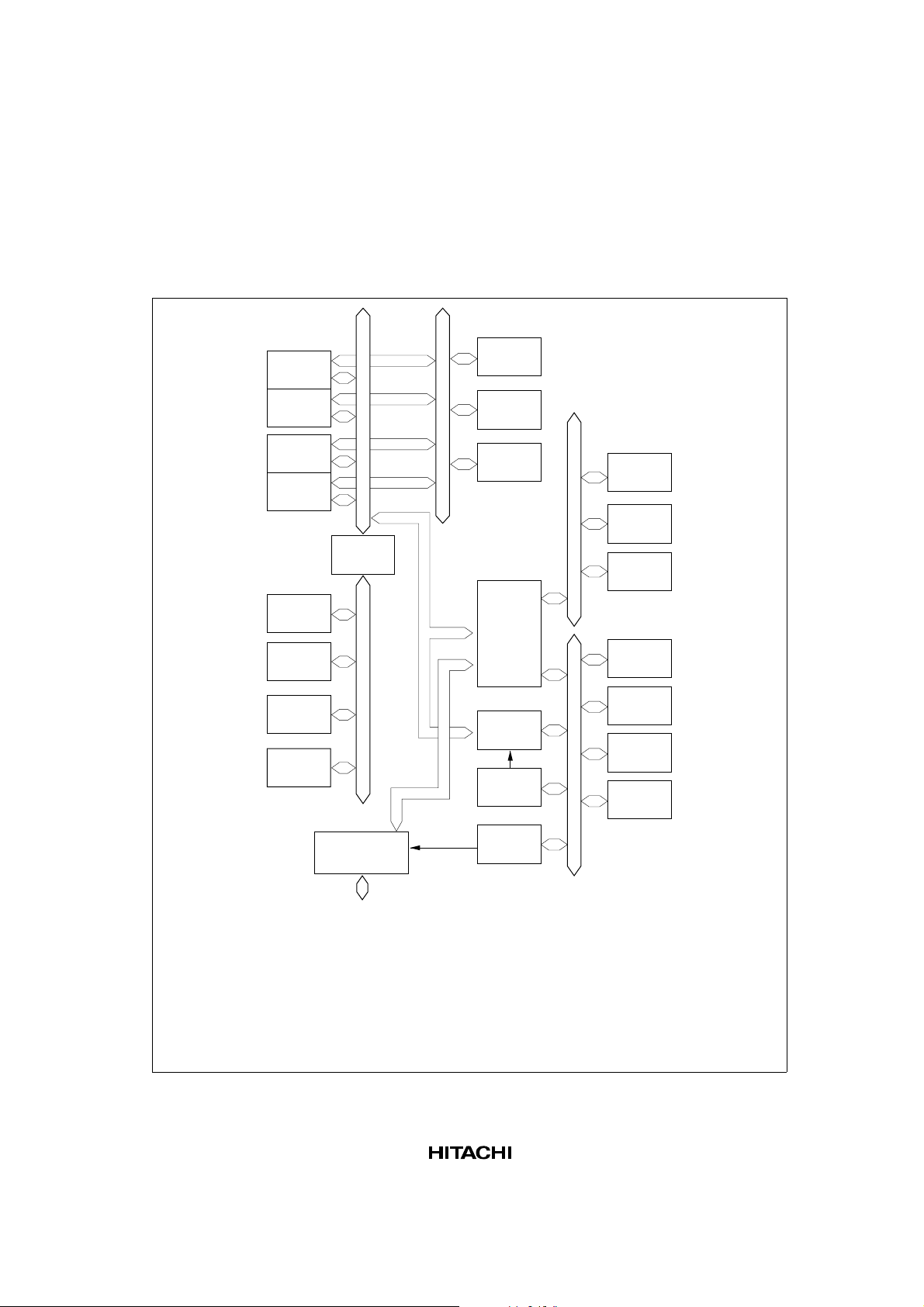
6
1.2 Block Diagram
MMU
TLB
SH-3
CPU
UBC
SCI
TMU
RTC
IrDA
SCIF
ADC
DAC
AUD
BRIDGE
DMAC
CMT
I/O port
External bus
interface
BSC
CCN
CACHE
ASERAM
UDI
INTC
CPG/WDT
Peripheral bus 1
Peripheral bus 2
L bus
I bus 1I bus 2
Legend:
ADC:
ASERAM:
AUD:
BSC:
CACHE:
CCN:
CMT:
CPG/WDT:
CPU:
DAC:
DMAC:
H-UDI:
A/D converter
ASE memory
Advanced user debugger
Bus state controller
Cache memory
Cache memory controller
Compare match timer
Clock pulse generator/watchdog timer
Central processing unit
D/A converter
Direct memory access controller
Hitachi user-debugging interface
INTC:
IrDA:
MMU:
RTC:
SCI:
SCIF:
TLB:
TMU:
UBC:
Interrupt controller
Serial communicatiion interface (with IrDA)
Memory management unit
Realtime clock
Serial communication interface (with smart card interface)
Serial communication interface (with FIFO)
Address translation buffer
Timer unit
User break controller
Figure 1.1 Block Diagram
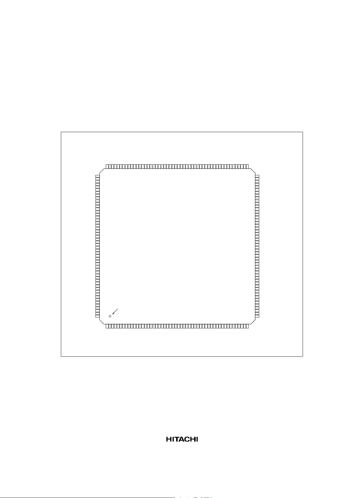
7
1.3 Pin Description
1.3.1 Pin Assignment
123456789101112131415161718192021222324252627282930313233343536373839404142434445464748495051
52
MD1
MD2
V
CC
-RTC
XTAL2
EXTAL2
V
SS
-RTC
NMI
IRQ0/IRL0/PTH[0]
IRQ1/IRL1/PTH[1]
IRQ2/IRL2/PTH[2]
IRQ3/IRL3/PTH[3]
IRQ4/PTH[4]
D31/PTB[7]
D30/PTB[6]
D29/PTB[5]
D28/PTB[4]
D27/PTB[3]
D26/PTB[2]
V
SS
Q
D25/PTB[1]
V
CC
Q
D24/PTB[0]
D23/PTA[7]
D22/PTA[6]
D21/PTA[5]
D20/PTA[4]
V
SS
D19/PTA[3]
V
CC
D18/PTA[2]
D17/PTA[1]
D16/PTA[0]
V
SS
Q
D15
V
CC
Q
D14
D13
D12
D11
D10
D9D8D7
D6
V
SS
Q
D5
V
CC
Q
D4D3D2D1D0
156
155
154
153
152
151
150
149
148
147
146
145
144
143
142
141
140
139
138
137
136
135
134
133
132
131
130
129
128
127
126
125
124
123
122
121
120
119
118
117
116
115
114
113
112
111
110
109
108
107
106
105
EXTAL
XTAL
V
CCVSSVSS
AUDCK/PTH[6]
V
CC
-PLL2
CAP2
V
SS
-PLL2
V
SS
-PLL1
CAP1
V
CC
-PLL1
MD0
IRLS0/PTF[0]/PINT[8]
IRLS1/PTF[1]/PINT[9]
IRLS2/PTF[2]/PINT[10]
IRLS3/PTF[3]/PINT[11]
TCK/PTF[4]/PINT[12]
TDI/PTF[5]/PINT[13]
TMS/PTF[6]/PINT[14]
TRST/PTF[7]/PINT[15]
AUDATA[0]/PTG[0]
V
CC
AUDATA[1]/PTG[1]
VSSAUDATA[2]/PTG[2]
AUDATA[3]/PTG[3]
PTG[4]/CKIO2
ASEBRKAK/PTG[5]
ASEMD0/PTG[6]
IOIS16/PTG[7]
ADTRG/PTH[5]
RESETM
WAIT
BREQ
BACK
TDO/PTE[0]
PTE[1]
RAS3U/PTE[2]
PTE[3]
PTE[6]
DACK1/PTD[7]
DACK0/PTD[5]
PTJ[5]
PTJ[4]
V
CC
Q
CASU/PTJ[3]
V
SS
Q
CASL/PTJ[2]
PTJ[1]
RAS3L/PTJ[0]
CKE/PTK[5]
157
158
159
160
161
162
163
164
165
166
167
168
169
170
171
172
173
174
175
176
177
178
179
180
181
182
183
184
185
186
187
188
189
190
191
192
193
194
195
196
197
198
199
200
201
202
203
204
205
206
207
208
STATUS0/PTJ[6]
STATUS1/PTJ[7]
TCLK/PTH[7]
IRQOUT
V
SS
Q
CKIO
V
CC
Q
TxD0/SCPT[0]
SCK0/SCPT[1]
TxD1/SCPT[2]
SCK1/SCPT[3]
TxD2/SCPT[4]
SCK2/SCPT[5]
RTS2/SCPT[6]
RxD0/SCPT[0]
RxD1/SCPT[2]
V
SS
RXD2/SCPT[4]
V
CC
CTS2/IRQ5/SCPT[7]
MCS[7]/PTC[7]/PINT[7]
MCS[6]/PTC[6]/PINT[6]
MCS[5]/PTC[5]/PINT[5]
MCS[4]/PTC[4]/PINT[4]
V
SS
Q
WAKEUP/PTD[3]
V
CC
Q
RESETOUT/PTD[2]
MCS[3]/PTC[3]/PINT[3]
MCS[2]/PTC[2]/PINT[2]
MCS[1]/PTC[1]/PINT[1]
MCS[0]/PTC[0]/PINT[0]
DRAK0/PTD[1]
DRAK1/PTD[0]
DREQ0/PTD[4]
DREQ1/PTD[6]
RESETP
CA
MD3
MD4
MD5
AV
SS
AN[0]/PTL[0]
AN[1]/PTL[1]
AN[2]/PTL[2]
AN[3]/PTL[3]
AN[4]/PTL[4]
AN[5]/PTL[5]
AV
CC
AN[6]/DA[1]/PTL[6]
AN[7]/DA[0]/PTL[7]
AV
SS
104
103
102
101
100
99
98
97
96
95
94
93
92
91
90
89
88
87
86
85
84
83
82
81
80
79
78
77
76
75
74
73
72
71
70
69
68
67
66
65
64
63
62
61
60
59
58
57
56
55
54
53
CE2B/PTE[5]
CE2A/PTE[4]
CS6/CE1B
CS5/CE1A/PTK[3]
CS4/PTK[2]
CS3/PTK[1]
CS2/PTK[0]
V
CC
Q
CS0/MCS0
V
SS
Q
AUDSYNC/PTE[7]
RD/WR
WE3/DQMUU/ICIOWR/PTK[7]
WE2/DQMUL/ICIORD/PTK[6]
WE1/DOMLU/WE
WE0/DQMLL
RD
BS/PTK[4]
A25
V
CC
Q
A24
V
SS
Q
A23
V
CC
A22
V
SS
A21
A20
A19
A18
A17
A16
A15
V
CC
Q
A14
V
SS
Q
A13
A12
A11
A10
A9
A8
A7
A6
A5
V
CC
Q
A4
V
SS
Q
A3
A2
A1
A0
SH7709S
FP-208C
FP-208E
(Top view)
INDEX MARK
Figure 1.2 Pin Assignment (FP-208C, FP-208E)
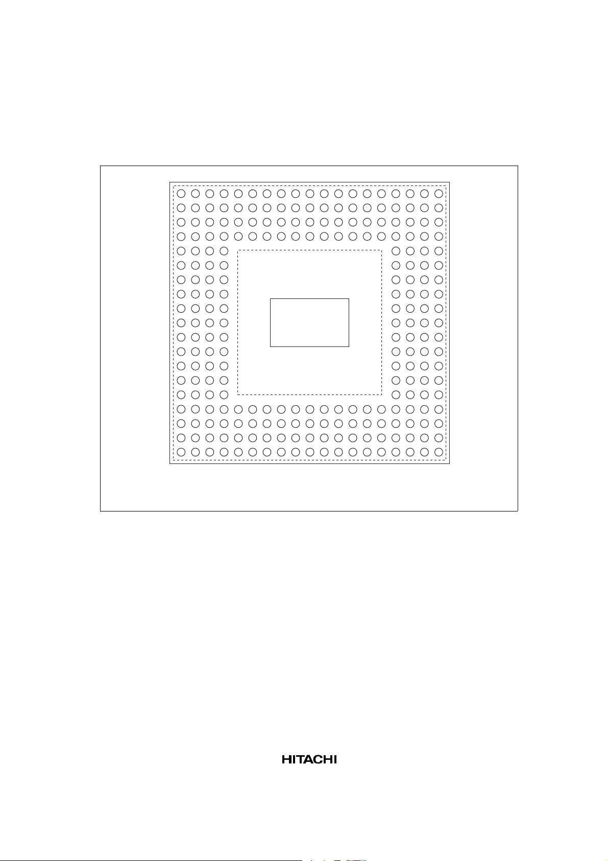
8
19
18
17
16
15
14
13
12
11
10
9
8
7
6
5
4
3
2
1
19
18
17
16
15
14
13
12
11
10
9
8
7
6
5
4
3
2
1
ABCDEFGHJKLMNPRTUVW
ABCDEFGHJKLMNPRTUVW
Note: The pin area enclosed in broken lines is an inner view.
SH7709S
BP-240A
(Top view)
Figure 1.3 Pin Assignment (BP-240A)

9
1.3.2 Pin Function
Table 1.3 SH7709S Pin Function
Number of Pins
FP-208C
FP-208E
BP-240A Pin Name I/O Description
1 D2 MD1 I Clock mode setting
2 C2 MD2 I Clock mode setting
3 E2 Vcc-RTC
*1
— RTC power supply (*4)
4 D1 XTAL2 O On-chip RTC crystal oscillator pin
5 D3 EXTAL2 I On-chip RTC crystal oscillator pin
6 E1 Vss-RTC
*1
— RTC power supply (0 V)
7 C3 NMI I Nonmaskable interrupt request
8 E3 IRQ0/IRL0/PTH[0] I External interrupt request/input
port H
9 E4 IRQ1/IRL1/PTH[1] I External interrupt request/input
port H
10 F1 IRQ2/IRL2/PTH[2] I External interrupt request/input
port H
11 F2 IRQ3/IRL3/PTH[3] I External interrupt request/input
port H
12 F3 IRQ4/PTH[4] I External interrupt request/input
port H
13 F4 D31/PTB[7] I/O Data bus / input/output port B
14 G1 D30/PTB[6] I/O Data bus / input/output port B
15 G2 D29/PTB[5] I/O Data bus / input/output port B
16 G3 D28/PTB[4] I/O Data bus / input/output port B
17 G4 D27/PTB[3] I/O Data bus / input/output port B
18 H1 D26/PTB[2] I/O Data bus / input/output port B
19 H2 VssQ — Input/output power supply (0 V)
20 H3 D25/PTB[1] I/O Data bus / input/output port B
21 H4 VccQ — Input/output power supply (3.3 V)
22 J1 D24/PTB[0] I/O Data bus / input/output port B
23 J2 D23/PTA[7] I/O Data bus / input/output port A
24 J4 D22/PTA[6] I/O Data bus / input/output port A
25 J3 D21/PTA[5] I/O Data bus / input/output port A

10
Table 1.3 SH7709S Pin Function (cont)
Number of Pins
FP-208C
FP-208E
BP-240A Pin Name I/O Description
26 K2 D20/PTA[4] I/O Data bus / input/output port A
27 K3 Vss — Power supply (0 V)
— K4 Vss — Power supply (0 V)
28 K1 D19/PTA[3] I/O Data bus / input/output port A
29 L3 Vcc — Power supply (1.9 V/1.8 V*4)
— L4 Vcc — Power supply (*4)
30 L2 D18/PTA[2] I/O Data bus / input/output port A
31 L1 D17/PTA[1] I/O Data bus / input/output port A
32 M4 D16/PTA[0] I/O Data bus / input/output port A
33 M3 VssQ — Input/output power supply (0 V)
34 M2 D15 I/O Data bus
35 M1 VccQ — Input/output power supply (3.3 V)
36 N4 D14 I/O Data bus
37 N3 D13 I/O Data bus
38 N2 D12 I/O Data bus
39 N1 D11 I/O Data bus
40 P4 D10 I/O Data bus
41 P3 D9 I/O Data bus
42 P2 D8 I/O Data bus
43 P1 D7 I/O Data bus
44 R4 D6 I/O Data bus
45 R3 VssQ — Input/output power supply (0 V)
46 T4 D5 I/O Data bus
47 R1 VccQ — Input/output power supply (3.3 V)
48 T3 D4 I/O Data bus
49 T1 D3 I/O Data bus
50 R2 D2 I/O Data bus
51 U2 D1 I/O Data bus
52 T2 D0 I/O Data bus
53 V4 A0 O Address bus

11
Table 1.3 SH7709S Pin Function (cont)
Number of Pins
FP-208C
FP-208E
BP-240A Pin Name I/O Description
54 V3 A1 O Address bus
55 V5 A2 O Address bus
56 W4 A3 O Address bus
57 U4 VssQ — Input/output power supply (0 V)
58 W5 A4 O Address bus
59 U3 VccQ — Input/output power supply (3.3 V)
60 U5 A5 O Address bus
61 T5 A6 O Address bus
62 W6 A7 O Address bus
63 V6 A8 O Address bus
64 U6 A9 O Address bus
65 T6 A10 O Address bus
66 W7 A11 O Address bus
67 V7 A12 O Address bus
68 U7 A13 O Address bus
69 T7 VssQ — Input/output power supply (0 V)
70 W8 A14 O Address bus
71 V8 VccQ — Input/output power supply (3.3 V)
72 U8 A15 O Address bus
73 T8 A16 O Address bus
74 W9 A17 O Address bus
75 V9 A18 O Address bus
76 T9 A19 O Address bus
77 U9 A20 O Address bus
78 V10 A21 O Address bus
79 U10 Vss — Power supply (0 V)
— T10 Vss O Power supply (0 V)
80 W10 A22 O Address bus
81 U11 Vcc — Power supply (*4)
— T11 Vcc — Power supply (*4)
 Loading...