

HITACHI PF08103A Datasheet

PF08103A
MOS FET Power Amplifier Module
for E-GSM900 and DCS1800 Dual Band Handy Phone
ADE-208-685B (Z)
Application
• Dual band amplifier for E-GSM900 (880 to 915 MHz) and DCS1800 (1710 to 1785 MHz).
• For 4.8 V nominal battery use
Features
• 1 in / 2 out dual band amplifier
• Simple external circuit including output matching circuit
• Simple band switching and power control
• High gain 3stage amplifier : +4.5 dBm input
• Lead less thin & Small package : 11 × 13.75 × 1.8 mm
• High efficiency : 48% Typ at 34.5 dBm for E-GSM
36% Typ at 31.5 dBm for DCS1800
3rd Edition
Apr. 1999
PF08103A
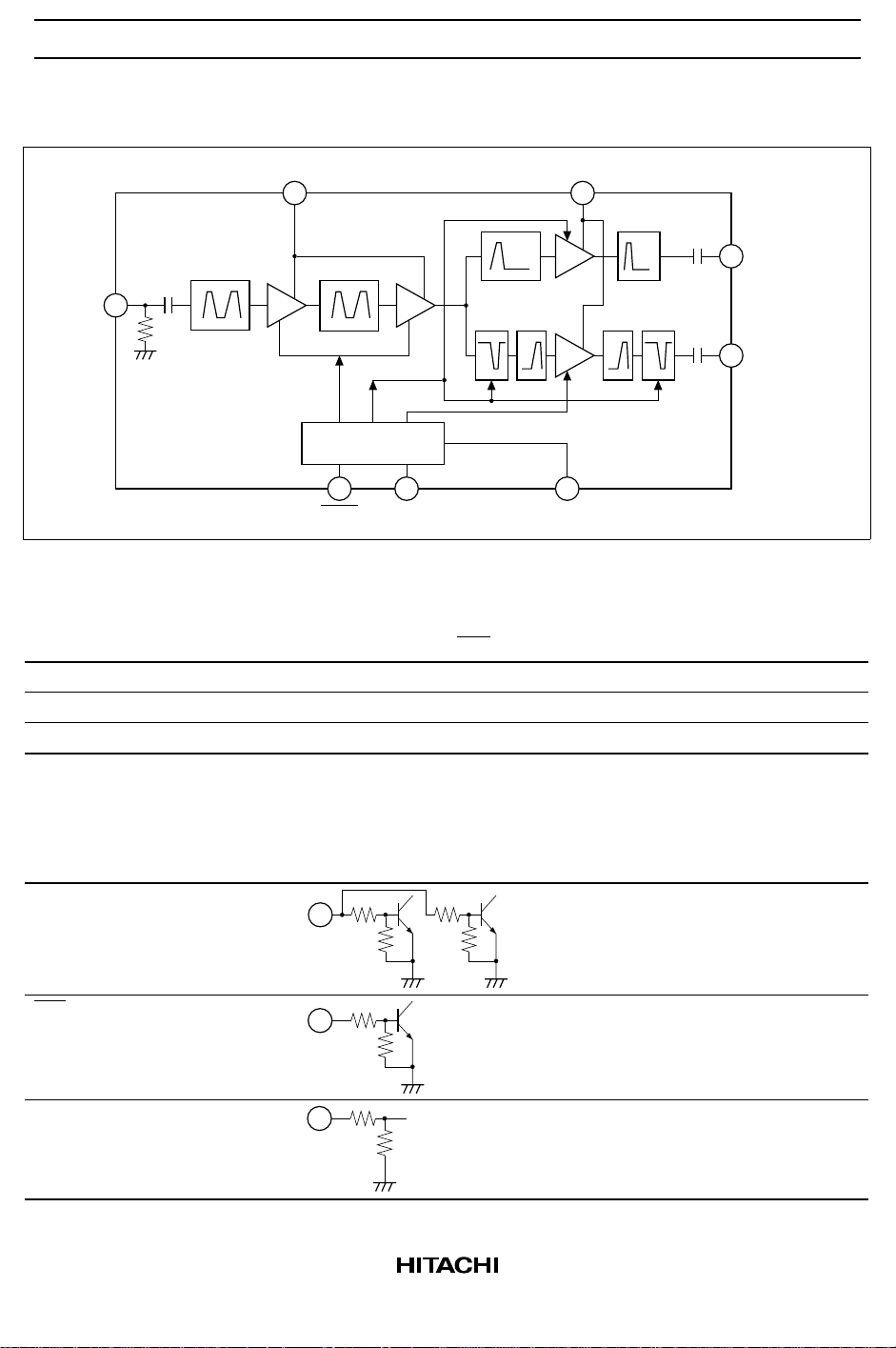
Internal Circuit Block Diagram
Vdd1
Vdd2
Pin
Bias circuit
V
CTL
V
CTL
Vapc
Band Select and Power Control (H: 2 V Min, L: 0.3 V Max)
Operating Mode V
CTL
GSM Tx ON H L Control
DCS Tx ON L H Control
Tx OFF L L < 0.2 V
V
CTL
Vapc
Pout
Pout
GSM
DCS
Current of Control Pin
Control Pin Equivalent Input Circuit Control Current
V
CTL
V
CTL
Vapc 3 mA Max at 3 V
2
160 µA Max at 3 V
80 µA Max at 3 V
Internal Diagram and External Circuit
8
Pin
Z1 Z2
Bias circuit
4
Pout
5
Pout
PF08103A
GSM
DCS
Z3
3
C2
Pin
C1
6
V
C3
CTL
V
CTL
C5
FB
V
CTL
V
CTL
721
Vapc Vdd2Vdd1
C6 C7 C4
FB FB
Vapc Vdd2Vdd1
Note: C1 = C2 = 4.7 µF TANTALUM ELECTROLYTE
C3 = C4 = 0.01 µF CERAMIC CHIP
C5 = C6 = C7 = 1000 pF CERAMIC CHIP
FB = FERRITE BEAD BLO1RN1-A62-001 (MURATA) or equivalent
Z1 = Z2 = Z3 = 50 Ω MICRO STRIP LINE
Pout
DCS
Pout
GSM
3
 Loading...