HITACHI PF0030 Datasheet
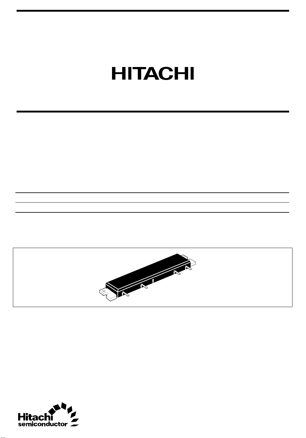
PF0030 Series
MOS FET Power Amplifier
Features
• High stability: Load VSWR = 20 : 1
• Low power control current: 400 µA
• Thin package: 5 mmt
Ordering Information
Type No Operating Frequency Application
PF0030 824 to 849 MHz AMPS
PF0032 872 to 905 MHz E-TACS
ADE-208-460 (Z)
1st Edition
July 1996
Pin Arrangement
• RF-B2
5
1: Pin
2: V
4
3
2
5
1
APC
3: V
DD
4: Pout
5: GND
PF0030 Series
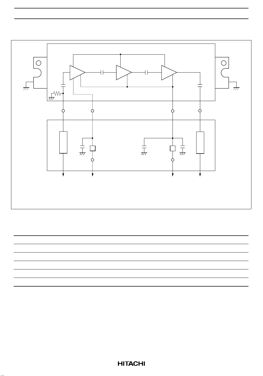
Internal Diagram and External Circuit
G
GND
Pin1
Pin
Z1
C1 C3 C2
Pin
Pin2
V
APC
FB1 FB2
V
APC
Pin3
V
DD
Pin4
Pout
V
DD
Pout
C1 = C2 = 0.01 µF (Ceramic chip capacitor)
C3 = 10 µF (Aluminum Electrolyte Capacitor)
FB = Ferrite bead BL01RN1-A62-001 (Manufacture: MURATA) or equivalent
Z1 = Z2 = 50 Ω (Microstrip line)
Absolute Maximum Ratings (Ta = 25°C)
Item Symbol Rating Unit
Supply voltage V
Supply current I
APC voltage V
DD
DD
APC
Input power Pin 20 mW
Operating case temperature Tc (op) –30 to +110 °C
Storage temperature Tstg –40 to +110 °C
17 V
3A
±8V
G
GND
Z2
2
PF0030 Series
Electrical Characteristics (Ta = 25°C)
Item Symbol Min Typ Max Unit Test Condition
Drain cutoff current I
Total efficiency η
DS
T
— — 500 µAVDD = 17 V, V
35 40 — % Pin = 2 mW,
2nd harmonic distortion 2nd H.D. — –50 –30 dB VDD = 12.5 V,
3rd harmonic distortion 3rd H.D. — –50 –30 dB Pout = 6 W (at APC controlled)
Input VSWR VSWR (in) — 1.5 3 — Zin = Zout = 50 Ω
Output VSWR VSWR (out) — 1.5 — —
Stability — No parasitic oscillation — Pin = 2 mW, VDD = 12.5 V,
Pout = 6 W (at APC controlled),
Zin = 50 Ω,
Output VSWR = 20:1 All phases,
t = 20 sec
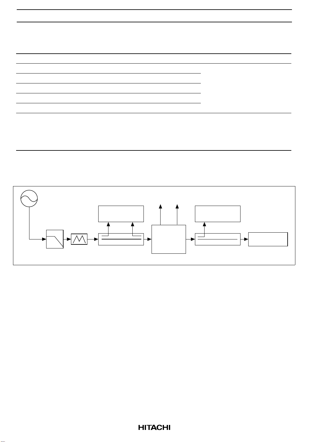
Test System Diagram
APC
= 0 V
S.G
L.P.F
3dB
ATT
Power
Meter
Directional
Coupler
V
APCVDD
Test
Fixture
Spectrum
Analyzer
Power Meter
Directional
Coupler
3
PF0030 Series
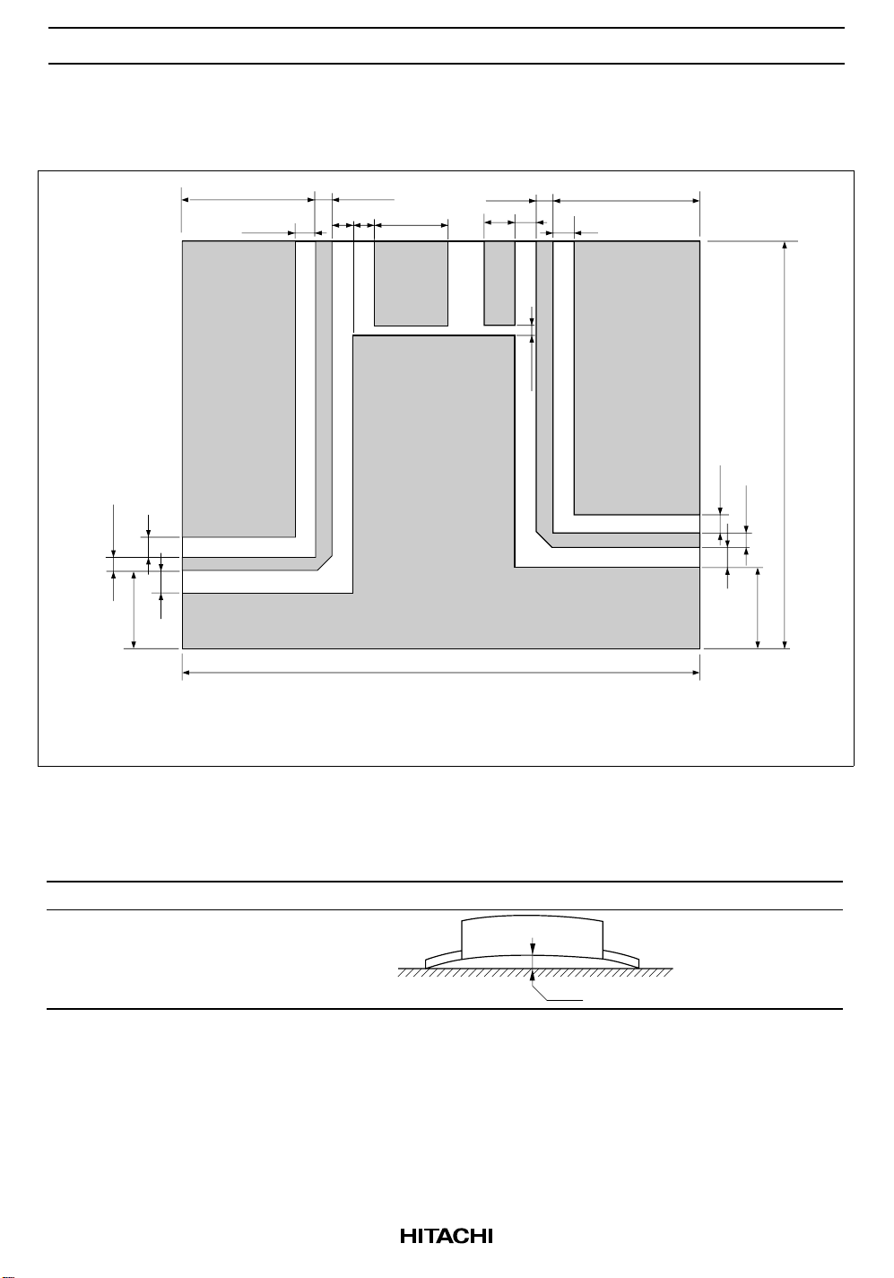
Test Fixture Pattern
Unit: mm
2.88
15
26.5
3.5
4
4
4.5
2.88
3
V
APC
16
100
2.88
6
V
DD
4
1.5
28
4
80
3.5
2.88
4
16.5
Grass Epoxy Double sided PCB
(t = 1.6 mm, εr = 4.8)
Mechanical Characteristics
Item Conditions Spec
Torque for screw up the heatsink flange M3 Screw Bolts 4 to 6 kg•cm
Warp size of the heatsink flange: S
S
S = 0
+0.3/–0 mm
4

PF0030 Series
Note for Use
• Unevenness and distortion at the surface of the heatsink attached module should be less than 0.05 mm.
• It should not be existed any dust between module and heatsink.
• MODULE should be separated from PCB less than 1.5 mm.
• Soldering temperature and soldering time should be less than 230°C, 10 sec.
(Soldering position spaced from the root point of the lead frame: 2 mm)
• Recommendation of thermal joint compounds is TYPE G746.
(Manufacturer: Shin-Etsu Chemical, Co., Ltd.)
• To protect devices from electro-static damage, soldering iron, measuring-equipment and human body etc.
should be grounded.
• Torque for screw up the heatsink flange should be 4 to 6 kg · cm with M3 screw bolts.
• Don’t solder the flange directly.
• It should make the lead frame as straight as possible.
• The module should be screwed up before lead soldering.
• It should not be given mechanical and thermal stress to lead and flange of the module.
• When the external parts (Isolator, Duplexer, etc.) of the module are changed, the electrical characteristics
should be evaluated enough.
• Don’t washing the module except lead pins.
• To get good stability, ground impedance between the module GND flange and PCB GND pattern should
be designed as low as possible.
5
PF0030 Series
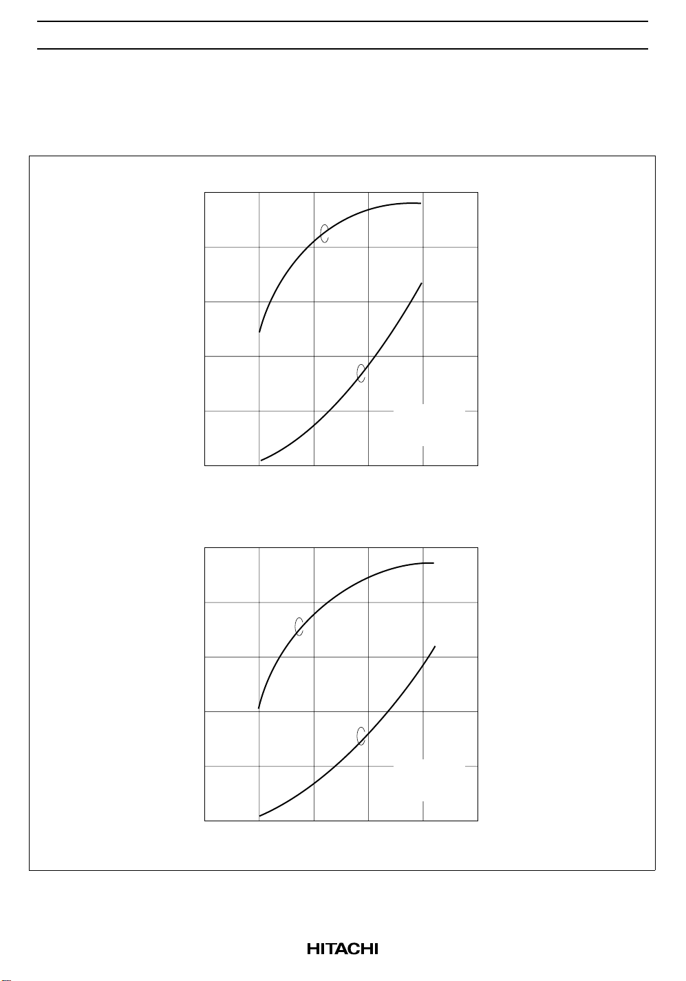
Characteristics Curve
PF0030
20
16
Pout, ηT vs. VDD (1)
η
T
50
40
12
8
Pout
Output Power Pout (W)
4
f = 824 MHz
Pin = 2 mW
V
APC
0
0 4 8 12 16 20
Supply Voltage VDD (V)
Pout, ηT vs. VDD (2)
20
16
η
T
12
= 4 V
30
20
10
0
50
40
30
(%)
T
Efficiency η
(%)
T
8
Pout
20
Efficiency η
Output Power Pout (W)
4
f = 849 MHz
10
Pin = 2 mW
V
= 4 V
APC
0
0
0 4 8 12 16 20
Supply Voltage VDD (V)
6
 Loading...