

Page 1

MAY 2001 HHEA-MANUFACTURING DIVISION
PA
No. 0146
43FDX10B 43FDX11B
53UDX10B 61UDX10B
R/C: CLU-5711TSI
CLU-5713TSI
NNTTSSCC
DDPP1155 DDPP1155EE
CChhaassssiiss
SERVICE MANUAL
CONTENTS
IMPORTANT SAFETY INSTRUCTIONS . . . . . . . . . . . . . . . . . . . . . . . . . . . . . . . . . . . 2
SERVICING PRECAUTIONS . . . . . . . . . . . . . . . . . . . . . . . . . . . . . . . . . . . . . . . . . . . . 6
TECHNICAL CAUTIONS . . . . . . . . . . . . . . . . . . . . . . . . . . . . . . . . . . . . . . . . . . . . . . 10
SPECIFICATIONS . . . . . . . . . . . . . . . . . . . . . . . . . . . . . . . . . . . . . . . . . . . . . . . . . . . 11
CIRCUIT PROTECTION . . . . . . . . . . . . . . . . . . . . . . . . . . . . . . . . . . . . . . . . . . . . . . 11
CAUTIONS WHEN CONNECTING/DISCONNECTING THE HV CONNECTOR . . . . . .12
GENERAL INFORMATION . . . . . . . . . . . . . . . . . . . . . . . . . . . . . . . . . . . . . . . . . . . . .13
REMOTE CONTROL . . . . . . . . . . . . . . . . . . . . . . . . . . . . . . . . . . . . . . . . . . . . . . . . .14
CUSTOMIZED PICTURE AND SOUND ADJUSTMENTS . . . . . . . . . . . . . . . . . . . . . .15
REAR PANEL CONNECTION . . . . . . . . . . . . . . . . . . . . . . . . . . . . . . . . . . . . . . . . . . .17
DISPLAY PICTURE FORMATS . . . . . . . . . . . . . . . . . . . . . . . . . . . . . . . . . . . . . . . . . .22
SERVICE ADJUSTMENTS . . . . . . . . . . . . . . . . . . . . . . . . . . . . . . . . . . . . . . . . . . . . .30
TROUBLESHOOTING . . . . . . . . . . . . . . . . . . . . . . . . . . . . . . . . . . . . . . . . . . . . . . . .64
WAVEFORMS . . . . . . . . . . . . . . . . . . . . . . . . . . . . . . . . . . . . . . . . . . . . . . . . . . . . . .67
DC VOLTAGE TABLES . . . . . . . . . . . . . . . . . . . . . . . . . . . . . . . . . . . . . . . . . . . . . . . .71
PROTECTION CIRCUIT BLOCK DIAGRAM . . . . . . . . . . . . . . . . . . . . . . . . . . . . . . . .81
BASIC CIRCUIT DIAGRAM . . . . . . . . . . . . . . . . . . . . . . . . . . . . . . . . . . . . . . . . . . . .83
PRINTED CIRCUIT BOARDS . . . . . . . . . . . . . . . . . . . . . . . . . . . . . . . . . . . . . . . . . . .98
BLOCK DIAGRAM . . . . . . . . . . . . . . . . . . . . . . . . . . . . . . . . . . . . . . . . . . . . . . . . . .110
WIRING DIAGRAM . . . . . . . . . . . . . . . . . . . . . . . . . . . . . . . . . . . . . . . . . . . . . . . . . .111
CHASSIS WIRING DRAWING . . . . . . . . . . . . . . . . . . . . . . . . . . . . . . . . . . . . . . . . .112
EXPLODED VIEW . . . . . . . . . . . . . . . . . . . . . . . . . . . . . . . . . . . . . . . . . . . . . . . . . .116
REPLACEMENT PARTS LIST . . . . . . . . . . . . . . . . . . . . . . . . . . . . . . . . . . . . . . . . . .119
QUICK REFERENCE PARTS LIST . . . . . . . . . . . . . . . . . . . . . . . . . . . . . . . . . . . . . .148
CAUTION: These servicing instructions are for use by qualified service personnel only. To reduce the risk of
electric shock do not perform any servicing other than that contained in the operating instructions
unless you are qualified to do so. Before servicing this chassis, it is important that the service
technician read the “IMPORTANT SAFETY INSTRUCTIONS” in this service manual.
SAFETY NOTICE
USE ISOLATION TRANSFORMER WHEN SERVICING
Components having special safety characteristics are identified by a on the schematics and on the parts list in this
Service Data and its supplements and bulletins. Before servicing the chassis, it is important that the service technician
PROJECTION COLOR TELEVISION
SPECIFICATIONS AND PARTS ARE SUBJECT TO CHANGE FOR IMPROVEMENT
!
Page 2

2
Components having special safety characteristics are identified by a on the schematics and on the parts list in this service
manual and its supplements and bulletins. Before servicing this chassis, it is important that the service technician read and
follow the “Important Safety Instructions” in this Service Manual.
For continued X-Radiation protection, replace picture tube with original type or Hitachi approved equivalent type.
This Service Manual is intended for qualified service technicians; it is not meant for the casual do-it-yourselfer. Qualified
technicians have the necessary test equipment and tools, and have been trained to properly and safely repair complex
products such as those covered by this manual.
Improperly performed repairs can adversely affect the safety and reliability of the product and may void warranty. If you
are not qualified to perform the repair of this product properly and safely, you should not risk trying to do so and refer the
repair to a qualified service technician.
WARNING
Lead in solder used in this product is listed by the California Health and Welfare agency as a known reproductive toxicant which
may cause birth defects or other reproductive harm (California Health and Safety Code, Section 25249.5).
When servicing or handling circuit boards and other components which contain lead in solder, avoid unprotected skin contact
with solder. Also, when soldering do not inhale any smoke or fumes produced.
This television receiver provides display of television closed captioning in accordance with section 15.119 of the FCC rules.
FEDERAL COMMUNICATIONS COMMISSION NOTICE
This equipment has been tested and found to comply with the limits for a Class B digital device, pursuant to Part 15 of the
FCC Rules. These limits are designed to provide reasonable protection against harmful interference in a residential
installation. This equipment generates, uses, and can radiate radio frequency energy and, if not installed and used in
accordance with the instructions, may cause harmful interference to radio communications. However, there is no guarantee
that interference will not occur in a particular installation. If this equipment does cause harmful interference to radio or
television reception, which can be determined by turning the equipment off and on, the user is encouraged to try to correct
the interference by one or more of the following measures:
¥ Reorient or relocate the receiving antenna.
¥ Increase the separation between the equipment and the receiver.
¥ Connect the equipment into an outlet on a circuit different from that to which the receiver is connected.
¥ Consult the dealer or an experienced radio/television technician for help.
IMPORTANT SAFETY INSTRUCTIONS
USE ISOLATION TRANSFORMER WHEN SERVICING
!
Page 3
3
IMPORTANT SAFETY INSTRUCTION
1. Before returning an instrument to the customer, always
make a safety check of the entire instrument, including
but not limited to the following items.
a. Be sure that no built-in protective devices are
defective and/or have been deleted during servicing.
(1) Protective shields are provided on this chassis to
protect both the technician and the customer.
Correctly replace all missing protective shields,
including any removed for servicing convenience. (2)
When reinstalling the chassis and/or other assembly
in the cabinet, be sure to put back in place all
protective devices, including but not limited to,
nonmetallic control knobs, insulating fishpaper,
adjustment and compartment covers/shields, and
isolation resistor/capacitor networks. Do not operate
this instrument or permit it to be operated without
all protective devices correctly installed and
functioning. Servicers who defeat safety features
or fail to perform safety checks may be liable for
any resulting damage.
b. Be sure that there are no cabinet openings through
which an adult or child might be able to insert their
fingers and contact a hazardous voltage. Such
openings include, but are not limited to (1) spacing
between the picture tube and cabinet mask, (2)
excessively wide cabinet ventilation slots, and (3) an
improperly fitted and/or incorrectly secured cabinet
back cover.
c. Antenna Cold Check Ð With the instrument AC plug
removed from any AC source, connect an electrical
jumper across the two AC plug prongs. Place the
instrument AC switch in the on position. Connect one
lead of an ohmmeter to the AC plug prongs tied
together and touch the other ohmmeter lead in turn to
each tuner antenna input, exposed terminal screw
and, if applicable, to the coaxial connector. If the
measured resistance is less than 1.0 megohms or
greater than 5.2 megohms, an abnormality exists that
must be corrected before the instrument is returned to
the customer. Repeat this test with the instrument AC
switch in the off position.
d. Leakage Current Hot Check Ð With the instrument
completely reassembled, plug the AC line cord
directly into a 120V AC outlet. (Do not use an isolation
transformer during this test.) Use a leakage current
tester or a metering system that complies with
American National Standards Institute (ANSI) C101.0
Leakage Current for Appliances and Underwriters
Laboratories (UL) 1410, (50.7). With the instrument
AC switch first in the on position and then in the off
position, measure from a known earth ground (metal
waterpipe, conduit, etc.) to all exposed metal parts of
the instrument (antennas, handle bracket, metal
cabinet, screw heads, metallic overlays, control
shafts, etc.), especially any exposed metal parts that
offer an electrical return path to the chassis. Any
current measured must not exceed 0.5 milliamps.
Reverse the instrument power cord plug in the outlet
and repeat test.
ANY MEASUREMENTS NOT WITHIN THE LIMITS
SPECIFIED HEREIN INDICATE A POTENTIAL
SHOCK HAZARD THAT MUST BE ELIMINATED
BEFORE RETURNING THE INSTRUMENT TO THE
CUSTOMER OR BEFORE CONNECTING THE
ANTENNA OR ACCESSORIES.
e. High Voltage — This receiver is provided with a hold
down circuit for clearly indicating that voltage has
increased in excess of a predetermined value.
Comply will all notes described in this Service Manual
regarding this hold down circuit when servicing, so
that this hold down circuit may correctly be operated.
f. Service Warning — With maximum contrast, operating
high voltage in this receiver is lower than 31.5 kV. In
case any component having influence on high voltage
is replaced, confirm that the high voltage with
maximum contrast is lower than 31.5 kV.
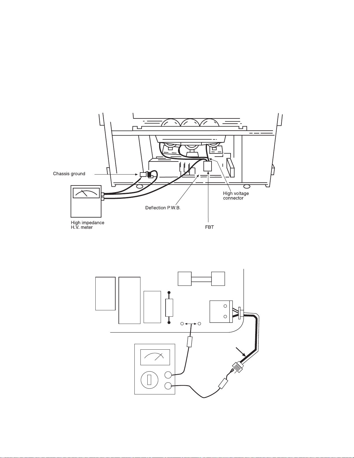
To measure H.V. use a high impedance H.V. meter.
Connect (-) to chassis earth and (+) to the CRT anode
button. (See the following connection diagram.)
Note: Turn power switch off without fail before the
connection to the anode button is made.
LEAKAGE
CURRENT
TESTER
(READING
SHOULD NOT
BE ABOVE 0.5mA)
EARTH
GROUND
TEST ALL
EXPOSED
METAL SURFACES
DEVICE
UNDER
TEST
2-WIRE CORD
ALSO TEST WITH PLUG
REVERSED
(USING AC ADAPTER
PLUS AS REQUIRED)
AC Leakage Test
Chassis
ground
FBT
High Impedance
H.V. meter
Deflection P.W.B.
(TH01)
High voltage
connector
Page 4
4
g. X-radiation – TUBE: The primary source of X-
radiation in this receiver is the picture tube. The tube
utilized for the above mentioned function in this
chassis is specially constructed to limit X-radiation
emissions.
For continued X-radiation protection, the replacement
tube must be the same type as the original, Hitachi
approved type.
When troubleshooting and making test measurements in a receiver with a problem of excessive high
voltage, avoid being unnecessarily close to the picture tube and the high voltage component.
Do not operate the chassis longer than is necessary
to locate the cause of excessive voltage.
h. X-radiation Shield –
1. This receiver is provided with X-ray shield plates
for protection against X-radiation. Do not remove
X-ray shield plates A, B, or C shown in Fig. 1
unnecessarily, when troubleshooting and/or
making test measurements.
2. To prevent X-radiation, after replacement of
picture tube and lens, confirm these components
to be fixed correctly to bracket and cabinet, and
not to be taken off easily.
Shield Plate A
Glass Lens for Shielding
Shield Plate B
Shield Plate C
Shield Plate D
Detailing X-radiation shield
Shield Plate C
Fig. 1. Installation of shield lens, shield cover and shield plates (oblique view).
IMPORTANT SAFETY INSTRUCTIONS
Page 5

5
2. Read and comply with all caution and safety-related
notes on or inside the receiver cabinet, on the
receiver chassis, or on the picture tube.
3. Design Alteration Warning – Do not alter or add to
the mechanical or electrical design of this TV receiver.
Design alterations and additions including but not
limited to circuit modifications and the addition of
items such as auxiliary audio and/or video output
connectors, might alter the safety characteristics of
this receiver and create a hazard to the user. Any
design alterations or additions may void the
manufacturer’s warranty and may make you, the
servicer, responsible for personal injury or property
damage resulting therefrom.
4. Picture Tube Implosion Protection Warning – The
picture tube in this receiver employs integral
implosion protection. For continued implosion
protection, replace the picture tube only with one of
the same type number. Do not remove, install, or
otherwise handle the picture tube in any manner
without first putting on shatterproof goggles equipped
with side shields. People not so equipped must be
kept safely away while picture tubes are handled.
Keep the picture tube away from your body. Do not
handle the picture tube by its neck.
5. Hot Chassis Warning – a. Some TV receiver chassis
are electrically connected directly to one conductor of
the AC power cord and may be safely serviced
without an isolation transformer only if the AC power
plug is inserted so that the chassis is connected to the
ground side of the AC power source. Confirm that the
AC power plug is inserted correctly with an AC
voltmeter by measuring between the chassis and a
known earth ground. If a voltage reading in excess of
1.0V is obtained, remove and reinsert the AC power
plug in the opposite polarity and again measure the
voltage potential between the chassis and a known
earth ground. b. Some TV receiver chassis normally
have 85V AC (RMS) between chassis and earth
ground regardless of the AC plug polarity. These
chassis can be safely serviced only with an isolation
transformer inserted in the power line between the
receiver and the AC power source, for both personnel
and test equipment protection. c. Some TV receiver
chassis have a secondary ground system in addition
to the main chassis ground. This secondary ground
system is not isolated from the AC power line. The two
ground systems are electrically separated by
insulating material that must not be defeated or
altered.
6. Observe original lead dress. Take extra care to assure
correct lead dress in the following areas: a. near
sharp edges, b. near thermally hot parts – be sure
that leads and components do not touch thermally hot
parts, c. the AC supply , d. high voltage and e. antenna
wiring. Always inspect in all areas for pinched, out-ofplate, or frayed wiring. Do not change spacing
between components and the printed circuit board.
Check AC power cord for damage.
7. Components, parts, and/or wiring that appear to have
overheated or are otherwise damaged should be
replaced with components, parts, or wiring that meet
original specifications. Additionally, determine the
cause of overheating and/or damage and, if
necessary, take corrective action to remove any
potential safety hazard.
8. PRODUCT SAFETY NOTICE – Many TV electrical
and mechanical parts have special safety-related
characteristics some of which are often not evident
from visual inspection, nor can the protection they
give necessarily be obtained by replacing them with
components rated for higher voltage, wattage, etc.
Parts that have special safety characteristics are
identified in Hitachi service data by shading on
schematics and by a in the parts list. Use of
substitute replacement that does not have the same
safety characteristics as the recommended replacement part in Hitachi service data parts list might
create shock, fire, and/or other hazards. Product
safety is under review continuously and new
instructions are issued whenever appropriate. For the
latest information, always consult the appropriate
current Hitachi service literature. A subscription to, or
additional copies of service literature may be obtained
at a nominal charge from Hitachi.
!
IMPORTANT SAFETY INSTRUCTIONS
Page 6

6
CAUTION: Before servicing instruments covered by this
service data and its supplements and addenda, read and
follow the “Important Safety Instructions” on page 3 of this
publication.
NOTE: If unforeseen circumstances create conflict between
the following servicing precautions and any of the safety
precautions on page 3 of this publication, always follow the
safety precautions. Remember: Safety First.
General Servicing Guidelines
1. Always unplug the instrument AC power cord from the AC
power source before:
a. Removing or reinstalling any component, circuit
board, module, or any other instrument assembly.
b. Disconnecting or reconnecting any instrument
electrical plug or other electrical connection.
c. Connecting a test substitute in parallel with an
electrolytic capacitor in the instrument.
CAUTION: A wrong part substitution or incorrect
polarity installation of electrolytic
capacitors may result in an explosion
hazard.
d. Discharging the picture tube anode.
2. T est high voltage only by measuring it with an appropriate
high voltage meter or other voltage measuring device
(DVM, FETVOM, etc.) equipped with a suitable high
voltage probe. Do not test high voltage by “drawing an
arc.” The H.V. Distribution Box has an internal 400MW
resistor (bleeder resistor) connected from the high
voltage to ground. After power is removed from the
instrument the high voltage will discharge through the
high voltage bleeder resistor. If the tubes have high
voltage after power is removed, then the bleeder resistor
is defective or the bleeder ground is disconnected.
3. Discharge the picture tube’s anode at any of the R, G, or
B outputs on the H.V. Distribution Box only by (a) first
connecting one end of an insulated clip lead to the
degaussing or kine aquadag grounding system shield at
the point where the picture tube socket ground lead is
connected, and then (b) touch the other end of the
insulated clip lead to the picture tube high voltage
distribution box R, G, or B output, using an insulated
handle to avoid personal contact with high voltage.
4. Do not spray chemicals on or near this instrument or any
of its assemblies.
5. Unless specified otherwise in these service data, clean
electrical contracts by applying the following mixture to
the contacts with a pipe cleaner, cotton-tipped stick or
comparable nonabrasive applicator: 10% (by volume)
Acetone and 90% (by volume) isopropyl alcohol (90%99% strength).
CAUTION: This is a flammable mixture. Unless
specified otherwise in these service data,
lubrication of contacts is not required.
6. Do not defeat any plug/socket B+ voltage interlocks with
which instruments covered by this service data might be
equipped.
7. Do not apply AC power to this instrument and/or any of its
electrical assemblies unless all solid-state device heatsinks are correctly installed.
8. Always connect the test instrument ground lead to the
appropriate instrument chassis ground before connecting
the test instrument positive lead. Always remove the test
instrument ground lead last.
9. Use with this instrument only the test fixtures specified in
this service data.
CAUTION: Do not connect the test fixture ground strap
to any heatsink in this instrument.
Electrostatically Sensitive (ES) Devices
Some semiconductor (solid state) devices can be damaged
easily by static electricity. Such components commonly are
called Electrostatically Sensitive (ES) Devices. Examples of
typical ES devices are integrated circuits and some fieldeffect transistors and semiconductor “chip” components. The
following techniques should be used to help reduce the
incidence of component damage caused by static electricity.
1. Immediately before handling any semiconductor
component or semiconductor-equipped assembly, drain
off any electrostatic charge on your body by touching a
known earth ground. Alternatively, obtain and wear a
commercially available discharging wrist strap device,
which should be removed for potential shock reasons
prior to applying power to the unit under test.
2. After removing an electrical assembly equipped with ES
devices, place the assembly on a conductive surface
such as aluminum foil, to prevent electrostatic charge
buildup or exposure of the assembly.
3. Use only a grounded-tip soldering iron to solder or
desolder ES devices.
4. Use only can anti-static type solder removal device.
Some solder removal devices not classified as “antistatic” can generate electrical charges sufficient to
damage ES device.
5. Do not use freon-propelled chemicals. These can
generate electrical charges sufficient to damage ES
devices.
6. Do not remove a replacement ES device from its
protective package until immediately before you are
ready to install it. (Most replacement ES devices are
packaged with leads electrically shorted together by
conductive foam, aluminum foil or comparable conductive
material.)
7. Immediately before removing the protective material from
the leads of a replacement ES device, touch the
protective material to the chassis or circuit assembly into
which the device will be installed.
CAUTION: Be sure no power is applied to the chassis or
circuit, and observe all other safety
precautions.
8. Minimize bodily motions when handling unpackaged
replacement ES devices. (Otherwise harmless motion
such as the brushing together of your clothes fabric or the
lifting of your foot from a carpeted floor can generate
SERVICING PRECAUTIONS
Page 7
7
General Soldering Guidelines
1. Use a grounded-tip, low-wattage soldering iron and
appropriate tip size and shape that will maintain tip
temperature within the range 500°F to 600°F.
2. Use an appropriate gauge of resin-core solder composed
of 60 parts tin/40 parts lead.
3. Keep the soldering iron tip clean and well-tinned.
4. Thoroughly clean the surfaces to be soldered. Use a
small wire-bristle (0.5 inch or 1.25 cm) brush with a metal
handle. Do not use freon-propelled spray-on cleaners.
5. Use the following desoldering technique.
a. Allow the soldering iron tip to reach normal
temperature (500°F to 600°F).
b. Heat the component lead until the solder melts.
Quickly draw away the melted solder with an antistatic, suction-type solder removal device or with
solder braid.
CAUTION: Work quickly to avoid overheating the
circuit board printed foil.
6. Use the following soldering technique.
a. Allow the soldering iron tip to reach normal
temperature (500°F to 600°F).
b. First, hold the soldering iron tip and solder strand
against the component lead until the solder melts.
c. Quickly move the soldering iron tip to the junction of
the component lead and the printed circuit foil, and
hold it there only until the solder flows onto and
around both the component lead and the foil.
CAUTION: Work quickly to avoid overheating the
circuit board printed foil or components.
d. Closely inspect the solder area and remove any
excess or splashed solder with a small wire-bristle
brush.
Removal
1. Desolder and straighten each IC lead in one operation by
gently prying up on the lead with the soldering iron tip as
the solder melts.
2. Draw away the melted solder with an anti-static suctiontype solder removal device (or with solder braid) before
removing the IC.
Replacement
1. Carefully insert the replacement IC in the circuit board.
2. Carefully bend each IC lead against the circuit foil pad
and solder it.
3. Clean the soldered areas with a small wire-bristle brush.
(It is not necessary to reapply acrylic coating to areas.)
“Small-signal” Discrete Transistor Removal/Replacement
1. Remove the defective transistor by clipping its leads as
close as possible to the component body.
2. Bend into a “U” shape the end of each of three leads
remaining on the circuit board.
3. Bend into a “U” shape the replacement transistor leads.
4. Connect to replacement transistor leads to the
corresponding leads extending from the circuit board and
crimp the “U” with long nose pliers to insure metal to
metal contact, then solder each connection.
Power Output Transistor Devices Removal/Replacements
1. Heat and remove all solder from around the transistor
leads.
2. Remove the heatsink mounting screw (if so equipped).
3. Carefully remove the transistor from the circuit board.
4. Insert new transistor in circuit board.
5. Solder each transistor lead, and clip off excess lead.
6. Replace heatsink.
Diode Removal/Replacement
1. Remove defective diode by clipping its leads as close as
possible to diode body.
2. Bend the two remaining leads perpendicularly to the
circuit board.
3. Observing diode polarity, wrap each lead of the new
diode around the corresponding lead on the circuit board.
4. Securely crimp each connection and solder it.
5. Inspect (on the circuit board copper side) the solder joints
of the two “original leads”. If they are not shiny, reheat
them and, if necessary, apply additional solder.
Use Solding Iron to Pry Leads
IC Removal/Replacement
Some Hitachi unitized chassis circuit boards have slotted
holes (oblong) through which the IC leads are inserted and
then bent flat against the circuit foil. When holes are the
slotted type, the following technique should be used to
remove and replace the IC. When working with boards using
the familiar round hole, use the standard technique as
outlined in paragraphs 5 and 6 above.
Page 8
8
Fuses and Conventional Resistor Removal/Replacement
1. Clip each fuse or resistor lead at top of circuit board
hollow stake.
2. Securely crimp leads of replacement component around
stake 1/8 inch from top.
3. Solder the connections.
CAUTION: Maintain original spacing between the
replaced component and adjacent
components and the circuit board, to
prevent excessive component
temperatures.
Circuit Board Foil Repair
Excessive heat applied to the copper foil of any printed
circuit board will weaken the adhesive that bonds the foil to
the circuit board, causing the foil to separate from, or “liftoff,” the board. The following guidelines and procedures
should be followed whenever this condition is encountered.
In Critical Copper Pattern Areas
High component/copper pattern density and/or special
voltage/current characteristics make the spacing and
integrity of copper pattern in some circuit board areas more
critical than in others. The circuit foil in these areas is
designated as Critical Copper Pattern. Because Critical
Copper Pattern requires special soldering techniques to
ensure the maintenance of reliability and safety standards,
contact your Hitachi personnel.
At IC Connections
To repair defective copper pattern at IC connections, use the
following procedure to install a jumper wire on the copper
pattern side of the circuit board. (Use this technique only on
IC connections.)
1. Carefully remove the damaged copper pattern with a
sharp knife. (Remove only as much copper as absolutely
necessary.)
2. Carefully scratch away the solder resist and acrylic
coating (if used) from the end of the remaining copper
pattern.
3. Bend a small “U” in one end of a small-gauge jumper wire
and carefully crimp it around the IC pin. Solder the IC
connection.
4. Route the jumper wire along the path of the cut-away
copper pattern and let it overlap the previously scraped
end of the good copper pattern. Solder the overlapped
area, and clip off any excess jumper wire.
1. Remove the defective copper pattern with a sharp knife.
Remove at least 1/4 inch of copper, to ensure hazardous
condition will not exist if the jumper wire opens.
2. Trace along the copper pattern from both wire sides of
the pattern break and locate the nearest component
directly connected to the affected copper pattern.
3. Connect insulated 20-gauge jumper wire from the
nearest component on one side of the pattern break to
the lead of the nearest component on the other side.
Carefully crimp and solder the connections.
CAUTION: Be sure the insulated jumper wire is
dressed so that it does not touch
components or sharp edges.
Frequency Synthesis (FS) Tuning Systems
1. Always unplug the instrument AC power cord before
disconnecting or reconnecting FS tuning system cables
and before removing or inserting FS tuning system
modules.
2. The FS tuner must never be disconnected from the FS
tuning control module while power is applied to the
instrument.
3. When troubleshooting intermittent problems that might be
caused by defective cable connection(s) to the FS tuning
system, remove the instrument AC power as soon as the
defective connector is found and finish confirming the
bad connection with a continuity test. This procedure will
reduce the probability of electrical overstress of the FS
system semi-conductor components.
CRIMP AND
SOLDER
BARE JUMPER
WIRE
Install Jumper Wire and Solder
DEFECTIVE
COPPER
REMOVED
Insulated Jumper Wire
At Other Connections
Use the following technique to repair defective copper
pattern at connections other than IC Pins. This technique
involves the installation of a jumper wire on the component
side of the circuit board.
Page 9
9
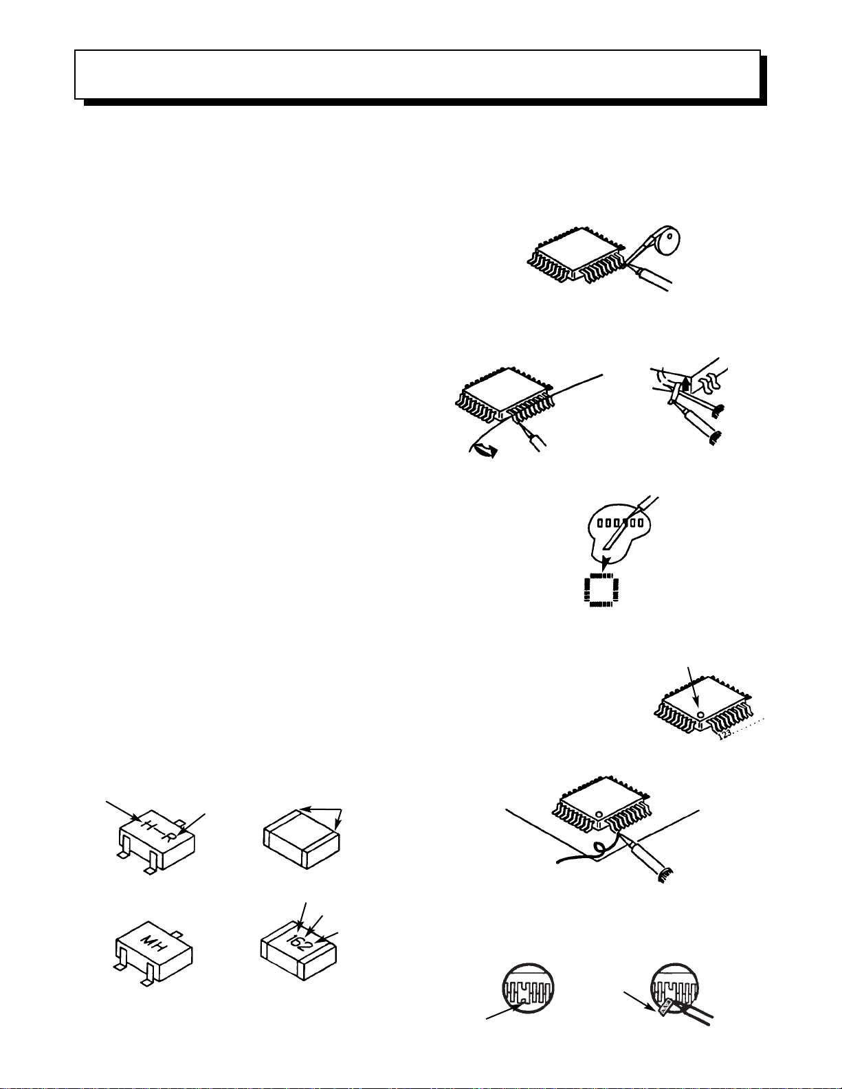
Leadless Chip Components
(surface mount)
Chip components must be replaced with identical
chips due to critical foil track spacing. There are no
holes in the board to mount standard transistors or
diodes. Some chip capacitor or resistor board solder
pads may have holes through the board, however the
hole diameter limits standard resistor replacement to
1/8 watt. Standard capacitors may also be limited for
the same reason. It is recommended that identical
chip components be used. .
Chip resistors have a three digit numerical resistance
code -1st and 2nd significant digits and a multiplier.
Example: 162 = 1600 or 1.6KΩ resistor, 0 = 0Ω
(jumper).
Chip capacitors generally do not have the value
indicated on the capacitor. The color of the component
indicates the general range of the capacitance.
Chip transistors are identified by a two letter code. The
first letter indicates the type and the second letter, the
grade of transistor.
Chip diodes have a two letter identification code as
per the code chart and are a dual diode pack with
either
common anode or common cathode. Check the parts
list for correct diode number.
Component Removal
1. Use solder wick to remove solder from component
end caps or terminals.
2. Without pulling up, carefully twist the component
with tweezers to break the adhesive.
3. Do not reuse removed leadless or chip
components since they are subject to stress
fracture during removal .
Chip Component Installation
1. Put a small amount of solder on the board
soldering pads.
2. Hold the chip component against the soldering
pads with tweezers or with a miniature alligator
clip and apply heat to the pad area with a 30 watt
iron until solder flows. Do not apply heat for more
than 3 seconds
How to Replace Flat-lC
—Required Tools—
• Soldering iron • iron wire or small awl
• De-solder braids • Magnifier
1. Remove the solder from all of the pins of a Flat-lC
by using a de-solder braid.
2. Put the iron wire under the pins of the Flat-lC and
pull it in the direction indicated while heating the
pins using a soldering iron. A small awl can be
used instead of the iron wire.
3. Remove the solder from all of the pads of the
Fiat-lC by using
a de-solder braid.
4. Position the new Flat-lC in place (apply the pins of
the Flat-lC to the soldering pads where the pins
need to be soldered). Properly
determine the positions of the
soldering pads and pins by
correctly aligning the polarity
symbol.
6. Check with a magnifier for solder bridge between
the pins or for dry joint between pins and soldering
pads. To remove a solder bridge, use a de-solder
braid as shown in the figure below.
NOTE:
These components are affixed with glue. Be careful not to break or damage any foil under the
component or at the pins of the ICs when removing. Usually applying heat to the component for a short
time while twisting with tweezers will break the component loose.
Chip Components
TYPE
GRADE
C
B
E
SOLDER
CAPS
TRANSISTOR
CAPACITOR
1ST DIGIT
2ND DIGIT
MULTIPLIER
= 1600 = 1.6K
ANODES
MH DIODE
RESISTOR
SOLDER CAPS
COMMON CATHODE
De-Solder
Braid
Soldering
Iron
Soldering
Iron
Soldering
Iron
Soldering
Iron
Soldering
Iron
Soldering
Iron
De-Solder
Braid
Flat-IC
Bridge
Solder
De-Solder
Braid
Iron
Wire
Pull
Awl
Polarity Symbol
5. Solder all pins to the soldering pads using a fine
tipped soldering iron.
Page 10
10
High Voltage limiter circuit operation check.
1. Turn off TV and connect jig as shown in Figure 2. Adjust
jig fully counter-clockwise for minimum resistance.
2. Set the AC input to 120V AC and turn on TV.
3. Confirm test pattern on CRT is a usable picture, then
slowly adjust jig until the picture disappears and TV shuts
down.
4. When the limiter circuit is operating properly, High
Voltage will be less than 31.5 kV at 1.7mAwhen TV shuts
down.
5. Turn off set immediately after checking circuit operation.
6. Unplug set for one minute to reset shutdown circuit.
Remove jig and voltmeter.
TECHNICAL CAUTIONS
(TH01)
L902
L901
C901
R901
EF901
EF901
F901
PA
1
2
KKA1
WHITE side
GND side
TESTER
AC CORD POLARITY
This check is based on the UL standard. Use the jigs specified by the production technology section. The GND side (wider
blade) of the AC power cord should be connected to K9Y1
Page 11
11
Model: 43FDX10B 53UDX10B
43FDX11B 61UDX10B
Cathode-Ray Tube:
53UDX10B/61UDX10B R=P16LFM00RFA(TU)
G=P16LFM00HHA(TU)
B=P16LFM00BMB(TU)
43FDX10B/43FDX11B R=P16LTG00RFA
G=P16LTG00HHA
B=P16LTG00BMB
Power Input: 120 volts AC, 60 Hz
Power Consumption:
¥ Stand-By Power
43FDX10B/43FDX11B . . . . . . . . . . . . .2.7W
53UDX10B/61UDX10B . . . . . . . . . . . . .2.7W
¥ Power Consumption (operating)
43FDX11B/43FDX10B . . . . . . . . . . . . .225W
53UDX10B/61UDX10B . . . . . . . . . . . .216W
¥ Power Consumption (maximum)
43FDX11B/43FDX10B . . . . . . . . . . . . .265W
53UDX10B/61UDX10B . . . . . . . . . . . .253W
Antenna Impedance: 75 Ohm Unbalanced
VHF / UHF / CATV
Receiving Channel: BAND CH
VHF 2~13
UHF 14~69
EXT. Mid (A-5)~(A-1), 4+
CATV Mid. A~I
CATV Super J~W
CATV Hyper (W+1)~(W+28)
Intermediate Frequency: Picture l-F Carrier 45.75 MHz
Sound l-F Carrier 41.25 MHz
Color Sub Carrier 42.17 MHz
Video Input: 1 Volt p-p, 75 Ohm
Video Output: 1 Volt p-p, 75 ohm
Audio Input: 470 mVrms, 47 k Ohm
Stereo Audio Output: 470 mVrms, 1 k Ohm
Audio Output Power:
Front: 12 watts per channel at 10% distortion,
8 ohm Impedance. Max output Ð 15 watts.
Anode Voltage:
30.2±0.2kv (1.32±0.2mA)
Brightness: 43 53 61
(white screen) 250cd/m
2
170cd/m
2
150cd/m
2
Speakers: 2 Woofers - 5 inch (120 mm) round
2 Tweeters - 2 inch (50 mm) round
Dimension:
43Ó 53Ó 61Ó
Height (in.) 43
5
/
8
51
5
/
8
61
1
/
8
Width (in.) 38
15
/16 46 52 3/
8
Depth (in.) 20
1
/
16
25
5
/
16
28
7
/
8
Weight (Ibs.) 148 225 283
Circuit Board Assemblies:
C.P.T. (B) P.W.B. Terminal A P.W.B.
C.P.T. (G) P.W.B. Terminal B P.W.B.
C.P.T. (R) P.W.B. VM P.W.B.
Audio Out P.W.B. Surround P.W.B.
2H P.W.B. Power Deflection P.W.B.
Power Supply P.W.B. Control P.W.B.
Signal P.W.B. Control Sub P.W.B.
Convergence P.W.B. Sensor Distribution P.W.B.
CIRCUIT PROTECTION
CAUTION: Below is an EXAMPLE only. See Replacement Parts List for details. The following symbol near the fuse
indicates fast operation fuse (to be replaced). Fuse ratings appear within the symbol.
Example:
SPECIFICATIONS
RISK OF FIRE - REPLACE FUSE AS MARKED
The rating of fuse F901 is 5A - 125V.
Replace with the same type fuse for continued protection
against fire.
F
5 A 125V
125V
5A
Page 12

12
During Insertion
1. Please refer to direction for insertion as shown in Fig. B (L position). Insert connector until “CLICK” sound is heard.
2. Make sure the connector is pressed right in, so that it has a good contact with the spring.
3. Confirm the contact by pulling the connector slightly. (Don’t pull hard because it may damage the connector).
4. Cover the high voltage output by carefully pushing silicon cover onto it. (Don’t turn the connector).
(REMARK)
1. Make sure the silicon cover is
covering the high voltage output.
CAUTIONS WHEN CONNECTING / DISCONNECTING THE HV CONNECTOR
Perform the following when the
HV connector (anode connector)
is removed or inserted for CPT
replacement, etc.
Deflection P.W.B.
Silicon cover
Wing
L Position
L Position
Wing
FBT
Anode
connector
3. Remove the connector slowly
by pulling it away from the
case.
During Removal
1. Roll out silicon cover from FBT’s contact area slowly .
2. While turning the connector about 90 degrees
following the arrow (0 position), push the connector
slightly towards the case. (Fig. A)
Fig. A
Fig. B
Silicon Cover
less than 1mm
PUSH
PUSH
Page 13
13
/
DIGITAL
ARRAY
POWER
INPUT
EXIT
SELECT
Push open door and
pull forward and down
PUSH
POWER
INPUT
EXIT
VOL+VOL-
CH-
CH+
VOL+VOL-
CH-
CH+
MENU
SELECT
MENU
Models: 43FDX11B, 43FDX10B
/
MAGIC
FOCUS
POWER
INPUT
EXIT
SELECT
Push open door and
pull forward and down
PUSH
POWER
INPUT
EXIT
VOL+VOL-
CH-
CH+
VOL+VOL-
CH-
CH+
MENU
SELECT
MENU
Models: 61UDX10B, 53UDX10B
b
c
e
P
B
P
R
f
d
AUDIO TO HI-FI
a
ANT A
TO
CONVERTER
ANT B
P
B
P
R
MONITOR
OUT
INPUT 1
AUDIO
(MONO)
L
R
AUDIO
L
R
S-VIDEOS-VIDEO
VIDEO
VIDEO
AUDIO
L
R
(MONO)
S-VIDEO
VIDEO
Y/VIDEO
R
L
AUDIO
L
R
L
R
Y/VIDEO
AUDIO
INPUT 2 INPUT 4 INPUT 5
(MONO) (MONO)
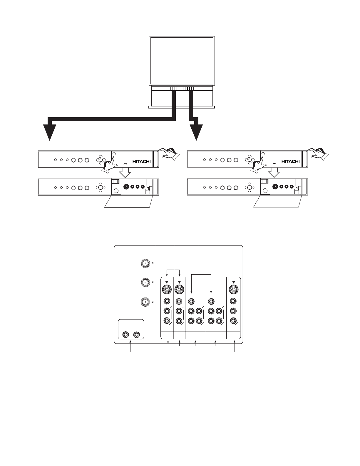
GENERAL INFORMATION
Fig. 3. Front Control Panel
Fig. 4. Rear Panel Jacks
a Antenna Input/Output
b Audio/Video Inputs 1, 2, 4, 5
c Monitor Out
d Audio to Hi-Fi
e S-Video Inputs 1 and 2
f Component Input Y-PBP
R
h
SRS
(
)
l
h
SRS
(
)
l
Page 14
14
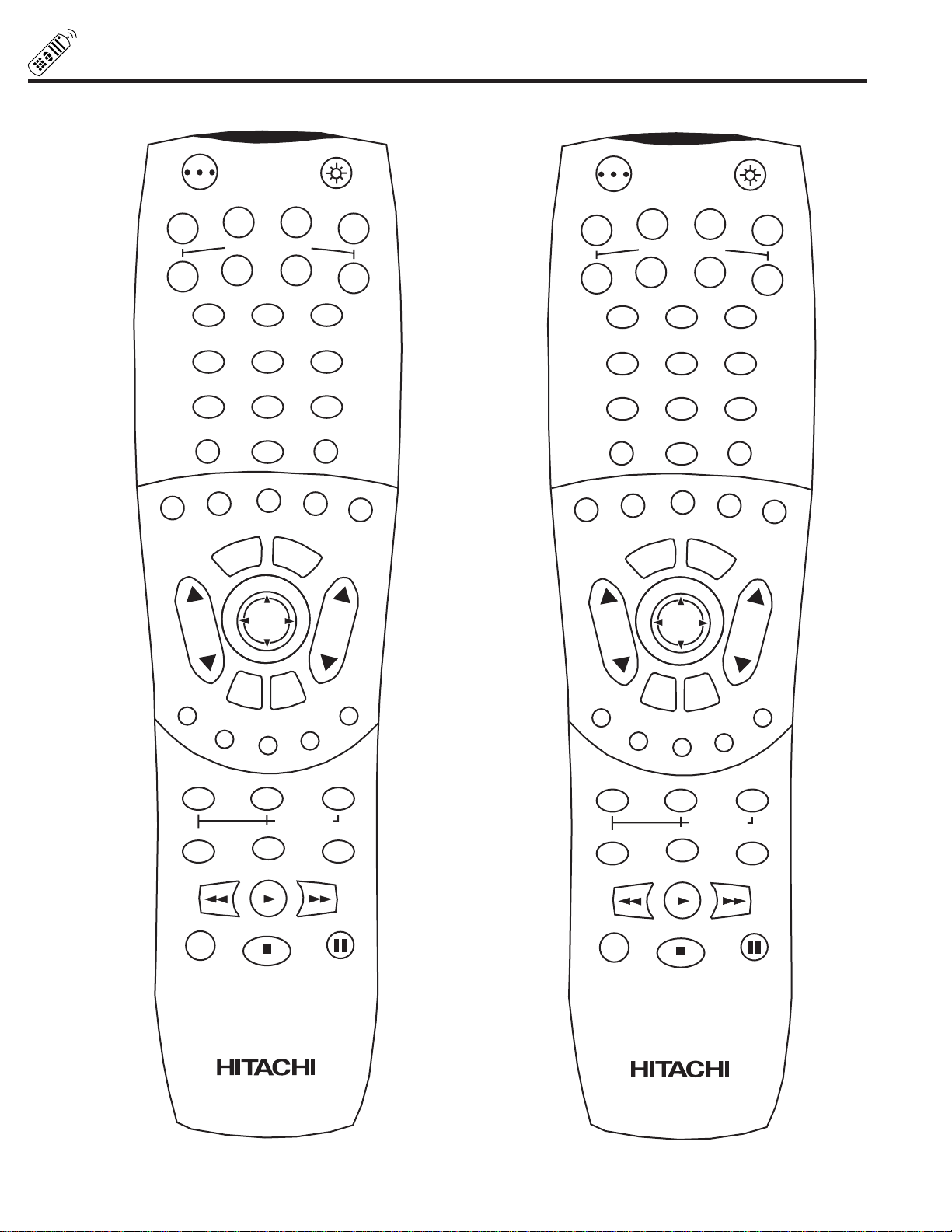
USE THE REMOTE TO CONTROL YOUR TV
POWER
TV
VCR
CBL
AV2
AV1
AV3
STB
DVD
1
2
4
56
3
7
89
0
LAST CHSLEEP
ANT
HELP
PIX
EXIT
MENU
CHVOL
STATUS
MUTE
GUIDE/TVGUIDE/TVGUIDE/TV
INFO
VCR PLUS+
SVCS
GUIDE/TV
SCHD
PIP PIP CH
SWAP
FREEZE
PIP MODE
PIP ACCESS
PROG
TV/VCR
SLOW
SOURCE WIZARD
REC
SELECT
C.C.
ASPECT
VID 1
VID 2
VID 3
VID 4
VID 5
CLU-5711TSI
CLU-5711TSI
POWER
TV
VCR
CBL
TAPE
CD
AMP
STB
DVD
1
2
4
56
3
7
89
0
LAST CHSLEEP
ANT
HELP
MODE
EXIT
MENU
CHVOL
STATUS
MUTE
GUIDE/TVGUIDE/TVGUIDE/TV
INFO
VCR PLUS+
SVCS
GUIDE/TV
SCHD
PIP PIP CH
SWAP
FREEZE
PIP MODE
PIP ACCESS
PROG
TV/VCR
SLOW
SOURCE WIZARD
REC
SELECT
C.C.
ASPECT
VID 1
VID 2
VID 3
VID 4
VID 5
CLU-5713TSI
CLU-5713TSI
Page 15
15
Press the front panel
MAGIC FOCUS
button momentarily
for auto setup.
VIDEO
Select VIDEO to adjust picture settings and improve picture quality.
Use this function to change the contrast between black and white levels in the picture. This adjustment
will only affect the picture when ADVANCED SETTINGS PERFECT PICTURE is OFF.
Use the THUMB STICK G or H to highlight the function to be adjusted.
Press the THUMB STICK F or E to adjust the function.
Press EXIT to quit menu.
NOTE: 1. It may be necessary to adjust TINT to obtain optimum picture quality when using the COMPONENT:
Y-PBPRInput jacks.
2. If you are using the COMPONENT VIDEO input jacks (Y-P
BPR
) and notice that the TINT and COLOR are
abnormal, check to make sure that COMPONENT SET-COLOR SYSTEM is set properly.
Use this function to adjust flesh tones so they appear natural. (See notes below.)
Use this function to adjust overall picture brightness.
Use this function to adjust the amount of fine detail in the picture.
When RESET is selected, press down on THUMB STICK E to return video adjustments to factory
preset conditions.
CONTRAST
Use this function to adjust the level of color in the picture.
COLOR
TINT
BRIGHTNESS
SHARPNESS
RESET
Menu To Menu Bar To Quit Exit
Menu To Menu Bar To Quit Exit
100%
50%
50%
50%
MENU
THUMB
STICK
THUMB
STICK
100%
CUSTOMIZE
SETUP
VIDEO
AUDIO
THEATER
SEL
Contrast
Contrast
Brightness
Color
Tint
Sharpness
Reset
Advanced
Settings
CUSTOMIZED PICTURE AND SOUND ADJUSTMENTS
MAGIC
FOCUS
MAGIC FOCUS
MAGIC FOCUS
The Magic Focus button on the front panel will align the convergence when pressed.
Page 16
16
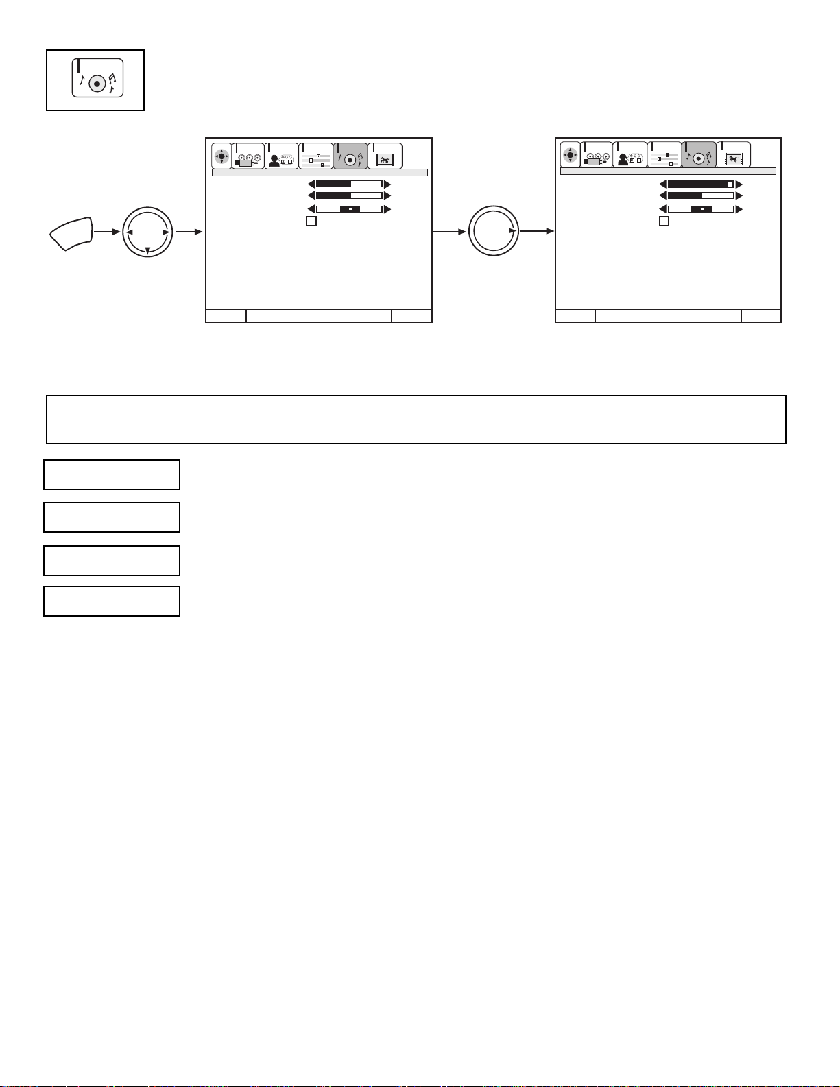
Select AUDIO to adjust the TV to your preference and to improve the sound quality.
AUDIO
ExitExit
90%
50%
Bass
Treble
Balance
Reset
Advanced
Settings
50%
50%
THUMB
STICK
THUMB
STICK
MENU
CUSTOMIZE
SETUP
VIDEO
AUDIO
THEATER
SEL
CUSTOMIZE
SETUP
VIDEO
AUDIO
THEATER
SEL
Menu To Menu Bar To QuitMenu To Menu Bar To Quit
Bass
Treble
Balance
Reset
Advanced
Settings
This function controls the low frequency audio to all speakers.
Use THUMB STICK G or H to highlight the function to be adjusted.
Press THUMB STICK F or E to adjust the function.
Press EXIT to quit MENU.
NOTE: If BASS is selected you are adjusting BASS. The additional menu items TREBLE and BALANCE can be selected and
adjusted in the same manner.
This function controls the high frequency audio to all speakers.
This function will control the left to right balance of the TV internal speakers and the AUDIO TO HI FI output.
When RESET is selected, press CURSOR E to return audio adjustments to factory preset conditions.
BASS
BALANCE
RESET
TREBLE
Page 17
17
P
B
P
R
AUDIO TO HI-FI
P
B
P
R
MONITOR
OUT
INPUT 1
AUDIO
(MONO)
L
R
AUDIO
L
R
S-VIDEOS-VIDEO
VIDEO
VIDEO
AUDIO
L
R
(MONO)
S-VIDEO
VIDEO
Y/VIDEO
R
L
AUDIO
L
R
L
R
Y/VIDEO
AUDIO
INPUT 2 INPUT 4 INPUT 5
(MONO) (MONO)
ANT A
TO
CONVERTER
ANT B
DVD Player
Stereo System Amplifier
Laserdisc player, VCR,
camcorder, etc.
VCR #2
Cable TV Box
VCR #1
Outside antenna or
cable TV coaxial cable
2-Way signal splitter
OUTPUT
Y P
B
P
R
L R
HDTV Set-Top Box
V L R
OUTPUT
S-VIDEO
ANT
IN
OUTPUT
S-VIDEO
VL R
OUTPUT
YP
B/CBPR/CR
L R
LR
INPUT
V L R
INPUT
S-VIDEO
INPUT
OUTPUT
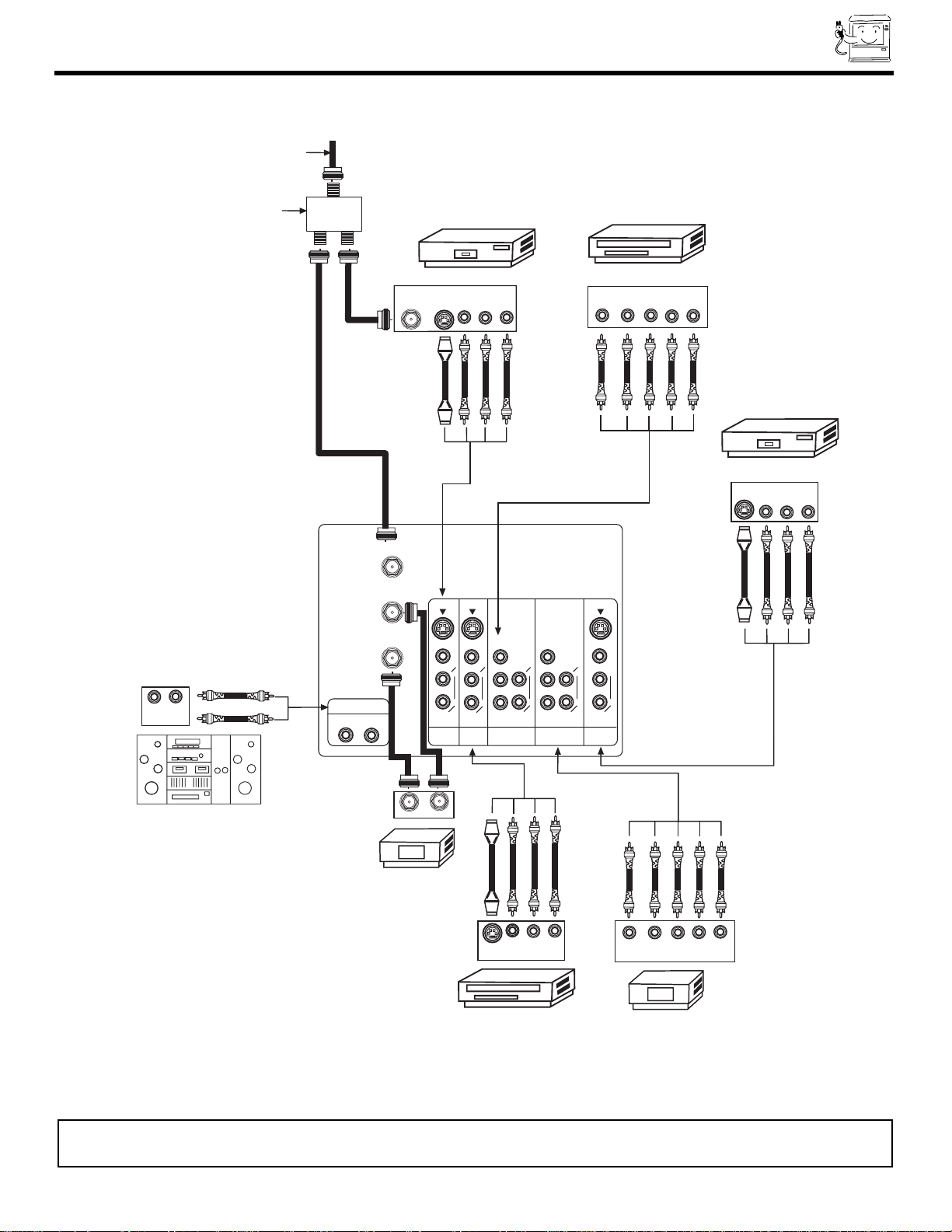
REAR PANEL CONNECTIONS
NOTE: 1.
Connect only 1 component to each input jack.
2. Follow connections that pertain to your personal entertainment system.
TYPICAL FULL-FEATURE SETUP
Page 18
18
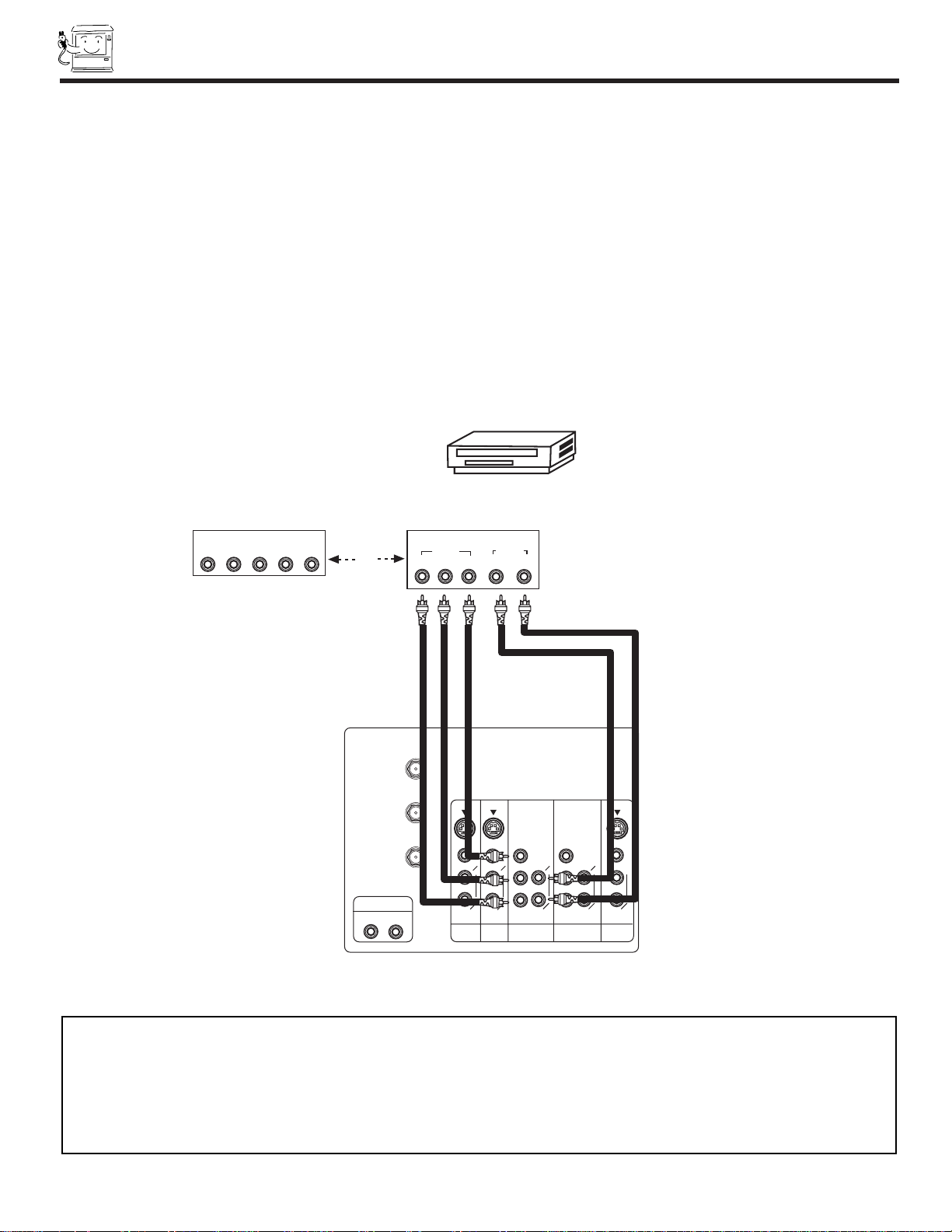
CONNECTING EXTERNAL VIDEO SOURCES
CONNECTING A COMPONENT SOURCE TO VIDEO 4 OR 5: Y-PBPR.
1. Connect the cable from the Y OUT of the Laserdisc/DVD player or HDTV set top box to the INPUT (Y) jack, as shown on the TV
set below.
2. Connect the cable from the CB/PBOUT or B-Y OUT of the Laserdisc/DVD player or HDTV set top box to the INPUT (PB)jack.
3. Connect the cable from the CR/PROUT or R-Y OUT of the Laserdisc/DVD player or HDTV set top box to the INPUT (PR) jack.
4. Connect the cable from the AUDIO OUT R of the Laserdisc/DVD player or HDTV set top box to the INPUT (AUDIO/R) jack.
5. Connect the cable from the AUDIO OUT L of the Laserdisc/DVD player or HDTV set top box to the INPUT (AUDIO/L) jack.
6. Press the VID4~VID5 button, to view the program from the Laserdisc/DVD player or HDTV set top box. The VIDEO icon
disappears automatically after approximately eight seconds.
7. Press the ANT button to return to the previous channel.
P
B
P
R
AUDIO TO HI-FI
P
B
P
R
MONITOR
OUT
INPUT 1
AUDIO
(MONO)
L
R
AUDIO
L
R
S-VIDEOS-VIDEO
VIDEO
VIDEO
AUDIO
L
R
(MONO)
S-VIDEO
VIDEO
Y/VIDEO
R
L
AUDIO
L
R
L
R
Y/VIDEO
AUDIO
INPUT 2 INPUT 4 INPUT 5
(MONO) (MONO)
ANT A
TO
CONVERTER
ANT B
Rear Panel of Television
OUTPUT
P
R/CR PB/CB
Y
L R
AUDIO
VIDEO
DVD Player
OR
Hitachi Model or
Similar Model
Back of
DVD Player
OUTPUT
L R Y P
B
P
R
HDTV Set-Top Box
NOTE: 1. You may use standard video signal for INPUT:4 and 5.
2. Completely insert the connection cord plugs when connecting to rear panel jacks. The picture and sound that is
played back will be abnormal if the connection is loose.
3. See page 17 for tips on REAR PANEL CONNECTIONS.
Page 19
19
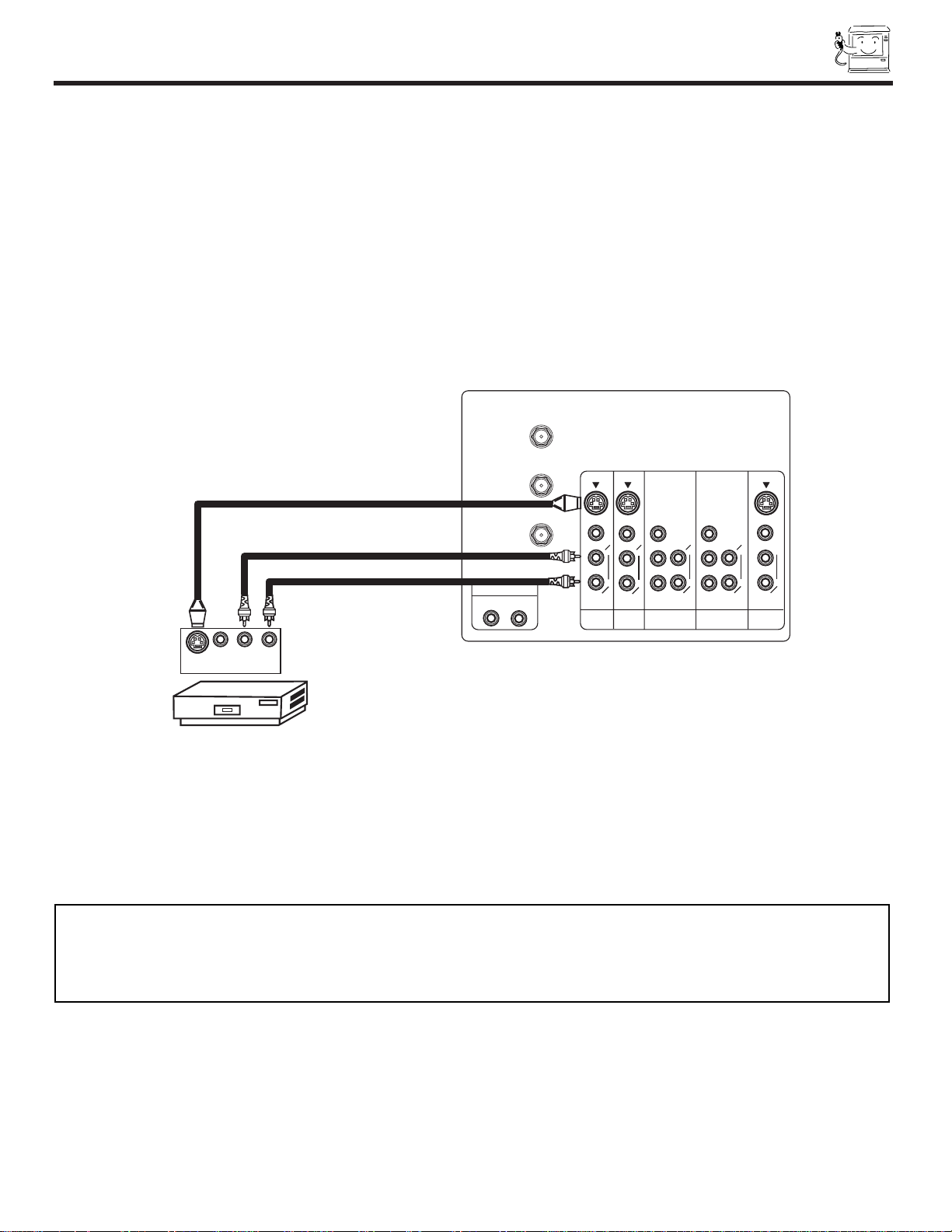
CONNECTING EXTERNAL VIDEO SOURCES
CONNECTING AN S-VIDEO SOURCE TO INPUT 1, 2 AND 3
1. Connect the cable from the S-VIDEO OUT of the VCR or the laserdisc player to the INPUT (S-VIDEO) jack, as shown on the TV
set below.
2. Connect the cable from the AUDIO OUT R of the VCR or the laserdisc player to the INPUT (AUDIO/R) jack.
3. Connect the cable from the AUDIO OUT L of the VCR or the laserdisc player to the INPUT (AUDIO/L) jack.
4. Press the VID1~VID3 button to view the program from the VCR or laserdisc player. The VIDEO icon disappears automatically
after approximately eight seconds.
5. Press the ANT button to return to the previous channel.
P
B
P
R
AUDIO TO HI-FI
P
B
P
R
MONITOR
OUT
INPUT 1
AUDIO
(MONO)
L
R
AUDIO
L
R
S-VIDEOS-VIDEO
VIDEO
VIDEO
AUDIO
L
R
(MONO)
S-VIDEO
VIDEO
Y/VIDEO
R
L
AUDIO
L
R
L
R
Y/VIDEO
AUDIO
INPUT 2 INPUT 4 INPUT 5
(MONO) (MONO)
ANT A
TO
CONVERTER
ANT B
Hitachi Model or
Similar Model
Rear Panel of Television
VCR or Laserdisc Player
V L R
OUTPUT
S-VIDEO
NOTES: 1. Completely insert the connection cord plugs when connecting to rear panel jacks. The picture and sound that is
played back will be abnormal if the connection is loose.
2. A single VCR can be used for VCR #1 and VCR #2, but note that a VCR cannot record its own video or line
output. Refer to your VCR operating guide for more information on line input-output connections.
Back of
VCR
Page 20
20
CONNECTING EXTERNAL VIDEO SOURCES
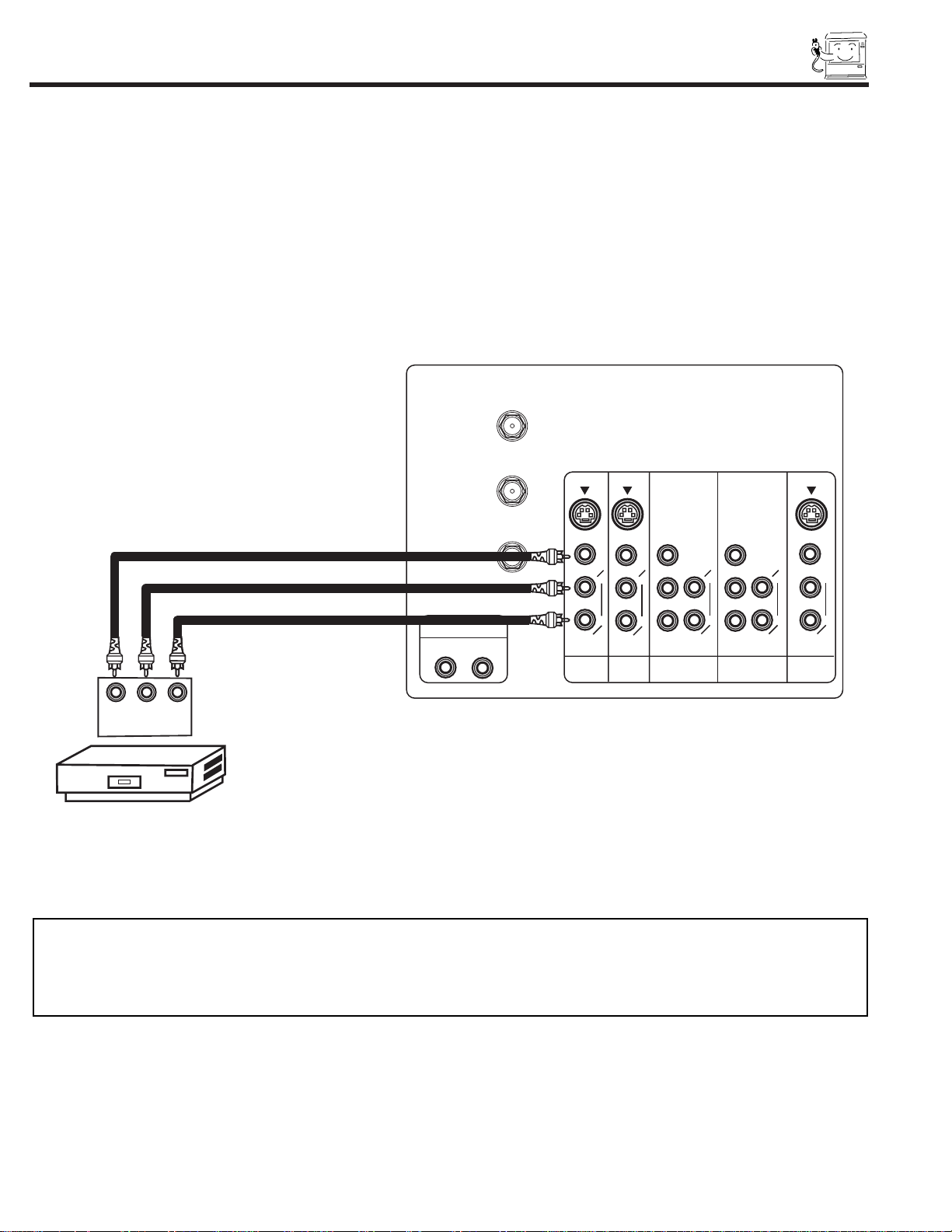
CONNECTING A STEREO SOURCE TO INPUT1~INPUT5
1. Connect the cable from the VIDEO OUT of the VCR or the laserdisc player to the INPUT (VIDEO) jack, as shown on the TV set
below.
2. Connect the cable from the AUDIO OUT R of the VCR or the laserdisc player to the INPUT (AUDIO/R) jack.
3. Connect the cable from the AUDIO OUT L of the VCR or the laserdisc player to the INPUT (AUDIO/L) jack.
4. Press the VID1~VID5 button to view the program from the VCR or laserdisc player. The VIDEO icon disappears automatically
after approximately eight seconds.
5. Press the VID1~VID5 button to return to the previous channel.
P
B
P
R
AUDIO TO HI-FI
P
B
P
R
MONITOR
OUT
INPUT 1
AUDIO
(MONO)
L
R
AUDIO
L
R
S-VIDEOS-VIDEO
VIDEO
VIDEO
AUDIO
L
R
(MONO)
S-VIDEO
VIDEO
Y/VIDEO
R
L
AUDIO
L
R
L
R
Y/VIDEO
AUDIO
INPUT 2 INPUT 4 INPUT 5
(MONO) (MONO)
ANT A
TO
CONVERTER
ANT B
Hitachi Model or
Similar Model
Back of
VCR
V L R
VCR
OUTPUT
NOTES: 1. Completely insert the connection cord plugs when connecting to rear panel jacks. The picture and sound that is
played back will be abnormal if the connection is loose.
2. A single VCR can be used for VCR #1 and VCR #2, but note that a VCR cannot record its own video or line
output. Refer to your VCR operating guide for more information on line input-output connections.
Page 21

21
FEATURE INFORMATION
As the digital era dawns, Hitachi has models that provide the best possible images today...and tomorrow. Our HDTV Ready
model incorporates new Flex Converter technology to display a high quality 720P (high definition scanning) or 480P
(progressive scanning) image; this same circuitry enables it to accept a full 1080i HDTV signal from a digital set-top box now
or in the future.
FLEX CONVERTER TECHNOLOGY
With current analog broadcasts, there is just one level of picture quality. In the new age of digital TV, there will be several levels.
The highest, called HDTV, can be as high as 1080i.The next level, called HDTV, can be 720P. The standard level, SDTV, can
be 480P or 480i. Hitachi has developed the Flex Converter, advanced circuitry that allows your UltraVision FDX and UDX series
television to produce true 1080i HDTV resolution with an HDTV set-top box. It converts analog 480i signals to the higherquality 540P signals with no scan lines or flicker. The FDX and UDX needs a set-top box to receive any Digital Signal.
COMPONENT VIDEO
Component Video inputs accept separate blue, red & B/W signals from a high resolution digital source as DVD or digital settop box to provide a higher resolution picture.
3DYC (DIGITAL 3DYC COMB FILTER)
The Digital 3DYC Comb Filter analyzes three lines of information from a single video frame as well as lines from adjacent
frames. This technology eliminates the flickering that a detailed pattern or scene would normally cause, for the cleanest,
neatest picture possible.
PROGRESSIVE SCANNING
A standard TV uses Interlaced Scanning where each frame of video is broken into two fields, each providing alternating scan
lines. This can leave noticeable scan lines and cause flickering. With Progressive Scanning, complete frames are displayed for
a smoother picture with no scan lines and no flicker. This allows you to get the optimal picture quality from todayÕs high
resolution digital sources such as DVD or a digital set-top box.
Page 22
22
SET UP
SETUP
The PICTURE FORMATS function is very useful when setting up reception High Definition, Standard
Definition and NTSC signals.
V. Position
Adjust this when viewing a COMPONENT: Y-PBPRsignal. This feature is used to center an HDTV video signal between the top and
bottom gray bars. Adjustable range is -10 (video center is toward bottom of screen) to +10 (video center is toward top of screen).
Press THUMB STICK G or H to highlight then press down on THUMB STICK to select.
Press EXIT to quit menu or THUMB STICK F to return to previous menu.
PICTURE FORMATS
Picture Formats Ant A 6
Aspect Style Aspect 1
Aspect 2
Aspect 3
Aspect 4
Aspect 5
V. Position +5
Comp Color Type HDTV
SDTV/DVD
Video Display 1080i
540P
Menu To Menu Bar To Quit Exit
THUMB
STICK
THUMB
STICK
Menu To Menu Bar To Quit Exit
Menu To Menu Bar To Quit Exit
THUMB
STICK
Press Select To Set
Press Select To Set
SETUP
SEL
SETUP
SEL
CUSTOMIZE
SETUP
VIDEO
AUDIO
THEATER
SEL
Picture Formats Ant A 6
Aspect Style Aspect 1
Aspect 2
Aspect 3
Aspect 4
Aspect 5
V. Position +5
Comp Color Type HDTV
SDTV/DVD
Video Display 1080i
540P
Set Menu Language
Plug & Play
Set Antenna/Cable
Set Channel Memory
Edit Channel Memory
View Channel List
Set The Clock
Magic Focus
Picture Formats
SELECT
NOTE: 1. Depending on the input signal, some of the Aspect features will be grayed out. This means that the feature is
not available with the signal input.
2. Set up a Component Signal (connect component to Y-PBPRinputs) and switch to VIDEO: 4 or 5 by pressing the
Video:4 or 5 button on the Remote Control when planning to use all Picture Formats feature.
Aspect 1 - Display the actual (normal 4x3 or 16x9) inputted signal mode.
Aspect 2 - Stretch the signal to 16x9 format.
Aspect 3 - Zoom in on Aspect 1 mode.
Aspect 4 - Zoom in on Aspect 2 mode.
Aspect 5 - When 1080i signal is inputted, this is the true 1080i signal.
Page 23
23
SET UP
SETUP
4x3
480i
Aspect 1
540p/1080i
Aspect
key
Aspect
key
Input
Aspect 1
(4x3 mode)
Aspect 2
(16x9 mode)
Aspect
key
Aspect
key
Aspect 4
(Zoom 2 mode)
Aspect 3
(Zoom 1 Mode)
Aspect 3
540p/1080i
Aspect 4
540p/1080i
Normal
Aspect
key
Aspect
key
Aspect 2
405p/810i
Letter
16x9
480i
Input
Aspect
key
Aspect
key
Aspect 1
(4x3 mode)
Aspect 2
(16x9 mode)
Aspect
key
Aspect
key
Aspect 4
(Zoom 2 mode)
Aspect 3
(Zoom 1 Mode)
Aspect 3
540p/1080i
Aspect 4
540p/1080i
Normal
Aspect
key
Aspect
key
Aspect 2
405p/810i
Aspect 1
540p/1080i
4x3
NTSC
Aspect 1
540p/1080i
Aspect 3
540p/1080i
Aspect
key
Aspect
key
Input
Aspect 1
(4x3 mode)
Aspect 3
(Zoom 1 Mode)
Letter
16x9
NTSC
Aspect
key
Aspect
key
Input
Aspect 1
(4x3 mode)
Aspect 3
(Zoom 1 Mode)
Aspect 3
540p/1080i
Aspect 1
540p/1080i
Normal
Press Select To Set
SETUP
SEL
Picture Formats Y-PBPR: 4
Aspect Style Aspect 1
Aspect 2
Aspect 3
Aspect 4
Aspect 5
V. Position +5
Comp Color Type HDTV
SDTV/DVD
Video Display 1080i
540P
Menu To Menu Bar To Quit Exit
Input
Signal
Press Select To Set
SETUP
SEL
Picture Formats Y-PBPR: 4
Aspect Style Aspect 1
Aspect 2
Aspect 3
Aspect 4
Aspect 5
V. Position +5
Comp Color Type HDTV
SDTV/DVD
Video Display 1080i
540P
Menu To Menu Bar To Quit Exit
Press Select To Set
SETUP
SEL
Picture Formats Y-PBPR: 4
Aspect Style Aspect 1
Aspect 2
Aspect 3
Aspect 4
Aspect 5
V. Position +5
Comp Color Type HDTV
SDTV/DVD
Video Display 1080i
540P
Menu To Menu Bar To Quit Exit
Press Select To Set
SETUP
SEL
Picture Formats Y-PBPR: 4
Aspect Style Aspect 1
Aspect 2
Aspect 3
Aspect 4
Aspect 5
V. Position +5
Comp Color Type HDTV
SDTV/DVD
Video Display 1080i
540P
Menu To Menu Bar To Quit Exit
Press Select To Set
SETUP
SEL
Picture Formats Y-PBPR: 4
Aspect Style Aspect 1
Aspect 2
Aspect 3
Aspect 4
Aspect 5
V. Position +5
Comp Color Type HDTV
SDTV/DVD
Video Display 1080i
540P
Menu To Menu Bar To Quit Exit
Press Select To Set
SETUP
SEL
Picture Formats Y-PBPR: 4
Aspect Style Aspect 1
Aspect 2
Aspect 3
Aspect 4
Aspect 5
V. Position +5
Comp Color Type HDTV
SDTV/DVD
Video Display 1080i
540P
Menu To Menu Bar To Quit Exit
Normal
(1) NTSC Input - ANT A/B, VID1 ~ VID5, - 4x3 Format
(2) 480i Input - ANT A/B, Input 4/5 (Component) - 4x3 Format
Picture Formats
Depending on the input signal, the PICTURE FORMAT aspect ratio allows you to adjust the image through the following options.
Page 24
24
SET UP
SETUP
4x3
480p
Aspect 1
540p/1080i
Aspect
key
Aspect
key
Input
Aspect 1
(4x3 mode)
Aspect 2
(16x9 mode)
Aspect
key
Aspect
key
Aspect 4
(Zoom 2 mode)
Aspect 3
(Zoom 1 Mode)
Aspect 3
540p/1080i
Aspect 4
540p/1080i
Normal
Aspect
key
Aspect
key
Aspect 2
405p/810i
Letter
16x9
480p
Input
Aspect
key
Aspect
key
Aspect 1
(4x3 mode)
Aspect 2
(16x9 mode)
Aspect
key
Aspect
key
Aspect 4
(Zoom 2 mode)
Aspect 3
(Zoom 1 Mode)
Aspect 3
540p/1080i
Aspect 4
540p/1080i
Normal
Aspect
key
Aspect
key
Aspect 2
405p/810i
Aspect 1
640p/1080i
Press Select To Set
SETUP
SEL
Picture Formats Y-PBPR: 4
Aspect Style Aspect 1
Aspect 2
Aspect 3
Aspect 4
Aspect 5
V. Position +5
Comp Color Type HDTV
SDTV/DVD
Video Display 1080i
540P
Menu To Menu Bar To Quit Exit
Press Select To Set
SETUP
SEL
Picture Formats Y-PBPR: 4
Aspect Style
Aspect 1
Aspect 2
Aspect 3
Aspect 4
Aspect 5
V. Position +5
Comp Color Type HDTV
SDTV/DVD
Video Display 1080i
540P
Menu To Menu Bar To Quit Exit
Press Select To Set
SETUP
SEL
Picture Formats Y-PBPR: 4
Aspect Style
Aspect 1
Aspect 2
Aspect 3
Aspect 4
Aspect 5
V. Position +5
Comp Color Type HDTV
SDTV/DVD
Video Display 1080i
540P
Menu To Menu Bar To Quit Exit
Press Select To Set
SETUP
SEL
Picture Formats Y-PBPR: 4
Aspect Style Aspect 1
Aspect 2
Aspect 3
Aspect 4
Aspect 5
V. Position +5
Comp Color Type HDTV
SDTV/DVD
Video Display 1080i
540P
Menu To Menu Bar To Quit Exit
Comp Color Type
The Comp Color Type function allows you to automatically change tint and color coordinate for DTV Programs.
HDTV - High Definition Television - Use for High Vision Signal Y-PBPRfrom HDTV Set-Top Box.
SDTV /DVD - Standard Definition Television or Digital Video Disc Y-CBCRsuch as DVD (Digital Video Disc Player).
Video Display
The video display feature allows you to select between 1080i or 540P signal display.
NOTE: 1. If Comp Color Type is set improperly (does not match actual input signal), the color and tint of the main picture will be
abnormal.
2. You must be tuned to VIDEO: 4 or 5 input and have a component hooked up to the Y-PBPRinput jacks to
access all Picture Formats menu.
3. All settings will affect only the component input you are currently viewing. If you are using both sets of component
input jacks, be sure to set the Picture Formats feature for both inputs (set VIDEO:4 AND
VIDEO:5).
(3) 480p Input - Input 4/5 (Component) - 4x3 Format
Page 25
25
4x3
NTSC
Input
Aspect 1
540p/1080i
Aspect 3
540p/1080i
540 Lines (Progressive)
1080 Lines (Interlaced)
540 Lines (Progressive)
1080 Lines (Interlaced)
4x3
480i
Aspect 1
540p/1080i
Input
Aspect 3
540p/1080i
Aspect 4
540p/1080i
Aspect 2
405p/810i
540 Lines (Progressive)
1080 Lines (Interlaced)
405 Lines
(Progressive)
810 Lines
(Interlaced)
540 Lines (Progressive)
1080 Lines (Interlaced)
540 Lines (Progressive)
1080 Lines (Interlaced)
540 Lines
(Progressive)
1080 Lines
(Interlaced)
Insertion Panel to top and bottom
DISPLAY FORMAT OF COMPONENT VIDEO TERMINAL (YCBCR/YPBPR).
SDTV SIGNAL FORMAT: SMPTE-170M
HDTV SIGNAL FORMAT: ITU-R709, SMPTE-274M
4X3 MODEL
1. NORMAL MODE
(1) NTSC: 480i 4x3 (15.75kHz) 540P/1080i (33.75kHz)
(2) SDTV: 480i 4x3 (15.75kHz) 540P/1080i (33.75kHz)
Page 26
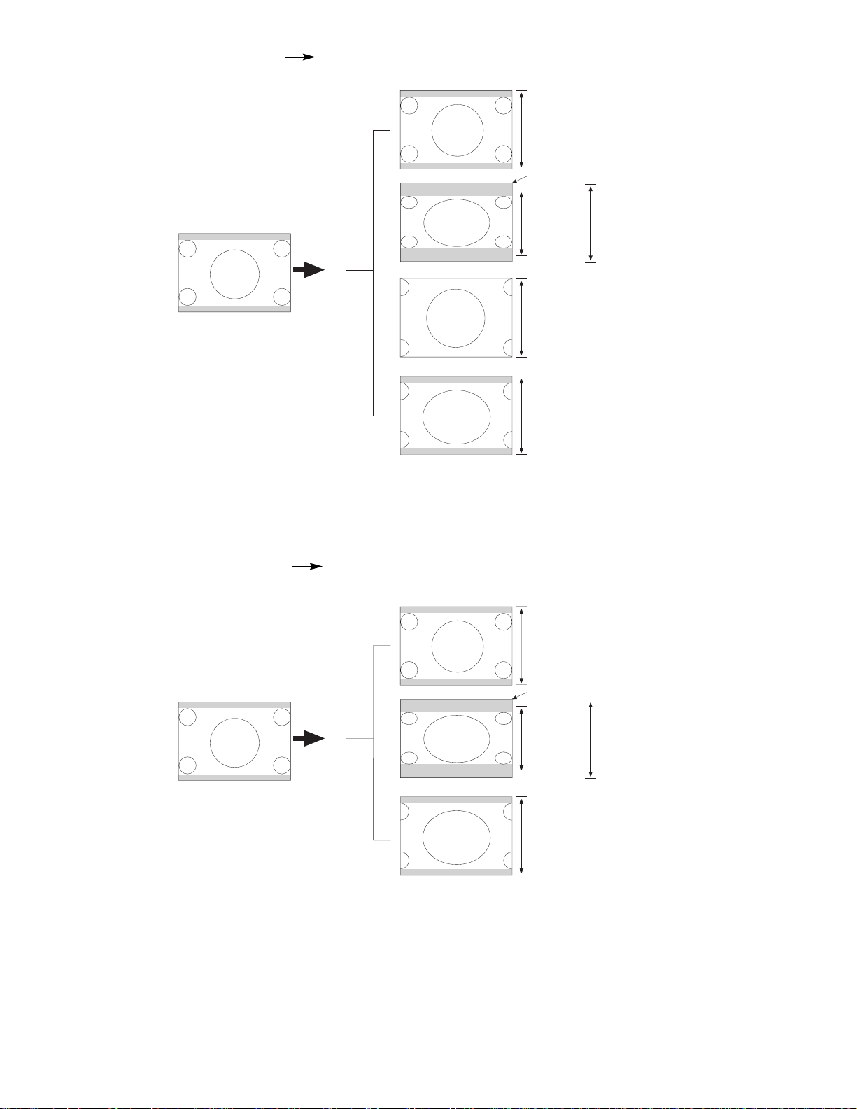
26
(3) SDTV: 480i 16X9 (15.75KHz) 540P/1080i (33.75KHz)
540 Lines (Progressive)
1080 Lines (Interlaced)
405 Lines
(Progressive)
810 Lines
(Interlaced)
540 Lines (Progressive)
1080 Lines (Interlaced)
540 Lines (Progressive)
1080 Lines (Interlaced)
540 Lines
(Progressive)
1080 Lines
(Interlaced)
Insertion Panel to top and bottom
Letter
16x9
480i
Input
Aspect 3
540p/1080i
Aspect 4
540p/1080i
Aspect 2
405p/810i
Aspect 1
540p/1080i
540 Lines (Progressive)
1080 Lines (Interlaced)
405 Lines
(Progressive)
810 Lines
(Interlaced)
540 Lines (Progressive)
1080 Lines (Interlaced)
Hor 3/4 V
Ver 3/4 V
540 Lines (Progressive)
1080 Lines (Interlaced)
Hor 3/4 V
540 Lines
(Progressive)
1080 Lines
(Interlaced)
Insertion Panel to top and bottom
4x3
480p
Aspect 1
540p/1080i
Input
Aspect 3
540p/1080i
Aspect 4
540p/1080i
Aspect 2
405p/810i
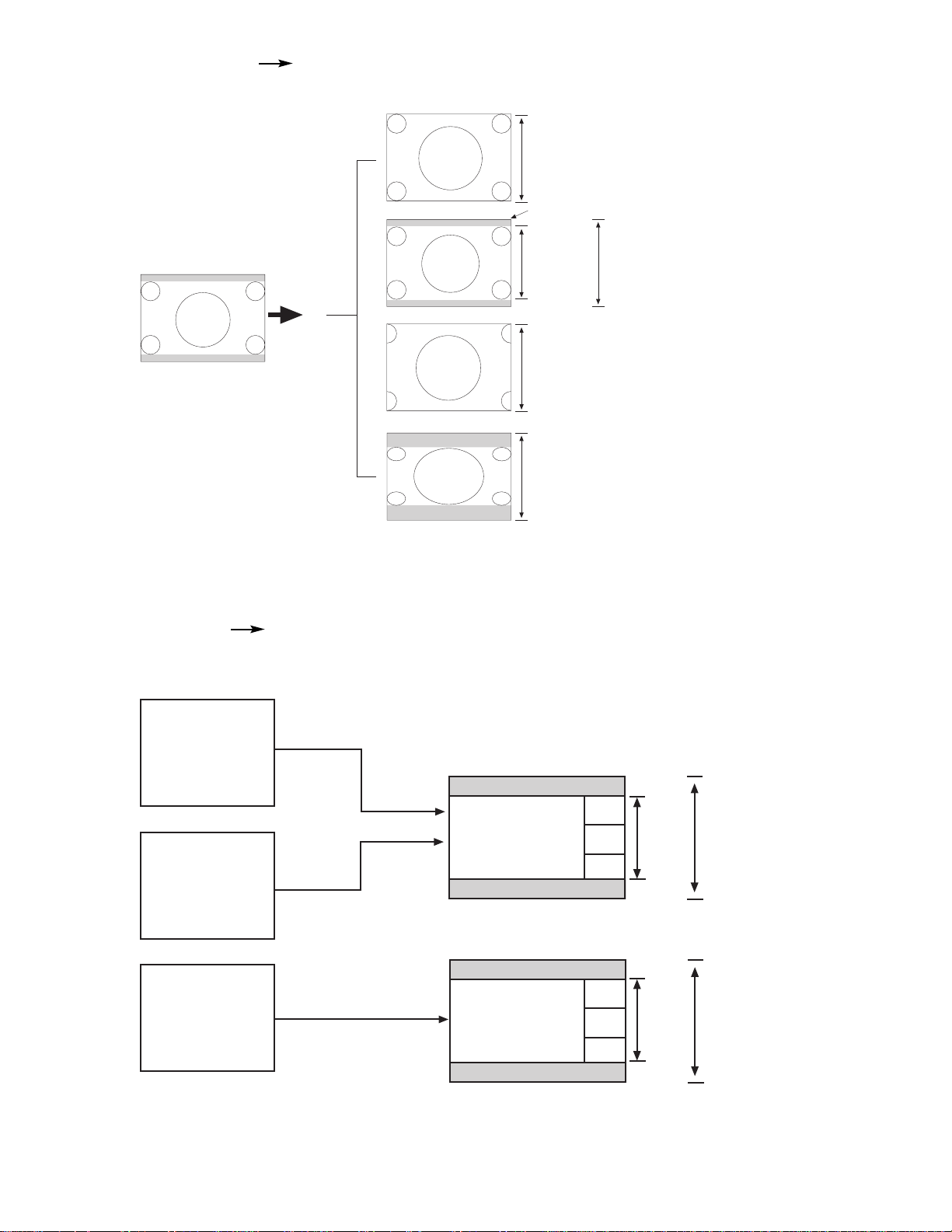
(4) SDTV: 480P 4x3 (31.5KHz) 540P/1080i (33.75KHz)
Page 27
27
(5) SDTV: 480P 16X9 (31.5KHz) 540P/1080i (33.75KHz)
540 Lines (Progressive)
1080 Lines (Interlaced)
405 Lines
(Progressive)
810 Lines
(Interlaced)
540 Lines (Progressive)
1080 Lines (Interlaced)
Hor 3/4 V
Ver 3/4 V
540 Lines (Progressive)
1080 Lines (Interlaced)
Hor 3/4 V
540 Lines
(Progressive)
1080 Lines
(Interlaced)
Insertion Panel to top and bottom
Letter
16x9
480p
Input
Aspect 3
540p/1080i
Aspect 4
540p/1080i
Aspect 2
405p/810i
Aspect 1
640p/1080i
540 Lines (Progressive)
1080 Lines (Interlaced)
405 Lines
(Progressive)
810 Lines
(Interlaced)
540 Lines (Progressive)
1080 Lines (Interlaced)
540 Lines
(Progressive)
1080 Lines
(Interlaced)
Insertion Panel to top and bottom
Letter
16x9
720p
Input
Aspect 4
540p/1080i
Aspect 2
405p/810i
Aspect 1
540p/1080i
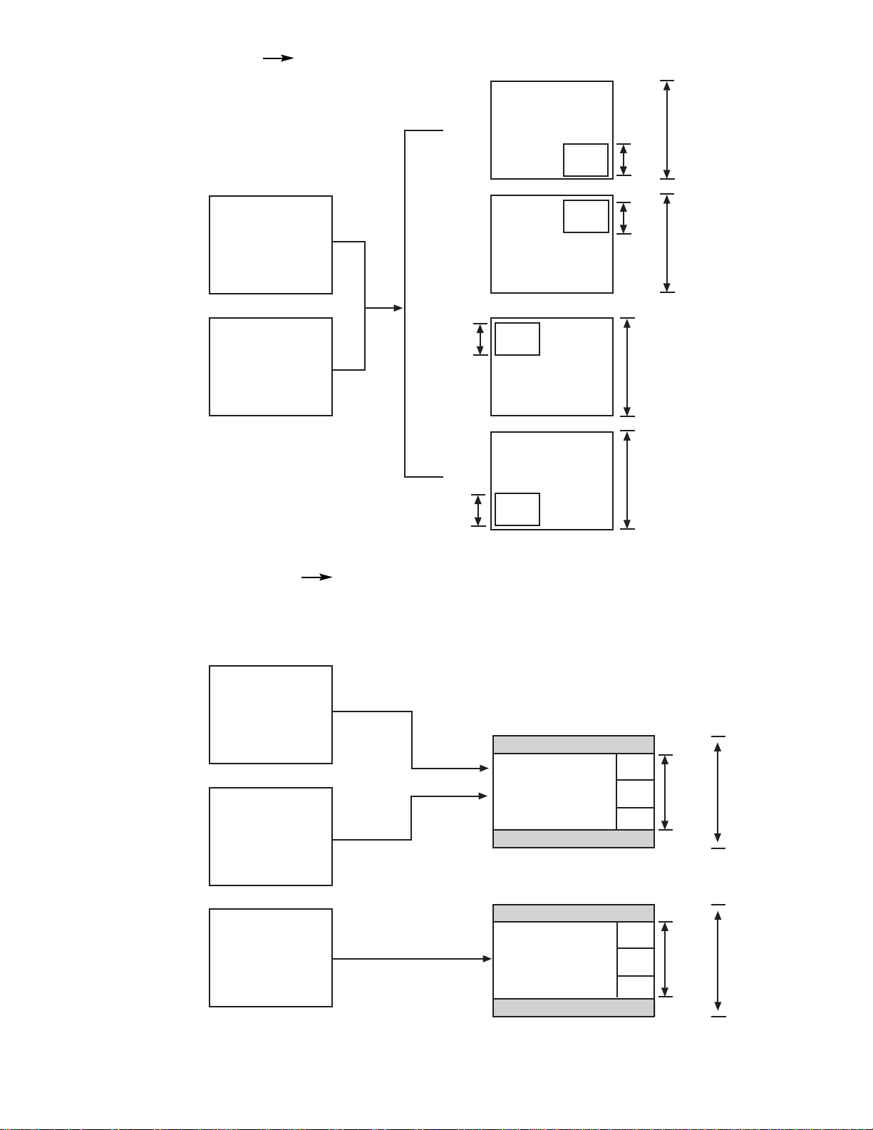
(6) HDTV: 720P 16x9 (33.75KHz) 540P/1080i (33.75KHz)
Page 28
28
(7) HDTV: 1080i 16X9 (33.75KHz) 1080i 4x3 (33.75KHz)
1080 Lines (Interlaced)
810 Lines
(Interlaced)
1080 Lines (Interlaced)
Hor 3/4 V
1080 Lines (Interlaced)
1080 Lines
(Interlaced)
Insertion Panel to top and bottom
16x9
1080i
Input
Aspect 4
1080i
Aspect 2
405p/810i
Aspect 2
810i
Aspect 1
1080i
Main
Picture
405
Lines
SUB
SUB
SUB
Main
Picture
Sub
Picture
NTSC
Picture
405
Lines
Moving
Picture
540
Lines
540
Lines
STROBE
STROBE
STROBE
(8) Surf/Strobe Mode NTSC 540P 4x3 (33.75KHz)
Page 29
29
Main Picture
NTSC/480i
Sub Picture
NTSC/480i
Main
Picture
Main
Picture
Main
Picture
Main
Picture
Sub
Sub
Sub
Sub
540
Lines
169
Lines
169
Lines
540
Lines
169
Lines
169
Lines
540
Lines
540
Lines
Main
Picture
405
Lines
SUB
SUB
SUB
Main
Picture
ANT A
Sub
Picture
ANT A
NTSC/480i
Picture
405
Lines
Moving
Picture
STROBE
540
Lines
540
Lines
STROBE
STROBE
(10) Surf/Strobe Mode NTSC/480i 540P 4x3 (33.75KHz)
(9) Single Mode NTSC/480i 540P 4x3 (33.75KHz)
Page 30

30
SERVICE ADJUSTMENTS
1. ASSEMBLED P.W.B ADJUSTMENT..................................................................................................................31
1-1. Service Menu Access (NTSC, SDTV and HDTV) ..................................................................................31
1-2. Comb Filter Operation Check ................................................................................................................39
1-3. Audio Operation Check ..........................................................................................................................39
1-3-1. Tone Control Operation Check ....................................................................................................39
1-3-2. Perfect Volume Operation Check ................................................................................................39
1-3-3. SRS Surround Operation Check ..................................................................................................39
1-3-4. BBE Surround Operation Check ..................................................................................................39
1-4. High Voltage Adjustment ........................................................................................................................40
2. FINAL ASSEMBLY ADJUSTMENT (Adjustment should be according to below order)..............................40
2-1. Cut Off Adjustment..................................................................................................................................40
2-2. DCU Phase Data Setting (Normal and 1080i Throught mode) ..............................................................40
2-3. Horizontal Position Adjustment (Coarse) ................................................................................................41
2-4. Raster Tilt (Deflection Yoke)....................................................................................................................41
2-5. Beam Alignment......................................................................................................................................41
2-6. Raster Position........................................................................................................................................42
2-7. Vertical Size (Normal Mode Only) ..........................................................................................................42
2-8. Horizontal Size (Normal Mode Only) ......................................................................................................42
2-9. Beam Form ............................................................................................................................................43
2-10. Lens Focus..............................................................................................................................................43
2-11. Static Focus ............................................................................................................................................45
2-12. Digital Convergence (Normal and 1080i Throught mode) ......................................................................45
2-12-1. Magic Focus Character Set Up ..................................................................................................46
2-12-2. Magic Focus Pattern Set Up ......................................................................................................47
2-12-3. Convergence Jig Screen Specification ......................................................................................48
2-12-4. Raster Position Adjsutment ........................................................................................................49
2-12-5. Convergence Point Adjustment ..................................................................................................49
2-13. Blue Defocus ..........................................................................................................................................51
2-14. White Balance ........................................................................................................................................51
2-15. Sub Brightness........................................................................................................................................52
2-16. Sub-Picture Siganl Amplitude Adjustment ..............................................................................................54
2-17. Horizontal Position (Normal and 1080i Throught mode) ........................................................................55
2-18. Scanning Area Check (Normal and 1080i Throught mode)....................................................................55
2-19. Raster Distortion Check (Normal and 1080i Throught mode) ................................................................56
3. ADJUSTMENT POINT ........................................................................................................................................58
3-1. CRT (R)(G)(B), Cabinet Locations..........................................................................................................58
3-2. Main Chassis (Signal P.W.B.) ................................................................................................................59
3-3. Main Chassis (Power/Deflection P.W.B.) ................................................................................................60
3-4. Power Supply P.W.B. ..............................................................................................................................62
3-5. CPT (R)(G)(B), Focus Pack, Control P.W.B. ..........................................................................................63
*IMPORTANT
For many of the above adjustments, it is necessary to have an HDTV (1080i or 720P) signal generator, SDTV
(480P) signal generator, as well as the usual NTSC (480i) signal generator.
Hitachi recognizes that few companies offer HDTV or SDTV signal generators and that the cost of these
generators is sometimes prohibitive. For this reason, we suggest the use of a set-top-box for HDTV and SDTV
adjustments. Usually, there is a switch on the set-top-box which enables it to output HDTV (1080i or 720P) or
SDTV (480P) signals even with no input. In this case, the sync is automatically detected by the TV (at the Y-P
BPR
Inputs on the rear panel).
Page 31

31
1. ASSEMBLED P.W.B. ADJUSTMENT
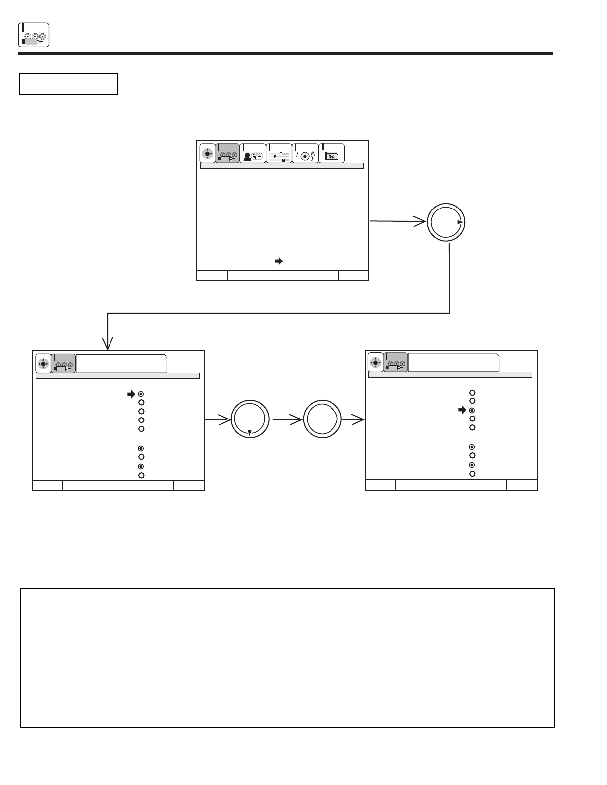
1.1 Service Menu Access
Adjustment Procedure
(1) To access Service Menu press and hold INPUT key on Control Panel and then press POWER key on control
panel to access I2C adjustment mode.
(2) Receive signal on main picture. (NTSC, SDTV or HDTV).
Some menu pages have I2C adjustments for SDTV and HDTV. The set will automatically allow you to set
these items only when a SDTV or HDTV signal is input to the COMPONENT jacks on the back of the TV.
See table below.
(3) Check the OSD according to table on pages 32~38, using THUMB STICK G, H on Remote Control.
*: Adjustable Data
Others: Fixed Data (be careful not to change)
(4) Press EXIT key to exit I2C ADJUST mode.
NOTE: (1) If the TV I2C data is different from the I2C Parameter (pages 32~38) for fixed data, change the data
to match pages 32~38.
(2) When exchanging microprocessor or EEPROM and TV is turned on for first time, it requires
initialization of Memory Initial of I2C adjustment menu.
Page 32

32
1.2 I
2
C Parameter List
(1) Adjust Mode OSD
Press INPUT + POWER
of control panel.
B CUT 3F
G CUT 3F
R CUT 3F
G DRV 3F
ADJUST MODE XXXXXXXX
SERVICE
SUB BRT*
WHITE BAL
R DRV (COOL)* 3F
B DRV (COOL)* 3F
R CUTOFF (COOL)* 80
G CUTOFF (COOL)* 80
B CUTOFF (COOL) 80
H POSITION* 3F
V POSITION* 3F
FACT RESET
CH U/D, INPUT
ADJUST MODE
SERVICE
SUB BRT
WHITE BAL
R DRV (COOL) 48
B DRV (COOL) 37
R CUTOFF (COOL) 80
G CUTOFF (COOL) 80
B CUTOFF (COOL) 80
H POSITION 12
V POSITION 00
FACT RESET
CH U/D, INPUT
Select SERVICE
and press E key
Press EXIT key
(OSD OFF)
CUT OFF ADJUST MODE
ADJUST MODE
SERVICE
SUB BRT
WHITE BAL
R DRV (COOL) 3F
B DRV (COOL) 3F
R CUTOFF (COOL) 80
G CUTOFF (COOL) 80
B CUTOFF (COOL) 80
H POSITION 3F
V POSITION 3F
FACT RESET
CH U/D, INPUT
MENU
Select SERVICE
and press E key
Press EXIT key
R DRV 3F
MENU
MENU
Select SUB BRT
and press E key
Press EXIT key
BRIGHTNESS 80
Press F E to adjust
VIDEO SETTINGS
(1) CONTRAST : MIN
(2) COLOR : MIN
VIDEO SETTINGS
(1) CONTRAST : MAX
(2 ) COLOR,TINT,SHARP,BRIGHT:CENER
(3) COLOR TEMP : COOL
ADJUST
(1) Press G H to select the G DRV.,
R DRV., R CUT, G CUT, B CUT.
(Initial position G/B DRV). G/B
DRV, B/R DRV select by the DR R
and DR BG.
(2) Press F E to adjust.
WHITE BALANCE
ADJ. MODE
INPUT + POWER
Only adjust
in cool mode.
Only adjust
in cool mode.
Only adjust
in cool mode.
*: Adjustable data
others: Fixed data (be careful not to change)
A
SUB BRIGHT
ADJ. MODE
G H
(DEFAULT)
Page 33

33
ADJUST MODE
SERVICE
SUB BRT*
WHITE BAL*
G DRV (COOL)* 3F
R DRV (COOL)* 3F
R CUTOFF (COOL)* 80
G CUTOFF (COOL)* 80
B CUTOFF (COOL) 80
H POSI (V/P)* 3F
47 VD-POS (FC)* 3F
FACT RESET
CH U/D, INPUT
CH U/D, INPUT
CH U/D, INPUT CH U/D, INPUT
CH U/D, INPUT
SELECT
SELECT
CH U/D, INPUT
WARM, NTSC, STD ADJ MODE
1. Press G H to select the G DRV or R DRV.
2. Press select to change the COOLRWARMR
NTSCRCOOL mode. Adjust on each mode,
but cannot adjust on the COOL mode.
3. WARM and NTSC mode data is offset data
based on the COOL mode data.
4. Do not adjust WHITE BALANCE in WARM or
NTSC mode. Adjust in COOL mode only.
CH U/D, INPUT
SELECT
MENU GH
SELECT
ADJUST MODE
SERVICE
SUB BRT*
WHITE BAL*
G DRV (COOL)* 48
R DRV (COOL)* 4F
R CUTOFF (COOL)* 80
G CUTOFF (COOL)* 80
B CUTOFF (COOL) 80
H POSI (V/P)* 3F
47 VD-POS (FC)* 3F
FACT RESET
ADJUST MODE
SERVICE
SUB BRT*
WHITE BAL*
G DRV (COOL)* 4E
R DRV (COOL)* 58
R CUTOFF (COOL)* 80
G CUTOFF (COOL)* 80
B CUTOFF (COOL) 80
H POSI (V/P)* 3F
47 VD-POS (FC)* 3F
FACT RESET
ADJUST MODE
SERVICE
SUB BRT*
WHITE BAL*
G DRV (COOL)* 3F
R DRV (COOL)* 3F
R CUTOFF (COOL)* 80
G CUTOFF (COOL)* 80
B CUTOFF (COOL) 80
H POSI H* 3F
47 VD-POS (FC)H* 3F
FACT RESET
ADJUST MODE
SERVICE
SUB BRT*
WHITE BAL*
G DRV (COOL)* 3F
R DRV (COOL)* 3F
R CUTOFF (COOL)* 80
G CUTOFF (COOL)* 80
B CUTOFF (COOL) 80
H POSI* 3F
47 VD-POS (FC)* 3F
FACT RESET
Other Mode 1080i through mode
Other Mode 1080i through mode
SELECT
Only adjust
in cool mode.
VD Position Adj Mode
Press F E to adjust
H Position Adj Mode
Press F E to adjust
1.2 I
2
C Parameter List Cont.
Page 34

34
ADJUST MODE
YUVSEL RESET
3DYC RESET
1HV/C RESET
FLEX RESET
2HV/P RESET
BBE RESET
MEMORY INIT
I2COPEN
CH U/D, INPUT
Same data of
Main and Sub
ADJUST MODE
TA1270-M
TINT (TV) 3C
TOFF0 (TV) 00
TOFQ (TV) 00
SUB CNT* 0F
SUB CLR 0F
CH U/D, INPUT
}
}
Press G H to select.
Press E to set to the
initial data of each
device.
Press G H to select.
Press E for complete
memory re-initialization
MENU
G H
Item Device
YUVSEL CXA2141Q
3DYC uPD64082
1HV/C TA1270BF
FLEX FLEX CONT.
2HV/P TA1316AN
BBE NJW1132
ADJUST MODE
TA1270-S
TINT (TV) 3C
TOFF0 (TV) 00
TOFQ (TV) 00
SUB CNT* 0F
SUB CLR 0F
SPLIT/SINGLE
MODE
+
PiP CH
SURF
mode
(ANT A only)
SPLIT
mode
SINGLE
mode
(NTSC only)
NORMAL
mode
PIP
ON/OFF
key
PIP
Mode
key
PIP
Mode
key
PIP Mode key
ADJUST MODE
CXA2151
MAT OUT 0
H WIDTH 0
V TC 1
HSEP 0
HS MASK 1
CH U/D, INPUT
ADJUST MODE
CXA2151
MACRO 1
GAIN SEL 0
CBGAIN 7
CRGAIN 7
YGAIN 7
CH U/D, INPUT
MENU GH
MENU GH
ADJUST MODE
UPD64082
DYGA 09
DCGA 06
VAPGA 00
VAPIN 0B
YHCOR 00
CH U/D, INPUT
MENU GH
MENU GH
MENU GH
Not used
1.2 I
2
C Parameter List Cont.
NOTE: Memory Init. will reset all devices and factory settings. Use factory reset from previous page to restore unit to factory settings condition.
Page 35

35
SELECT
MENU G H
FLEX CONT 480i
39 HHPF1 00
41 V-CRG 00
42 H-CRG 00
43 V-ENH 02
44 H-ENH 00
96 YVHENH 0B
100 CVHENH 12
71 YV-ENH 00
87 YH-ENH 07
480i mode
FLEX CONT 480P
39 HHPF1 00
41 V-CRG 00
42 H-CRG 00
43 V-ENH 02
44 H-ENH 00
96 YVHENH 0B
100 CVHENH 12
71 YV-ENH 00
87 YH-ENH 07
480P mode
FLEX CONT 1080i
39 HHPF1 00
41 V-CRG 00
42 H-CRG 00
43 V-ENH 00
44 H-ENH 00
96 YVHENH 00
100 CVHENH 12
71 YV-ENH 00
87 YH-ENH 00
1080i mode
FLEX CONT 720P
39 HHPF1 00
41 V-CRG 00
42 H-CRG 00
43 V-ENH 02
44 H-ENH 00
96 YVHENH 0B
100 CVHENH 12
71 YV-ENH 00
87 YH-ENH 07
720P mode
FLEX CONT SPLIT
39 HHPF1 00
41 V-CRG 00
42 H-CRG 00
43 V-ENH 02
44 H-ENH 00
96 YVHENH 0B
100 CVHENH 12
71 YV-ENH 00
87 YH-ENH 07
SPLIT mode
CH U/D, INPUT
FLEX CONT NTSC
39 HHPF1 00
41 V-CRG 00
42 H-CRG 00
43 V-ENH 02
44 H-ENH 00
96 YVHENH 0B
100 CVHENH 12
71 YV-ENH 00
87 YH-ENH 07
NTSC/SINGLE/SURF/STROBE mode
SELECT SELECT SELECT SELECT
SELECT
FLEX CONT 480i
94 CH-ENH 0F
68 YV-CLP 00
84 YH-CLP 00
97 YV-NLP 00
98 YH-NLP 0A
83 YH-FRQ 00
91 CH-FRQ 02
70 YV-LT1 00
480i mode
FLEX CONT 480P
94 CH-ENH 0F
68 YV-CLP 00
84 YH-CLP 00
97 YV-NLP 00
98 YH-NLP 0A
83 YH-FRQ 00
91 CH-FRQ 02
70 YV-LT1 00
480P mode
FLEX CONT 1080i
94 CH-ENH 0F
68 YV-CLP 00
84 YH-CLP 00
97 YV-NLP 00
98 YH-NLP 00
83 YH-FRQ 00
91 CH-FRQ 02
70 YV-LT1 00
1080i mode
FLEX CONT 720P
94 CH-ENH 0F
68 YV-CLP 00
84 YH-CLP 00
97 YV-NLP 00
98 YH-NLP 0A
83 YH-FRQ 00
91 CH-FRQ 02
70 YV-LT1 00
720P mode
FLEX CONT SPLIT
94 CH-ENH 0F
68 YV-CLP 00
84 YH-CLP 00
97 YV-NLP 00
98 YH-NLP 0A
83 YH-FRQ 00
91 CH-FRQ 02
70 YV-LT1 00
SPLIT mode
CH U/D, INPUT
FLEX CONT NTSC
94 CH-ENH 0F
68 YV-CLP 00
84 YH-CLP 00
97 YV-NLP 00
98 YH-NLP 0A
83 YH-FRQ 00
91 CH-FRQ 02
70 YV-LTI 00
NTSC/SINGLE/SURF/STROBE mode
SELECT SELECT SELECT SELECT
MENU G H
MENU G H
MENU G H MENU G H MENU G H
SELECT
SELECT
MENU G H
MENU G H
1.2 I
2
C Parameter List Cont.
Page 36

36
SELECT
MENU G H
FLEX CONT 480i
86 YH-LTI 01
93 CH-CTI 01
95 Y-CRG 00
64 YNR-IN 04
73 CNR-IN 04
80 YNRPAS 00
88 CNRPAS 02
40 READ-F 0F
55 LINE-I 00
480i mode
FLEX CONT 480P
86 YH-LTI 01
93 CH-CTI 01
95 Y-CRG 00
64 YNR-IN 04
73 CNR-IN 04
80 YNRPAS 00
88 CNRPAS 02
40 READ-F 0F
55 LINE-I 00
480P mode
FLEX CONT 1080i
86 YH-LTI 00
93 CH-CTI 01
95 Y-CRG 00
64 YNR-IN 04
73 CNR-IN 04
80 YNRPAS 00
88 CNRPAS 02
40 READ-F 0F
55 LINE-I 00
1080i mode
FLEX CONT 720P
86 YH-LTI 01
93 CH-CTI 01
95 Y-CRG 00
64 YNR-IN 04
73 CNR-IN 04
80 YNRPAS 00
88 CNRPAS 02
40 READ-F 0F
55 LINE-I 00
720P mode
FLEX CONT SPLIT
86 YH-LTI 01
93 CH-CTI 01
95 Y-CRG 00
64 YNR-IN 04
73 CNR-IN 04
80 YNRPAS 00
88 CNRPAS 02
40 READ-F - -
55 LINE-I 00
SPLIT mode
CH U/D, INPUT
FLEX CONT NTSC
86 YH-LTI 01
93 CH-CTI 01
95 Y-CRG 00
64 YNR-IN 04
73 CNR-IN 04
80 YNRPAS 00
88 CNRPAS 02
40 READ-F 0F
55 LINE-I 00
NTSC/SINGLE/SURF/STROBE mode
SELECT SELECT SELECT SELECT
SELECT
FLEX CONT 480i
65 YNRRDC 01
74 CNRRDC 00
89 CNR-0 00
27 FRMBRT 60
11 MVW-PH 07
18 SVW-PH 07
14 MHS-HP 0F
21 SHS-HP 0F
23 V-POS 1F
50 HD-POS 3F
480i mode
FLEX CONT 480P
65 YNRRDC 01
74 CNRRDC 00
89 CNR-0 00
27 FRMBRT 60
11 MVW-PH 05
18 SVW-PH 05
14 MHS-HP 0F
21 SHS-HP 0F
23 V-POS 1F
50 HD-POS 3F
480P mode
FLEX CONT 1080i
65 YNRRDC 00
74 CNRRDC 00
89 CNR-0 00
27 FRMBRT 60
11 MVW-PH 04
18 SVW-PH 04
14 MHS-HP 0F
21 SHS-HP 0F
23 V-POS 1F
50 HD-POS 3F
1080i mode
FLEX CONT 720P
65 YNRRDC 00
74 CNRRDC 00
89 CNR-0 00
27 FRMBRT 60
11 MVW-PH 06
18 SVW-PH 06
14 MHS-HP 0F
21 SHS-HP 0F
23 V-POS 1F
50 HD-POS 3F
720P mode
FLEX CONT SPLIT
65 YNRRDC 01
74 CNRRDC 00
89 CNR-0 00
27 FRMBRT 60
11 MVW-PH - -
18 SVW-PH - -
14 MHS-HP - -
21 SHS-HP - -
23 V-POS 1F
50 HD-POS 3F
SPLIT mode
CH U/D, INPUT
FLEX CONT NTSC
65 YNRRDC 01
74 CNRRDC 00
89 CNR-0 00
27 FRMBRT 60
11 MVW-PH 07
18 SVW-PH 07
14 MHS-HP 0F
21 SHS-HP 0F
23 V-POS 1F
50 HD-POS 3F
NTSC/SINGLE/SURF/STROBE mode
SELECT SELECT SELECT SELECT
MENU G H
MENU G H
MENU G H MENU G H MENU G H
SELECT
SELECT
MENU G H
MENU G H
FLEX CONT
48 VBLK-T 7F
49 VBLK-B 7F
51 HBLK-R 88
52 HBLK-L 7A
35 FRMTOP 07
36 FRMBTM 07
37 FRMRGT 07
38 FRMLFT 07
CH U/D, INPUT
SELECT
FLEX CONT 1080i PASS
48 VBLK-T 7F
49 VBLK-B 7F
51 HBLK-R 7F
52 HBLK-L 7F
35 FRMTOP 07
36 FRMBTM 07
37 FRMRGT 07
38 FRMLFT 07
1080i pass
MENU G H
FLEX CONT
120 TV/CINE 01
121 T/C DET 07
122 T/C UNL 01
123 T/C LCK 03
126 T/C ARE 05
127 T/C CBR 07
128 T/C YBR 07
129 IPMODE 00
130 C-INT 00
CH U/D, INPUT
MENU G H
MENU G H
1.2 I
2
C Parameter List Cont.
Page 37

37
SELECT
MENU G H
FLEX CONT 480i/480P
SHARP 28
APACON 01
CLT 01
SRT GA 00
SRT FQ 03
480i/480P mode
FLEX CONT 720P/1080i
SHARP 1C
APACON 00
CLT 01
SRT GA 00
SRT FQ 03
720P/1080i mode
FLEX CONT 1080i PASS
SHARP 1C
APACON 00
CLT 01
SRT GA 00
SRT FQ 03
1080i pass mode
FLEX CONT SPLIT
SHARP 28
APACON 01
CLT 01
SRT GA 00
SRT FQ 03
SPLIT mode
CH U/D, INPUT
FLEX CONT NTSC
SHARP 30
APACON 01
CLT 01
SRT GA 00
SRT FQ 03
NTSC/SINGLE/SURF/STROBE mode
SELECT SELECT SELECT SELECT
SELECT
TA1316 SDTV
COLOR 54
TINT 3D
R-Y PH 02
R/B GA 0D
G-Y PH 05
G/B GA 00
SDTV mode
TA1316 HDTV
COLOR 4F
TINT 41
R-Y PH 00
R/B GA 0A
G-Y PH 05
G/B GA 00
HDTV mode
CH U/D, INPUT
TA1316 NTSC
COLOR 54
TINT 3B
R-Y PH 02
R/B GA 0C
G-Y PH 02
G/B GA 00
NTSC mode
SELECT
MENU G H
SELECT
SELECT
MENU G H
MENU G H
}
Center Adjust
1.2 I
2
C Parameter List Cont.
Page 38

38
MENU
G H
TA1316
RGB ACL 01
RGB BRT 3F
RGB CNT 7F
OSD ACL 00
OSD BRT 02
OSD CNT 03
R REF 01
G/B REF 01
SUB CNT 15
TA1316
DCRR SW 00
COLORG 00
YC GA1 00
YC GA2 00
VSM PH 03
VSM GA 07
TA1316
YOUTG 00
WPL AP 00
Y DTL 10
WP PNT 07
WP GA 00
HI BRT 00
WPS 01
CDE 00
TA1316
WPL LE 00
WPL F0 07
DABL PN 00
DABL GA 07
ABL PN 07
ABL GA 05
DYNC PNT 00
DYNC GA 00
STAT GA 00
CH U/D, INPUT
TA1316
CLP PHS 00
SCP SW 01
HBP PHS 00
VBLK PHS 1F
PRES PH1 0F
PRES PH2 00
MENU
G H
MENU
G H
MENU
G H
MENU
G H
NJW1132
BBE HIGH 07
BBE LOW 07
V CHIP RATING
POLLING 0F
TIMEOUT 05
STATUS 02
AFC/CLOCK TEST
OSD POSITION
H POSI OE
V POSI 00
CH U/D, INPUT
TA1316
DC PNT 00
DC RAT 00
DC LMT 00
BSP 04
APL/BS 00
BLC 00
BDL 00
BS ARE 01
S TRK 00
Select OSD
POSI and
press E key
MENU G H
MENU G H
}
Press EXIT key
TEST
CXA2151 (MAIN)
H**
V**
Input4 00
Input5 00
MENU
G H
}
32ms*POLLING DATA
FROM RATING OFF
DETECTIVE COUNT
CXA2151 READ MODE
H COUNT DATA
V COUNT DATA
MENU
G H
SELF-DIAGNOSIS
RESET START 00
REMOTE POWER 00
MATRIX POWER 00
REMOTE MEM INIT 00
MATRIX MEM INIT 00
ADJUST MEM INIT 00
ADJUST FAC RESET 00
EEP READ ERROR 00
EEP WRITE ERROR 00
LAST EVENT 0000
CCD SLICE 13
CCD LPF 03
MENU G H
A
1.2 I
2
C Parameter List Cont.
Page 39

39
1.2 Comb filter operation check
Adjustment preparation
(1) Receive the color bar signal at the regular tuning
point.
(2) Set the CONTRAST control to MAX and the other
controls to center.
(3) Set the PERFECT PICTURE to OFF.
Adjustment procedure
(1) Check that between the color bars there are line dots
every second color bar as shown in the drawing.
A
A A
B
LINE DOT
AX
BX
Check and line dots.
B
A
1.3 AUDIO OPERATION CHECK
1.3.1 TONE CONTROL OPERATION CHECK
Adjustment preparation
(1) Input an audio signal of 250Hz and 3KHz in order
with level of 150mVrms to the L/mono audio input.
(2) Set the Volume to around the center.
(3) Set SRS SURROUND to OFF.
(4) Set LOUDNESS to OFF.
(5) Set INTERNAL SPEAKER to ON.
Adjustment procedure
(1) Select BASS mode and check that the audio output
level of the speakers changes to emphasized or
suppressed when adjusted to max. or min. of the
adjustment mode.
(2) Select TREBLE mode and check that the audio
ouput level of the speakers changes by emphasized
or suppressed when adjust to max. or min. of the
adjustment mode.
(3) Select BALANCE mode and check that the audio
output changes right or left when adjusted to right or
left of the adjustment mode.
1.3.2 PERFECT VOL. OPERATION CHECK
Adjustment preparation
(1) Set PERFECT VOL. mode to on.
(2) Set the Volume to around the center.
(3) Set to SURROUND OFF.
(4) Set INTERNAL SPEAKER to ON.
Adjustment procedure
(1) Input 100mVrms, 200mVrms, 300mVrms and
400mVrms of 1KHz audio signal to L/Mono terminal.
(2) Check that same level sound is ouput from SP when
200mVrms, 300mVrms and 400mVrms of 1KHz
sound signal is input.
1.3.3 SRS SURROUND OPERATION CHECK
Adjustment preparation
(1) Set the Master Volume to around the center. (Vol.30)
(2) Set the BALANCE to the center.
(3) Set the BASS and TREBLE to the center.
(4) Set LOUDNESS to OFF.
(5) Set PERFECT VOLUME to OFF.
(6) Set INTERNAL SP to ON.
(7) Set BBE to OFF.
(8) Input the audio signal of 400Hz in order with level of
1Vpp to the R audio input and no signal to the L
audio input.
Adjustment procedure
Check the following waveform at the HiFi out.
Output SRS
ON OFF
HiFi L out 0.35±0.05Vpp No signal
HiFi R out 1.0±0.05Vpp 0.2±0.05Vpp
1.3.4 BBE SURROUND OPERATION CHECK
Adjustment preparation
(1) Set the Master Volume to around the center. (Vol.30)
(2) Set the BALANCE to the center.
(3) Set the BASS and TREBLE to the center.
(4) Set LOUDNESS to OFF.
(5) Set PERFECT VOLUME to OFF.
(6) Set INTERNAL SP to ON.
(7) Set SRS to OFF.
(8) Input the audio signal of 100Hz in order with level of
1Vpp to the R audio input and 10kHz in order with
level of 1Vpp to the L audio input.
Adjustment procedure
Check the following waveform at the HiFi out.
Output BBE
ON OFF
HiFi L out 0.4±0.05Vpp 0.2±0.05Vpp
HiFi R out 0.4±0.05Vpp 0.2±0.05Vpp
Page 40

40
Important: High Voltage adjustment should
NOT be adjusted in field. This is
adjusted at factory using precise
loads and should NOT be
readjusted.
1.4 High Voltage Adjustment (should NOT be
readjusted in field).
Adjustment preparation
(1) Connect High Voltage meter to FBT High Voltage
output. Connect GND of High Voltage meter to CPT
GND or FBT GND.
(2) Check that High Voltage adjustment VR (RH17) is
set to mechanical center. (located behind FBT on
DEFLECTION PWB).
(3) Receive circle pattern signal.
(4) VIDEO control should be reset.
Adjustment procedure
(1) Adjust High Voltage to following spec. by turning VR
RH17 slowly. ADJ. SPEC = 30.2 ± 0.2kV
(2) After adjustment, fix VR RH17 with Silicone glue
(KE40RTV).
2. FINAL ASSEMBLY ADJUSTMENT
2.1 Cut Off Adjustment
Adjustment preparation
(1) Adjust screen VRÕs on Focus Pack fully
counterclockwise.
(2) Adjust Focus VRÕs on Focus Pack fully
clockwise.
(3) Set video conditions to factory preset.
(4) The vertical incident illumination on the screen
should be 20 lux or less (room should be dark).
!
Adjustment procedure
(1) Press and hold INPUT key on control panel and
then POWER ON to access I
2
C adjustment
mode.
(2) Choose “SERVICE” item from I
2
C adjustment
menu by pressing THUMB STICK E.
(3) Screen VR should be turned clockwise gradually
and set so that retrace line begins to appear.
(4) Return to “NORMAL” mode by THUMB STICK
F again.
(5) Adjust Focus VR’s so that focus is even all
around screen.
2.2 DCU Phase Data Setting
Adjustment preparation
(1) Cut off adjustment should be finished.
(2) Set video conditions to factory preset.
Adjustment procedure
(1) Receive any NTSC signal.
(2) Push “SERVICE ONLY” SW on CONV. FOCUS
PWB. (Enter to DCU ADJ. mode).
(3) Push HELP key on R/C. (Green cross hatch is
displayed).
Then push EXIT key on R/C. (Character pattern
is displayed. This is the PHASE setting mode).
(4) Set PH-H phase data as shown below by using
4 and 6 key on R/C.
(5) Set PH-V phase data as shown below by using
2 and 5 key on R/C.
(6) Set CR-H phase data as shown below by using
THUMB STICK F and E key on R/C.
(7) Set CR-V phase data as shown below by using
THUMB STICKG and H key on R/C.
(8) Push HELP key on R/C to exit from the PHASE
mode.
(9) Push PIP MODE key 2 times on R/C to write the
phase data to memory.
(10) When Green dots are displayed, push MUTE
key to return to DCU ADJ. mode.
(11) Push “SERVICE ONLY” SW to return to RF or
VIDEO mode.
(12) Receive any 1080i signal (Input to Component
video terminal). Select “Aspect 5” on SET-UP,
PICTURE FORMAT of OSD MENU.
(13)Repeat steps (2) ˜(11) above.
NORMAL MODE
TH01
1080i THROUGH MODE
1080i THROUGH MODE
NORMAL MODE
PHASE MODE
PH-H :BF
PH-V: 07
CR-H: 4C
CR-V: 0C
PHASE MODE
PH-H: BF
PH-V: 07
CR-H: 4C
CR-V: 0C
Static Focus VR
R
GB
R
GB
Screen VR
Focus VR
Screen VR
FOCUS PACK
(FBT)
High Voltage Adjustment VR.
RH17
T702
DEFLECTION PWB.
CONV.
HEATSINK.
Page 41

41
2.3 Horiontal Position Adjustment (Coarse)
Adjustment preparation
(1) DCU PHASE DATA SETTING should be
finished.
Adjustment procedure
(1) Receive circle pattern (03ch.)
(2) Push SERVICE ONLY switch to display DCU
crosshatch. Mark the DCU crosshatch center
position using your finger tip.
(3) Push SERVICE ONLY switch again to exit from
the DCU crosshatch.
(4) Go to I
2
C ADJ. mode.
(5) Choose H. POSI item by using R/C MENU (or
up/down cursor) key. Adjust horizontal position
to match the circle center to DCU crosshatch
center (marked by your finger tip).
(6) Exit from I
2
C menu.
(1) Receive 1080I (fH=33.75KHz) circle pattern
signal. (Input to component video terminal.)
(2) Select “Aspect 5” on SET-UP, PICTURE
FORMAT of OSD MENU.
(3) Repeat above steps (2)~(6).
2.4 Raster Tilt adjustment (Deflection yoke)
Adjustment preparation
(1) The set can face east or west.
(2) Input the single cross test signal.
(3) Set video conditions to factory preset.
(4) The lens focus and horizontal position
adjustment should have been coarse adjusted.
(5) The electrical focus should have been coarse
adjusted.
(6) The digital convergence RAM should be cleared
(uncorrected state). With the TV set off, press
and hold the service switch located on the
Power/Deflection PWB and then press the
power button.
(7) Start adjustment 20 minutes or more after TV is
turned on.
Adjustment procedure
(1) Short-circuit 2P (TS) sub-mini connectors on
Red and Blue CPT P.W.B.s to project only the
Green beam.
(2) Turn the G deflection yoke and adjust the
vertical raster inclination.
(3) Then, remove the cover of R or B lens and
project red or blue light and green light together
on screen.
1
, 2≤±2mm
1
≤ ±2 m m
Notes: (1) If internal cross-hatch does not appear after
clearing RAM data, press service switch
again, on POWER/DEFLECTION PWB.
(2) To resotre old RAM data, turn TV off and on.
CROSSHATCH (GREEN)
2
(4) Receive cross-hatch signal.
Adjustment procedure
(1) Green (G) tube beam alignment adjustment.
Short-circuit 2P subminiature connector plug
pins of Red (R) and Blue (B) on the CPT boards
and project only Green (G) light or you may
cover the R and B lens.
(2) Put Green (G) tube beam alignment magnet to
the cancel state as shown below.
(3) Turn the Green (G) static focus (Focus Pack)
counterclockwise all the way and make sure of
position of cross-hatch center on screen. (Halo
state.)
(4) Turn the Green (G) static focus (Focus Pack)
clockwise all the way. (Blooming state.)
(5) Turn two magnets forming alignment magnet in
any desired direction and move cross-hatch
center to position found in (3).
(6) If image position does not shift when Green (G)
static focus (Focus Pack) is turned. Green (G)
beam alignment has been completed.
(7) If image position shifts when Green (G) static
focus (Focus Pack) is turned, repeat (2)-(6).
(8) Conduct beam alignment for red (R) and
Blue (B) focus: Focus Pack UFPK.
(9) Upon completion of adjustment, fix beam
alignment magnets with white paint.
2.5 Beam alignment
Adjustment preparation
(1) Adjust at least 30 minutes after turning on power
switch.
(2) Raster tilt should be completed. Raster position,
horizontal and vertical size, and optical focus
adjustment should be coarse adjusted.
(3) Set video conditions to factory preset.
(4) Turn the deflection yoke of R or B and set so that the
inclination of R or B light with respect to the green
light is as shown below on the top and bottom sides.
(5) After raster inclination adjustment, fixing screw of DY
should be screwed with 12±2kg-cm torque.
Circle center
DCU crosshatch center
DCU crosshatch
Circle pattern
NORMAL MODE
1080i THROUGH MODE
Page 42

42
2.6 Raster position adjustment
Adjustment preparation
(1) The set can face east or west.
(2) Input the single cross test signal.
(3) Set video conditions to factory preset.
(4) The electric focus should have been coarse
adjusted.
(5) The digital convergence RAM should be cleared
(uncorrected state). With the TV set off, press
and hold the service switch located on the
Power/Deflection PWB and then press the
power button.
(6) Start adjustment 20 minutes or more after TV is
turned on.
Adjustment procedure
(1) Turn the centering magnets for red, green, and
blue to satisfy the condition below. The red and
blue horizontal lines should match with green.
(RED) (BLUE)
43Ó 20 25
53Ó 15 25
61Ó 15 15
Tolerance: ± 2mm
1
2
Adjustment procedure
(1) Receive any NTSC signal.
(2) Press the SERVICE ONLY SW on
CONVERGENCE/FOCUS PWB and POWER to
display DCU unceorrected converge data.
(3) Locate the horizontal size VR (R711 on
POWER/DEF PWB). Adjust horizontal size to
the table below.
Notes: (1) Once Normal mode Horizontal size adj. is
done. To restore old RAM data, turn TV off
and on.
(2) After adjustment, press SERVICE ONLY
switch to exit DCU crosshatch.
(3) H. SIZE adjustment is only done in
NORMAL MODE (NTSC).
=
NORMAL
MODE
43Ó 825
53Ó 1020
61Ó 1175
Tolerance: ± 5mm
Geometric
center of the
screen
R
B
(2) Upon completion of adjustment, fix centering
magnets with white paint.
NOTES: (1) If internal cross-hatch does not appear
after clearing RAM data, press service
switch again.
(2) To restore old RAM data, turn TV off and
on.
12
2.8 Horizontal size adjustment
Adjustment preparation
(1) The set can face east or west.
(2) Set video conditions to factory preset.
(3) The electric focus should have been coarse
adjusted.
(4) Start adjustment 20 minutes or more after TV is
turned on.
Notes:(1) If internal cross-hatch does not
appear after clearing RAM data,
press service switch again (on
POWER/DEFLECTION PWB).
(2) To restore old RAM data, turn TV
off and on.
(3) V-Size is only done in NORMAL
mode (NTSC).
=
NORMAL
MODE
43Ó 560
53Ó 690
61Ó 795
Tolerance: ± 5mm
2.7 Vertical size adjustment
Adjustment preparation
(1) The set can face east or west.
(2) Set video conditions to factory preset.
(3) The electric focus should have been coarse
adjusted.
(4) Start adjustment 20 minutes or more after TV is
turned on.
Adjustment procedure
(1) Receive any NTSC signal.
(2) Press the SERVICE ONLY SW on
CONVERGENCE FOCUS PWB and POWER to
display DCU uncorrected convergence data.
The 6th line
from center
Between the
vertical lines
at the left and
right end.
Between the
horizontal lines
at the top and
bottom
(3) Locate the vertical size VR (R607) on
DEFLECTION PWB. Adjust the vertical size
according to the following table.
The 5th line
from center
Page 43

43
(Be careful the lens cylinder does not turn after
having tightened the screw or wing nuts. If it is
tightened too much, lens may tilt or screw may
break.)
(2) Apply covers to each color of R, G and B lenses.
And project a single color on the screen and
adjust in sequence. (The adjustment order of G,
R and B is only an example.)
(3) If the lens adjustment knob is turned clockwise
viewed from the front, the color Aberration
change as follows.
(NOTE 1)
Fixing Screw
(NOTE 2)
Fixing Wing Nut
TYPE 1 TYPE 2
Lens Assy
Lens Assy
Color
Aberration
Cross-Hatch
Change of Color Aberration
Short focus Long focus
RED LENS Orange Scarlet
GREEN LENS Blue Red
BLUE LENS Purple Green
Adjustment procedure
(1) Loosen the fixing screw or wing nut on the lens
cylinder so that the lens cylinder can be turned.
(Be careful not to loosen too much). After
completing steps (4), (5), (6) below, tighten the
fixing screws or wing nuts for each lens with a
torque of 1.18N.m (12Kgf cm) ~ 1.67N.m (17Kgf
cm).
O
I
L1
L2
(4) In case of G lens. Set to the point where the
chromatic aberration switches from blue to red.
If the chromatic aberration appearing all over
the screen is not the same, observe the vertical
bright line and adjust lens focus as specified in
table below. When the red chromatic aberration
appearing at both sides of the bright line is not
equal, observe the side with larger chromatic
aberration when adjusting.
PRT SURFACE SIDE
4-POLE BEAM
SHAPE CORRECTION
MAGNET
2-POLE BEAM
ALIGNMENT
MAGNET
ZERO FIELD
SPACER (NO
ADJUSTMENT)
2.9 Beam form adjustment
Adjustment preparation
(1) The beam alignment should have been
completed.
(2) The raster tilt, centering, horizontal/
vertical size, scanning area check, and raster
distortion should have been completed.
(3) Set video conditions to factory preset.
(4) Input the dot signal.
Adjustment procedure
(1) Green PRT beam shape adjustment. Short-
circuit 2P (TS) sub-mini connectors on Red and
Blue CPT P.W.B.s to project only the Green
beam.
(2) Turn the green static focus VR, on the Focus
Pack, fully clockwise. (Blooming)
(3) Make the dot at the screen center a true circle
using the 4-pole magnet as shown below.
(4) Also adjust the Red and Blue PRT beam shapes
according to the steps (1) to (3).
(5) After the adjustment has been completed, return
TRUE CIRCLE SPECIFICATION
TRUE CIRCLE DEGREE: a/b
SPECIFICATION: 0.9-1.1
b
a
2.10 LENS FOCUS ADJUSTMENT
Adjustment preparation
(1) The orientation of PTV set is arbitrary, west,
east, north and south.
(2) Centering DY inclination should have been
adjusted.
(3) Electrical focus adjustment should have been
completed.
(4) Drive VR location adjustment should have been
completed. (Red : 12 OÕclock, Green : 1~2
OÕclock).
(5) Receive the cross-hatch pattern signal.
(6) Refer to setup below.
CONTRAST : HALF of full scale.
BRIGHTNESS : minimum
Page 44

44
OPTICAL FOCUSING ADJUSTMENT RED
(6) In case of B lens. Set the position where the
chromatic aberration changes from purple to
green. As shown below, observe the vertical
bright line and adjust lens focus where the
purple or green chromatic aberration slightly
appears inside and purple or green outside
(reference value : 1~4mm) at the point specified
in table below. Change the signal and fineadjust in the same way as the G lens.
O
I
L
NOTE: Setting the center between Red and crimson
is optimum.
(5) In case of R lens. Set the position where the
chromatic aberration changes from red to
crimson. As shown below, observe the vertical
bright line and adjust lens focus where the
crimson or red chromatic aberration slightly
appears inside, and crimson or red outside
(reference value : 1~4mm) at the point specified
in table below. Change the signal and fineadjust the same way as the G lens.
OPTICAL FOCUSING ADJUSTMENT GREEN
Change the signal to the circle pattern and fine
adjust. Observe the corner part of the screen,
especially observe number in the small circle
when adjusting. If the focus performance at the
screen center exceeds the lower limit, it is
acceptable.
CHASSIS DP15 DP15F
SCREEN SIZE 61Ó 53Ó 43Ó
L1 and L2
(PITCHES from CENTER) 3.0 3.0 3.0
BETWEEN
L1&L2 * * *
COLOR * * *
ABERRATION I 2.0mm MAX 2.0mm MAX 2.5mm MAX
* * **
O 2.0mm MAX 2.0mm MAX 2.5mm MAX
(NOTE) * Slightly reddish or no color
** Slightly reddish or no color
Small circle of circle pattern
NOTES: 1. Since the G light is very important for
picture quality and performance, pay
special attention in its adjustment.
2. Be careful not to touch the lens with your
fingers when adjusting.
CHASSIS DP15 DP15F
SCREEN SIZE 61Ó 53Ó 43Ó
L1 and L2
(PITCHES from CENTER) 4.0 3.0 3.0
BETWEEN
L1&L2 * * *
COLOR * * *
ABERRATION I 2.0mm MAX 2.0mm MAX 3.5mm MAX
** * **
O 2.0mm MAX 2.0mm MAX 2.5mm MAX
(NOTE) * Slightly reddish or no color
** Slightly reddish or no color
Page 45

45
2.12 Digital convergence adjustment
Note: If replacing a PRT, DY, etc. perform auto-digital
convergence first. (Press front panel MAGIC
FOCUS switch and in through mode). This can
eliminate the need for a complete digital
convergence alignment.
Adjustment preparation
(1) Receive an RF or video signal.
(2) Set controls to factory preset.
(3) Install jig screen on the set.
(4) Note the center of the video pattern displayed.
This is necessary to match dotted lines
(adjustment point viewed) and actual point that
is adjusted and displayed by the video signal.
(5) Press the service only switch (on
CONV./FOCUS PWB). The pattern displayed is
now the digital convergence mode.
(6) When performing a complete digital
convergence adjustment CLEAR DATAin RAM.
(With the TV set off, press and hold the service
switch located on the CONV./FOCUS P.W.B.
and then press the POWER button).
Adjustment Point
Adjustment procedure
(1) Red and blue static focus adjustment. Adjust
the static focus VR on Focus pack (UFPK) so
that the center of circle pattern is the most clear.
Check that the focus does not get
conspicuously worse at the edges of the circle
pattern signal or cross-hatch signal.
(2) Green static focus adjustment. Adjust the static
focus VR on Focus pack (UFPK) (for green) so
that the center of circle pattern is the most clear.
Check that the focus does not get
conspicuously worse at the checking point, the
periphery of circle pattern cross-hatch signal.
NOTE: Checking point for the periphery of picture.
Checking point
O
I
L
NOTE: Setting to the center between purple and
crimson is optimum.
(7) After all colors have been adjusted, display all
colors with the cross-hatch pattern signal and
check the focus performance.
(8) Then, select the circle pattern signal and check
the focus performance of each color and all
colors together.
(9) If the focus performance is not acceptable re-
adjust step (1) to (6).
2.11 STATIC FOCUS ADJUSTMENT
Adjustment preparation
(1) LENS FOCUS adjustment should be finished.
(2) Contrast : MAX
Brightness : Center.
(3) Receive the circle pattern signal.
(4) Apply covers to the lens of the colors you are
not adjusting and project only one color on the
screen.
OPTICAL FOCUSING ADJUSTMENT BLUE
CHASSIS DP15 DP15F
SCREEN SIZE 61Ó 53Ó 43Ó
L1 and L2
(PITCHES from CENTER) 4.0 3.0 3.0
BETWEEN
L1&L2 * * *
COLOR * * *
ABERRATION I 2.0mm MAX 2.0mm MAX 3.5mm MAX
* * **
O 2.0mm MAX 2.0mm MAX 3.5mm MAX
(NOTE) * Slightly reddish or no color
** Slightly reddish or no color
Page 46
46
Parameter Normal
ADJ. DISP 77 ¥
SEL. STAT 00 ¥
DEMO WAIT 2F ¥
INT STEP 1 02 ¥
INT A DLY 0A ¥
INT C DLY FA ¥
INT BAR 1C ¥
MGF STEP 1 00 ¥
MGF A DLY 0A ¥
MGF C DLY FA ¥
MGF BAR 0E ¥
SENSOR CK 00 ¥
SENSOR 0 FF ¥
SENSOR 1 00 ¥
SENSOR 2 FF ¥
SENSOR 3 01 ¥
SENSOR 4 FF ¥
SENSOR 5 06 ¥
SENSOR 6 FF ¥
SENSOR 7 07 ¥
AD LEVEL 03 ¥
E. DISPLAY 00 ¥
ADJ. TIMS 60 ¥
AD LEVEL 05 ¥
AD NOISE 80 ¥
PHASE MOT 60 ¥
H. BLK-RV 06 03
H. BLK-GV 01 ¥
H. BLK-BV 06 03
H. BLK-H 00 ¥
PON DELAY 0c ¥
IR-CODE 00 ¥
INITIAL 50 9E ¥
MGF 50 96 ¥
9 POINT 50 FE ¥
STAT 50 FE ¥
DYNA 50 9F ¥
1080i
Through
2.12.1 MAGIC FOCUS Character Set-Up
This instruction should be applied when a new DCU
is being replaced.
Adjustment Preparation
(1) Receive NTSC RF or video signal.
(2) With Power off, PRESS and HOLD the SERVICE
ONLY button on CONVER/FOCUS PWB, then press
the Power On/Off, when picture appeares release
SERVICE ONLY switch. (Internal crosshatch is
displayed without conv. correction data.)
Adjustment Procedure
(1) Press FREEZE key on R/C. (One additional line
appears near the top and near the bottom.)
(2) Press PIPCH key, then ADJ. PARAMETER mode is
displayed as following.
(3) Press F or E key to change the ADJ. DISP. data.
(4) Press CURSOR H to access DCU parameter.
Change the data as shown on Table 1, DCU
Parameter.
NORMAL MODE
TABLE 1. - DCU PARAMETER
ADJ. PARAMETER
ROM WRITE?
R ADJ. DISP. : 77
SEL. STAT. : 00
DEMO.WAIT : 2f
Page 47

47
(7) Press PIP MODE key 2 times to write the changed
data in EEPROM. (First press, ADJ. PATTERN/ROM
WRITE ? 2nd press, writes data into EEPROM.
Green dots appear after completion of operation.)
(8) Press MUTE key 3 times to exit from PATTERN
mode.
(9) Press EXIT button 5 times to return to VIDEO
MODE.
(10)Select 1080i input signal.
(11) Access MENU and select ASPECT 5 (Through
Mode).
(12)Press SERVICE SWITCH only to enter DCU
crosshatch signal.
(13)Repeat steps 1-8.
NOTE: 4:3 Aspect model has 2 DCU memories. One is for
NTSC input, the other is for 1080i through mode
(Aspect 5). All DCU data must be done in both
modes.
Adjustment Procedure
(1) Receive NTSC RF or video signal.
(2) With Power off, PRESS and HOLD the SERVICE
ONLY button on CONVER/FOCUS PWB, then press
the Power On/Off, when picture appeares release
SERVICE ONLY button. (Internal crosshatch is
displayed without conv. correction data.)
Adjustment Procedure
(1) Press FREEZE key on R/C. (One addtional line
appears near the top and near the bottom.)
(2) Press HELP key, then MAGIC FOCUS PATTERN
mode is displayed as follows:
(3) Use [6] key on remote control to rotate the arrow.
Arrow indicates each sensor position. (Upper left
corner, middle top, upper right corner, right middle, in
this order).
(4) Use the keys to switch color of pattern.
STATUS : Green pattern
0 : Red pattern
ANT : Blue pattern
(5) Press F or E key to change the data value to the
horizontal direction. Press G or H key to change the
data value to the vertical direction.
(6) Set the data as shown below:
RH : 0A
RV : FF
1
2
3
4
5
6
7
0
1
3
5
7
0123 4567
RHX02XFEX02X04
RV X 01 X 00 X FF X 00
GHX00XFEX00X04
GV X 01 X 00 X FF X 00
BHX00XFEX00X04
BV X 01 X 00 X FF X 00
0123 4567
RHX02XFAX02X06
RVX00X00 X00X00
GHX00XFAX00X06
GVX00X00X02X00
BHX00XFAX00X06
BVX00X00 X00X00
Pattern Position
Normal Mode:
V. Squeeze Mode (1080i Throught Mode):
X= Not in use
X= Not in use
1080i THROUGH MODE
NORMAL MODE
2.12.2 MAGIC FOCUS Pattern Set-Up
NOTE: (1) This instruction should be applied when a new
DCU is being replaced.
(2) This instruction shows how to set up the pattern
position for MAGIC FOCUS.
1080i THROUGH MODE
(5) Press PIP MODE key 2 times to write the changed
data into EEPROM. (First press, ADJ. PARAMETER
/ ROM WRITE ? is displayed. 2nd press writes data
into EEPROM. Green dots appear after completion
of operation.)
(6) Press MUTE key 3 times to exit from ADJ.
PARAMETER mode.
(6) press EXIT button 5 times to return to VIDEO mode.
(7) Select INPUT with 1080i input.
(8) Access menu and select ASPECT 5 (Through
Mode).
(9) press SERVICE SW. only to enter DCU crosshatch
signal.
(10)Repeat steps 1 through 6.
NOTE: 4:3 aspect model (DP15, DP15E) has 2 DCU
memories. One is for NTSC input, the other is
for 1080i through mode. All DCU data must be
done in both modes.
Page 48

48
11 71 71 71 71 71 71 71 71 71 71 71 71 11
34
42
34
42
84
84
84
84
84
84
874
656
20 69.5 20
82
82
19.9
64.6
874
656492
69.5 69.5 69.5 69.5 69.5 69.5 69.5 69.5 69.5 69.5 69.5
32.3
64.6
64.6
64.6
64.6
64.6
19.9
32.3
43 Full (4:3) 43 V. Squeeze (16:9)
13.4 87.6 87.6 87.6 87.6 87.6 87.6 87.6 87.6 87.6 87.6 87.6 87.6 13.4
43.5
51.5
103
103
1078
808
24.2 85.8 24.2
101
101
24.7
79.5
1078
808606
85.8 85.8 85.8 85.8 85.8 85.8 85.8 85.8 85.8 85.8 85.8
39.8
79.5
79.5
79.5
79.5
79.5
24.7
39.8
53 Full (4:3) 53 V. Squeeze (16:9)
103
103
103
103
51.5
43.5
15.2
100.8 100.8 100.8 100.8 100.8 100.8 100.8 100.8 100.8 100.8 100.8 100.8
15.2
48.5
59.5
119
119
1240
930
27.8 98.7 27.8
116
116
28.4
91.6
1240
930698
98.7 98.7 98.7 98.7 98.7 98.7 98.7 98.7 98.7 98.7 98.7
45.8
91.6
91.6
91.6
91.6
91.6
28.4
45.8
61 Full (4:3) 61 V. Squeeze (16:9)
119
119
119
119
59.5
59.5
UNIT: MM
UNIT: MM
UNIT: MM
2.12.3 Convergence Jig Screen Specifications
Page 49

49
Note: If only minor adjustments to convergence are
needed, the jig screen is not necessary. Use
digital data stored in memory and one color as a
reference (red, green, or blue). DO NOT CLEAR
DATAand WRITE to ROM memory.
2.12.4 Raster position adjustment
Adjustment preparation
(1) Position adjustment - This will move an entire
color. Use this adjustment to match colors at the
center of the screen. (Active video center from
external signal and physical screen center
should now match from phase adjustment).
(2) Use the buttons below to switch color to adjust.
“STATUS” - Green
“0” - Red
“ANT” - Blue
Adjustment procedure
(1) Press the FREEZE button. Extra horizontal lines
appear to confirm raster position mode.
(2) Use the thumb stick to adjust position.
(3) Press FREEZE again to exit raster position
mode.
Notes: (1) Other functions cannot be accessed when
in raster position adjustment mode. Press
FREEZE and confirm extra horizontal lines
disappear to exit raster position mode.
(2) Press MENU to switch between all colors
displayed or adjustment color and Green
only.
2.12.5 Convergence point adjustment
Adjustment preparation
(1) Select color to adjust.
“STATUS” - Green
“0” - Red
“ANT” - Blue
(2) Use 4, 6, 2, and 5 to move the cursor position
(dotted lines).
(3) Use thumb stick to move the convergence point.
(4) Three adjustment modes are available:
1. (3x3) Press “STATUS” 5 times (only works
when DCU is in uncorrected state)
2. (7x5) Press “0” 5 times
3. (13x9) Press “ANT” 5 times
For touch-up, only the (13x9) mode is necessary.
This will adjust every cross-hatch intersection point
on the screen.
For complete adjustment, start with (3x3) mode. This
will adjust center point and eight edge points only,
but will greatly reduce adjustment time. Then use
(7x5) mode, and finally (13x9) mode to finish
convergence.
If “S” distortion appears between cross-hatch lines
repeat (7x5) mode to change calculation process
while adjusting to remove distortion, then return to
(13x9) mode to finish touch-up convergence.
Adjustment procedure
(1) Receive any NTSC signal.
(2) Start adjustment at the center of the screen.
(3) Continue adjustment at next closest position.
(4) Adjust center area first, ending with edge sections.
(5) Press INFO button to perform calculation operation.
This process will take about 2 seconds and no
picture will be seen at this time.
(6) After interpolation, check convergence again and
repeat (1)-(5) if necessary.
(7) When convergence is acceptable, press PIP MODE
to write data to ROM memory. ROM WRITE? is
displayed to alarm system that ROM will be
overwritten with new data. Press the PIP MODE
button again to write displayed data to ROM.
(8) DATA WRITE TO ROM will take approximately 4
seconds and no picture will be displayed.
(9) Green dots will be displayed when operation is
completed.
(10) Press MUTE to return to convergence pattern, then
confirm again convergence is acceptable.
(11) Press PIP MODE (ROM WRITE) mode, then press
PIP CH to initialize sensor data positions.
Adjustment procedure
(12)Input any 1080I signal.
(13)Press EXIT key 5 times to exit video mode.
(14)Select an input with 1080i signal.
(15)Access menu and select ASPECT 5 mode.
(16)Press the SERVICE SW. ONLY button to enter to
DCU crosshatch signal.
(17)Repeat steps 2~11 above.
Notes: (1) Display only green for easier adjustment and
match to jig screen. Press “MENU”, THEN
PRESS “STATUS”.
(2) Perform interpolation and data write to ROM
after green adjustment. Once green has been
confirmed to match jig screen, the jig screen can
be removed. Do not readjust the green color
after jig screen has been removed. This is now
your reference color.
(3) Display green and red only and match red to
green.
(4) Display all colors and match blue to green and
red. Touch-up red color if necessary.
(5) Existing DATA in ROM can be read by pressing
the SWAPbutton 2 times. This data can be used
after replacing a component (CRT, DY, etc.)
Where complete convergence adjustment is not
necessary, be careful not to overwrite this data.
DO NOT write cleared RAM data into ROM or a
complete convergence adjustment will be
necessary. Remember to try MAGIC FOCUS
before starting convergence adjustment to
minimize adjustment time.
NORMAL MODE
1080i THROUGH MODE
Page 50

2.13.1 Digital Convergence Remote Control
POWER
TV
VCR
CBL
TAPE
CD
AMP
STB
DVD
1
2
4
56
3
7
89
0
LAST CHSLEEP
ANT
HELP
MODE
EXIT
MENU
CHVOL
STATUS
MUTE
GUIDE/TVGUIDE/TVGUIDE/TV
INFO
VCR PLUS+
SVCS
GUIDE/TV
SCHD
PIP PIP CH
SWAP
FREEZE
PIP MODE
PIP ACCESS
PROG
TV/VCR
SLOW
SOURCE WIZARD
REC
SELECT
C.C.
ASPECT
VID 1
VID 2
VID 3
VID 4
VID 5
CLU-5713TSI
ROM READ
PHASE
CALCULATION
GREEN
(3X3 Adj.)
ADJUSTMENT
CURSOR LEFT
CURSOR
DOWN
BLUE
(13x9 Adj.)
REMOVE
COLOR
ROM WRITE
RASTER
POSITION
CROSSHATCH/
VIDEO MODE
CURSOR UP
CURSOR
RIGHT
RED
(7X5 Adj.)
INITIALIZE
50
2.13.6 Magic Focus Initialize
Adjustment Preparation
(1) Receive any NTSC signal. (Set is in Normal mode.)
(2) Digital convergence adjustment should have been
completed.
(3) Set is in DCU adjustment mode.
Adjustment Procedure
(1) Press ÒPIP MODEÓ and then ÒPIP CHÓ to initialize
Magic Focus. The initialize operation starts and
several windows appear during this operation. It
takes about 30 seconds or less.
(2) When green dots appear, initialize operation is
finished.
(3) Turn power OFF.
(4) Receive any 1080i signal. Select Aspect 5/PICTURE
FORMAT/SET UP of menu. (Set is in V. Squeeze
mode.)
(5) Repeat above steps (1)~(3) gain.
NOTE: DCU has 2 modes, Normal and V. Squeeze
(1080i through) mode.
Therefore, this adjustment needs to be done
for both modes.
REMARKS
Another way to start the initialize operation:
(1) Press ÒSERVICE ONLYÓ Sw. on CONVER/FOCUS
PWB to set DCU adj. mode.
(2) Press [PIP MODE] key on R/C. Then ÒROM WRITE
?Ó is displayed for alarm. Next, press [PIP CH] key
on R/C, the initalize operation starts. When green
dots appear, initalize operation is finished.
NOTE: If there is an error messag, red dots or an error
code, refer to page 57, CONVERGENCE
ERRORS.
*[PIP MODE]* key is same function as current [MOVE]
key.
OSD: Normal mode:
*INITIAL:N* V.
Squeeze (HD through)
mode: *INITIAL:S*.
Initialization Operation
*INITIAL:N*
Page 51

51
Condition: User controls are set to the initial set
positions (for shipment)
Measuring point-Screen center.
STICKING OUT OF BLUE
UNEVENNESS SPECIFICATION: ±1cd/m
2
Defocus sticking out specification
Screen Size Blue sticking out
43” 1.0mm
53” 1.0mm
61” 1.0mm
2.13 Blue defocus adjustment
Adjustment Preparation
(1) Optical and electrical focus adjustment should
have been completed.
(2) The convergence adjustment should have been
completed.
(3) Set Video conditions to factory preset.
(4) Input the cross-hatch signal.
Adjustment procedure
(1) Turn the B Focus VR (Focus Pack) fully
clockwise.
(2) Adjust sticking out level of blue to specification
shown in table below, by turning the (B) FOCUS
VR counter clockwise.
2.14 White balance adjustment
(1) Screen adjustment
(2) High light white balance.
(3) Low light white balance.
I
2
C data for High light white balance
Green : G DRV (COOL) 3F (initial data)(Adjustable)
Red : R DRV (COOL) 3F (initial data)(Adjustable)
Blue : on FOCUS PACK EFPK
I
2
C data for Low light white balance
Green : G CUT OFF (COOL) 80 (initial) (Adj. data)
Red : R CUT OFF (COOL) 80 (initial) (Adj. data)
Blue : B CUT OFF (COOL) 80 (initial) (Fixed data)
Adjustment Preparation
(1) Adjustment should start 20 min. or more after the TV
power is turned ON.
(2) CUT OFF ADJ. should be finished.
(3) VIDEO control : Contrast is MAX., Others are center.
(4) Color temp. : COOL
(5) Signal:
* Hight Light white Balance Adj.
White raster 0.715Vpp (w/o sync., termination
incidence : 75ohm.) 100IRE
* Low Light white balance ADJ.
White raster 0.180Vpp (w/o sync., termination
incidence : 75ohm.) 25 IRE (The brightness
equal to 20cd/m
2
at screen center)
(6) BLUE defocus ADJ. should be finished.
(7) The vertical incident illumination on the screen
should be 20 Lux. or less.
(8) Go into I
2
C service mode.
Adjustment Procedure
A. High Light W/B adjustment
(1) Receive signal for High Light white balance ADJ.
(2) Adjust white balance to 10800K±0 MPCD (x=0.278;
y=0.280) at center of screen, using R DRV/ G DRV
with remote control.
B. Low Light W/B adjustment
(1) Receive signal for Low Light white balance ADJ.
(2) Adjust white balance to 10800K±0 MPCE (x =0.278,
y=0.280) at center of screen, using R CUT OFF/G
CUT OFF/B CUT OFF with remote control. Do not
touch screen VRs.
(3) Take Blue color as a reference color, then adjust Low
Light W/B by increasing other two colors CUT OFF
data. Do not change G CUT OFF data.
Repeat A & B two or three times, until no adjustment
is needed (white balance tracking-GOOD). If W/B
tracking is not good, set all data (BothDRV and CUT
OFF) to inital data, and change reference color to
different color.
Note: If Low Light adj. spec cannot be followed, apply
previous adj. spec. (adjust by eye.)
Page 52

52
Adjustment preparation
(1) Start adjustment after the power is turned on for
20 minutes or more.
(2) The vertical incident illumination on the screen
should be 20 lux or less. (Room should be dark).
(3) Set the video settings (CONTRAST: max,
others: center) to standard condition.
(4) The blue defocus and cut off adjustments should
be completed.
(5) For low light white balance adjustment, input a
white raster signal level of 0.286 Vp-p (Video
input level).
(6) For high light white balance adjustment, input a
white raster signal level of 0.715Vp-p (Video
input level).
(7) Confirm R and G Drive (cool) data is 3F.
(8) Set Video Advanced Settings-Color Temp-
erature to COOL.
Adjustment procedure
(1) Select the input signal for high brightness (Video
level = 0.715Vpp).
(2) Adjust the high brightness white balance by
changing I
2
C menu (R and G DRV cool mode
only).
(3) Select the signal for low brightness (Video level
= 0.286Vpp)
(4) Adjust the low brightness white balance.
(5) Check that high brightness white balance is still
obtained. If it is not, return to step (2).
White balance = 10800° K ± 0 MPCD
Color coordinate = x …… 0.278
y …… 0.280
Normal: 7200˚K
Warm: 6500˚K
2.15 Sub brightness adjustment
Adjustment preparation
(1) Start adjustment after the power is turned ON
for 20 minutes or more.
(2) Receive the color bar signal.
(3) Set video conditions to factory preset.
(4) The vertical incident illumination on the screen
should be 20 lux or less. (Room should be dark).
Should sink
to black
Should rise
slightly from
black
Adjustment procedure
(1) Go to “Sub Brightness” adjustment in I2C
ADJUST mode (press Input and Power button
on Control panel at same time), using thumb
stick G, H and then thumb stick E.
(2) Then adjust “Sub Brightness” using thumb stick
F, E to increase or decrease the value,
according to figure. (Visually adjust).
(3) After adjustment, press MENU button to exit I
2
C
ADJUST mode. (Data is stored in memory).
Note: When selecting SUB-BRIGHTNESS mode the
microprocessor sets the CONTRAST and
COLOR to MIN. automatically, but make sure
that the other conditions are center.
Directly observe the screen by eye without using
a mirror.
Y CY G MG R BL
A7 A6 A5 A4 A3 A2 A1
B
C
D
Q I W 100% BLK
W
75%
Page 53

53
WHITE BALANCE ADJUSTMENT FLOW CHART
START
Cut Off Adj.
Blue defocus Adj.
Sub bright Adj.
Check
Low Light W/B
Adj. High Light W/B
Adj. Low Light W/B
Sub bright Adj.
Check
Low Light W/B
High Light W/B
Sub bright
FINISH
Increase BLUE SCREEN VR
If Reddish or Greenish
If Bluish
Repeat two or three times, until no
adjustment is needed
If NOT OK
If OK
Page 54

54
2.16 Sub Picture Signal Amplitude Adjustment
Adjustment preparation
(1) Sub-brightness adjustment should be finished.
(2) Start adjustment about 20 minutes after the power
switch is turned on.
(3) Condition should be as follows:
Contrast : Max
Brightness : Center
(4) Press PIP button of R/C unit.
(5) The previous selected PinP will appear on the
screen.
(6) Select SINGLE mode and receive NTSC white signal
(amplitude 2.0Vp-p=Open), main-picture and sub-
picture (Do not use component signal).
(7) Connect probe on the P852 (CPT PWB- Green) to
check sub-picture amplitude.
Adjustment procedure
(1) Display PIP SINGLE picture.
(2) Go Into I
2
C service mode and press MENU button
until TA1270-M is displayed on screen.
(3) Press “PIP CH” button of R/C, “TA1270-M” change to
“T A1270-S”.
(4) Observe P852 on the CPT PWB and change the
“TA1270-S SUB CNT” I
2
C data so that the amplitude
of the sub-picture is the same level as that of the
main picture.
ADJUST MODE
TA1270-S
TINT (TV) 3C
TOFFO (TV) 00
TOFQ 00
SUB CNT 0F
SUB CLR
SubPicture
Main Picture
Press ÒPIP CHÓ button
to select TA1270-M/
TA1270-S
ADJUST MODE
TA1270-M
TINT (TV) 3C
TOFFO (TV) 00
TOFQ 00
SUB CNT 0F
SUB CLR
SubPicture
Main Picture
Main Picture
(WHITE)
Sub Picture
1H
Sub-picture leve compared
with main-picture level.)
(osilliscope range: 10V/5usec)
Adjustment specification: ±1V
Quality control specification: ±3V
*Wave form of P852 (green Cathode)
Page 55

5555
(1) Input 1080i (fH=33.75kHz) component circle
pattern signal to COMPONENT 3 or 4.
(2) Go to I
2
C Adjustment mode by pressing INPUT
and POWER button on control panel at the
same time.
(3) Choose H. POSI item by using thumb stick G,H.
(4) Adjust HOR. POSITION as following by using
thumb stick F,E.
1080i THROUGH MODE
Spec: Balance Left/Right side display position
for H. position.
Balance Top/Bottom side display position
for V. position (check only).
(1) Receive 1080i circle pattern No.59 of LT1611*,
LT1608* of LEADER signal generator.
SET UP: ASPECT 5/PICTURE FORMAT/SET
UP MENU
¥ LT1611 : Programmable Video Generator
¥ LT1608 : Video Encoder
NORMAL MODE
2.18 Scanning area check
Checking condition
(1) Digital convergence adjustment should have
been completed.
(2) Receive the circle pattern signal.
(3) Brightness/Contrast - standard condition
Contrast:max
Other controls:center position
(4) Check that the scanning area matches with the
following drawing.
1080i THROUGH MODE
2.17 Horizontal position adjustment
Adjustment preparation
(1) Set video conditions to factory preset.
(2) DIGITAL CONVERGENCE adjustment should
be finished. (Normal mode and 1080i through
mode).
Adjustment procedure
(1) Receive circle pattern signal.
(2) Go to I
2
C Adjustment mode by pressing INPUT
and POWER button on control panel at the
same time.
(3) Choose H. POSI item by using thumb stick G,H.
(4) Adjust HOR. POSITION as following by using
thumb stick F,E.
NORMAL MODE
Spec: Balance Left/Right side display position
for H. position. H. size marker 0.7~1.5.
Top and bottom of the circle is between
outer edge and inner edge.
Outer edge of the circle Inner edge of the circle
3 5
5 3
H size marker
0.7~1.5
H size marker
0.7~1.5
3~4 scales
3~4 scales
4 grids
1~2 scales
4 grids
3~4 scales
6 grids
6 grids
Page 56

5656
(2) Receive 1080i circle pattern of LT-449 (Leader).
2.19 Raster distortion check
Checking condition
(1) Digital convergence adjustment should have been completed.
(2) Receive the cross-hatch signal (internal signal of the the set is acceptable).
(3) Brightness/Contrast --- standard condition
Contrast : max
Other controls : center position
(4) Check the raster distortion specification: Value shown in the table below or less.
A~ D
I ~ L
---Measure the winding of the outside line.
Item Symbol 53Ó 61Ó
Top/Bottom pincushion distortion A,B ±6 ±6
Right/Left pincushion distortion C,D ±4 ±5
Center line Vertical line 5 6 6
tilt Horizontal line 5 6 6
Center line Vertical line ±3 ±3 ±4
winding Horizontal line ±3 ±3 ±4
Trapezoidal distortion Vertical line 4 5 5
Skew distortion Horizontal line 5 6 6
(unit: mm)
G
I
J
D
C
A
B
F
E
K
H
L
5 scales
9~10 scales
10
15
2025303540
5
10
15
20
26
30
30
26
20
15
10
5
10
15
20
26
30
30
26
20
15
10
5 scales
9~10 scales
10
2025303540
15
Page 57

5757
5. Convergence Errors.
If an error message or code appears while performing MAGIC FOCUS or initialize (PIP MODE, PIP CH in DCU
service mode) follow this confirmation and repair method.
1. Turn on power and receive any signal.
2. Press service switch on Power/Deflection board.
3. Press “SWAP” then “PIP CH” on remote control.
4. Error code will be displayed in bottom right corner of screen. If there is no error, an “INITIALOK” message will
appear on screen.
5. Follow repair table for errors.
ERROR!!
Error code
CONNECT 1!
Error message
Sensor position
X
No. 1 3
DCU REPAIR TABLE
Error
Code
Error
Display
Code
Countermeasure
Application
Initialize
Magic
Focus
1
2 Connect 1 1. Darken Outside Light
*2 2. Placing of sensor
3. Is pattern hitting sensor
4. Check connection and solder bridge of sensor
5. Replace sensor
6. Replace sensor P.W.B.
7. Sensor Connector check
8. Replace DCU
9. Adjustment check (H/V size, centering)
VF Error Replace DCU
3*2
4 Over Flow 1. Check the placement of sensor
2. Adjustment check (H/V size, centering)
3. Conv. amp. gain check *1 (check resistor values only)
A/D Level Same as Error Code 2
Convergence Same as Error Code 4
5
Operation Same as Error Code 4
7
Connect 2 Same as Error Code 2
9
Noise Input strong field signal
Check the wiring of connector between sensor and DCU
10
Sync Input strong field signal
Check the wiring of connetor between sensor and DCU
11
*1 -- RK 41, 46, 50, 54, 58, 62 check these resistors.
*2 Sensor Position
1
73
5
(View from front side)
X
X
X
XX
XX
XX
X
XX
XX
XX
Page 58

5858
3. ADJUSTMENT POINT
3.1 CRT, cabinet locations
1. CENTERING MAGNET FOR RED PRT
2. CENTERING MAGNET FOR GREEN PRT
3. CENTERING MAGNET FOR BLUE PRT
4. 4-POLE MAGNET FOR BEAM FORM ADJUSTMENT
5. BEAM ALIGNMENT MAGNET
6. DIGITAL CONVERGENCE MODULE (On CONV/MAGIC FOCUS Board)
7. FOCUS PACK (Top Adjustments for Screen, Bottom for Focus)
Page 59

5959
3.2 MAIN CHASSIS (SIGNAL PWB)
2P
PRST
7P
PJIG
6P
PFSH
I001
SURROUND P.W.B.
1st TUNER
2nd TUNER
U501
U502
FLEX
CONTROL
(PIP)
UC01
TERMINAL P.W.B.
REAR VIEW
0
240
0
0
325
0
0
325
Page 60

6060
3.3 MAIN CHASSIS (DEFLECTION/CONVERGENCE PWB)
0
325
0
0
325
325
0
325
DP06(RED)
FP01
TP91
I601
DP23 + B 115V
(GREEN)
PDF1
(FBT)
TH01
R711
H. Size Adj.
R607
V. Size Adj.
SK01 : Service Only SW
DIGITAL CONVERGENCE
UNIT
DS1
CR
CG
CB
DF2
RH17 HIGH VOLTAGE ADJ.
CONVERGENCE HEAT SINK
135
0
REAR VIEW
PMRPMGPMB
Page 61

6161
3.3 MAIN CHASSIS CONT. (DEFLECTION/POWER PWB)
FBT
0
240
0
0
325
0
0
325
PMR
PMG
PMB
PDF1
Q701
PQD2
PDC1
RP91
SWITCHING
TRNSFORMER
DP06
IC POWER
MONITOR
(RED)
FBT
FP04
PROTECTOR
FP04
PROTECTOR
FP03
PROTECTOR
FP02
PROTECTOR
FP07
PROTECTOR
FP01
FUSE
DP01
IP01
FP09
PROTECTOR
FP05
PROTECTOR
DP23 SW -28V
(GREEN)
DP35 SW +28V
(GREEN)
DP35 SW +28V
(GREEN)
DP11 SW+9V
(GREEN)
FH01
PROTECTOR
= GREEN OR RED LED
BACK COVER SIDE
Page 62

6262
3.4 MAIN CHASSIS (POWER SUPPLY PWB)
PAQ2
PQD1
T901
SWITCHING
TRNSFORMER
FP02
FUSE
BACK COVER SIDE
D901
I901
PQS1
PA
PQD2
PQS2
= GREEN LED
FP01
FUSE
D913
Audio:
AC3+29F
(AC3)
D912
Audio:
AC3+29R
AC3+29C
(AC3)
TruS+34V
(TruS)
SRS+29V
(SRS)
Page 63

6363
3.5 CPT (R) (G) (B), Focus Pack, Control P.W.B.
GND
R
FS FT
GB
RGB
V
S
LR
FOCUS PACK (UFPK)
DIMMER CONTROL
LIGHT RECEIVER
REMOTE CONTROL
LIGHT RECEIVER
AUT O DIGICON
(MAGIC FOCUS)
POWER
LED
POWER INPUT/
EXIT
MENU/
SELECT
VOL+
VOL-
CH+
EFC1
Screen Adj. VR
P852
(Cathode)
P802
(Cathode)
R829
E861E831E801
RED
R879
P841
P851 P801
GREENBLUE
GND GND
Focus Adj. VR
R829
CONTROL P.W.B.
CH-
Page 64

6464
YES
YES
NO
NO
NO
NO
YES
YES
YES
1. No raster and no power (How to check Diagnosis LED)
No raster
Is Power Indicator
Red LED "ON"?
DM03 (CONTROL)
Is click sound of
relay heard?
S901
Is Red LED "BLINK"?
PROTECTION
DP06 (DEF.)
Did green LED
turn OFF same time?
(DEF)
DP23 (+115V)
Check
FP05, DP15
Q777, QH01
TH01, T701,
etc.
(DEF)
DP35
+28V line
Check
FP04, DP12,
etc.
(DEF)
DP11
SW+9V line
Check
FP03, DP11,
IP04,
etc.
(DEF)
DP37
SW+5V line
Check
FP07, DP07,
IP05,
etc.
(POW)
D912
Audio
Check
D910, IA05,
etc.
(POW)
D913
Audio (AC3)
Check
D911,
IJ01, IJ02,
etc.
Is Voltage at (+) and (-)
of C936 5.1V?
Check
DIAGNOSIS
Red LED
(DEFLECTION)
1. Turn OFF power SW.
2. Wait for 3 seconds.
3. Turn ON again after sev er al seconds ,
and carefully observe green LED's.
Find which LED's going to dark or OFF.
(Other LED's are going to OFF little bit later or
same time.)
A
D
E
C
B
NO
(POWER PWB)
Find which LED's going to dark or OFF.
(Other LED's are going to OFF little bit later or
same time.)
(DEFLECTION PWB)
(DEFLECTION PWB)
(POWER SUPPLY PWB)
TROUBLE SHOOTING FLOWCHART
Page 65

65
NO
NO
NO
NO
YES
YES
YES
YES
Is
Voltage at pin(4) of
IP01 14V - 20V ?
Check DP03, RP02,
RP03, CP05
(Deflection PWB) (Power Supply PWB)
Check D902, I901,
R903, R904
Check IP01
Check I901
Is
Voltage at pin(4) of
I901 14V - 20V ?
Has fuse FP01 blown?
Has fuse F902 blown?
Check Q008, Q009
I904, D907
B C
Check Q003, Q004,
D926, Q914, S901
Check IP01, DP04,
RP10
Replace FP01
Check I901, D944,
D902
Replace F902
Check I001
NO
NO
NO
YES
YES
YES
Is
Voltage at pin (25)
and (29) of
I001 3.3V?
Is
Voltage at pin (53) of
I001 "H" ?
Is
Voltage at pin (23) of
I001 "AC CLOCK in" ?
Check Q025, D026
L003
(Signal PWB)
A
TROUBLE SHOOTING FLOWCHART
Page 66

66
NO
YES
Does raster
appear with (1) and (2) of
PQD2 shorted ?
NO
YES
Is base voltage of
Q709 normal ?
NO
YES
Are voltages
of both ends of T702
(primary side)
normal ?
Check
Q915, Q916
(Deflection PWB)
(Power supply PWB)
D
NO
YES
Does raster
appear with B and E of
Q916 shorted?
E
Check
IC01 pin(26)-H out,
pin(19)-DEF HVcc
I906
Check
T702, R730,
R748
Check Q777,
QH01, T701, TH01
Check Q915, Q916, I902,
I903, D924
Check
Q915, Q916
TROUBLE SHOOTING FLOWCHART
Page 67

67
I001 Pin 2 I001 Pin 24 I001 Pin 3
I001 Pin 37 I001 Pin 38 I001 Pin 39
I001 Pin 45 I001 Pin 46 I001 Pin 49
I001 Pin 51 I001 Pin 55 I001 Pin 58
1
2
3
4
5
6
7
8
9
10
11
12
WAVEFORMS AT EACH SECTION
Numbers inside circle correspond to locations shown in the circuit diagram.
Page 68

68
I001 Pin 59 I001 Pin 60 I501 Pin 10
I501 Pin 13 I501 Pin 14 I501 Pin 20
I501 Pin 21 I501 Pin 22 I501 Pin 37
I501 Pin 6 I501 Pin 8 I601 Pin 1
22
23
24
19
20
21
16
17
18
13
14
15
WAVEFORMS AT EACH SECTION
Numbers inside circle correspond to locations shown in the circuit diagram.
Page 69

69
I601 Pin 11 I601 Pin 7 I601 Pin 24
PSD2 Pin 5 PSD2 Pin 7 PSD2 Pin 11
PSD2 Pin 9 U501 Pin 18 U502 Pin 18
UC01 Pin 12 UC01 Pin 4 UC01 Pin 6
34
35
36
31
32
33
28
29
30
25
26
27
WAVEFORMS AT EACH SECTION
Numbers inside circle correspond to locations shown in the circuit diagram.
Page 70

70
UC01 Pin 7
37
WAVEFORMS AT EACH SECTION
Numbers inside circle correspond to locations shown in the circuit diagram.
Page 71

DC Voltages
Signal (1/4) Circuit Pin Voltage Circuit Pin Voltage
No. No. DC No. No. DC
Circuit Pin Voltage Circuit Pin Voltage
No. No. DC No. No. DC I005 15 2.3 Q008 B 5.8
1 0.0 55 3.5 16 8.9 C 0.5
2 4.8 56 0.0 1 0.0 E 5.2
3 4.8 I001 57 3.4 2 4.9 Q009 B 5.2
4 3.8 58 3.4 3 4.1 C 0.0
5 3.5 59 4.6 4 4.1 E 0.0
6 1.6 60 4.6 5 4.7 Q010 B 0.0
7 3.5 61 3.5 6 0.4 C 2.9
8 3.3 62 1.8 7 4.7 E 5.8
9 2.9 63 1.8 I006 8 0.0 Q011 B 5.8
10 0.0 64 0.0 9 0.0 C 0.6
11 0.0 1 3.5 10 4.9 E 5.8
12 0.0 I002 2 0.0 11 0.0 Q012 B 5.2
13 0.0 3 3.5 12 0.0 C 0.0
14 0.0 1 0.0 13 5.0 E 4.6
15 0.0 2 0.0 14 4.8 Q013 B 5.2
16 0.0 3 0.0 15 4.7 C 8.9
17 0.0 I003 4 0.0 16 5.0 E 4.6
I001 18 0.0 5 4.7 1 0.0 Q014 B 5.2
19 0.0 6 4.7 2 0.3 C 8.9
20 3.5 7 0.0 3 0.4 E 3.0
21 0.0 8 5.1 4 1.9 Q015 B 2.4
22 0.0 1 5.1 5 0.4 C 0.0
23 1.8 2 0.0 6 0.4 E 2.4
24 2.9 I004 3 0.0 7 0.4 Q016 B 3.0
25 3.4 4 3.5 I007 8 0.0 C 8.9
26 2.2 5 0.0 9 5.0 E 0.0
27 2.5 6 0.0 10 0.9 Q017 B 0.8
28 0.6 7 0.0 11 0.0 C 0
29 0.0 8 0.0 12 0.0 E 3.5
30 0.6 9 0.0 13 0.0 Q018 B 2.8
31 2.5 10 0.0 14 4.7 C 3.4
32 1.5 11 0.0 15 4.7 E 0.0
33 3.5 12 0.0 16 5.0 Q019 B 0.4
34 2.0 13 0.0 E 0.0 C 1.9
35 1.7 14 0.0 Q001 B 0.0 E 0.0
36 1.8 15 0.0 C 3.4 Q020 B 0.4
37 0.0 16 5.1 E 3.5 C 1.6
38 0.0 17 4.9 Q002 B 3.4 E 0.0
39 0.0 18 0.0 C 0.0 Q021 B 0.0
40 0.0 19 0.0 E 0.0 C 35.1
41 1.6 20 5.1 Q003 B 0.8 E 35.1
42 1.6 1 2.6 C 0.0 Q022 B 34.9
43 0.0 2 2.3 E 0.0 C 0.0
44 0.0 3 0.0 Q004 B 0.0 E 0.0
45 4.7 4 0.0 C 1.9 Q023 B 0.0
46 4.5 5 0.0 E 0.0 C 34.9
47 1.9 6 0.0 Q005 B 0.0 E 3.1
48 1.9 I005 7 0.0 C 3.4 Q024 B 3.1
49 3.0 8 0.0 E 0.0 C 0.0
50 3.5 9 0.0 Q006 B -1.5 E 3.6
51 0.0 10 0.0 C 3.0 Q025 B 4.1
52 3.5 11 0.0 E 0.0 C 5.1
53 3.2 12 2.9 Q007 B 0.2 E 0.0
54 3.5 13 2.9 C 2.9 Q026 B 0.7
14 2.9 E 5.7
71
C 0.0
Page 72

DC Voltages
Signal (2/4)
Circuit Pin Voltage Circuit Pin Voltage Circuit Pin Voltage Circuit Pin Voltage
No. No. DC No. No. DC No. No. DC No. No. DC
1 0.0 49 0.0 97 0.0 1 4.0
2 0.0 50 1.6 I301 98 0.6 2 4.0
3 1.6 51 0.0 99 1.6 3 4.0
4 1.6 52 0.0 100 3.3 4 2.2
5 1.6 53 3.4 1 0.0 5 0.0
6 1.6 54 0.0 I302 2 0.0 6 1.8
7 1.6 55 0.0 3 0.0 7 6.0
8 1.6 56 0.0 4 3.3 8 3.0
9 1.6 57 3.3 5 3.3 9 0.0
10 1.1 58 0.0 1 5.0 10 7.3
11 2.9 59 4.6 2 2.1 11 0.0
12 2.5 60 4.6 3 2.1 12 5.7
13 1.3 61 0.0 4 1.9 13 4.8
14 1.3 62 0.0 5 2.1 14 0.0
15 1.3 63 0.0 6 5.0 15 1.0
16 0.0 64 3.3 7 1.8 16 0.0
17 2.6 65 0.0 8 1.6 17 0.6
18 2.6 66 0.0 9 1.6 18 8.9
19 1.9 67 0.0 10 0.7 19 8.9
20 2.1 68 0.0 11 0.0 20 4.5
21 0.7 69 0.0 12 0.0 I501 21 4.3
22 1.6 70 0.0 13 2.9 22 4.3
23 0.0 71 0.0 14 0.6 23 0.0
24 1.6 I301 72 0.0 15 0.0 24 0.0
25 2.1 73 0.0 16 1.6 25 5.8
26 0.0 74 0.0 17 1.6 26 0.0
I301 27 0.0 75 0.0 18 1.6 27 0.0
28 0.0 76 0.0 19 1.6 28 0.0
29 0.0 77 0.0 I303 20 5.0 29 0.0
30 0.0 78 0.0 21 0.0 30 0.0
31 1.6 79 0.0 22 1.6 31 5.5
32 3.3 80 0.0 23 1.6 32 0.0
33 0.0 81 3.3 24 1.6 33 0.0
34 0.0 82 0.0 25 1.6 34 4.6
35 0.0 83 0.0 26 1.6 35 0.0
36 0.0 84 0.0 27 2.5 36 0.0
37 0.0 85 1.1 28 1.1 37 2.2
38 0.0 86 0.0 29 1.1 38 2.8
39 0.0 87 0.0 30 0.0 39 0.0
40 0.0 88 1.2 21 1.3 40 0.0
41 0.0 89 0.9 32 3.0 41 5.0
42 0.0 90 1.1 33 1.9 42 5.0
43 0.0 91 1.6 34 2.1 43 0.0
44 0.0 92 3.3 35 0.0 44 3.1
45 3.3 93 0.0 36 2.5 45 0.0
46 3.3 94 0.0 37 1.9 46 3.8
47 1.9 95 3.3 38 2.1 47 2.3
48 0.0 96 0.0 39 2.1 48 2.5
40 0.0
72
Page 73

DC Voltages
Signal (2/4)
Circuit Pin Voltage Circuit Pin Voltage Circuit Pin Voltage Circuit Pin Voltage
No. No. DC No. Name DC No. Name DC No. Name DC
1 2.5 E 0.0 E 0.0 E 0.0
2 0.0 Q305 B 0.0 Q501 B 0.8 Q559 B 0.7
3 1.8 C 1.7 C 0.0 C 0.0
4 0.0 E 0.0 E 0.0 E 5.2
5 1.8 Q306 B 0.0 Q504 B 0 Q560 B 5.0
6 1.8 C 0.0 C 4.9 C 8.9
7 0.0 E 3.0 E 1.6 E 4.1
I502 8 2.4 Q307 B 3.6 Q505 B 2.2 Q561 B 3.5
9 2.8 C 8.9 C 0.0 C 0.0
10 0.0 E 2.5 E 4.9 E 5.2
11 2.5 Q308 B 1.9 Q551 B 4.3 Q562 B 5.0
12 0.0 C 0.0 C 0.0 C 8.9
13 5.0 E 0.0 E 4.9 E 4.2
14 2.5 Q309 B 0.4 Q552 B 4.3 Q563 B 3.6
15 0.0 C 0.0 C 0.0 C 0.0
16 2.5 E 0.0 E 5.1 E 2.3
1 0.0 Q310 B 0.4 Q553 B 4.5 Q564 B 1.7
2 0.2 C 1.6 C 0 C 0.0
3 5.0 E 1.7 E 4.8
4 4.7 Q311 B 1.6 Q554 B 0
5 0.0 C 1.2 C 8.9
6 0.0 E 1.1 E 3.3
7 0.0 Q312 B 1.2 Q555 B 0.0
I503 8 0.0 C 1.7 C 8.9
9 0.0 E 0.0 E 0
10 4.9 Q313 B 0.0 Q556 B 0
11 4.9 C 0.0 C 8.9
12 5.0 E 1.2 E 3.2
13 0.3 Q314 B 1.8 Q557 B 3.8
14 0.0 C 8.3 C 0.0
15 4.7 E 8.9 E 1.2
16 5.0 Q315 B 8.3 Q558 B 1.8
E 2.0 C 5.2 C 8.9
Q301 B 2.3 E 4.6
C 3.1 Q316 B 0.0
E 3.3 C 8.9
Q302 B 3.1 E 2.7
C 0.0 Q317 B 2.1
E 0.0 C 0.0
Q303 B 0.0
C 2.8
E 0.4
Q304 B 0.0
C 0.0
73
Page 74

DC Voltages
Signal (3/4)
Circuit Pin Voltage Circuit Pin Voltage Circuit Pin Voltage Circuit Pin Voltage
No. No. DC No. No. DC No. Name DC No. Name DC
1 1.6 51 0.0 E 0.4 E 0.7
2 5.5 52 0.0 QC10 B 0.0 QC24 B 0.0
3 5.3 IC01 53 5.8 C 9.2 C 0.0
4 5.2 54 4.2 E 9.2 E 3.5
5 5.1 55 9.2 QC11 B 9.2 QC26 B 4.2
6 0.0 56 5.6 C 1.0 C 9.3
7 0.2 IC02 1 7.2 E 0.0 E 3.3
8 5.2 2 0.0 QC12 B 0.0 QC30 B 2.6
9 5.2 3 5.0 C 1.8 C 0.0
10 5.2 1 4.2 E 1.6 E 8.0
11 7.1 IC03 2 0.0 QC13 B 0.0 QC31 B 0.0
12 3.3 3 3.4 C 0.0 C 3.3
13 4.8 1 5.0 E 1.2 E 3.3
14 2.1 IC04 2 0.0 QC14 B 0.0 QC35 B 2.6
15 3.3 3 2.5 C 9.2 C 0.0
16 3.3 E 0.0 E 1.2 E 8.0
IC01 17 1.6 QC01 B 0.6 QC15 B 0.6 QC36 B 0.0
18 1.6 C 1.7 C 9.2 C 0.0
19 9.2 E 0.5 E 0.0 E 3.4
20 6.7 QC02 B 0.6 QC16 B 0.0 QC40 B 2.7
21 5.5 C 1.7 C 9.2 C 0.0
22 2.9 E 0.5 E 0.0 E 0.0
23 2.6 QC03 B 0.6 QC17 B 0.0 QC41 B 7.3
24 1.2 C 0.0 C 9.2 C 3.4
25 0.0 E 3.5 E 6.9 E 0.0
26 1.4 QC04 B 4.1 QC18 B 7.5 QC42 B 0.4
27 5.1 C 9.2 C 9.2 C 0.0
28 0.2 E 3.4 E 0.7
29 2.2 QC05 B 4.0 QC19 B 0.0
30 4.6 C 9.2 C 0.0
31 4.6 E 3.5 E 0.7
32 0.0 QC06 B 4.1 QC20 B 0.0
33 4.1 C 0.0 C 0.0
34 4.1 E 1.1 E 0.7
35 4.1 QC07 B 1.2 QC21 B 0.0
36 0.6 C 1.8 C 0.0
37 4.1 E 0.0 E 0.7
38 4.1 QC08 B 1.2 QC22 B 0.0
39 4.1 C 0.0 C 0.0
40 9.2 E 1.1 E 0.7
41 2.7 QC09 B 1.1 QC23 B 0.0
42 2.7 C 1.8 C 0.0
43 2.7
44 0.0
45 9.2
46 4.9
47 4.9
48 4.7
49 0.0
50 0.0
74
Page 75

DC Voltages
Signal (4/4) Deflection Power Deflection
Circuit Pin Voltage Circuit Pin Voltage Circuit Pin Voltage Circuit Pin Voltage
No. Name DC No. No. DC No. Name DC No. Name DC
1 1.6 1 14.3 E 0.0 1 2.0
2 0.0 2 26.6 Q601 B 0.3 IP01 2 0.0
3 0.0 3 4.9 C 4.2 3 161.3
4 0.0 4 6.7 E 0.0 4 15.4
5 1.6 I601 5 4.5 Q602 B 0.0 5 0.0
IJ01 6 10.8 6 0.0 C 0.5 IP02 1 12.0
7 14.8 7 5.3 E 0.0 2 11.1
8 5.1 8 6.1 Q603 B 0.0 3 3.0
9 31.7 9 4.5 C 5.2 4 15.4
10 0.0 10 27.0 E 27.2 IP03 1 115.6
11 4.3 11 1.0 Q604 B 27.0 2 11.0
12 14.4 1 5.2 C 0.0 3 0.0
2 11.6 E 92.1 1 11.7
Circuit Pin Voltage 3 0.8 Q701 B 93.1 IP04 2 9.1
No. Name DC 4 2.5 C 115.5 3 0.0
E 0.0 5 1.7 E 2.3 4 1.9
QJ01 B 0.0 6 0.0 Q703 B 3.0 1 7.4
C 0.0 7 0.9 C 93.1 IP05 2 5.1
E 0.0 IH01 8 0.0 E 0.0 3 0.0
QJ02 B 0.0 9 7.1 Q704 B 0.5 4 1.9
C 0.0 10 7.1 C 14.1 1 7.4
E 0.0 11 7.1 E 0.0 IP06 2 6.3
QJ03 B 0.0 12 7.1 Q705 B 0.7 3 0.0
C 4.2 13 2.5 C 0.0 4 2.1
E 0.0 14 1.9 E 1.3
QJ04 B 0.0 15 5.0 Q706 B 0.8
C 10.8 16 0.0 C 11.6 Circuit Pin Voltage
E 0.0 No. Name DC
Q707 B 0.7 E 116.0
Circuit Pin Voltage Circuit Pin Voltage C 0.0 QP02 B 115.5
No. No. DC No. No. DC E 0.0 C 1.3
E 0.4 E 0.0 Q708 B 0.0 E 9.1
QH01 B 3.8 QN01 B 0.0 C 11.1 QP03 B 9.1
C 90.0 C 0.5 E 0.0 C 0.0
E 0.0 E 11.4 Q709 B 0.4
QH02 B 0.5 QN02 B 11.4 C 11.1
C 3.8 C 0.0 E 0.0
E 0.0 E 0.0 Q710 B 0.3
QH03 B 0.5 QN03 B 0.0 C 0.0
C 59.1 C 11.4 E 0.0
E 0.5 Q777 B 0.0
QN04 B 0.9 C 90.0
C 11.4
E 0.0
QN05 B 0.0
C 11.5
E 0.0
QN06 B 0.4
C 0.0
75
Page 76

DC Voltages
SRS/BBE VM FOCUS
Circuit Pin Voltage Circuit Pin Voltage Circuit Pin Voltage Circuit Pin Voltage
No. No. DC No. No. DC No. Name DC No. Name DC
1 4.5 20 4.5 E 2.6 E 0.6
2 4.5 21 4.5 QE01 B 3.3 QF03 B 1.2
3 4.5 IA02 22 4.5 C 12.5 C 5.7
4 4.5 23 4.5 E 12.5 E 5.6
IA01 5 4.5 24 4.5 QE02 B 11.8 QF04 B 5.7
6 4.5 1 4.9 C 27.4 C 0.7
7 4.5 2 4.9 E 12.5 E 0.3
8 4.5 3 4.9 QE03 B 13.1 QF05 B 0.7
9 0.8 4 0.0 C 22.1 C 11.2
10 4.5 IA07 5 4.8 E 21.4 E 11.4
11 1.2 6 4.8 QE04 B 22.1 QF06 B 11.6
12 1.2 7 4.8 C 27.4 C 302.0
13 4.5 8 8.9 E 1.6 E 401.0
14 4.5 QE05 B 2.2 QF07 B 301.0
15 0.0 Circuit Pin Voltage C 15.3 C 788.0
16 8.9 No. Name DC E 16.0 E 10.2
17 0.0 E 1.4 E07 B 15.4 QF08 B 10.7
18 4.8 QA01 B 2.1 C 0.0 C 354.0
19 1.4 C 8.2 E 15.4
20 1.4 E 8.9 QE08 B 16.0
21 4.5 QA02 B 8.2 C 27.4
22 4.5 C 5.0 E 14.8
23 4.5 E 1.4 QE10 B 14.4
24 4.5 QA03 B 2.1 C 27.4
25 4.5 C 8.2 E 14.6
26 4.5 E 8.9 QE11 B 14.0
27 4.5 QA04 B 8.2 C 0.0
28 4.5 C 4.9 E 214.5
29 4.5 E 0.0 QE22 B 214.0
30 4.5 QA05 B 0.0 C 10.6
1 0.0 C 0.0 E 213.4
2 4.5 QE23 B 213.0
3 4.5 C 121.6
4 4.5 E 121.6
5 4.5 QE24 B 134.1
6 4.5 C 116.4
7 4.5 E 16.6
8 4.5 QE25 B 17.1
9 4.5 C 116.0
IA02 10 8.9 E 0.9
11 0.0 QE26 B 1.5
12 4.5 C 16.6
13 0.0 E 11.8
14 0.0 QE35 B 12.3
15 4.5 C 155.0
16 4.5 E 11.8
17 4.5 QE36 B 12.5
18 4.5 C 27.4
19 0.0
76
Page 77

DC Voltages
Power supply Convergence Sensor
Circuit Pin Voltage Circuit Pin Voltage Circuit Pin Voltage Circuit Pin Voltage
No. No. DC No. No. DC No. No. DC No. No. DC
1 163.9 IK01 1 11.6 E -7.1 E 5.1
I901 2 0.0 2 0.0 QK01 B -6.5 QL10 B 4.7
3 0.0 3 5.1 C -5.3 C 0
4 16.9 IK02 1 4.0 E 0.6 E 5.2
5 2.4 2 5.0 QK02 B 0.0 QL11 B 4.7
1 5.2 3 0.0 C 0.0 C 1.6
2 4.3 1 0.0 E 0.6 E 5.1
I902 3 3.5 2 0.0 QK03 B 0 QL16 B 4.7
4 17.5 3 -29.3 C -5.8 C 0.0
1 5.0 4 -30.4 E 0 E 0.5
I903 2 4.3 5 31.0 QK06 B 0 QL17 B 4.7
3 0.0 6 0.0 C 5.1 C 0.0
4 16.8 7 0.0 E 0
1 4.8 8 -26.9 QK07 B 0
I904 2 5.5 9 0.0 C 5.1
3 5.2 IK04 10 27.2 E 0.0
4 2.4 11 0.0 QK08 B 0.0
1 0.0 12 -26.9 C 5.1
I906 2 1.9 13 0.0
3 9.5 14 0.0
4 9.1 15 0.0
5 11.0 16 0.0
17 -26.9
18 0.0
1 0.0
2 0.0
3 -29.3
4 -30.4
5 31.0
6 0.0
7 0.0
8 -26.9
9 0.0
IK05 10 27.2
11 0.0
12 -26.9
13 0.0
14 0.0
15 0.0
16 0.0
17 -26.9
18 0.0
77
Page 78

DC Voltages
Terminal
Circuit Pin Voltage Circuit Pin Voltage Circuit Pin Voltage Circuit Pin Voltage
No. No. DC No. No. DC No. No. DC No. No. DC
1 3.9 49 4.7 28 0.0 28 4.9
2 4.4 50 4.4 29 5.5 29 0.0
3 4.0 51 4.4 30 5.5 30 4.6
4 4.4 52 4.4 31 5.5 31 4.6
5 4.4 53 4.2 32 0.6 32 0.0
6 8.3 54 4.4 33 4.4 33 2.8
7 0.0 55 3.6 34 4.5 34 2.8
IX01 8 3.9 IX01 56 4.0 IX03 35 0.0 35 2.8
9 4.4 57 0.0 36 0.0 IX04 36 1.1
10 3.9 58 4.3 37 2.2 37 1.2
11 4.4 59 4.4 38 0.0 38 2.2
12 4.4 60 3.9 39 0.0 39 2.4
13 0.0 61 4.4 40 2.7 40 4.9
14 4.8 62 4.4 41 4.9 41 2.8
15 3.9 63 4.2 42 4.9 42 2.8
16 4.4 64 4.4 43 0.0 43 2.8
17 3.9 1 6.3 44 3.1 44 1.1
18 4.4 2 0.0 45 0.0 45 1.1
19 4.4 IX02 3 3.8 46 3.7 46 0.0
20 0.0 4 4.9 47 2.3 47 2.4
21 4.8 5 8.7 48 2.2 48 0.0
22 4.4 1 4.0 1 2.8 1 2.8
23 4.4 2 4.0 2 2.8 2 2.8
24 3.9 3 4.0 3 2.8 3 2.8
25 4.4 4 2.2 4 1.0 4 1.0
26 4.4 5 0.0 5 1.0 5 1.0
27 0.0 6 1.8 6 0.0 6 0.0
28 4.8 7 5.9 7 2.8 7 2.8
29 4.4 8 2.9 8 2.8 8 2.8
30 4.4 IX03 9 0.0 IX04 9 2.8 IX05 9 2.8
31 4.4 10 7.2 10 1.1 10 1.1
32 0.0 11 0.0 11 1.1 11 1.1
33 4.7 12 5.6 12 4.9 12 4.9
34 4.7 13 4.7 13 3.4 13 3.4
35 0.0 14 0.0 14 3.4 14 3.4
36 0.0 15 1.0 15 3.2 15 3.2
37 4.4 16 0.0 16 3.0 16 3.0
38 4.4 17 0.6 17 0.0 17 0.0
39 3.5 18 8.7 18 1.1 18 1.1
40 4.4 19 8.7 19 0.0 19 0.0
41 4.2 20 4.4 20 2.9 20 2.9
42 8.8 21 4.4 21 0.0 21 0.0
43 4.4 22 4.2 22 0.0 22 0.0
44 4.2 23 8.7 23 0.0 23 0.0
45 4.4 24 0.0 24 0.0 24 0.0
46 3.5 25 5.7 25 2.5 25 2.5
47 4.4 26 5.7 26 2.5 26 2.5
48 0.0 27 5.5 27 2.3 27 2.3
78
Page 79

DC Voltages
Circuit Pin Voltage Circuit Pin Voltage Circuit Pin Voltage Circuit Pin Voltage
No. No. DC No. No. DC No. No. DC No. Name DC
28 4.9 12 0.0 E 3.5 E 5.0
29 0.0 13 0.0 QX01 B 4.2 QX13 B 4.4
30 4.6 IX07 14 0.0 C 8.8 C 0.0
31 4.6 15 0.0 E 2.9 E 4.8
32 4.9 16 5.0 QX02 B 3.5 QX14 B 4.3
33 2.8 1 0.0 C 8.8 C 0.0
34 2.8 2 5.0 E 3.7 E 4.8
35 2.8 3 4.7 QX03 B 4.3 QX15 B 4.2
IX05 36 1.1 4 0.0 C 8.8 C 0.0
37 1.2 5 4.8 E 3.6 E 2.6
38 2.2 IX08 6 0.0 QX04 B 4.2 QX16 B 3.2
39 2.4 7 0.0 C 8.8 C 4.9
40 4.9 8 5.0 E 3.5 E 2.5
41 2.8 9 0.0 QX05 B 4.2 QX17 B 3.2
42 2.8 10 4.8 C 8.8 C 4.9
43 2.8 11 0.0 E 3.7 E 2.9
44 1.1 12 0.0 QX06 B 4.4 QX18 B 2.3
45 1.1 13 0.0 C 8.8 C 0.0
46 0.0 14 5.0 E 3.6 E 3.2
47 2.4 1 0.0 QX07 B 4.2 QX19 B 2.6
48 0.0 2 5.0 C 8.8 C 0.0
1 0.0 3 5.0 E 4.9 E 3.2
2 0.0 4 5.0 QX08 B 4.3 QX20 B 2.5
3 0.0 5 0.6 C 0.0 C 0.0
4 0.0 6 0.0 E 4.6 E 2.9
5 0.0 7 4.6 QX09 B 4.0 QX21 B 2.3
6 0.0 8 0.0 C 0.0 C 0.0
IX06 7 0.0 IX09 9 0.0 E 5.0 E 3.2
8 0.0 10 0.0 QX10 B 5.6 QX22 B 2.6
9 0.0 11 5.0 C 8.8 C 0.0
10 0.0 12 4.4 E 6.0 E 3.2
11 0.0 13 0.0 QX11 B 6.6 QX23 B 2.5
12 0.0 14 0.0 C 8.8 C 0.0
13 0.0 15 0.0 E 6.2 E 5.2
14 0.0 16 5.0 QX12 B 6.8 QX24 B 4.6
15 0.0 C 8.8 C 0.0
16 5.0 E 0.5
1 0.0 QX36 B 1.1
2 0.0 C 9.2
3 0.0 E 0.0
4 0.0 QX37 B 0.6
5 0.0 C 5.5
IX07 6 0.0 E 0.0
7 0.0 QX40 B 0.0
8 0.0 C 0.0
9 0.0 E 0.0
10 0.0 QX41 B 0.0
11 0.0 C 0.0
79
Page 80

DC Voltages
y
CPT Power Suppl
Circuit Pin Voltage Circuit Pin Voltage Circuit Pin Voltage Circuit Pin Voltage
No. Name DC No. Name DC No. Name DC No. Name DC
Control
E 3.0 E 8.6 E 16.9 E 0.0
Q801 B 3.5 Q853 B 9.1 Q901 B 16.9 QM01 B 0.8
C 8.3 C 156.4 C 0.0 C 0.0
E 8.3 E 157.0 E 0.0 E 1.8
Q802 B 8.6 Q854 B 156.0 Q902 B 0.0 QM03 B 2.5
C 0.0 C 1.1 C 16.9 C 9.0
E 8.6 E 157.0 E 0.0 E 1.9
Q803 B 9.1 Q855 B 157.0 Q914 B 0.9 QM04 B 2.5
C 168.0 C 224.9 C 0.5 C 8.9
E 169.0 E 2.5 E 1.9 E 0.0
Q804 B 168.4 Q858 B 1.8 Q915 B 1.9 QM05 B 0.0
C 1.1 C 0.0 C 0.1 C 5.2
E 169.0 E 1.8 E 0.0
Q805 B 170.0 Q859 B 2.5 Q916 B 0.1
C 225.0 C 9.1 C 1.9
E 1.0 E 1.1 E 2.2
Q812 B 1.7 Q862 B 1.8 Q917 B 2.5
C 1.1 C 1.1 C 5.2
E 3.1 E 3.2 E 0.0
Q851 B 3.5 Q8A1 B 3.8 Q918 B 0.0
C 8.3 C 8.3 C 4.3
E 8.3 E 8.2 E 2.2
Q852 B 8.6 Q8A2 B 8.6 Q919 B 2.2
C 9.1 C 9.1 C 0.1
E 8.6 E 2.9
Q8A3 B 9.1 Q920 B 3.5
C 150.0 C 17.5
E 151.6
Q8A4 B 150.8
C 1.1
E 152.0
Q8A5 B 152.0
C 224.0
E 3.0
Q8A6 B 3.0
C 0.0
E 3.0
Q8A7 B 3.7
C 9.1
E 0.0
Q8C1 B 0.0
C 9.0
E 1.1
Q8C2 B 0.0
C 1.1
80
Page 81

81
DP1X Protection Circuit Block Diagram (Power Supply)
LIVE COLD
AC Plug
T901
Switching
Transformer
Feed Back
I902
Switching
Control
I901
AC Clock
I904
Rectifier
+29V/+34V:D910
AC Clock 60Hz
AC Input
Fuse
FP01 6A
Line Filter
L901,L902
Rectifier
D901
Fuse
F901 2A
Line Filter
L905
Protect
I903
Relay
S901
Relay
S902
Rectifier
+29V:D911
D912: +29V/+34V
Audio:
SRS+29V (SRS)
TruS+34V (TruS)
AC3+29R/C (AC3)
D913: +29V
Audio:
AC3+29F (AC3)
SW +7V
Relay
S903
S904
Rectifier
+8V: D917
Rectifier
-8V: D921
Traking
Regulator
AC3 +6V:I905
D
ZD
Rectifier
+5V: D920
AC3 +6V
AC3 -6V
SBY +5V
Voltage Control
5V:D924
Rectifier
+11V : D919
Regulator
SBY +9V: D947
Regulator
SW +9.3V: I906
SBY +9V
SW +9.3V
Protector
Q918
ZD
D
Protect On/Off
Switch: Q915/Q916
Power On/Off
Switch: Q914
DEF. Protect
On/Off
Power
On/Off
Off
On
Off
On
Deflection
Block
Short CCT.
Detector
Over Voltage
Detector
D931:<5V D929:>10V
D929:>-3V
D935:>7V
= GREEN LED
Page 82

82
DP1X Protection Circuit Block Diagram (Deflection Supply)
LIVE COLD
Fuse
FP01:5A
POWER SUPPLY
BLOCK
Switching
Control
IP01
TP91
Switching
Transformer
Feed Back
IP02
Protector
FP07:5K
Protector
FP02:3K
Protector
FP03:7K
Protector
FP04:10K
Regulator
+5V:IP05
Rectifier
+220V:DP14
Voltage Control
+115V : IP03
Heater: +6.3V
Signal: SW +5V
DCU: SW-7V
Signal: SW+9V
DP29: >12V
Conver: -28V
IC Power Monitor
LED (RED): DP06
Protector
FP08:10K
Conver/Vert.:
+28V
Rectifier
+115V:DP15
DP17: >133V
Video: +220V
Rectifier
-28V:DP13
Rectifier
+28V:DP12
Rectifier
+11V:DP08
Rectifier
-7V:DP09
Rectifier
+7V:DP07
Regulator
+6.3V:IP06
Regulator
+9V:IP04
Protector
FP05:3K
Deflection: +115V
VT: SW+35V
D937: +5V
DP11: +9V
DP35: +28V
DP23: +115V
ZD
D
Q
D
ZD
ZD
ZD
DEF. Protect
On/Off
Off
On
DP21: >32V
DP21: >-24V
DP24,DP25:
<9V
QP02: >1.4A
DP26: <9V
Over Voltage
Detector
Short CCT
Detector
=RED or GREEN LED
Page 83

1 234
5
6
A
B
C
D
E
!""#$%#&'"()*+#('#,+#-+)./0+1#23(4#)#(+.(+0#56778액9:;<#:'"()*+#()8+=#'=#)#>'-?"+@#>'"'0#,)0#.3*=)"#3=>"/13=*#)#.()=1)01#>'"'0#,)0#.3*=)"<
A3=>+#(43.#3.#)#,).3>#>30>/3(#13)*0)-B#(4+#&)"/+#'C#(4+#?)0(.#3.#./,D+>(#('#,+#)"(+0+1#C'0#3-?0'&+-+=(<
AEFG!H 69I
JKL$M%N A!OPNQ GLNPR#%'-?'=+=(.#-)08+1#23(4#)######)=1#.4)1+1#4)&+# .?+>3)"#>4)0)>(+03.(3>.#3-?'0()=(#('
.)C+(S<#T+C'0+#0+?")>3=*#)=S#'C#(4+.+#>'-?'=+=(.B# 0+)1#>)0+C/""S#(4+#JKL$M%N A!OPNQ GLNE%P 'C#(43.#A+0&3>+
U)=/)"<#$'=V(#1+*0)1+#(4+#.)C+(S#'C#(4+# 0+>+3&+0#(40'/*4#3-?0'?+0#.+0&3>3=*<
BASIC CIRCUIT DIAGRAM
AEFG!H 69I
$J6W9$J6WP
XY
1
3
13
14
12
11
10
9
8 7
2
6
5
4
Page 84

1 234
5
6
A
B
C
D
E
!""#$%#&'"()*+#('#,+#-+)./0+1#23(4#)#(+.(+0#56778액9:;<#:'"()*+#()8+=#'=#)#>'-?"+@#>'"'0#,)0#.3*=)"#3=>"/13=*#)#.()=1)01#>'"'0#,)0#.3*=)"<
A3=>+#(43.#3.#)#,).3>#>30>/3(#13)*0)-B#(4+#&)"/+#'C#(4+#?)0(.#3.#./,D+>(#('#,+#)"(+0+1#C'0#3-?0'&+-+=(<
AEFG!H Z9I
JKL$M%N A!OPNQ GLNPR#%'-?'=+=(.#-)08+1#23(4#)######)=1#.4)1+1#4)&+# .?+>3)"#>4)0)>(+03.(3>.#3-?'0()=(#('
.)C+(S<#T+C'0+#0+?")>3=*#)=S#'C#(4+.+#>'-?'=+=(.B# 0+)1#>)0+C/""S#(4+#JKL$M%N A!OPNQ GLNE%P 'C#(43.#A+0&3>+
U)=/)"<#$'=V(#1+*0)1+#(4+#.)C+(S#'C#(4+# 0+>+3&+0#(40'/*4#3-?0'?+0#.+0&3>3=*<
BASIC CIRCUIT DIAGRAM
AEFG!H Z9I
$J6W9$J6WP#
XI
32
33
21
20
19
18
17
16
1523
20
Page 85

1 234
5
6
A
B
C
D
E
!""#$%#&'"()*+#('#,+#-+)./0+1#23(4#)#(+.(+0#56778액9:;<#:'"()*+#()8+=#'=#)#>'-?"+@#>'"'0#,)0#.3*=)"#3=>"/13=*#)#.()=1)01#>'"'0#,)0#.3*=)"<
A3=>+#(43.#3.#)#,).3>#>30>/3(#13)*0)-B#(4+#&)"/+#'C#(4+#?)0(.#3.#./,D+>(#('#,+#)"(+0+1#C'0#3-?0'&+-+=(<
AEFG!H Y9I
JKL$M%N A!OPNQ GLNPR#%'-?'=+=(.#-)08+1#23(4#)######)=1#.4)1+1#4)&+# .?+>3)"#>4)0)>(+03.(3>.#3-?'0()=(#('
.)C+(S<#T+C'0+#0+?")>3=*#)=S#'C#(4+.+#>'-?'=+=(.B# 0+)1#>)0+C/""S#(4+#JKL$M%N A!OPNQ GLNE%P 'C#(43.#A+0&3>+
U)=/)"<#$'=V(#1+*0)1+#(4+#.)C+(S#'C#(4+# 0+>+3&+0#(40'/*4#3-?0'?+0#.+0&3>3=*<
BASIC CIRCUIT DIAGRAM
AEFG!H Y9I
$J6W9$J6WP#
XW
34
37
35
36
30
31
29
28
Page 86

1 234
5
6
A
B
C
D
E
!""#$%#&'"()*+#('#,+#-+)./0+1#23(4#)#(+.(+0#56778액9:;<#:'"()*+#()8+=#'=#)#>'-?"+@#>'"'0#,)0#.3*=)"#3=>"/13=*#)#.()=1)01#>'"'0#,)0#.3*=)"<
A3=>+#(43.#3.#)#,).3>#>30>/3(#13)*0)-B#(4+#&)"/+#'C#(4+#?)0(.#3.#./,D+>(#('#,+#)"(+0+1#C'0#3-?0'&+-+=(<
AEFG!H I9I
JKL$M%N A!OPNQ GLNPR#%'-?'=+=(.#-)08+1#23(4#)######)=1#.4)1+1#4)&+# .?+>3)"#>4)0)>(+03.(3>.#3-?'0()=(#('
.)C+(S<#T+C'0+#0+?")>3=*#)=S#'C#(4+.+#>'-?'=+=(.B# 0+)1#>)0+C/""S#(4+#JKL$M%N A!OPNQ GLNE%P 'C#(43.#A+0&3>+
U)=/)"<#$'=V(#1+*0)1+#(4+#.)C+(S#'C#(4+# 0+>+3&+0#(40'/*4#3-?0'?+0#.+0&3>3=*<
BASIC CIRCUIT DIAGRAM
AEFG!H I9I
$J6W9$J6WP#
X[
Page 87

1 234
5
6
A
B
C
D
E
!""#$%#&'"()*+#('#,+#-+)./0+1#23(4#)#(+.(+0#56778액9:;<#:'"()*+#()8+=#'=#)#>'-?"+@#>'"'0#,)0#.3*=)"#3=>"/13=*#)#.()=1)01#>'"'0#,)0#.3*=)"<
A3=>+#(43.#3.#)#,).3>#>30>/3(#13)*0)-B#(4+#&)"/+#'C#(4+#?)0(.#3.#./,D+>(#('#,+#)"(+0+1#C'0#3-?0'&+-+=(<
NPKUEG!H
JKL$M%N A!OPNQ GLNPR#%'-?'=+=(.#-)08+1#23(4#)######)=1#.4)1+1#4)&+# .?+>3)"#>4)0)>(+03.(3>.#3-?'0()=(#('
.)C+(S<#T+C'0+#0+?")>3=*#)=S#'C#(4+.+#>'-?'=+=(.B# 0+)1#>)0+C/""S#(4+#JKL$M%N A!OPNQ GLNE%P 'C#(43.#A+0&3>+
U)=/)"<#$'=V(#1+*0)1+#(4+#.)C+(S#'C#(4+# 0+>+3&+0#(40'/*4#3-?0'?+0#.+0&3>3=*<
BASIC CIRCUIT DIAGRAM
NPKUEG!H
$J6W9$J6WP#
X\
Page 88

1 234
5
6
A
B
C
D
E
!""#$%#&'"()*+#('#,+#-+)./0+1#23(4#)#(+.(+0#56778액9:;<#:'"()*+#()8+=#'=#)#>'-?"+@#>'"'0#,)0#.3*=)"#3=>"/13=*#)#.()=1)01#>'"'0#,)0#.3*=)"<
A3=>+#(43.#3.#)#,).3>#>30>/3(#13)*0)-B#(4+#&)"/+#'C#(4+#?)0(.#3.#./,D+>(#('#,+#)"(+0+1#C'0#3-?0'&+-+=(<
JL]PK#AMJJHQ
JKL$M%N A!OPNQ GLNPR#%'-?'=+=(.#-)08+1#23(4#)######)=1#.4)1+1#4)&+# .?+>3)"#>4)0)>(+03.(3>.#3-?'0()=(#('
.)C+(S<#T+C'0+#0+?")>3=*#)=S#'C#(4+.+#>'-?'=+=(.B# 0+)1#>)0+C/""S#(4+#JKL$M%N A!OPNQ GLNE%P 'C#(43.#A+0&3>+
U)=/)"<#$'=V(#1+*0)1+#(4+#.)C+(S#'C#(4+# 0+>+3&+0#(40'/*4#3-?0'?+0#.+0&3>3=*<
BASIC CIRCUIT DIAGRAM
JL]PK#AMJJHQ
$J6W9$J6WP#
XX
Page 89

1 234
5
6
A
B
C
D
E
!""#$%#&'"()*+#('#,+#-+)./0+1#23(4#)#(+.(+0#56778액9:;<#:'"()*+#()8+=#'=#)#>'-?"+@#>'"'0#,)0#.3*=)"#3=>"/13=*#)#.()=1)01#>'"'0#,)0#.3*=)"<
A3=>+#(43.#3.#)#,).3>#>30>/3(#13)*0)-B#(4+#&)"/+#'C#(4+#?)0(.#3.#./,D+>(#('#,+#)"(+0+1#C'0#3-?0'&+-+=(<
$POHP%NELG#JL]PK#AMJJHQ
JKL$M%N A!OPNQ GLNPR#%'-?'=+=(.#-)08+1#23(4#)######)=1#.4)1+1#4)&+# .?+>3)"#>4)0)>(+03.(3>.#3-?'0()=(#('
.)C+(S<#T+C'0+#0+?")>3=*#)=S#'C#(4+.+#>'-?'=+=(.B# 0+)1#>)0+C/""S#(4+#JKL$M%N A!OPNQ GLNE%P 'C#(43.#A+0&3>+
U)=/)"<#$'=V(#1+*0)1+#(4+#.)C+(S#'C#(4+# 0+>+3&+0#(40'/*4#3-?0'?+0#.+0&3>3=*<
BASIC CIRCUIT DIAGRAM
$PO<#JL]PK#AMJJHQ
$J6W9$J6WP#
X^
Page 90

1 234
5
6
A
B
C
D
E
!""#$%#&'"()*+#('#,+#-+)./0+1#23(4#)#(+.(+0#56778액9:;<#:'"()*+#()8+=#'=#)#>'-?"+@#>'"'0#,)0#.3*=)"#3=>"/13=*#)#.()=1)01#>'"'0#,)0#.3*=)"<
A3=>+#(43.#3.#)#,).3>#>30>/3(#13)*0)-B#(4+#&)"/+#'C#(4+#?)0(.#3.#./,D+>(#('#,+#)"(+0+1#C'0#3-?0'&+-+=(<
$POHP%NELG#69Z
JKL$M%N A!OPNQ GLNPR#%'-?'=+=(.#-)08+1#23(4#)######)=1#.4)1+1#4)&+# .?+>3)"#>4)0)>(+03.(3>.#3-?'0()=(#('
.)C+(S<#T+C'0+#0+?")>3=*#)=S#'C#(4+.+#>'-?'=+=(.B# 0+)1#>)0+C/""S#(4+#JKL$M%N A!OPNQ GLNE%P 'C#(43.#A+0&3>+
U)=/)"<#$'=V(#1+*0)1+#(4+#.)C+(S#'C#(4+# 0+>+3&+0#(40'/*4#3-?0'?+0#.+0&3>3=*<
BASIC CIRCUIT DIAGRAM
$POHP%NELG#69Z
$J6W9$J6WP#
^7
24
26
25
Page 91

1 234
5
6
A
B
C
D
E
!""#$%#&'"()*+#('#,+#-+)./0+1#23(4#)#(+.(+0#56778액9:;<#:'"()*+#()8+=#'=#)#>'-?"+@#>'"'0#,)0#.3*=)"#3=>"/13=*#)#.()=1)01#>'"'0#,)0#.3*=)"<
A3=>+#(43.#3.#)#,).3>#>30>/3(#13)*0)-B#(4+#&)"/+#'C#(4+#?)0(.#3.#./,D+>(#('#,+#)"(+0+1#C'0#3-?0'&+-+=(<
$POHP%NELG#Z9Z
JKL$M%N A!OPNQ GLNPR#%'-?'=+=(.#-)08+1#23(4#)######)=1#.4)1+1#4)&+# .?+>3)"#>4)0)>(+03.(3>.#3-?'0()=(#('
.)C+(S<#T+C'0+#0+?")>3=*#)=S#'C#(4+.+#>'-?'=+=(.B# 0+)1#>)0+C/""S#(4+#JKL$M%N A!OPNQ GLNE%P 'C#(43.#A+0&3>+
U)=/)"<#$'=V(#1+*0)1+#(4+#.)C+(S#'C#(4+# 0+>+3&+0#(40'/*4#3-?0'?+0#.+0&3>3=*<
BASIC CIRCUIT DIAGRAM
$POHP%NELG#Z9Z
$J6W9$J6WP#
^6
Page 92

1 234
5
6
A
B
C
D
E
!""#$%#&'"()*+#('#,+#-+)./0+1#23(4#)#(+.(+0#56778액9:;<#:'"()*+#()8+=#'=#)#>'-?"+@#>'"'0#,)0#.3*=)"#3=>"/13=*#)#.()=1)01#>'"'0#,)0#.3*=)"<
A3=>+#(43.#3.#)#,).3>#>30>/3(#13)*0)-B#(4+#&)"/+#'C#(4+#?)0(.#3.#./,D+>(#('#,+#)"(+0+1#C'0#3-?0'&+-+=(<
OL%MA
JKL$M%N A!OPNQ GLNPR#%'-?'=+=(.#-)08+1#23(4#)######)=1#.4)1+1#4)&+# .?+>3)"#>4)0)>(+03.(3>.#3-?'0()=(#('
.)C+(S<#T+C'0+#0+?")>3=*#)=S#'C#(4+.+#>'-?'=+=(.B# 0+)1#>)0+C/""S#(4+#JKL$M%N A!OPNQ GLNE%P 'C#(43.#A+0&3>+
U)=/)"<#$'=V(#1+*0)1+#(4+#.)C+(S#'C#(4+# 0+>+3&+0#(40'/*4#3-?0'?+0#.+0&3>3=*<
BASIC CIRCUIT DIAGRAM
OL%MA
$J6W9$J6WP#
^Z
Page 93

1 234
5
6
A
B
C
D
E
!""#$%#&'"()*+#('#,+#-+)./0+1#23(4#)#(+.(+0#56778액9:;<#:'"()*+#()8+=#'=#)#>'-?"+@#>'"'0#,)0#.3*=)"#3=>"/13=*#)#.()=1)01#>'"'0#,)0#.3*=)"<
A3=>+#(43.#3.#)#,).3>#>30>/3(#13)*0)-B#(4+#&)"/+#'C#(4+#?)0(.#3.#./,D+>(#('#,+#)"(+0+1#C'0#3-?0'&+-+=(<
APGALK
JKL$M%N A!OPNQ GLNPR#%'-?'=+=(.#-)08+1#23(4#)######)=1#.4)1+1#4)&+# .?+>3)"#>4)0)>(+03.(3>.#3-?'0()=(#('
.)C+(S<#T+C'0+#0+?")>3=*#)=S#'C#(4+.+#>'-?'=+=(.B# 0+)1#>)0+C/""S#(4+#JKL$M%N A!OPNQ GLNE%P 'C#(43.#A+0&3>+
U)=/)"<#$'=V(#1+*0)1+#(4+#.)C+(S#'C#(4+# 0+>+3&+0#(40'/*4#3-?0'?+0#.+0&3>3=*<
BASIC CIRCUIT DIAGRAM
APGALK
$J6W9$J6WP#
^Y
Page 94

1 234
5
6
A
B
C
D
E
!""#$%#&'"()*+#('#,+#-+)./0+1#23(4#)#(+.(+0#56778액9:;<#:'"()*+#()8+=#'=#)#>'-?"+@#>'"'0#,)0#.3*=)"#3=>"/13=*#)#.()=1)01#>'"'0#,)0#.3*=)"<
A3=>+#(43.#3.#)#,).3>#>30>/3(#13)*0)-B#(4+#&)"/+#'C#(4+#?)0(.#3.#./,D+>(#('#,+#)"(+0+1#C'0#3-?0'&+-+=(<
%JN
JKL$M%N A!OPNQ GLNPR#%'-?'=+=(.#-)08+1#23(4#)######)=1#.4)1+1#4)&+# .?+>3)"#>4)0)>(+03.(3>.#3-?'0()=(#('
.)C+(S<#T+C'0+#0+?")>3=*#)=S#'C#(4+.+#>'-?'=+=(.B# 0+)1#>)0+C/""S#(4+#JKL$M%N A!OPNQ GLNE%P 'C#(43.#A+0&3>+
U)=/)"<#$'=V(#1+*0)1+#(4+#.)C+(S#'C#(4+# 0+>+3&+0#(40'/*4#3-?0'?+0#.+0&3>3=*<
BASIC CIRCUIT DIAGRAM
%JN
$J6W9$J6WP#
^I
Page 95

1 234
5
6
A
B
C
D
E
!""#$%#&'"()*+#('#,+#-+)./0+1#23(4#)#(+.(+0#56778액9:;<#:'"()*+#()8+=#'=#)#>'-?"+@#>'"'0#,)0#.3*=)"#3=>"/13=*#)#.()=1)01#>'"'0#,)0#.3*=)"<
A3=>+#(43.#3.#)#,).3>#>30>/3(#13)*0)-B#(4+#&)"/+#'C#(4+#?)0(.#3.#./,D+>(#('#,+#)"(+0+1#C'0#3-?0'&+-+=(<
:U9:U#AMT
JKL$M%N A!OPNQ GLNPR#%'-?'=+=(.#-)08+1#23(4#)######)=1#.4)1+1#4)&+# .?+>3)"#>4)0)>(+03.(3>.#3-?'0()=(#('
.)C+(S<#T+C'0+#0+?")>3=*#)=S#'C#(4+.+#>'-?'=+=(.B# 0+)1#>)0+C/""S#(4+#JKL$M%N A!OPNQ GLNE%P 'C#(43.#A+0&3>+
U)=/)"<#$'=V(#1+*0)1+#(4+#.)C+(S#'C#(4+# 0+>+3&+0#(40'/*4#3-?0'?+0#.+0&3>3=*<
BASIC CIRCUIT DIAGRAM
:U9:U#AMT
$J6W9$J6WP#
^W
Page 96

1 234
5
6
A
B
C
D
E
!""#$%#&'"()*+#('#,+#-+)./0+1#23(4#)#(+.(+0#56778액9:;<#:'"()*+#()8+=#'=#)#>'-?"+@#>'"'0#,)0#.3*=)"#3=>"/13=*#)#.()=1)01#>'"'0#,)0#.3*=)"<
A3=>+#(43.#3.#)#,).3>#>30>/3(#13)*0)-B#(4+#&)"/+#'C#(4+#?)0(.#3.#./,D+>(#('#,+#)"(+0+1#C'0#3-?0'&+-+=(<
AKA
JKL$M%N A!OPNQ GLNPR#%'-?'=+=(.#-)08+1#23(4#)######)=1#.4)1+1#4)&+# .?+>3)"#>4)0)>(+03.(3>.#3-?'0()=(#('
.)C+(S<#T+C'0+#0+?")>3=*#)=S#'C#(4+.+#>'-?'=+=(.B# 0+)1#>)0+C/""S#(4+#JKL$M%N A!OPNQ GLNE%P 'C#(43.#A+0&3>+
U)=/)"<#$'=V(#1+*0)1+#(4+#.)C+(S#'C#(4+# 0+>+3&+0#(40'/*4#3-?0'?+0#.+0&3>3=*<
BASIC CIRCUIT DIAGRAM
AKA
$J6W9$J6WP#
^[
Page 97

1 234
5
6
A
B
C
D
E
!""#$%#&'"()*+#('#,+#-+)./0+1#23(4#)#(+.(+0#56778액9:;<#:'"()*+#()8+=#'=#)#>'-?"+@#>'"'0#,)0#.3*=)"#3=>"/13=*#)#.()=1)01#>'"'0#,)0#.3*=)"<
A3=>+#(43.#3.#)#,).3>#>30>/3(#13)*0)-B#(4+#&)"/+#'C#(4+#?)0(.#3.#./,D+>(#('#,+#)"(+0+1#C'0#3-?0'&+-+=(<
%LGNKLH
JKL$M%N A!OPNQ GLNPR#%'-?'=+=(.#-)08+1#23(4#)######)=1#.4)1+1#4)&+# .?+>3)"#>4)0)>(+03.(3>.#3-?'0()=(#('
.)C+(S<#T+C'0+#0+?")>3=*#)=S#'C#(4+.+#>'-?'=+=(.B# 0+)1#>)0+C/""S#(4+#JKL$M%N A!OPNQ GLNE%P 'C#(43.#A+0&3>+
U)=/)"<#$'=V(#1+*0)1+#(4+#.)C+(S#'C#(4+# 0+>+3&+0#(40'/*4#3-?0'?+0#.+0&3>3=*<
BASIC CIRCUIT DIAGRAM
%LGNKLH
$J6W9$J6WP#
^\
Page 98

PRINTED CIRCUIT BOARD
COMPONENT SIDE
DP1X SIGNAL PWB
98
Page 99

PRINTED CIRCUIT BOARD
PATTERN SIDE
DP1X SIGNAL PWB
99
Page 100

PRINTED CIRCUIT BOARD
COMPONENT SIDE
DP1X DEFLECTION PWB
100
 Loading...