

Page 1
APRIL 2001 HHEA-MANUFACTURING DIVISION
PA
No. 0145
60DX10B 50GX30B
50DX10B 43GX10B
R/C: CLU-4311UG
NNTTSSCC
HHPP1111 HHPP1122
CChhaassssiiss
SERVICE MANUAL
CONTENTS
IMPORTANT SAFETY INSTRUCTIONS . . . . . . . . . . . . . . . . . . . . . . . . . . . . . . . . . . . 3
SERVICING PRECAUTIONS . . . . . . . . . . . . . . . . . . . . . . . . . . . . . . . . . . . . . . . . . . . . 6
TECHNICAL CAUTIONS . . . . . . . . . . . . . . . . . . . . . . . . . . . . . . . . . . . . . . . . . . . . . . 10
SPECIFICATIONS . . . . . . . . . . . . . . . . . . . . . . . . . . . . . . . . . . . . . . . . . . . . . . . . . . . 11
CIRCUIT PROTECTION . . . . . . . . . . . . . . . . . . . . . . . . . . . . . . . . . . . . . . . . . . . . . . 11
CAUTIONS WHEN CONNECTING/DISCONNECTING THE HV CONNECTOR . . . . . .12
GENERAL INFORMATION . . . . . . . . . . . . . . . . . . . . . . . . . . . . . . . . . . . . . . . . . . . . .13
REMOTE CONTROL . . . . . . . . . . . . . . . . . . . . . . . . . . . . . . . . . . . . . . . . . . . . . . . . .14
CUSTOMIZED PICTURE AND SOUND ADJUSTMENTS . . . . . . . . . . . . . . . . . . . . . .15
SERVICE ADJUSTMENTS . . . . . . . . . . . . . . . . . . . . . . . . . . . . . . . . . . . . . . . . . . . . .19
ADJUSTMENT LOCATIONS . . . . . . . . . . . . . . . . . . . . . . . . . . . . . . . . . . . . . . . . . . . .35
TROUBLESHOOTING . . . . . . . . . . . . . . . . . . . . . . . . . . . . . . . . . . . . . . . . . . . . . . . .40
WAVEFORMS . . . . . . . . . . . . . . . . . . . . . . . . . . . . . . . . . . . . . . . . . . . . . . . . . . . . . .47
DC VOLTAGE TABLES . . . . . . . . . . . . . . . . . . . . . . . . . . . . . . . . . . . . . . . . . . . . . . . .51
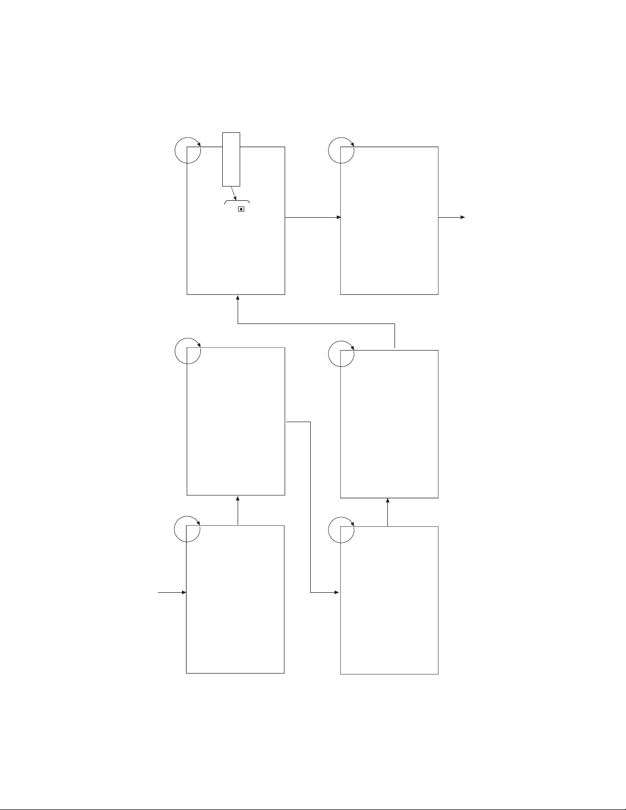
PROTECTION CIRCUIT BLOCK DIAGRAM . . . . . . . . . . . . . . . . . . . . . . . . . . . . . . . .59
BASIC CIRCUIT DIAGRAM . . . . . . . . . . . . . . . . . . . . . . . . . . . . . . . . . . . . . . . . . . . .60
PRINTED CIRCUIT BOARDS . . . . . . . . . . . . . . . . . . . . . . . . . . . . . . . . . . . . . . . . . . .76
BLOCK DIAGRAM . . . . . . . . . . . . . . . . . . . . . . . . . . . . . . . . . . . . . . . . . . . . . . . . . . .90
WIRING DIAGRAM . . . . . . . . . . . . . . . . . . . . . . . . . . . . . . . . . . . . . . . . . . . . . . . . . . .91
CHASSIS WIRING DRAWING . . . . . . . . . . . . . . . . . . . . . . . . . . . . . . . . . . . . . . . . . .93
EXPLODED VIEW . . . . . . . . . . . . . . . . . . . . . . . . . . . . . . . . . . . . . . . . . . . . . . . . . . .94
REPLACEMENT PARTS LIST . . . . . . . . . . . . . . . . . . . . . . . . . . . . . . . . . . . . . . . . . .96
QUICK REFERENCE PARTS LIST . . . . . . . . . . . . . . . . . . . . . . . . . . . . . . . . . . . . . .118
CAUTION: These servicing instructions are for use by qualified service personnel only. To reduce the risk of
electric shock do not perform any servicing other than that contained in the operating instructions
unless you are qualified to do so. Before servicing this chassis, it is important that the service
technician read the “IMPORTANT SAFETY INSTRUCTIONS” in this service manual.
SAFETY NOTICE
USE ISOLATION TRANSFORMER WHEN SERVICING
Components having special safety characteristics are identified by a on the schematics and on the parts list in this
Service Data and its supplements and bulletins. Before servicing the chassis, it is important that the service technician
read and follow the “Important Safety Instructions” in this Service Manual.
PROJECTION COLOR TELEVISION
SPECIFICATIONS AND PARTS ARE SUBJECT TO CHANGE FOR IMPROVEMENT
!
Page 2

2
Components having special safety characteristics are identified by a on the schematics and on the parts list in this service
manual and its supplements and bulletins. Before servicing this chassis, it is important that the service technician read and
follow the “Important Safety Instructions” in this Service Manual.
For continued X-Radiation protection, replace picture tube with original type or Hitachi approved equivalent type.
This Service Manual is intended for qualified service technicians; it is not meant for the casual do-it-yourselfer. Qualified
technicians have the necessary test equipment and tools, and have been trained to properly and safely repair complex
products such as those covered by this manual.
Improperly performed repairs can adversely affect the safety and reliability of the product and may void warranty. If you
are not qualified to perform the repair of this product properly and safely, you should not risk trying to do so and refer the
repair to a qualified service technician.
WARNING
Lead in solder used in this product is listed by the California Health and Welfare agency as a known reproductive toxicant which
may cause birth defects or other reproductive harm (California Health and Safety Code, Section 25249.5).
When servicing or handling circuit boards and other components which contain lead in solder, avoid unprotected skin contact
with solder. Also, when soldering do not inhale any smoke or fumes produced.
This television receiver provides display of television closed captioning in accordance with section 15.119 of the FCC rules.
FEDERAL COMMUNICATIONS COMMISSION NOTICE
This equipment has been tested and found to comply with the limits for a Class B digital device, pursuant to Part 15 of the
FCC Rules. These limits are designed to provide reasonable protection against harmful interference in a residential
installation. This equipment generates, uses, and can radiate radio frequency energy and, if not installed and used in
accordance with the instructions, may cause harmful interference to radio communications. However, there is no guarantee
that interference will not occur in a particular installation. If this equipment does cause harmful interference to radio or
television reception, which can be determined by turning the equipment off and on, the user is encouraged to try to correct
the interference by one or more of the following measures:
¥ Reorient or relocate the receiving antenna.
¥ Increase the separation between the equipment and the receiver.
¥ Connect the equipment into an outlet on a circuit different from that to which the receiver is connected.
¥ Consult the dealer or an experienced radio/television technician for help.
IMPORTANT SAFETY INSTRUCTIONS
USE ISOLATION TRANSFORMER WHEN SERVICING
!
Page 3
3
IMPORTANT SAFETY INSTRUCTION
1. Before returning an instrument to the customer, always
make a safety check of the entire instrument, including
but not limited to the following items.
a. Be sure that no built-in protective devices are
defective and/or have been deleted during servicing.
(1) Protective shields are provided on this chassis to
protect both the technician and the customer.
Correctly replace all missing protective shields,
including any removed for servicing convenience. (2)
When reinstalling the chassis and/or other assembly
in the cabinet, be sure to put back in place all
protective devices, including but not limited to,
nonmetallic control knobs, insulating fishpaper,
adjustment and compartment covers/shields, and
isolation resistor/capacitor networks. Do not operate
this instrument or permit it to be operated without
all protective devices correctly installed and
functioning. Servicers who defeat safety features
or fail to perform safety checks may be liable for
any resulting damage.
b. Be sure that there are no cabinet openings through
which an adult or child might be able to insert their
fingers and contact a hazardous voltage. Such
openings include, but are not limited to (1) spacing
between the picture tube and cabinet mask, (2)
excessively wide cabinet ventilation slots, and (3) an
improperly fitted and/or incorrectly secured cabinet
back cover.
c. Antenna Cold Check Ð With the instrument AC plug
removed from any AC source, connect an electrical
jumper across the two AC plug prongs. Place the
instrument AC switch in the on position. Connect one
lead of an ohmmeter to the AC plug prongs tied
together and touch the other ohmmeter lead in turn to
each tuner antenna input, exposed terminal screw
and, if applicable, to the coaxial connector. If the
measured resistance is less than 1.0 megohms or
greater than 5.2 megohms, an abnormality exists that
must be corrected before the instrument is returned to
the customer. Repeat this test with the instrument AC
switch in the off position.
d. Leakage Current Hot Check Ð With the instrument
completely reassembled, plug the AC line cord
directly into a 120V AC outlet. (Do not use an isolation
transformer during this test.) Use a leakage current
tester or a metering system that complies with
American National Standards Institute (ANSI) C101.0
Leakage Current for Appliances and Underwriters
Laboratories (UL) 1410, (50.7). With the instrument
AC switch first in the on position and then in the off
position, measure from a known earth ground (metal
waterpipe, conduit, etc.) to all exposed metal parts of
the instrument (antennas, handle bracket, metal
cabinet, screw heads, metallic overlays, control
shafts, etc.), especially any exposed metal parts that
offer an electrical return path to the chassis. Any
current measured must not exceed 0.5 milliamps.
Reverse the instrument power cord plug in the outlet
and repeat test.
ANY MEASUREMENTS NOT WITHIN THE LIMITS
SPECIFIED HEREIN INDICATE A POTENTIAL
SHOCK HAZARD THAT MUST BE ELIMINATED
BEFORE RETURNING THE INSTRUMENT TO THE
CUSTOMER OR BEFORE CONNECTING THE
ANTENNA OR ACCESSORIES.
e. High Voltage — This receiver is provided with a hold
down circuit for clearly indicating that voltage has
increased in excess of a predetermined value.
Comply will all notes described in this Service Manual
regarding this hold down circuit when servicing, so
that this hold down circuit may correctly be operated.
f. Service Warning — With maximum contrast, operating
high voltage in this receiver is lower than 31.5 kV. In
case any component having influence on high voltage
is replaced, confirm that the high voltage with
maximum contrast is lower than 31.5 kV.
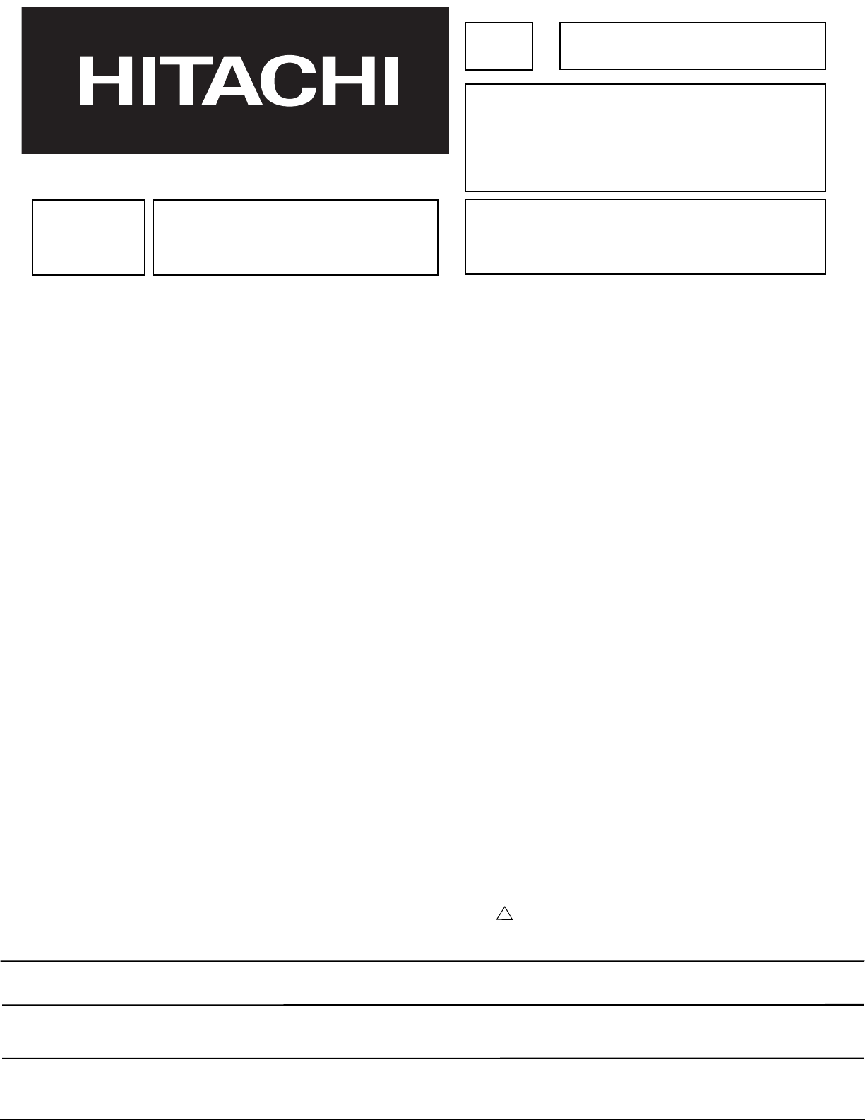
To measure H.V. use a high impedance H.V. meter.
Connect (-) to chassis earth and (+) to the CRT anode
button. (See the following connection diagram.)
Note: Turn power switch off without fail before the
connection to the anode button is made.
LEAKAGE
CURRENT
TESTER
(READING
SHOULD NOT
BE ABOVE 0.5mA)
EARTH
GROUND
TEST ALL
EXPOSED
METAL SURFACES
DEVICE
UNDER
TEST
2-WIRE CORD
ALSO TEST WITH PLUG
REVERSED
(USING AC ADAPTER
PLUS AS REQUIRED)
AC Leakage Test
Chassis
ground
FBT
High Impedance
H.V. meter
Deflection P.W.B.
(TH01)
High voltage
connector
Page 4
4
g. X-radiation – TUBE: The primary source of X-
radiation in this receiver is the picture tube. The tube
utilized for the above mentioned function in this
chassis is specially constructed to limit X-radiation
emissions.
For continued X-radiation protection, the replacement
tube must be the same type as the original, Hitachi
approved type.
When troubleshooting and making test measurements in a receiver with a problem of excessive high
voltage, avoid being unnecessarily close to the picture tube and the high voltage component.
Do not operate the chassis longer than is necessary
to locate the cause of excessive voltage.
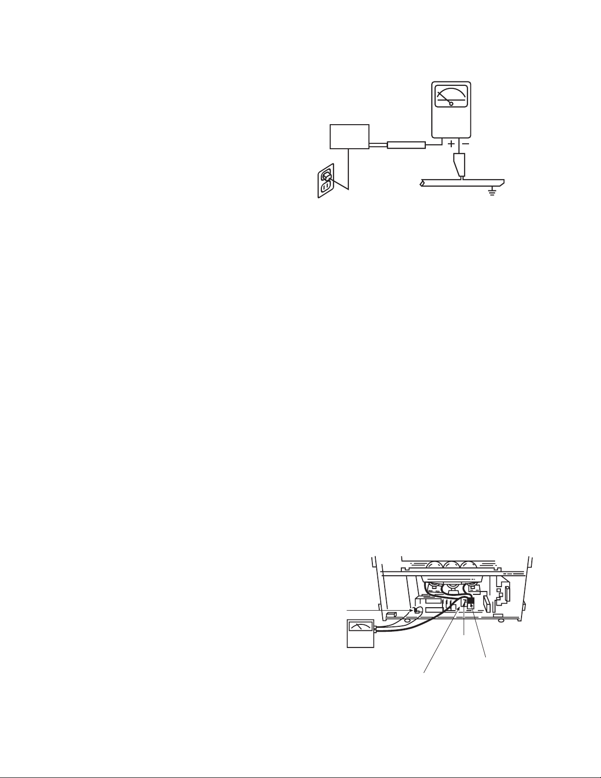
h. X-radiation Shield –
1. This receiver is provided with X-ray shield plates
for protection against X-radiation. Do not remove
X-ray shield plates A, B, or C shown in Fig. 1
unnecessarily, when troubleshooting and/or
making test measurements.
2. To prevent X-radiation, after replacement of
picture tube and lens, confirm these components
to be fixed correctly to bracket and cabinet, and
not to be taken off easily.
Shield Plate A
Glass Lens for Shielding
Shield Plate B
Shield Plate C
Shield Plate D
Detailing X-radiation shield
Shield Plate C
Fig. 1. Installation of shield lens, shield cover and shield plates (oblique view).
IMPORTANT SAFETY INSTRUCTIONS
Page 5

5
2. Read and comply with all caution and safety-related
notes on or inside the receiver cabinet, on the
receiver chassis, or on the picture tube.
3. Design Alteration Warning – Do not alter or add to
the mechanical or electrical design of this TV receiver.
Design alterations and additions including but not
limited to circuit modifications and the addition of
items such as auxiliary audio and/or video output
connectors, might alter the safety characteristics of
this receiver and create a hazard to the user. Any
design alterations or additions may void the
manufacturer’s warranty and may make you, the
servicer, responsible for personal injury or property
damage resulting therefrom.
4. Picture Tube Implosion Protection Warning – The
picture tube in this receiver employs integral
implosion protection. For continued implosion
protection, replace the picture tube only with one of
the same type number. Do not remove, install, or
otherwise handle the picture tube in any manner
without first putting on shatterproof goggles equipped
with side shields. People not so equipped must be
kept safely away while picture tubes are handled.
Keep the picture tube away from your body. Do not
handle the picture tube by its neck.
5. Hot Chassis Warning – a. Some TV receiver chassis
are electrically connected directly to one conductor of
the AC power cord and may be safely serviced
without an isolation transformer only if the AC power
plug is inserted so that the chassis is connected to the
ground side of the AC power source. Confirm that the
AC power plug is inserted correctly with an AC
voltmeter by measuring between the chassis and a
known earth ground. If a voltage reading in excess of
1.0V is obtained, remove and reinsert the AC power
plug in the opposite polarity and again measure the
voltage potential between the chassis and a known
earth ground. b. Some TV receiver chassis normally
have 85V AC (RMS) between chassis and earth
ground regardless of the AC plug polarity. These
chassis can be safely serviced only with an isolation
transformer inserted in the power line between the
receiver and the AC power source, for both personnel
and test equipment protection. c. Some TV receiver
chassis have a secondary ground system in addition
to the main chassis ground. This secondary ground
system is not isolated from the AC power line. The two
ground systems are electrically separated by
insulating material that must not be defeated or
altered.
6. Observe original lead dress. Take extra care to assure
correct lead dress in the following areas: a. near
sharp edges, b. near thermally hot parts – be sure
that leads and components do not touch thermally hot
parts, c. the AC supply, d. high voltage and e. antenna
wiring. Always inspect in all areas for pinched, out-ofplate, or frayed wiring. Do not change spacing
between components and the printed circuit board.
Check AC power cord for damage.
7. Components, parts, and/or wiring that appear to have
overheated or are otherwise damaged should be
replaced with components, parts, or wiring that meet
original specifications. Additionally, determine the
cause of overheating and/or damage and, if
necessary, take corrective action to remove any
potential safety hazard.
8. PRODUCT SAFETY NOTICE – Many TV electrical
and mechanical parts have special safety-related
characteristics some of which are often not evident
from visual inspection, nor can the protection they
give necessarily be obtained by replacing them with
components rated for higher voltage, wattage, etc.
Parts that have special safety characteristics are
identified in Hitachi service data by shading on
schematics and by a in the parts list. Use of
substitute replacement that does not have the same
safety characteristics as the recommended replacement part in Hitachi service data parts list might
create shock, fire, and/or other hazards. Product
safety is under review continuously and new
instructions are issued whenever appropriate. For the
latest information, always consult the appropriate
current Hitachi service literature. A subscription to, or
additional copies of service literature may be obtained
at a nominal charge from Hitachi.
!
IMPORTANT SAFETY INSTRUCTIONS
Page 6

6
CAUTION: Before servicing instruments covered by this
service data and its supplements and addenda, read and
follow the “Important Safety Instructions” on page 3 of this
publication.
NOTE: If unforeseen circumstances create conflict between
the following servicing precautions and any of the safety
precautions on page 3 of this publication, always follow the
safety precautions. Remember: Safety First.
General Servicing Guidelines
1. Always unplug the instrument AC power cord from the AC
power source before:
a. Removing or reinstalling any component, circuit
board, module, or any other instrument assembly.
b. Disconnecting or reconnecting any instrument
electrical plug or other electrical connection.
c. Connecting a test substitute in parallel with an
electrolytic capacitor in the instrument.
CAUTION: A wrong part substitution or incorrect
polarity installation of electrolytic
capacitors may result in an explosion
hazard.
d. Discharging the picture tube anode.
2. T est high voltage only by measuring it with an appropriate
high voltage meter or other voltage measuring device
(DVM, FETVOM, etc.) equipped with a suitable high
voltage probe. Do not test high voltage by “drawing an
arc.” The H.V. Distribution Box has an internal 400MW
resistor (bleeder resistor) connected from the high
voltage to ground. After power is removed from the
instrument the high voltage will discharge through the
high voltage bleeder resistor. If the tubes have high
voltage after power is removed, then the bleeder resistor
is defective or the bleeder ground is disconnected.
3. Discharge the picture tube’s anode at any of the R, G, or
B outputs on the H.V. Distribution Box only by (a) first
connecting one end of an insulated clip lead to the
degaussing or kine aquadag grounding system shield at
the point where the picture tube socket ground lead is
connected, and then (b) touch the other end of the
insulated clip lead to the picture tube high voltage
distribution box R, G, or B output, using an insulated
handle to avoid personal contact with high voltage.
4. Do not spray chemicals on or near this instrument or any
of its assemblies.
5. Unless specified otherwise in these service data, clean
electrical contracts by applying the following mixture to
the contacts with a pipe cleaner, cotton-tipped stick or
comparable nonabrasive applicator: 10% (by volume)
Acetone and 90% (by volume) isopropyl alcohol (90%99% strength).
CAUTION: This is a flammable mixture. Unless
specified otherwise in these service data,
lubrication of contacts is not required.
6. Do not defeat any plug/socket B+ voltage interlocks with
which instruments covered by this service data might be
equipped.
7. Do not apply AC power to this instrument and/or any of its
electrical assemblies unless all solid-state device heatsinks are correctly installed.
8. Always connect the test instrument ground lead to the
appropriate instrument chassis ground before connecting
the test instrument positive lead. Always remove the test
instrument ground lead last.
9. Use with this instrument only the test fixtures specified in
this service data.
CAUTION: Do not connect the test fixture ground strap
to any heatsink in this instrument.
Electrostatically Sensitive (ES) Devices
Some semiconductor (solid state) devices can be damaged
easily by static electricity. Such components commonly are
called Electrostatically Sensitive (ES) Devices. Examples of
typical ES devices are integrated circuits and some fieldeffect transistors and semiconductor “chip” components. The
following techniques should be used to help reduce the
incidence of component damage caused by static electricity.
1. Immediately before handling any semiconductor
component or semiconductor-equipped assembly, drain
off any electrostatic charge on your body by touching a
known earth ground. Alternatively, obtain and wear a
commercially available discharging wrist strap device,
which should be removed for potential shock reasons
prior to applying power to the unit under test.
2. After removing an electrical assembly equipped with ES
devices, place the assembly on a conductive surface
such as aluminum foil, to prevent electrostatic charge
buildup or exposure of the assembly.
3. Use only a grounded-tip soldering iron to solder or
desolder ES devices.
4. Use only can anti-static type solder removal device.
Some solder removal devices not classified as “antistatic” can generate electrical charges sufficient to
damage ES device.
5. Do not use freon-propelled chemicals. These can
generate electrical charges sufficient to damage ES
devices.
6. Do not remove a replacement ES device from its
protective package until immediately before you are
ready to install it. (Most replacement ES devices are
packaged with leads electrically shorted together by
conductive foam, aluminum foil or comparable conductive
material.)
7. Immediately before removing the protective material from
the leads of a replacement ES device, touch the
protective material to the chassis or circuit assembly into
which the device will be installed.
CAUTION: Be sure no power is applied to the chassis or
circuit, and observe all other safety
precautions.
8. Minimize bodily motions when handling unpackaged
replacement ES devices. (Otherwise harmless motion
such as the brushing together of your clothes fabric or the
lifting of your foot from a carpeted floor can generate
SERVICING PRECAUTIONS
Page 7
7
General Soldering Guidelines
1. Use a grounded-tip, low-wattage soldering iron and
appropriate tip size and shape that will maintain tip
temperature within the range 500°F to 600°F.
2. Use an appropriate gauge of resin-core solder composed
of 60 parts tin/40 parts lead.
3. Keep the soldering iron tip clean and well-tinned.
4. Thoroughly clean the surfaces to be soldered. Use a
small wire-bristle (0.5 inch or 1.25 cm) brush with a metal
handle. Do not use freon-propelled spray-on cleaners.
5. Use the following desoldering technique.
a. Allow the soldering iron tip to reach normal
temperature (500°F to 600°F).
b. Heat the component lead until the solder melts.
Quickly draw away the melted solder with an antistatic, suction-type solder removal device or with
solder braid.
CAUTION: Work quickly to avoid overheating the
circuit board printed foil.
6. Use the following soldering technique.
a. Allow the soldering iron tip to reach normal
temperature (500°F to 600°F).
b. First, hold the soldering iron tip and solder strand
against the component lead until the solder melts.
c. Quickly move the soldering iron tip to the junction of
the component lead and the printed circuit foil, and
hold it there only until the solder flows onto and
around both the component lead and the foil.
CAUTION: Work quickly to avoid overheating the
circuit board printed foil or components.
d. Closely inspect the solder area and remove any
excess or splashed solder with a small wire-bristle
brush.
Removal
1. Desolder and straighten each IC lead in one operation by
gently prying up on the lead with the soldering iron tip as
the solder melts.
2. Draw away the melted solder with an anti-static suctiontype solder removal device (or with solder braid) before
removing the IC.
Replacement
1. Carefully insert the replacement IC in the circuit board.
2. Carefully bend each IC lead against the circuit foil pad
and solder it.
3. Clean the soldered areas with a small wire-bristle brush.
(It is not necessary to reapply acrylic coating to areas.)
“Small-signal” Discrete Transistor Removal/Replacement
1. Remove the defective transistor by clipping its leads as
close as possible to the component body.
2. Bend into a “U” shape the end of each of three leads
remaining on the circuit board.
3. Bend into a “U” shape the replacement transistor leads.
4. Connect to replacement transistor leads to the
corresponding leads extending from the circuit board and
crimp the “U” with long nose pliers to insure metal to
metal contact, then solder each connection.
Power Output Transistor Devices Removal/Replacements
1. Heat and remove all solder from around the transistor
leads.
2. Remove the heatsink mounting screw (if so equipped).
3. Carefully remove the transistor from the circuit board.
4. Insert new transistor in circuit board.
5. Solder each transistor lead, and clip off excess lead.
6. Replace heatsink.
Diode Removal/Replacement
1. Remove defective diode by clipping its leads as close as
possible to diode body.
2. Bend the two remaining leads perpendicularly to the
circuit board.
3. Observing diode polarity, wrap each lead of the new
diode around the corresponding lead on the circuit board.
4. Securely crimp each connection and solder it.
5. Inspect (on the circuit board copper side) the solder joints
of the two “original leads”. If they are not shiny, reheat
them and, if necessary, apply additional solder.
Use Solding Iron to Pry Leads
IC Removal/Replacement
Some Hitachi unitized chassis circuit boards have slotted
holes (oblong) through which the IC leads are inserted and
then bent flat against the circuit foil. When holes are the
slotted type, the following technique should be used to
remove and replace the IC. When working with boards using
the familiar round hole, use the standard technique as
outlined in paragraphs 5 and 6 above.
Page 8
8
Fuses and Conventional Resistor Removal/Replacement
1. Clip each fuse or resistor lead at top of circuit board
hollow stake.
2. Securely crimp leads of replacement component around
stake 1/8 inch from top.
3. Solder the connections.
CAUTION: Maintain original spacing between the
replaced component and adjacent
components and the circuit board, to
prevent excessive component
temperatures.
Circuit Board Foil Repair
Excessive heat applied to the copper foil of any printed
circuit board will weaken the adhesive that bonds the foil to
the circuit board, causing the foil to separate from, or “liftoff,” the board. The following guidelines and procedures
should be followed whenever this condition is encountered.
In Critical Copper Pattern Areas
High component/copper pattern density and/or special
voltage/current characteristics make the spacing and
integrity of copper pattern in some circuit board areas more
critical than in others. The circuit foil in these areas is
designated as Critical Copper Pattern. Because Critical
Copper Pattern requires special soldering techniques to
ensure the maintenance of reliability and safety standards,
contact your Hitachi personnel.
At IC Connections
To repair defective copper pattern at IC connections, use the
following procedure to install a jumper wire on the copper
pattern side of the circuit board. (Use this technique only on
IC connections.)
1. Carefully remove the damaged copper pattern with a
sharp knife. (Remove only as much copper as absolutely
necessary.)
2. Carefully scratch away the solder resist and acrylic
coating (if used) from the end of the remaining copper
pattern.
3. Bend a small “U” in one end of a small-gauge jumper wire
and carefully crimp it around the IC pin. Solder the IC
connection.
4. Route the jumper wire along the path of the cut-away
copper pattern and let it overlap the previously scraped
end of the good copper pattern. Solder the overlapped
area, and clip off any excess jumper wire.
1. Remove the defective copper pattern with a sharp knife.
Remove at least 1/4 inch of copper, to ensure hazardous
condition will not exist if the jumper wire opens.
2. Trace along the copper pattern from both wire sides of
the pattern break and locate the nearest component
directly connected to the affected copper pattern.
3. Connect insulated 20-gauge jumper wire from the
nearest component on one side of the pattern break to
the lead of the nearest component on the other side.
Carefully crimp and solder the connections.
CAUTION: Be sure the insulated jumper wire is
dressed so that it does not touch
components or sharp edges.
Frequency Synthesis (FS) Tuning Systems
1. Always unplug the instrument AC power cord before
disconnecting or reconnecting FS tuning system cables
and before removing or inserting FS tuning system
modules.
2. The FS tuner must never be disconnected from the FS
tuning control module while power is applied to the
instrument.
3. When troubleshooting intermittent problems that might be
caused by defective cable connection(s) to the FS tuning
system, remove the instrument AC power as soon as the
defective connector is found and finish confirming the
bad connection with a continuity test. This procedure will
reduce the probability of electrical overstress of the FS
system semi-conductor components.
CRIMP AND
SOLDER
BARE JUMPER
WIRE
Install Jumper Wire and Solder
DEFECTIVE
COPPER
REMOVED
Insulated Jumper Wire
At Other Connections
Use the following technique to repair defective copper
pattern at connections other than IC Pins. This technique
involves the installation of a jumper wire on the component
side of the circuit board.
Page 9

9
Leadless Chip Components
(surface mount)
Chip components must be replaced with identical
chips due to critical foil track spacing. There are no
holes in the board to mount standard transistors or
diodes. Some chip capacitor or resistor board solder
pads may have holes through the board, however the
hole diameter limits standard resistor replacement to
1/8 watt. Standard capacitors may also be limited for
the same reason. It is recommended that identical
chip components be used. .
Chip resistors have a three digit numerical resistance
code -1st and 2nd significant digits and a multiplier.
Example: 162 = 1600 or 1.6KΩ resistor, 0 = 0Ω
(jumper).
Chip capacitors generally do not have the value
indicated on the capacitor. The color of the component
indicates the general range of the capacitance.
Chip transistors are identified by a two letter code. The
first letter indicates the type and the second letter, the
grade of transistor.
Chip diodes have a two letter identification code as
per the code chart and are a dual diode pack with
either
common anode or common cathode. Check the parts
list for correct diode number.
Component Removal
1. Use solder wick to remove solder from component
end caps or terminals.
2. Without pulling up, carefully twist the component
with tweezers to break the adhesive.
3. Do not reuse removed leadless or chip
components since they are subject to stress
fracture during removal .
Chip Component Installation
1. Put a small amount of solder on the board
soldering pads.
2. Hold the chip component against the soldering
pads with tweezers or with a miniature alligator
clip and apply heat to the pad area with a 30 watt
iron until solder flows. Do not apply heat for more
than 3 seconds
How to Replace Flat-lC
—Required Tools—
• Soldering iron • iron wire or small awl
• De-solder braids • Magnifier
1. Remove the solder from all of the pins of a Flat-lC
by using a de-solder braid.
2. Put the iron wire under the pins of the Flat-lC and
pull it in the direction indicated while heating the
pins using a soldering iron. A small awl can be
used instead of the iron wire.
3. Remove the solder from all of the pads of the
Fiat-lC by using
a de-solder braid.
4. Position the new Flat-lC in place (apply the pins of
the Flat-lC to the soldering pads where the pins
need to be soldered). Properly
determine the positions of the
soldering pads and pins by
correctly aligning the polarity
symbol.
6. Check with a magnifier for solder bridge between
the pins or for dry joint between pins and soldering
pads. To remove a solder bridge, use a de-solder
braid as shown in the figure below.
NOTE:
These components are affixed with glue. Be careful not to break or damage any foil under the
component or at the pins of the ICs when removing. Usually applying heat to the component for a short
time while twisting with tweezers will break the component loose.
Chip Components
TYPE
GRADE
C
B
E
SOLDER
CAPS
TRANSISTOR
CAPACITOR
1ST DIGIT
2ND DIGIT
MULTIPLIER
= 1600 = 1.6K
ANODES
MH DIODE
RESISTOR
SOLDER CAPS
COMMON CATHODE
De-Solder
Braid
Soldering
Iron
Soldering
Iron
Soldering
Iron
Soldering
Iron
Soldering
Iron
Soldering
Iron
De-Solder
Braid
Flat-IC
Bridge
Solder
De-Solder
Braid
Iron
Wire
Pull
Awl
Polarity Symbol
5. Solder all pins to the soldering pads using a fine
tipped soldering iron.
Page 10

10
High Voltage limiter circuit operation check.
1. Turn off TV and connect jig as shown in Figure 2.
2. Set the AC input to 120V AC and turn on TV.
3. Confirm test pattern on CRT is a usable picture, then
slowly adjust jig until the picture disappears and TV shuts
down.
4. When the limiter circuit is operating properly, High
Voltage will be less than 31.5 kV at 1.7mAwhen TV shuts
down.
5. Turn off set immediately after checking circuit operation.
6. Unplug set for one minute to reset shutdown circuit.
Remove jig and voltmeter.
TECHNICAL CAUTIONS
(TH01)
Figure 2
Page 11
11
Model: 60DX10B 43GX10B
50DX10B 43GX10B
Cathode-Ray Tube:
50GX30B/43GX10B R=P16LM00EURFA
60DX10B/50DX10B G=P16LFM00EUHHA
B=P16LFM00EUBMB
Power Input: 120 volts AC, 60 Hz
Power Consumption: 189 Watts - Maximum
149 Watts - Operating
1.7 Watts - Stand-by
Antenna Impedance: 75 Ohm Unbalanced
VHF / UHF / CATV
Receiving Channel: BAND CH
VHF 2~13
UHF 14~69
EXT. Mid (A-5)~(A-1), 4+
CATV Mid. A~I
CATV Super J~W
CATV Hyper (W+1)~(W+28)
Intermediate Frequency: Picture l-F Carrier 45.75 MHz
Sound l-F Carrier 41.25 MHz
Color Sub Carrier 42.17 MHz
Video Input: 1 Volt p-p, 75 Ohm
1 Volt p-p, 75 Ohm (Y)
0.7 Volt p-p, 75 Ohm, (P
B
, PR)
Video Output: 1 Volt p-p, 75 ohm
Audio Input: 470 mVrms, 47 k Ohm
Stereo Audio Output: 470 mVrms, 1 k Ohm
Audio Output Power:
Front: 12 watts per channel at 10% distortion,
8 ohm Impedance. Max output Ð 15 watts.
Anode Voltage:
29.5±1.5kv (1.35±0.2mA)
Brightness: 43GX10B 50DX10B 60DX10B
(white screen) 250cd/m
2
205cd/m
2
140cd/m
2
Speakers: 2 Front Speakers
Dimension:
43GX10B 50DX10B/ 60DX10B
50GX30B
Height (in.) 43
3
/
4
52 60
1
/
2
Width (in.) 39 43
1
/
4
61
1
/
2
Depth (in.) 20 23
1
/
2
26
3
/
4
Weight (Ibs.) 143 183 233
Circuit Board Assemblies:
C.P.T. (B) P.W.B. Terminal P.W.B.
C.P.T. (G) P.W.B. VM P.W.B.
C.P.T. (R) P.W.B. Power/Deflection P.W.B.
Control P.W.B. Control Sub P.W.B.
Signal P.W.B. Sensor Distribution P.W.B.
Covergence P.W.B. Trusur/SRS/BBE P.W.B.
CIRCUIT PROTECTION
CAUTION: Below is an EXAMPLE only. See Replacement Parts List for details. The following symbol near the fuse
indicates fast operation fuse (to be replaced). Fuse ratings appear within the symbol.
Example:
SPECIFICATIONS
RISK OF FIRE - REPLACE FUSE AS MARKED
The rating of fuse F901 is 5A - 125V.
Replace with the same type fuse for continued protection
against fire.
F
5 A 125V
125V
5A
Page 12
12
During Insertion
1. Please refer to direction for insertion as shown in Fig. B (L position). Insert connector until “CLICK” sound is heard.
2. Make sure the connector is pressed right in, so that it has a good contact with the spring.
3. Confirm the contact by pulling the connector slightly. (Don’t pull hard because it may damage the connector).
4. Cover the high voltage output by carefully pushing silicon cover onto it. (Don’t turn the connector).
(REMARK)
1. Make sure the silicon cover is
covering the high voltage output.
CAUTIONS WHEN CONNECTING / DISCONNECTING THE HV CONNECTOR
Perform the following when the
HV connector (anode connector)
is removed or inserted for CPT
replacement, etc.
Deflection P.W.B.
Silicon cover
Wing
L Position
L Position
Wing
FBT
Anode
connector
3. Remove the connector slowly
by pulling it away from the
case.
During Removal
1. Roll out silicon cover from FBT’s contact area slowly .
2. While turning the connector about 90 degrees
following the arrow (0 position), push the connector
slightly towards the case. (Fig. A)
Fig. A
Fig. B
Silicon Cover
less than 1mm
PUSH
PUSH
Page 13
13
DIGITAL
ARRAY
POWER
INPUT
EXIT
SELECT
f e b a c
d i j
Push open door and
pull forward and down
PUSH
POWER
INPUT
h
g
EXIT
VOL+VOL-
CH-
CH+
VOL+VOL-
CH-
CH+
MENU
SELECT
MENU
DIGITAL
ARRAY
POWER
EXIT
SELECT
i j
Push open door and
pull forward and down
PUSH
MENU
ab d c
INPUT VOL- VOL+ CH- CH+
FEHG
fgh
POWER
EXIT
SELECT
MENU
INPUT VOL- VOL+ CH- CH+
FEHG
43GX10B/50GX30B
50DX10B/60DX10B
2
3
4
5
1
f
8
7
STOP
CONNECT ONLY 8 OHM SPEAKERS
DO NOT SHORT CIRCUIT
THESE TERMINALS.
(Such damage is NOT COVERED
by your television warranty)
SP. MATRIX
SURROUND
EXT.
R
L
REAR SPEAKER
AUDIO TO HI-FI
VHF/UHF
AUDIO
(MONO)/L
R
AUDIO
(MONO)/L
R
AUDIO
(MONO)/L
R
MONITOR
OUT
INPUT 2
INPUT 1
S-VIDEO
VIDEO
S-VIDEO
VIDEO
VIDEO
AUDIO
R
L
INPUT 4
Y/VIDEO
PB
PR
GENERAL INFORMATION
Fig. 3. Front Control Panel
Fig. 4. Rear Panel Jacks
a Antenna Input/Output g Speaker Matrix Surround Switch
b Audio/Video Inputs 1, 2 h Rear Speaker Terminals
c Monitor Out
d Audio to Hi-Fi
e S-Video Inputs 1 and 2
f Component Input Y-PBP
R
Page 14
14
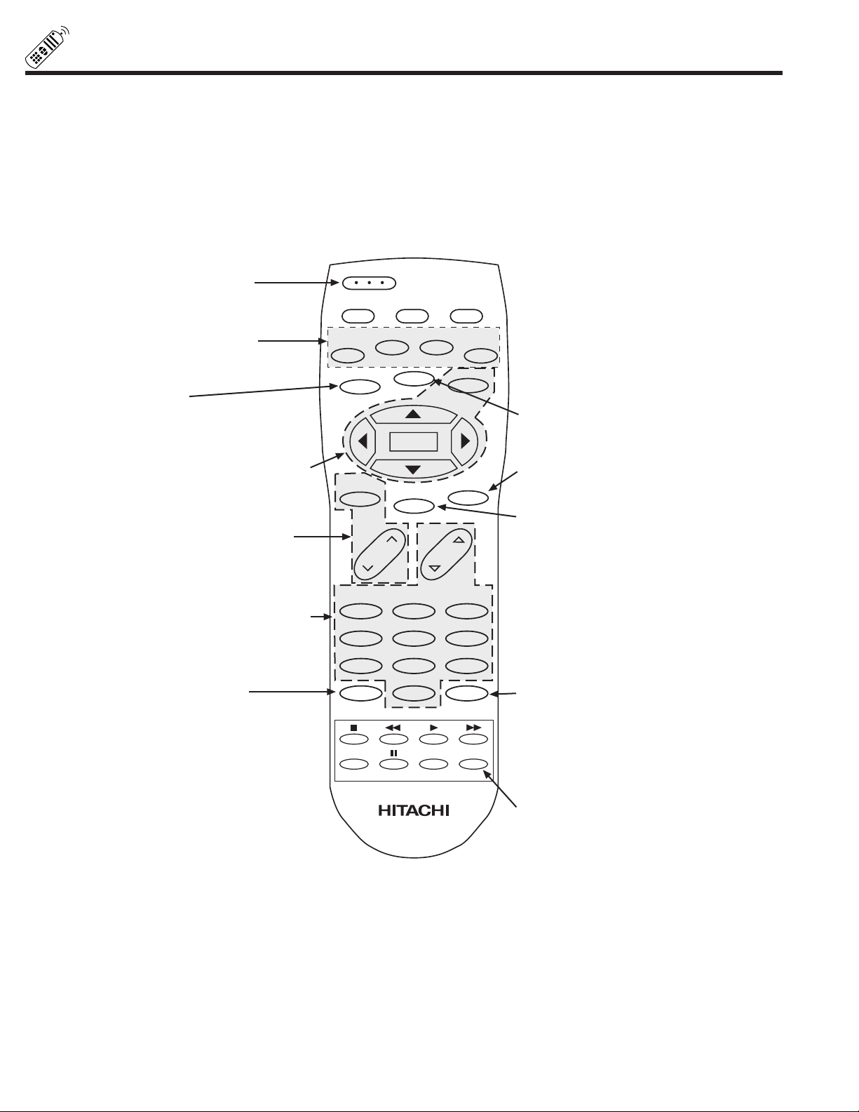
USE THE REMOTE TO CONTROL YOUR TV
VOLUME, MUTE buttons
Use these buttons to obtain the
desired sound level.
123
456
789
0
INPUT
STATUS
VOL CH
POWER
TV CBL/SAT DVD/VCR
PIP
SWAP MOVE
FREEZE
HELP
MENU
MUTE
EXIT
LAST CH
REC
TV/VCR
PIX
SELECT
PIP CH
SELECT, MENU, CURSOR buttons
Use these buttons to set or adjust all
of the On-Screen Display features.
PICTURE-IN-PICTURE
See separate section on pages
23-25 for a detailed description.
HELP button
Press this button to display or cancel
the help messages of the On-Screen
Display.
CHANNEL SELECTOR buttons
Use these buttons to select the
CHANNEL you wish to watch.
INPUT button
Use this button to select the
main or sub-picture video
source from the antenna or
video inputs.
PIP CH button
Use this button to select between
main picture and sub-picture tuning.
a TV POWER button
Press this button to turn
the TV set On or Off
h
k
c
g
d
f
i
EXIT button
Use this button to exit all On-Screen
Display menus.
j
LAST CHANNEL (LAST CH) button
Use this button to select between the last
two channels viewed.
e
STATUS button
Press this button to check the
channel being received, or if it
has Stereo (ST), Second Audio
(SAP), and Channel and Video I.D.
b
PIX button
Press this button repeatedly to
directly access THEATER mode
between Sport, TV, Movies and Music.
l
Page 15
15
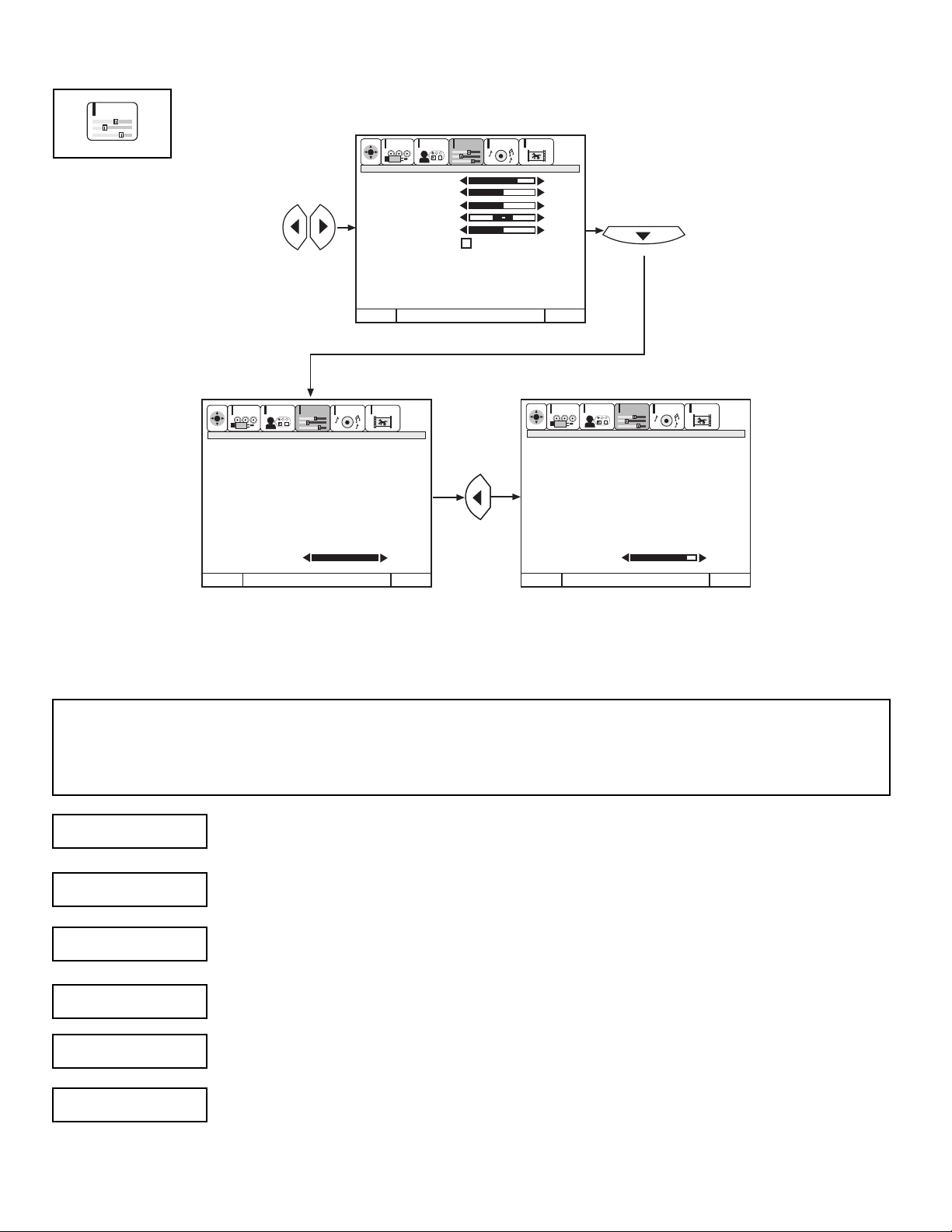
CUSTOMIZED PICTURE AND SOUND ADJUSTMENTS
VIDEO
Select VIDEO to adjust picture settings and improve picture quality.
Use this function to change the contrast between black and white levels in the picture. This adjustment will
only affect the picture when ADVANCED SETTINGS PERFECT PICTURE is OFF. (see page 48)
Use the CURSOR G or H buttons to highlight the function to be adjusted.
Press the CURSOR F or E buttons to adjust the function.
Press EXIT to quit menu.
NOTE: ¥ If CONTRAST is selected, you are adjusting CONTRAST. The additional menu items BRIGHTNESS, COLOR, TINT,
and SHARPNESS can be selected and adjusted in the same manner.
¥ Contrast and Brightness adjustments will affect only the main picture. These adjustments will not affect the sub-picture.
Use this function to adjust the level of color in the picture.
Use this function to adjust flesh tones so they appear natural. (It may be necessary to adjust TINT to obtain
optimum picture quality when using the COMPONENT VIDEO: Y-PBPRINPUT 4 jacks).
Use this function to adjust overall picture brightness.
Use this function to adjust the amount of fine detail in the picture.
When RESET is selected, press SELECT button to return video adjustments to factory preset conditions.
CONTRAST
COLOR
TINT
BRIGHTNESS
SHARPNESS
RESET
Exit
75%
50%
50%
50%
Exit
Contrast
100%
Exit
Contrast
85%
CUSTOMIZE
SETUP
VIDEO
AUDIO
THEATER
SEL
CUSTOMIZE
SETUP
VIDEO
AUDIO
THEATER
SEL
CUSTOMIZE
SETUP
VIDEO
AUDIO
THEATER
SEL
Cursor
Menu To Menu Bar To Quit
Contrast
Brightness
Color
Tint
Sharpness
Reset
Advanced
Settings
Menu To Menu Bar To Quit Menu To Menu Bar To Quit
Cursor
Page 16
16
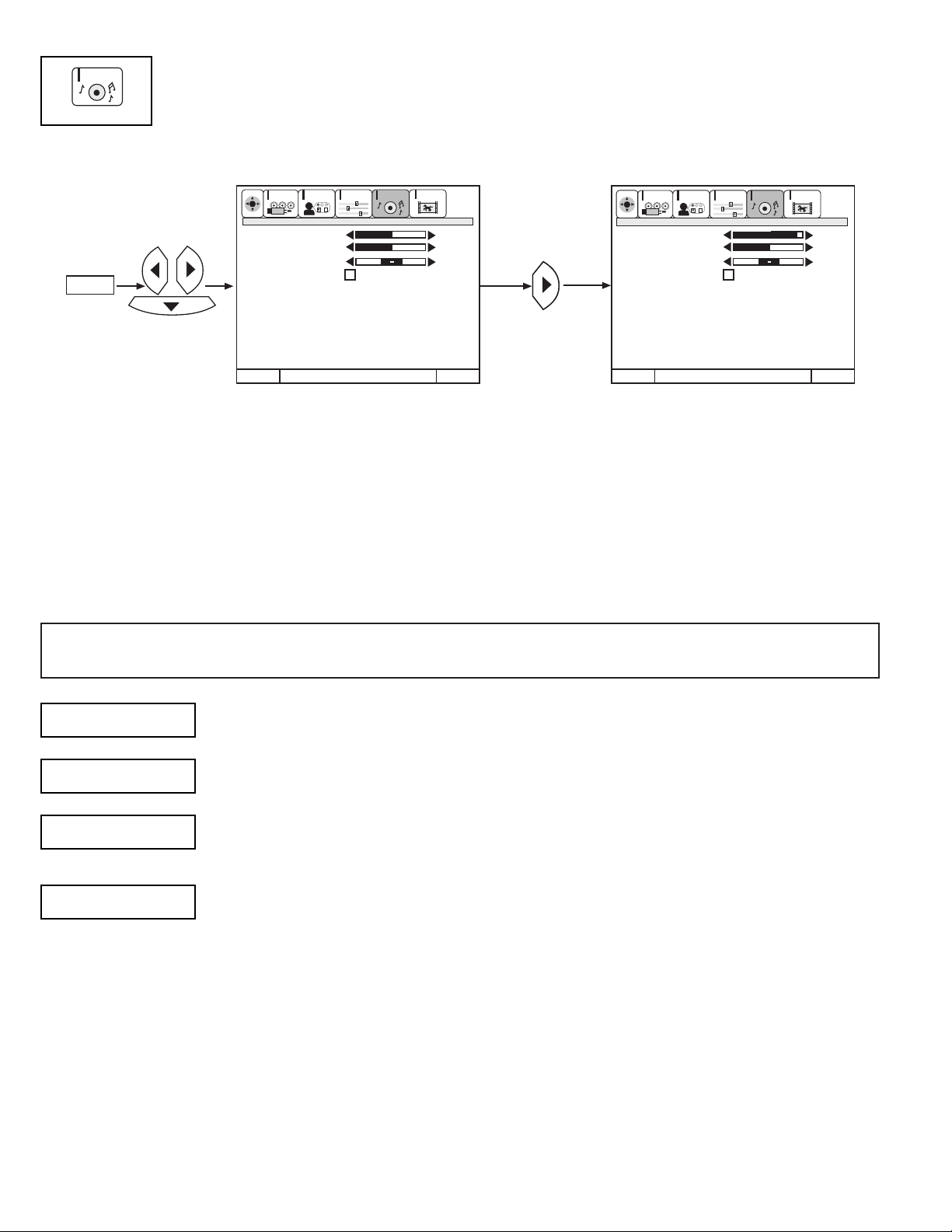
Select AUDIO SETTINGS to adjust the TV to your preference and to improve the sound quality.
This function controls the low frequency audio to all speakers.
Use CURSOR G or H to highlight the function to be adjusted.
Press CURSOR F or E to adjust the function.
Press EXIT to quit MENU.
NOTE: If BASS is selected you are adjusting BASS. The additional menu items TREBLE and BALANCE can be selected and
adjusted in the same manner.
This function controls the high frequency audio to all speakers.
This function will control the left to right balance of the TV internal speakers and the AUDIO TO HI FI output.
When RESET is selected, press SELECT to return audio adjustments to factory preset conditions.
AUDIO
BASS
BALANCE
RESET
TREBLE
ExitExit
90%
50%
BASS
TREBLE
BALANCE
RESET
ADVANCED
SETTINGS
50%
50%
SELECT
CUSTOMIZE
SETUP
VIDEO
AUDIO
THEATER
SEL
CUSTOMIZE
SETUP
VIDEO
AUDIO
THEATER
SEL
Cursor
Menu To Menu Bar To QuitMenu To Menu Bar To Quit
BASS
TREBLE
BALANCE
RESET
ADVANCED
SETTINGS
Page 17
17
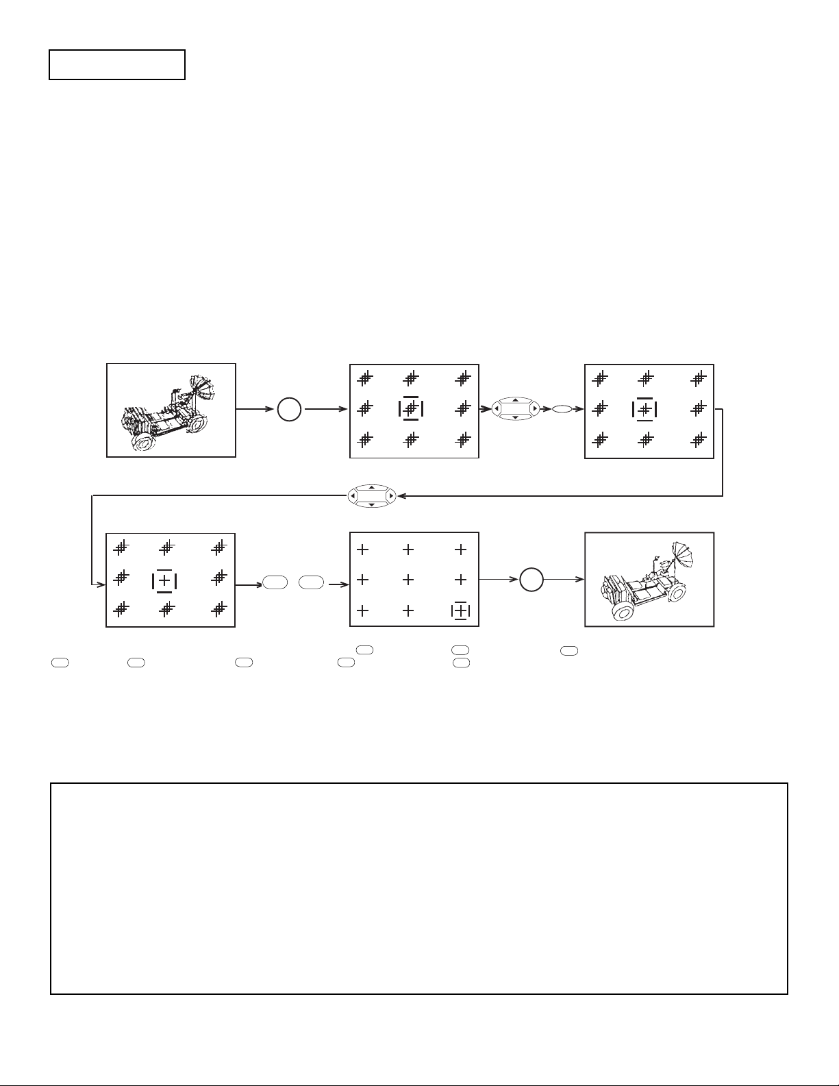
Use the number buttons to select which point to adjust: - Upper Left, - Upper Middle, - Upper Right, - Center Left,
- Center, - Center Right, - Bottom Left, - Bottom Middle, - Bottom Right.
Press the CURSOR buttons to move the displayed color up, down, left, or right.
Press MENU to change the color you want to adjust.
Press the front panel DIGITALARRAY button or the remote control MOVE button when adjustment is done. This will save your
adjustment into memory.
CURSOR
CURSOR
MENU
Your HITACHI Projection TV has three color projection tubes: one for red, one for green, one for blue. When mixed together in the
proper proportion, the output of these three color tubes can produce any color. To produce these colors, however, the beams must be
precisely aligned over each other so that the colors can be mixed. The process of aligning these picture beams is called ÒconvergenceÓ.
Over a period of time, the picture tubes can drift out of alignment due to normal bumps and vibrations or moving the TV. If you move
your TV, or if, after a time, you notice color rings or halos around objects in the picture, you may want to converge (align) the colors.
Properly converged, the lines appear white, which is actually a combination of the outputs of the three color tubes. The output of the
green tube is stationary. The outputs of the red and blue tubes can be adjusted. When properly aligned, the outputs of all three tubes
should be directly over each other to produce the white lines.
To simplify convergence, HITACHI incorporates a feature to allow you to display a test pattern of horizontal and vertical lines at 9
different locations on the screen. Simply use the remote control to adjust the red and blue colors to match the green. When properly
aligned, the outputs of all three tubes should be directly over each other to produce the white lines.
To enter this adjustment mode, you may also select DIGITAL ARRAY from the Set Up menu. However, this will display a message
prompting you to press the front panel DIGITAL ARRAY button.
NOTE: Only a momentary press of the DIGITAL ARRAY button is necessary to enter DIGITAL ARRAY convergence adjustment
mode.
Do not press the DIGITALARRAY button for more than three seconds. This is only for extreme cases of misconvergence
and requires assistance from service.
Four lines surrounding a crosshatch indicate the point being adjusted. The color of these surrounding lines indicates the
color being adjusted.
To save your adjustment data into memory, press the front panel DIGITAL ARRAY button or the remote control MOVE
Button. If you do NOT wish to save your adjustment data into memory, turn the TV OFF or press the remote control PIP
button. When the TV is turned ON again, your old convergence data will be restored.
When adjusting convergence, always start at the center of the screen.
DIGITAL ARRAY
1
2
3
4
5 6
7 8
9
1 ~ 9
DIGITAL
ARRAY
Red
Blue
DIGITAL
Blue
1
9
~
Blue
ARRAY
Page 18
18
REAR PANEL CONNECTIONS
Typical full feature setup. Follow connections that pertain to your personal entertainment system.
STOP
CONNECT ONLY 8 OHM SPEAKERS
DO NOT SHORT CIRCUIT
THESE TERMINALS.
(Such damage is NOT COVERED
by your television warranty)
SP. MATRIX
SURROUND
EXT.
R
L
REAR SPEAKER
AUDIO TO HI-FI
AUDIO
(MONO)/L
R
AUDIO
(MONO)/L
R
AUDIO
(MONO)/L
R
RL
OUTPUT
Y P P
L R
DVD Player,
Laserdisc player, etc.
RB
LR
INPUT
Stereo System Amplifier
2-Way signal splitter
INPUT
V L R
VCR #2VCR #2
Outside antenna or
cable TV coaxial cable
Cable TV Box
OUTPUT
INPUT
VCR #1
OUTPUT
V L R
S-VHS
ANT
IN
MONITOR
OUT
INPUT 2
INPUT 1
S-VIDEO
VIDEO
S-VIDEO
VIDEO
VIDEO
AUDIO
R
L
INPUT 4
Y/VIDEO
P
B
P
R
VHF/UHF
Page 19

19
SERVICE ADJUSTMENTS
1. ASSEMBLED P.W.B ADJUSTMENT..................................................................................................................20
1-1. Memory Initialization (NTSC, SDTV and HDTV) ....................................................................................20
1-2. Comb Filter Operation Check ................................................................................................................25
1-3. Scanning Area Check ............................................................................................................................25
2-0. Final Assembly Adjustment ....................................................................................................................26
2-1. Graphic Equalizer Operation Check ................................................................................................34
2-2. Perfect Volume Operation Check ....................................................................................................34
2-3. Dynamic Bass Operation Check......................................................................................................34
2-4. Input Source Operation Check ........................................................................................................35
2-5. Surround Mode Operation Check....................................................................................................35
2-6. Speaker Setup Operation Check ....................................................................................................37
1-4. High Voltage Adjustment ........................................................................................................................39
2. FINAL ASSEMBLY ADJUSTMENT (Adjustment should be according to below order) ..............................26
2-1. Cut Off ....................................................................................................................................................26
2-2. Raster Inclination Adjustment (Deflection Yoke) ....................................................................................26
2-3. Horizontal AFC Adjustment ....................................................................................................................26
2-4. Lens Focus Adjustment ..........................................................................................................................27
2-5. Static Focus Adjustment ........................................................................................................................28
2-6. Raster Position........................................................................................................................................29
2-7. Vertical Size ..........................................................................................................................................29
2-8. Horizontal Size ......................................................................................................................................29
2-9. Beam Shape ..........................................................................................................................................30
2-10. Static Focus ............................................................................................................................................30
2-11. Blue Focus ..............................................................................................................................................30
2-12. Digital Convergence................................................................................................................................30
2-12-1. Phase Adjustment ......................................................................................................................31
2-12-2. Raster Position ..........................................................................................................................32
2-12-3. Convergence Point ....................................................................................................................32
2-12-4. Digital Convergence Remote Control ........................................................................................32
2-13. Sub-Brightness........................................................................................................................................33
2-14. White Balance ........................................................................................................................................33
2-15. Sub-Picture Adjustment ..........................................................................................................................33
2-16. Sub-Picture Black Level Check ..............................................................................................................33
2-17. Sub-Picture White Balance ....................................................................................................................33
2-18. Sub-Picture Position................................................................................................................................34
3.0 ADJUSTMENT LOCATIONS............................................................................................................................35
3-1. CRT (R)(G)(B), Cabinet Locations..........................................................................................................35
3-2. Main Chassis (Signal P.W.B.) ................................................................................................................36
3-3. Main Chassis (Power/Deflection P.W.B.) ................................................................................................37
3-4. Convergence P.W.B. ..............................................................................................................................38
Page 20
20
1. ASSEMBLED P.W.B. ADJUSTMENT
1.1 Memory Initialization
Adjustment Procedure
(1) Press INPUT key on
Control Panel and then
Power On to access adjustment
mode.
(2) Receive signal on main picture.
(3) Check the OSD according to
table below, using G,H buttons
on Remote Control.
(4) Press EXIT key to exit I
2
C
ADJUST mode.
NOTE: 1. If there is a
different value
than shown in
the table above,
for fixed data,
adjust it using
F E buttons
(only in this case).
2. When exchanging
microprocessor and
TV is turned on for
first time. It requires
initialization of
MEMORY INITIALIZE.
1.3 Sub-Picture (PIP) position adjustment
Adjustment Preparation
(1) Select signal on main picture.
(2) Video settings have to be
at normal condition.
Adjustment Procedure
(1) Press the INPUT and
POWER button on Control
Panel at same time to acces
VIDEO CHROMA ADJUST
mode.
(2) Select HP POSI (Single) and
VP POSI (Single) using H G
buttons.
(3) Adjust the HP POSI (Single)
(HORIZONTAL) and VP POSI
(Single) (VERTICAL) position
using F E buttons.
(4) Press EXIT button to exit I
2
C
ADJUST mode.
(5) Select single PINP mode and
move the sub picture, using the
MOVE button. Distance between
PINP and edge of screen should
be equal when moved. If it is not,
repeat (1)~(5).
B CUT 3F
G CUT 3F
R CUT 3F
G DRV 3F
ADJUST MODE
SERVICE
SUB BRT*
WHITE BAL
R DRV (COOL)* 48
B DRV (COOL)* 37
R CUTOFF (COOL)* 80
G CUTOFF (COOL)* 80
B CUTOFF (COOL)* 80
H POSITION* 12
V POSITION* 00
FACT RESET
CH U/D, INPUT
ADJUST MODE
SERVICE
SUB BRT
WHITE BAL
R DRV (COOL) 48
B DRV (COOL) 37
R CUTOFF (COOL) 80
G CUTOFF (COOL) 80
B CUTOFF (COOL) 80
H POSITION 12
V POSITION 00
FACT RESET
CH U/D, INPUT
Select SERVICE
and press E key
Press EXIT key
(OSD OFF)
CUT OFF ADJUST MODE
ADJUST MODE
SERVICE
SUB BRT
WHITE BAL
R DRV (COOL) 48
B DRV (COOL) 37
R CUTOFF (COOL) 80
G CUTOFF (COOL) 80
B CUTOFF (COOL) 80
H POSITION 12
V POSITION 00
FACT RESET
CH U/D, INPUT
MENU
Select SERVICE
and press E key
Press EXIT key
R DRV 3F
MENU
MENU
MACRO
MACRO
Select SERVICE
and press E key
Press EXIT key
SUB BRT 80
Press Adjust
MACRO
VIDEO SETTINGS
(1) CONTRAST : MIN
(2) COLOR : MIN
VIDEO SETTINGS
(1) CONTRAST : MAX
(2 ) COLOR,TINT,SHARP,BRIGHT:CENER
(3) COLOR TEMP : COOL
ADJUST
(1) Press E to select the R DRV.,
G DRV., R CUT, G CUT, B CUT.
(2) Press E to adjust.
WHITE BALANCE
ADJ. MODE
POWER + INPUT
Adjust in cool
mode only.
Adjust in cool
mode only.
Adjust in cool
mode only.
*: Adjustable data
others: Fixed data (be careful not to change)
Page 21

21
ADJUST MODE
SERVICE
SUB BRT
WHITE BAL
R DRV (COOL) 48
B DRV (COOL) 37
R CUTOFF (COOL) 80
G CUTOFF (COOL) 80
B CUTOFF (COOL) 80
H POSITION 12
V POSITION 00
FACT RESET
CH U/D, INPUT
ADJUST MODE
SERVICE
SUB BRT
WHITE BAL
R DRV (COOL) 48
B DRV (COOL) 37
R CUTOFF (COOL) 80
G CUTOFF (COOL) 80
B CUTOFF (COOL) 80
H POSITION 12
V POSITION 00
FACT RESET
CH U/D, INPUT
SELECT
Adjust in cool
mode only.
Cursor E to
adjust.
Press EXIT to
exit white
balance mode.
Adjust in cool
mode only.
ADJUST MODE
SERVICE
SUB BRT
WHITE BAL
R DRV (WARM) 48
B DRV (WARM) 37
R CUTOFF (WARM) 80
G CUTOFF (WARM) 80
B CUTOFF (WARM) 80
H POSITION 12
V POSITION 00
FACT RESET
CH U/D, INPUT
Do not adjust WHITE BALANCE in
WARM or NTSC mode. Adjust in
COOL mode only.
ADJUST MODE
SERVICE
SUB BRT
WHITE BAL
R DRV (NTSC) 48
B DRV (NTSC) 37
R CUTOFF (NTSC) 80
G CUTOFF (NTSC) 80
B CUTOFF (NTSC) 80
H POSITION 12
V POSITION 00
FACT RESET
CH U/D, INPUT
Adjust in cool
mode only.
ADJUST MODE
SERVICE
SUB BRT
WHITE BAL
R DRV (WARM) 48
B DRV (WARM) 37
R CUTOFF (WARM) 80
G CUTOFF (WARM) 80
B CUTOFF (WARM) 80
H POSITION 12
V POSITION 00
FACT RESET
CH U/D, INPUT
Adjust in cool
mode only.
SELECT
SELECT
SELECT
E
ADJUST MODE
SERVICE
SUB BRT
WHITE BAL
R DRV (NTSC) 48
B DRV (NTSC) 37
R CUTOFF (NTSC) 80
G CUTOFF (NTSC) 80
B CUTOFF (NTSC) 80
H POSITION 12
V POSITION 00
FACT RESET
CH U/D, INPUT
Adjust in cool
mode only.
SELECT
H POSITION ADJ. MODE
Press FE to adjust
V POSITION ADJ. MODE
Press FE to adjust
Press E to set to
Factory settings
MENU
Page 22
22
ADJUST MODE
PIP WHITE BAL
PIP R (COOL)* 2C
PIP G (COOL)* 2C
PIP B (COOL)* 2C
CH U/D, INPUT
Select PIP WHITE BAL.
and press E key
Press EXIT key
SELECT
MACRO
Adjust in cool
mode only.
PIP B 3F
PIP G 3F
PIP R 3F
ADJUST MODE
PIP WHITE BAL
PIP R (WARM) 2C
PIP G (WARM) 2C
PIP B (WARM) 2C
CH U/D, INPUT
Do not adjust PIP WHITE BALANCE
in WARM or NTSC mode. Adjust in
COOL mode only.
ADJUST MODE
PIP WHITE BAL
PIP R (NTSC) 2C
PIP G (NTSC) 2C
PIP B (NTSC) 2C
CH U/D, INPUT
SELECT
MENU
SELECT
ADJUST MODE
VCJ RESET
3DYC RESET
PIP RESET
BBE RESET
MEMORY INIT
I2COPEN
CH U/D, INPUT
MENU
Item Device
VCJ TA1222BN
3DYC uPD64082
PIP SDA9589
BBE NJW1132
Page 23
23
ADJUST MODE
TA1222 (RF)
SUB CONT 1F
SUB COLOR 40
SUB TINT 40
SUB SHARP 38
TOP FO 00
TOF Q 00
COLOR SYS 00
R-Y PHASE 03
R/B LEVEL 00
G/B LEVEL 00
CH U/D, INPUT
ADJUST MODE
TA1222 (RF)
RGB BRIGHT 40
RGB CONT 60
H BLK PHAS 00
V BLK PHAS 00
GPPHS 01
CH U/D, INPUT
ADJUST MODE
TA1222 (VIDEO)
SUB CONT 1F
SUB COLOR 1A
SUB TINT 40
SUB SHARP 38
TOP FO 00
TOF Q 00
COLOR SYS 00
R-Y PHASE 03
R/B LEVEL 00
G/B LEVEL 00
CH U/D, INPUT
ADJUST MODE
TA1222 (480I)
SUB CONT 1F
SUB COLOR 1A
SUB TINT 40
SUB SHARP 38
TOP FO 00
TOF Q 00
COLOR SYS 00
R-Y PHASE 03
R/B LEVEL 00
G/B LEVEL 00
CH U/D, INPUT
ADJUST MODE
TA1222
YG 00
Y DL 00
TXACL 01
COLOR G 00
CLT 00
CDE 01
C TRAP 00
DC POINT 00
DCRATIO 00
CH U/D, INPUT
SELECT
SELECT
MENU
ADJUST MODE
TA1222
DC LIMIT 00
BEP LIMIT 00
BEP POINT1 05
BEP POINT2 00
B.L.S. 00
B.L.C. 01
B.S.G. 00
B.D.L. 00
BSARE 00
WPDL 01
CH U/D, INPUT
MENU
MENU
ADJUST MODE
TA1222 (480I)
S-TRCK 01
AP PEAK F0 00
STR-MD 00
CH U/D, INPUT
ADJUST MODE
TA1222
HI BRT 01
OS ACL 00
OSD-SL 01
WHITE PEAK 00
DABL POINT 00
D ABLE GAIN 07
ABL POINT 05
ABL GAIN 07
COLOR GAIN 15
CH U/D, INPUT
MENU
MENU
MENU
MENU
SELECT
MENU
Page 24
24
ADJUST MODE
uPD64082
DY GAIN 09
DC GAIN 06
YC VAPINV 0B
YC VAPGAIN 05
YHCOR 00
CH U/D, INPUT
MENU
MENU
ADJUST MODE
SDA9589-2
CONTRAST 0F
BRIGHT 00
LM OFFSET 00
YPEAK 03
YCDEL 00
SELDEL 0F
COLOR SUB 10
V OFSET 00
H OFSET 00
CH U/D, INPUT
MENU
ADJUST MODE
SDA9589-2
COLOR SAT (NTSC) 08
HUE (NTSC) 20
ITCPLL (RF) 02
NRIPLL (RF) 02
HFPOSI (SINGLE) 00
VFPOSI (SINGLE) 0F
H P POSI (SINGLE) 37
V P POSI (SINGLE) 18
CH U/D, INPUT
SELECT
ADJUST MODE
SDA9589-2
COLOR SAT (480I) 08
HUE (480I) 20
ITCPLL (VIDEO) 02
NRIPLL (VIDEO) 00
HFPOSI (MV4) 00
VFPOSI (MV4) 0A
H P POSI (MV4) 27
V P POSI (MV4) 0C
CH U/D, INPUT
NJW1132
BBE HIGH 07
BBE LOW 07
V CHIP RATING
POLLING 0F
TIMEOUT 05
STATUS 02
AFC/CLOCK TEST
OSD H POSI **
OSD V POSI **
CH U/D, INPUT
32ms*POLLING DATA
FROM RATING OFF
DETECTIVE COUNT
MENU
MENU
SELF-DIAGNOSIS
RESET START 00
REMOTE POWER 00
MATRIX POWER 00
REMOTE MEM INIT 00
MATRIX MEM INIT 00
ADJUST MEM INIT 00
ADJUST FAC RESET 00
EEP READ ERROR 00
EEP WRITE ERROR 00
LAST EVENT 0000
CH U/D, INPUT
MENU
Page 25

25
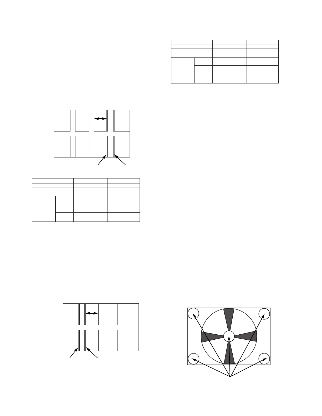
1.2 Comb filter operation check
Adjustment preparation
(1) Receive the color bar signal at the regular tuning
point.
(2) Set the CONTRAST control to MAX and the
other controls to center.
(3) Set the PERFECT PICTURE to OFF.
Adjustment procedure
(1) Check that between the color bars there are line
dots every second color bar as shown in the
drawing.
A
A A
B
LINE DOT
AX
BX
Check and line dots.
B
A
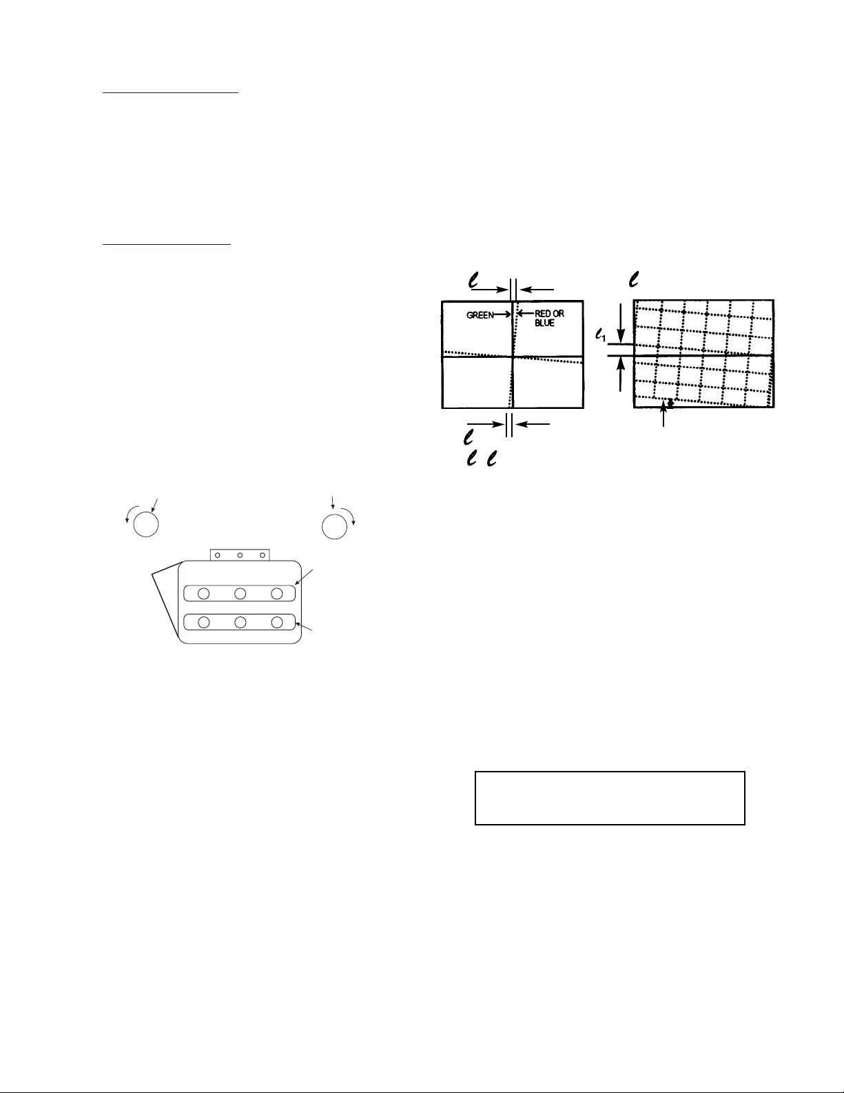
Item Symbol 43Ó 50Ó 60Ó
Top/Bottom pincushion distortion A,B ±5 ±6 ±6
Right/Left pincushion distortion C,D ±4 ±4 ±5
Center line Vertical line E 5 6 6
tilt Horizontal line F 5 6 6
Center line Vertical line G ±3 ±3 ±4
winding Horizontal line H ±3 ±3 ±4
Trapezoidal distortion Vertical line I,J 4 5 5
Skew distortion Horizontal line K,L 5 6 6
(unit: mm)
G
I
J
D
C
A
B
F
E
K
H
L
1.3 Scanning Area Check
Checking Condition
(1) Digital convergence adjustment should have been
completed.
(2) Receive the circle pattern signal.
(3) Brightness/Contrast - Standard condition
Contrast: Max
Other Controls: Center position
(4) Check that the scanning area matches with the next
drawing.
1.3 Raster Distortion Check
Checking Condition
(1) Digital convergence adjustment should have been
completed.
(2) Receive the cross-hatch signal.
(3) Brightness/Contrast - Standard condition
Contrast: Max
Other Controls: Center position
(4) Check the raster distortion.
Specification: Value shown in the table below or
less.
A~D
I~L
- Measure the winding of the outside line.
Page 26
26
2. FINAL ASSEMBLY ADJUSTMENT
2.1 Cut Off Adjustment
Adjustment preparation
(1) Set R and G drive VRÕs on CPT P.W.B. to center.
(2) Adjust screen VRÕs on Focus Pack fully
counterclockwise.
(3) Adjust Focus VRÕs on Focus Pack fully
clockwise.
(4) Set video conditions to factory preset.
(5) The vertical incident illumination on the screen
should be 20 lux or less (room should be dark).
Adjustment procedure
(1) Press and hold INPUT key on control panel and
then POWER ON to access I
2
C adjustment
mode.
(2) Choose “SERVICE” item from I
2
C adjustment
menu by pressing CURSOR E.
(3) Screen VR should be turned clockwise gradually
and set so that retrace line begins to appear.
(4) Return to “NORMAL” mode by pressing the
EXIT button.
(5) The blue line should be lighter thatn red and/or
green.
(6) Adjust Focus VR’s so that focus is even all
around screen.
FOCUS PACK
2.2 Raster Inclination adjustment (Deflection
Yoke)
Adjustment preparation
(1) The set can face east or west.
(2) Input the single cross test signal.
(3) Set video conditions to factory reset.
(4) The lens focus adjustment should have been
completed.
(5) The electric focus should have been coarse
adjusted.
(6) The digital convergence RAM should be cleared
(uncorrected state). With the TV set off, press
and hold the service switch located on the
Power/Deflection PWB and then press the
power button.
(7) Start adjustment 20 minutes or more after TV is
turned on
Adjustment procedure
(1) Apply covers to the R and B lenses and project
only green light.
(2) Turn the G deflection yoke and adjust the vertical
raster inclination.
(3) Then, remove the cover of R or B lens and project
red or blue light and green light together on the
screen.
(4) Turn the deflection yoke of R or B and set so that
the inclination of R or B with respect to the green
light is as shown below on the top and bottom
sides.
(5) After raster inclination adjustment, fixing screw
of DY should be screwed with 12±2kg-cm
torque.
2.3 Horizontal AFC Adjustment
Adjustment preparation
(1) Face the set East or West.
(2) Display the circle pattern signal.
(3) Contrast: Max, Brightness: Center.
(4) The electrical focus should have been coarse-
adjusted.
(5) The convergence should be in un-corrected
state.
Method of no correction state:
Turn power off and press POWER button and
DIGITAL CONV. SERVICE ONLY button at the
same time.
Then convergence is in correction.
NOTE:
DIGITAL CONV. SERVICE ONLY button:
on the CONVER/FOCUS P.W.B.
Adjustment procedure
(1) Project only G on the screen using any one of
the following procedures.
(a) Apply covers to the R and B lenses, or
(b) Short-circuit 2P sub mini connectors of the
R and B CPT P.W.B.
(2) Set the VR of horizontal adjustment R603
counter clockwise, and set the H size minimum.
(3) Check as shown below.
The “0” marker of circle pattern is visible.
NOTE: In the case of inability to see “0” marker, turn
the horizontal size adjustment VR at clockwise
until the marker is visible.
Static Focus VR
R
GB
R
GB
Screen VR
Focus VR
Screen VR
1
, 2 £ ± 2mm
1
1
£ ±2 m m
Notes: (1) If internal cross-hatch does not appear after
clearing RAM data, press service switch
again, on POWER/DEFLECTION PWB.
(2) To restore old RAM data, turn TV off and on.
CROSSHATCH (GREEN)
2
Page 27

27
2.4 LENS FOCUS ADJUSTMENT
Adjustment preparation
(1) The orientation of PTV set is arbitrary, west,
east, north and south.
(2) Centering DY inclination should have been
adjusted.
(3) FOCUS VR location adjustment should have
been completed. (Red : 12 OÕclock, Green : 1~2
OÕclock).
(4) Receive the cross-hatch pattern signal.
(5) Refer to setup below.
CONTRAST : HALF of full scale.
BRIGHTNESS : minimum
Adjustment procedure
(1) Loosen the fixing screw or wing nut on the lens
cylinder so that the lens cylinder can be turned.
(Be careful not to loosen too much). After
completing steps (4), (5), (6) below, tighten the
fixing screws or wing nuts for each lens with a
torque of 1.18N.m (12Kgf cm) ~ 1.67N.m (17Kgf
cm).
(Be careful the lens cylinder does not turn after
having tightened the screw or wing nuts. If it is
tightened too much, lens may tilt or screw may
break.)
(2) Apply covers to each color of R, G and B lenses.
And project a single color on the screen and
adjust in sequence. (The adjustment order of R,
G and B is only an example.)
(3) If the lens adjustment knob is turned clockwise
viewed from the front, the color Aberration
change as follows.
123
0
123
0
*2
*1
(NOTE 1)
Fixing Screw
(NOTE 2)
Fixing Wing Nut
TYPE 1 TYPE 2
Lens Assy
Lens Assy
(4) In case of G lens. Set to the point where the
chromatic aberration switches from blue to red.
If the chromatic aberration appearing all over
the screen is not the same, observe the vertical
bright line and adjust lens focus as specified in
table below. When the red chromatic aberration
appearing at both sides of the bright line is not
equal, observe the side with larger chromatic
aberration when adjusting.
Color
Aberration
Cross-Hatch
Change of Color Aberration
Short focus Long focus
RED LENS Orange Scarlet
GREEN LENS Blue Red
BLUE LENS Purple Green
O
I
L1
L2
Change the signal to the circle pattern and fine
adjust. Observe the corner part of the screen,
especially observe number in the small circle
when adjusting. If the focus performance at the
screen center exceeds the lower limit, it is
acceptable.
Small circle of circle pattern
CHASSIS 43GX10B/50GX10B 50DX10B/60DX10B
SCREEN SIZE 43Ó 50Ó 60Ó 50Ó
L1 and L2
(PITCHES from CENTER) 3.0 3.0 3.0 3.0
L1&L2 * * * *
COLOR * * * *
ABERRATION I 2mm MAX 3mm MAX 3mm MAX 3mm MAX
*******
O 2mm MAX 3mm MAX 3mm MAX 3mm MAX
(NOTE) * Slightly reddish or no color
** Slightly reddish or no color
OPTICAL FOCUSING ADJUSTMENT GREEN
There is no picture fold.
Page 28
28
(5) In case of R lens. Set the position where the
chromatic aberration changes from red to
crimson. As shown below, observe the vertical
bright line and adjust lens focus where the
crimson or red chromatic aberration slightly
appears inside and crimson or red outside
(reference value : 1~3mm) at the point specified
in table below. Change the signal and fine-
adjust in the same way as the G lens.
O
I
L
NOTE: Setting the center between Red and crimson
is optimum.
(6) In case of B lens. Set the position where the
chromatic aberration changes from purple to
green. As shown below, observe the vertical
bright line and adjust lens focus where the
purple or green chromatic aberration slightly
appears inside and purple or green outside
(reference value : 1~3mm) at the point specified
in table below. Change the signal and fine-
adjust in the same way as the G lens.
O
I
L
NOTE: Setting to the center between purple and
crimson is optimum.
Adjustment Procedure
(7) After all colors have been adjusted, display all
colors with the cross-hatch pattern signal and
compare the focus (optical focus) performance
with the limit sample set.
(8) Then, select the circle pattern signal and
compare the focus (optical focus) performance
of each color and all colors together with the
limit sample set.
(9) If the focus performance is worse than the limit
sample set, re-adjust step (1) to (6).
CHASSIS 43GX10B/50GX10B 50DX10B/60DX10B
SCREEN SIZE 43Ó 50Ó 60Ó 50Ó
L1 and L2
(PITCHES from CENTER) 3.0 3.0 3.0 3.0
L1&L2 * * ** **
COLOR * * ** **
ABERRATION I 2mm MAX 3mm MAX 3mm MAX 3mm MAX
** ** * *
O 2mm MAX 3mm MAX 3mm MAX 3mm MAX
(NOTE) * Slightly reddish or no color
** Slightly reddish or no color
CHASSIS 43GX10B/50GX10B 50DX10B/60DX10B
SCREEN SIZE 43Ó 50Ó 60Ó 50Ó
L1 and L2
(PITCHES from CENTER) 3.0 3.0 3.0 3.0
L1&L2 * * ** **
COLOR * * ** **
ABERRATION I 2mm MAX 3mm MAX 3mm MAX 2mm MAX
** ** * *
O 2mm MAX 3mm MAX 2mm MAX 2mm MAX
(NOTE) * Slightly reddish or no color
** Slightly reddish or no color
OPTICAL FOCUSING ADJUSTMENT RED
OPTICAL FOCUSING ADJUSTMENT BLUE
NOTES: 1. Since the G light is very important for
picture quality and performance, pay
special attention in its adjustment.
2. Be careful not to touch the lens with your
fingers when adjusting.
2.5 STATIC FOCUS ADJUSTMENT
Adjustment preparation
(1) LENS FOCUS adjustment should be finished.
(2) Contrast : MAX
Brightness : Center.
(3) Receive the circle pattern signal.
(4) Apply covers to the lens of the colors you are
not adjusting and project only one color on the
screen.
Adjustment procedure
(1) Red and blue static focus adjustment. Adjust
the static focus VR on Focus pack (UFPK) so
that the center of circle pattern is the most clear.
Check that the focus does not get
conspicuously worse at the edges of the circle
pattern signal or cross-hatch signal.
(2) Green static focus adjustment. Adjust the static
focus VR on Focus pack (UFPK) (for green) so
that the center of circle pattern is the most clear.
Check that the focus does not get
conspicuously worse at the checking point, the
periphery of circle pattern cross-hatch signal.
NOTE: Checking point for the periphery of picture.
Checking point
Page 29
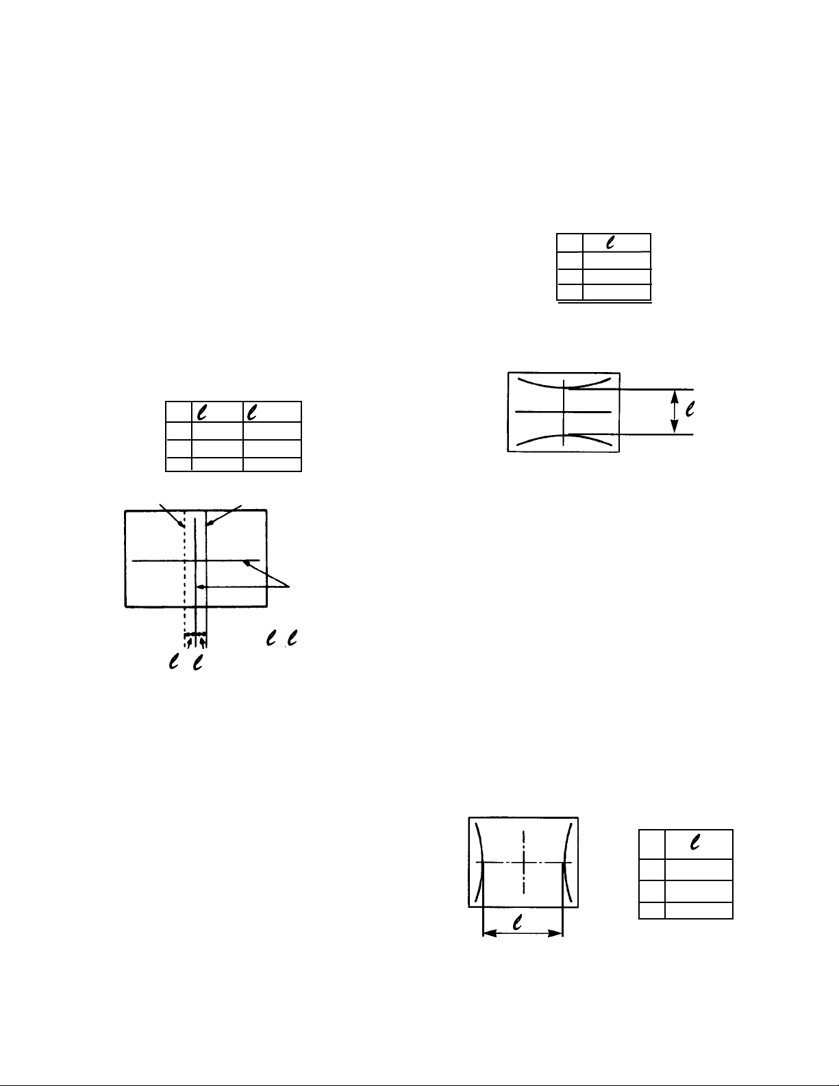
29
Size
60”
50”
43”
2.6 Raster position adjustment
Adjustment preparation
(1) The set can face east or west.
(2) Input the single cross test signal.
(3) Set video conditions to factory reset.
(4) The lens focus adjustment should have been
completed.
(5) The electric focus should have been coarse
adjusted.
(6) The digital convergence RAM should be cleared
(uncorrected state). With the TV set off, press
and hold the service switch located on the
CONVERGENCE PWB and then press the
power button.
(7) Start adjustment 20 minutes or more after TV is
turned on.
Adjustment procedure
(1) Turn the centering magnets for red, green, and
blue to satisfy the condition below. The red and
blue horizontal lines should match with green.
Geometric
center of the
screen
R
B
2.7 Vertical size adjustment (R630)
Adjustment preparation
(1) The set can face east or west.
(2) Input the single cross test signal.
(3) Set video conditions to factory reset.
(4) The lens focus adjustment should have been
completed.
(5) The electric focus should have been coarse
adjusted.
(6) The digital convergence RAM should be cleared
(uncorrected state) . With the TV set off, press
and hold the service switch located on the
CONVERGENCE PWB and then press the
power button.
(7) Start adjustment 20 minutes or more after TV is
turned on.
NOTES: (1) If internal cross-hatch does not appear after
clearing RAM data, press service switch
again.
(2) To restore old RAM data, turn TV off and on.
Size
60” 800 ± 5mm
50” 650 ± 5mm
43” 580 ± 5mm
Note: (1) If internal cross-hatch does not appear after
clearing RAM data, press service switch
again (on POWER/DEFLECTION PWB).
(2) To restore old RAM data, turn TV off and on.
12
1
1,
2
1± 2mm
2
(RED) (BLUE)
10mm 40mm
10mm 30mm
10mm 30mm
Adjustment procedure
(1) Turn only the green by applying covers to the
red and blue lens or shorting the 2 pin TS connectors on the red and blue CPT P.W.B.
(2) Count the vertical lines of the DCU cross hatch.
If the number of vertical lines is 9, go to step (3).
If the number of vertical lines is 8, push “HELP”
key and then “5” key on the R/C so the number
of vertical lines becomes “9”.
(3) Turn vertical amplitude adjustment VR (R630)
so that the distance between the top and bottom
horizontal lines is equal to the size shown in the
table.
2.8 Horizontal size adjustment (R603)
Adjustment preparation
(1) The set can face east or west.
(2) Input the single cross test signal.
(3) Set video conditions to factory reset.
(4) The lens focus adjustment should have been
completed.
(5) The electric focus should have been coarse
adjusted.
(6) The digital convergence RAM should be cleared
(uncorrected state). With the TV set off, press
and hold the service switch located on the
CONVERGENCE PWB and then press the
power button.
(7) Start adjustment 20 minutes or more after TV is
turned on.
Adjustment procedure
(1) Project only green, the same as Vertical size
adjustment.
(2) Turn horizontal amplitude adjustment VR (R603)
so distance between the left and right vertical
lines is equal to the size shown in the table.
Note: (1) If internal cross-hatch does not appear after
clearing RAM data, press service switch
again.
(2) To restore old RAM data, turn TV off and on.
Size
60” 1140 ± 5mm
50” 950 ± 5mm
43” 830 ± 5mm
Page 30
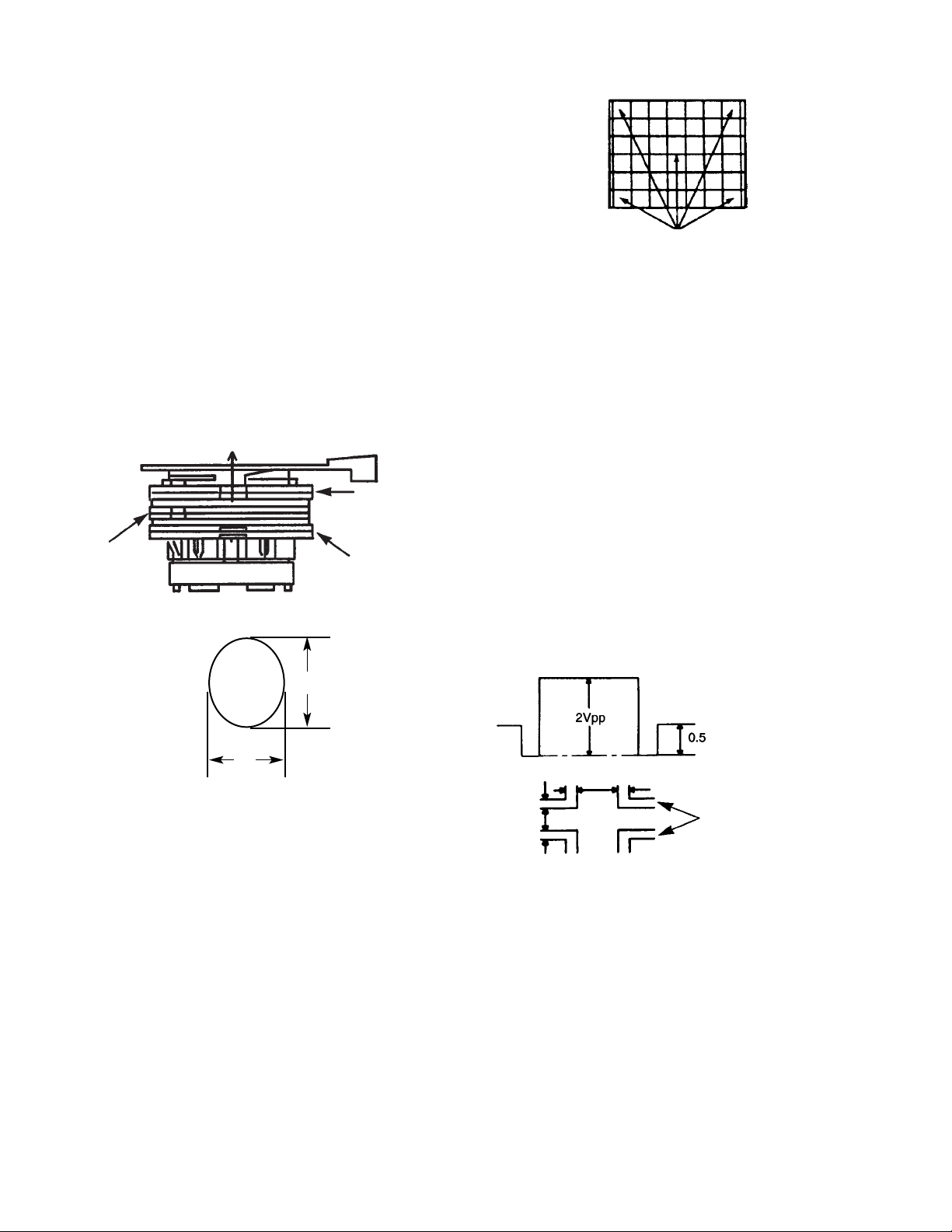
30
2.9 Beam shape adjustment
Adjustment preparation
(1) The beam alignment should have been
completed.
(2) The raster inclination, centering, horizontal/
vertical amplitude and optical focus adjustments
should have been completed.
(3) Set video conditions to factory reset.
(4) Input the dot signal.
Adjustment procedure
(1) Green PRT beam shape adjustment. Short-
circuit 2P sub-mini connectors on Red and Blue
CPT P.W.B.s to project only the Green beam.
(2) Turn the green static focus fully clockwise.
(Blooming.)
(3) Make the dot at the screen center a true circle
using the 4-pole magnet as shown below.
(4) Also adjust the Red and Blue PRT beam shapes
according to the steps (1) to (3).
(5) After the adjustment has been completed, return
R, G and B static VRs to the just focus point.
2.10 Static focus adjustment
Adjustment preparation
(1) The raster inclination, centering, horizontal/
vertical amplitude and optical/electrical focus
beam alignment should have been adjusted.
(2) The static convergence data should be cleared.
(3) Set video conditions to factory reset.
(4) Receive the cross-hatch pattern signal.
(5) Apply covers to the lenses of colors other than
the color to be adjusted and project a single
color.
Adjustment procedure
(1) Red (R), Green (G) and Blue (B) static focus
adjustment. V ary the static focus VR (focus pack
UFPK) and make the center of the cross-hatch
pattern clearest.
(2) Observe the corners of the picture and check
that the focus does not get conspicuously worse.
TRUE CIRCLE SPECIFICATION
TRUE CIRCLE DEGREE:
a/b SPECIFICATION:
PRT SURFACE SIDE
4-POLE BEAM
SHAPE
CORRECTION
2-POLE
BEAM
ZERO FIELD
SPACER (NO
ADJUSTMEN
b
a
OBSERVING POINTS OF THE
CORNER OF THE PICTURE
OBSERVING POINTS
2.11 Blue defocus adjustment
Adjustment Preparation
(1) Optical and electrical focus adjustment should
have been completed.
(2) The convergence adjustment should have been
completed.
(3) Set Video conditions to factory reset.
Adjustment procedure
(1) Input an all-white signal shown below to VIDEO
input.
(2) Short-circuit 2P sub-mini connectors on the red
and green CPT P.W.Bs. to display only the blue
beam.
(3) Turn the B Focus VR (Focus Pack) fully
clockwise.
(4) Measure the brightness at the center of the
screen and turn the B FOCUS VR (Focus Pack)
counterclockwise to adjust the brightness of blue
as shown in Table.
(5) After the adjustment is completed, if blue
exceeds the specification, turn and adjust focus
so that the sticking out part of blue satisfies the
specification.
ALL-WHITE SIGNAL WAVEFORM
TERMINATION CONDITION: OPEN
STICKING OUT OF BLUE
=1mm
Condition: User controls are set to the initial set
positions (for shipment) Measuring point
Screen center.
Cautions: Correct the brightness gauge and amplitude
of the all-white signal periodically. The
aperture angle of the brightness gauge is 1°.
Use a cross-hatch pattern to check.
2.12 Digital convergence adjustment
Adjustment preparation
(1) Receive an RF or video signal.
(2) Set controls to factory preset.
(3) Install jig screen on the set.
(4) Note the center of the video pattern displayed.
This is necessary to match dotted lines
(adjustment point viewed) and actual point that
is adjusted and displayed by the video signal.
Page 31

31
(5) Press the service only switch (on
CONVERGENCE PWB). The pattern displayed
is now the digital convergence mode.
(6) When performing a complete digital
convergence adjustment CLEAR DATAin RAM.
See 2.6. (1) - (7).
Note: If only minor adjustments to convergence are
needed, the jig screen is not necessary. Use
digital data stored in memory and one color as a
reference (red, green, or blue). DO NOT CLEAR
DATAand WRITE to ROM memory.
(2) Identify the bent lines and use the cursor
buttons to move the dotted lines in between as
shown.
(3) Press HELP to exit PHASE mode.
(4) Press EXIT 5 times to display external signal.
(5) Identify center of active video, then press EXIT 5
times to return to internal cross-hatch.
(6) Press HELP (phase adj.), and use 2, 4, 5 and 6
to position internal cross-hatch center on active
video center identified in step (5).
(7) Press HELP to exit PHASE mode.
Adjustment Point
JIG SCREEN SPECIFICATION 43”
ACTIVE
VIDEO
CENTER
FROM
STEP (5)
USE
CURSOR
KEYS TO
MOVE
DOTTED
LINES
BETWEEN
THEN USE NUMBER KEYS TO MATCH INTERNAL
CROSSHATCH CENTER TO ACTIVE VIDEO CENTER
2.12.1 Phase adjustment (service mode)
Adjustment preparation
(1) PHASE adjustment - This is to match the digital
convergence cursor position to the video image
displayed, and to match the digital convergence
cursor position (dotted lines) to digital
convergence data position (bent lines).
Adjustment procedure
(1) Press the HELP button on the remote to select
phase adjustment. (Only Green displayed).
BEFORE
656
874
1.0
72.7
.8
46.8
93.4
46.8
93.4
1.0
72.7
.8
H.SIZE: 830
V.SIZE: 580
10
30
R
B
JIG SCREEN SPECIFICATION 50”
769.2
1020.8
1.0
84.9
1.0
54.8
109.6
54.8
109.6
1.0
84.9
1.0
H.SIZE: 950
V.SIZE: 650
10
30
R
B
JIG SCREEN SPECIFICATION 60”
925.4
1227.2
1.0
102.1
1.0
66.0
131.9
66.0
131.9
1.0
102.1
1.0
H.SIZE: 1140
V.SIZE: 800
10
40
R
B
AFTER
Page 32

32
2.12.4 Digital Convergence Remote Control
Raster Position
123
456
789
0
INPUT
STATUS
VOL CH
POWER
TV CBL/SAT DVD/VCR
PIP
SWAP MOVE
FREEZE
HELP
MENU
MUTE
EXIT
LAST CH
REC
TV/VCR
PIX
SELECT
PIP CH
ROM Write
Remove Color
Initialize
Crosshatch/Video Mode
Cursor Right
Green
(3x3 adj.)
Red
(7x5 adj.)
Blue
(13x9 adj.)
Cursor
Down
Cursor
Left
Cursor
Up
Adjustment
Phase
ROM Read
2.12.2 Raster position adjustment
Adjustment preparation
(1) Position adjustment - This will move an entire
color. Use this adjustment to match colors at the
center of the screen. (Active video center from
external signal and physical screen center
should now match from phase adj. 2.15.1.).
(2) Use the buttons below to switch color to adjust.
“STATUS” - Green
“0” - Red
“INPUT” - Blue
Adjustment procedure
(1) Press the FREEZE button. Extra horizontal lines
appear to confirm raster position mode.
(2) Use the cursor buttons to adjust position.
(3) Press FREEZE again to exit raster position
mode.
Notes: (1) Other functions cannot be accessed when
in raster position adjustment mode. Press
FREEZE and confirm extra horizontal lines
disappear to exit raster position mode.
(2) Press MENU to switch between all colors
displayed or adjustment color and Green
only.
2.12.3 Convergence point adjustment
Adjustment preparation
(1) Select color to adjust.
“STATUS” - Green
“0” - Red
“INPUT” - Blue
(2) Use 4, 6, 2, and 5 to move the cursor position
(dotted lines).
(3) Use cursor buttons to move the convergence
point.
(4) Three adjustment modes are available:
1. (3x3) Press “STATUS” 5 times
2. (7x5) Press “0” 5 times
3. (13x9) Press “INPUT” 5 times
NOTE: 3 x 3 mode can only be accessed at start
of adjustment from clear data in ram adj.
mode.
For touch-up, only the (13x9) mode is necessary.
This will adjust every cross-hatch intersection point
on the screen.
For complete adjustment, start with (3x3) mode. This
will adjust center point and eight edge points only,
but will greatly reduce adjustment time. Then use
(7x5) mode, and finally (13x9) mode to finish
convergence.
Adjustment procedure
(1) Start adjustment at the center of the screen.
(2) Continue adjustment at next closest position.
(3) Adjust center area first, ending with edge
sections.
(4) When convergence is acceptable, press MOVE
to write data to ROM memory. ROM WRITE? is
displayed to alarm system that ROM will be
overwritten with new data. Press the MOVE
button again to write displayed data to ROM.
(5) DATA WRITE TO ROM will take approximately
20 seconds and no picture will be displayed.
(6) Green dots will be displayed when operation is
complete.
(7) Press MUTE to return to convergence pattern,
then confirm again convergence is acceptable.
Notes: (1) Display only green for easier adjustment
and match to jig screen. Press “MENU”,
THEN PRESS “STATUS”.
(2) Write data to ROM after green adjustment.
Once green has been confirmed to match jig
screen, the jig screen can be removed. Do
not readjust the green color after jig screen
has been removed. This is now your
reference color.
(3) Display green and red only and match red to
green.
(4) Display all colors and match blue to green
and red. Touch-up red color if necessary.
(5) Existing DATA in ROM can be read by
pressing the SWAP button 2 times. This
data can be used after replacing a
component (CRT, DY, etc.) Where complete
convergence adjustment is not necessary
be careful not to overwrite this data.
DO NOT save uncorrected RAM data into
ROM or a complete convergence
adjustment will be necessary.
Page 33

33
2.13. SUB BRIGHTNESS ADJUSTMENT
54.1 SUB BRIGHTNESS ADJUSTMENT
Adjustment preparation
(1) Start adjustment 20 minutes or more after the
power is turned ON.
(2) Receive the color bar signal.
(3) The vertical incident illumintation on the screen
should be 20 lux or less.
Adjustment procedure
(1) Go to “Sub Brightness” adj. mode by pressing
INPUT and POWER buttons at the same time.
(2) Adjust Sub Brightness datat to meet spec.
below.
Remarks:
Directly observe the CPT screen by eye, without
using a mirror.
NOTE:
When selecting SUB-BRIGHTNESS mode, the
ucon sets the CONTRAST and COLOR to Min.
automatically, but make sure that the other
conditiions are center.
54.2 CHECK CUT OFF ADJUSTMENT
Adjustment preparation
(1) Pre heat-run should be finished.
Adjustment procedure
(1) Go to “SERVICE” mode by pressing INPUT and
POWER buttons at the same time.
(2) Check that the blue line is lighter than other
lines.
(3) If other lines are lighter than blue line, re-adjust
only Blue Cut OFF in order to be lighter than
other lines.
2.14. WHITE BALANCE ADJUSTMENT
(1) High brightness white balance
(2) Low brightness white balance
Low brightness white balance:
Red : Service mode (R cut OFF)
Green : Service mode (G cut OFF)
Blue : Service mode (B cut OFF) (fix data @
80)
High brightness white balance:
Red : Service mode (R DRV)
Blue : Service mode (B DRV)
Adjustment preparation
(1) Should be started adjustment after 20 minutes
or more form the power turn ON.
(2) Should be finished CUT OFF ADJ>
(3) VIDEO control: Contrast is MAX., Others are
center.
(4) Color temp. : COOL.
(5) Signal:
High Light white balance ADJ.
White raster 0.715Vpp (w/o sync., termination
incidence : 75ohm.)
Low light white balance ADJ.
Luminance should be 20cd/m
2
.
(6) Should be finished BLUE defocus ADJ.
(7) The vertical incident illumination on the screen
should be 20 Lux. or less.
Adjustment procedure
(A) Hight Light W/B adjustment:
(1) Receive signal for High Light white balance
ADJ.
(2) Adjust white balance to 10800K 07 MPCE
(X,Y) = (0.278, 0.280) by using JIG R/C of
(R DRV) and (B DRV0 Screen Center.
(B) Low Light W/B adjustment
(1) Receive signal for Low Light white balance
ADJ.
(2) Adjust white balance to 10800K 07 MPCD
(X, Y) = (0.278, 0.280) by using R/C of (R
CUT OFF) and B CUT OFF should be fixed,
(G CUT OFF).
Repeat A& B two or three times.
* If low light adj. spec. can not be followed,
apply previous adj. spec.
2.15. SUB PICTURE ADJUSTMENT
2.15.1 SUB PICTURE BLACK LEVEL CHECK
Adjustment preparation
(1) Start adjustment about 20 minutes after the
power switch is turned ON.
(2) After displaying the white signal with main
picture, display the sub picture and receive the
clor bar signal with it.
CONDITION: CONT. = MAX.
OTHERS = CENTER
Adjustment procedure
(1) Check the sub picture setting the part of A1 of
the color bar pattern to black.
(check specification ± 0.5 steps.)
2.15.2 SUB PICTURE WHITE BALANCE ADJ.
Adjustment preparation
(1) Turn off the sub picture by pressing (PinP) key of
remote control. (keeping the white signal with
main picture.)
(2) Display and match the sub picture details with
the main picture details by pressing (FRZ) key of
remote controller.
(3) Select “Single” freeze mode.
(4) Condition should be set as follows:
CONT. = MAX.
OTHERS = CENTER
Should sink
to black (A4)
Should rise
slightly from
black (A5)
Y CY G MG R BL
A7 A6 A5 A4 A3 A2 A1
B
C
D
Q I W 100% BLK
W
75%
Page 34

34
(5) Check the EXT RGB CONT : 60 of V/C I2C ADJ.
by using JIG R/C.
(6) White signal spec. amplitude 2.0Vpp (Sync.
0.6Vpp)
Adjustment procedure
(1) Observe P802 on the CPT P.W.B. and change
the PKL B of service mode by using jig R/C and
adjust so that the amplitude of the sub picture is
the same as that of the main picture.
(2) Similarly, observe P832 on the CPT P.W.B. and
change the PKL G of service mode by using jig
R/C and adjust so that the amplitude of the sub
picture is the same as that of the main picture.
(3) Similarly, observe P862 on the CPT P.W.B. and
change the PKL R of service mode by using jig
R/C and adjust so that amplitude of the sub
picture is the same as that of the main picture.
(4) Check the matching the white balance of the
sub picture with that of the main picture.
If it does not, return to step (1).
* Adjustment specification : ±1V
* Quality control specification:
±3V
* Wave form of P802, P832, P862 = Cathode.
(Sub picture levvel compared with main picture
level.)
* Perform this adjustment after the white balance
and sub-brightness adjustments of the main
picture are completed.
* White balance 10800˚K -7 MPCD (color
coordinates : x=0.278, y=0.280)
* Refer to the sub-brightness adjustment for
details of the gray scale of color bar signal.
2.15.3 SUB PICTURE POSITION ADJUSTMENT
Adjustment preparation
(1) Select the Circle Pattern signal on main picture.
(2) Video settings has to be at normal condition
Adjustment procedure
(1) Go to “PinP POSITION ADJ.” mode.
(2) Adjust vertical position and Horizontal position.
NOTE: The micro-controller has an original data for the
PIP position for HP and VP, if the position needs
to be re-adjusted then do the procedure for this
adjustment, in case that the position of PIP is
between the spec. 5.5±0.5 and close to the
lower line of the circle pattern no need to adjust
only checking.
1V
Main Picture
(White)
Sub Picture
(White)
1V
Sub Picture
Center Point
Vertical
SAG
3 5
5 3
Lower Line
Circle Pattern
vp
From Lower Line 5mm
Separation Tolerance
in the lower line
Page 35

3535
3.0 Adjustment Locations
3.1 CRT (R) (G) (B) Cabinet Locations
f
a
e
d
d
b
c
e
1. Centering Magnet for RED PRT.
2. Centering Magnet for GREEN PRT.
3. Centering Magnet for BLUE PRT.
4. 4-Pole Magnet for BEAM FORM ADJSUTMENT
5. BEAM ALIGNMENT Magnet.
6. FOCUS PACK.
FRONT
Page 36

36
0
0
240
0
240
325
240
325
FV
SRS P.W.B.
SIGNAL P.W.B.
FE
FE
U101 U102
VM P.W.B.
I001
I501
SR
SL
TERMINAL P.W.B.
REAR VIEW
3.2 Main Chassis (Signal P.W.B.)
Page 37

3737
0
0
325
0
325
240
T901
R603
REAR VIEW
R630
I601
(FBT)
TH01
T702
3.3 Main Chassis (Power/Deflection P.W.B.)
Page 38

3838
325
0
325
240
REAR VIEW
PCR
PCG
PCB
CONVERGENCE
HEAT
SINK
DIGITAL
CONVERGENCE
UNIT
Page 39

3939
E801
P841
GND
BLUE
E831
P851
GND
GREEN
E861
P801
GND
RED
P852
(CATHODE)
P802
(CATHODE)
RG B
RG B
SCREEN ADJ. VR
FOCUS ADJ. VR
CPT P.W.B.
FOCUS PACK (UFPK)
Page 40

TROUBLESHOOTING
1. No Raster and No Power (REPAIR METHOD)
No raster
Is Power Indicator
Red LED "ON"?
D923
Yes
Check HV-
PROTECT line
D011, D012,
D018
Check
Connector PY1,
I501 etc.
No
Check
DIAGNOSIS
LED's
Is Red LED "ON"?
PROTECTION
D923
Yes
No
How to check DIAGNOSIS LED's.
1. Turn OFF power SW.
2. Turn ON again after several seconds, and carefully observe 3 green LEDs.
Did 3 green LED's
turn OFF same time?
No
A
Yes
B
Find which LED's is going to dark or OFF.
(Other LED's are going to OFF little bit later same time.)
D951(+27V)
Check
+27V line
D914, Q902
IK04, IK05
etc.
D946(+B)
(Change
Brightness, al-
ways on)
Check
+B 120V line
F931, 0777,
I905
40
D947
(30/34V)
Check
Audio 30V
line
D913,
I401 etc.
Page 41

A
Voltage at pin (3) of
Is
I921 5V?
Ye s
Is
Voltage at pin (4) of
I901 10~16V?
Ye s
Has protector
F901 blown
Ye s
Check I901
Replace F901
No
No
No
Check I921,
I904, I902
Check D907, C907,
R905, R906
Check I901
B
Does raster
appear with B and E of
Q914 shorted?
Yes
Check I905, I903, Q903
Q914, Q915, T901 etc.
No
Is base
voltage of
Q701 normal?
Yes
(About AC 0.3V)
Are voltages
of both ends of T701
(primary side)
normal?
Yes (About AC 40V)
No
Check I501
pin (23) -H out
pin (22) -DEF vcc
500mV/Div 10.0µs/Div
v1(1)=.15v v1(2)=2.1v ∆v=1.95v
No
10V/Div 10.0µs/Div
v1(1)=0.0v v1(2)=76v ∆ v=76v
Check I901, D907
Replace F901
41
Check I901, D907
Replace F901
Page 42

2. No Picture
No picture
Is
waveform at pin
41 , 42 , 43 of
I501 normal?
Abnormal
Does on-screen
display appear?
Normal
No
pin 43
2V
1H
pin 42
2.5V
1H
Q517, Q516, Q515
I501, I505, I001, Q002,
Q003, Q007
pin 41
2V
1H
Yes
Is waveform
at pin 2 of
PST2-connector normal?
Abnormal
Is waveform
at pin
16 of
PST-connector normal?
Abnormal
U101 (Front-end)
(Main Tuner)
I201, Q102
1H
1Vp-p
Normal
2Vp-p
Q515
1H
Normal
• IX01, etc.
(2 line Comb)
42
Page 43

3. Reception Impossible with Snow Noise
Main Picture
Reception impossible with snow noise
Is there
output of PLL control
pulse (Clock, Data)
of U101
No
Yes
Is there
voltage applied to pins
Vcc (9v), BP (5v), and
VT (33v) of U101
No
Yes
I001
Sub Picture (PIP)
Reception impossible with snow noise
Is there
output of PLL control
pulse (Clock, Data)
of U102
No
Yes
I504, I505
Is the
LOCK pin of U102
Set to "L"?
No
Is there
voltage applied to pins
Vcc (9v), BP (5v), and
VT (33v) of U102
U101
F/E Main
Yes
U102
(Tuner 2)
Yes
I001
43
No
I504, I505
U102
F/E Sub
Page 44

4. Defective Synchronization
Defective synchronization
Check
Emitter voltage
of Q609
Normal
(26v)
Observe
waveform at pin 31
of I501
Normal
I601
Abnormal (0V)
Abnormal
Q902
Normal
5V p-p
V
I501
44
Page 45

5. Incorrect Color
Incorrect color
When normal
0.6 Vp-p
Color condition
Defective
white balance
Are voltages at
pins 41 , 42 and 43
I501 abnormal?
No color
Yes
Is
chroma signal output
at pin 13 of
I501
No
IX01, etc.
(2 Line Comb.)
1H
Yes
I501, X501, etc.
Does
retrace line appear
with signal color?
Red does
not appear
Q861, Q862
D861, PRT (R)
I501
No No
Are voltages
at 3 , 4 , 5 of
Y1 connector normal?
Yes
Q508, Q509, Q510
Green does
not appear
Q831, Q832
D831, PRT (G)
Blue does
not appear
Q801, Q802
D801, PRT (B)
45
Page 46

6. No Sound
No Sound
Check
voltage at pin 9 of
I401
30V
Is audio signal
input at pins 1 and 30
of IA01?
No
Is audio signal
input at pins 52 and 54
of I201?
No
0V or lower
Yes
Yes
Check Power
Supply Circuit
IA01
Check the I C bus (SCL2, SD A2)
(1) Check the I C bus (SCL1, SD A1)
2
2
I201
U101
46
Page 47

47
I001 Pin 2 I001 Pin 3 I001 Pin 39
I001 Pin 41 I001 Pin 42 I001 Pin 43
I001 Pin 44 I001 Pin 55 I501 Pin 4
I501 Pin 13 I501 Pin 15 I501 Pin 17
1
2
3
4
5
6
7
8
9
10
11
12
WAVEFORMS AT EACH SECTION
Numbers inside circle correspond to locations shown in the circuit diagram.
Page 48

48
I501 Pin 18 I501 Pin 23 I501 Pin 27
I501 Pin 28 I501 Pin 30 I501 Pin 31
I501 Pin 33 I501 Pin 34 I501 Pin 35
I501 Pin 36 I501 Pin 53 I601 Pin 2
22
23
24
19
20
21
16
17
18
13
14
15
WAVEFORMS AT EACH SECTION
Numbers inside circle correspond to locations shown in the circuit diagram.
Page 49

49
I601 Pin 9 I601 Pin 12 PSD1 Pin 5
PSD1 Pin 6 PSD2 Pin 1 PSD2 Pin 2
PSD2 Pin 10 PSD2 Pin 11 Q701 Collector
Q777 Collector Q831 Collector U101 Pin 4
34
35
36
31
32
33
28
29
30
25
26
27
WAVEFORMS AT EACH SECTION
Numbers inside circle correspond to locations shown in the circuit diagram.
Page 50

50
U101 Pin 5 U101 Pin 18
37
38
WAVEFORMS AT EACH SECTION
Numbers inside circle correspond to locations shown in the circuit diagram.
Page 51

Signal (ucon)
DC Voltages
Circuit Pin Voltage Circuit Pin Voltage Circuit Pin Voltage Circuit Pin Voltage
No. No. DC No. No. DC No. No. DC No. Name DC
1 0.0 49 4.9 I004 15 4.0 E 0.0
2 4.8 50 0.0 16 4.9 Q014 B 0.0
3 4.7 51 1.0 1 4.9 C 0.1
4 4.9 I001 52 0.0 I005 2 0.0 E 5.2
5 2.3 53 4.8 3 4.9 Q015 B 5.2
6 2.5 54 0.0 C 0.4
7 4.9 55 0.0 E 4.2
8 4.9 56 4.9
9 3.9 57 4.9
10 3.4 58 0.0 E 0.0 E 13.4
11 0.0 59 4.8 Q002 B 0.1 Q017 B 13.4
12 4.9 60 4.7 C 4.8 C 0
13 4.9 61 4.9 E 0.0 E 13.4
14 4.9 62 2.4 Q003 B 0.7 Q018 B 13.3
15 4.9 63 2.5 C 0.2 C 0.0
16 4.3 64 0.0 E 0.6 E 4.1
17 4.3 1 0.0 Q004 B 0.0 Q019 B 3.5
I001 18 4.9 2 0.0 C 4.9 C 0.0
19 0.0 3 0.0 E 0.0 E 0
20 0.0 I002 4 0.0 Q005 B 0.6 Q021 B 0.2
21 2.3 5 4.8 C 0.0 C 4.3
22 4.9 6 0.0 E 0.0 E 3.1
23 0.0 7 0.0 Q006 B 0.0 Q022 B 3.1
24 2.3 8 4.9 C 4.4 C 0.6
25 1.3 1 0.0 E 0.0 E 4.5
26 2.0 2 3.6 Q007 B 0.0 Q023 B 5.1
27 2.0 3 9.0 C 4.7 C 0.0
28 4.8 I003 4 0.0 E 0.2 E 4.5
29 0.1 5 0.0 Q008 B 0.4 Q024 B 5.2
30 0.0 6 4.2 C 2.5 C 8.9
31 0.6 1 0.2 E 0.2 E 0.0
32 0.6 2 0.0 Q009 B 0.6 Q025 B 0.0
33 2.3 3 0.4 C 2.4 C 4.9
34 3.6 4 0.4 E 5.2 E 0.0
35 0.0 5 0.4 Q010 B 0.0 Q029 B 0.7
36 4.9 6 0.4 C 8.9 C 0.1
37 0.0 I004 7 0.4 E 5.1 E 4
38 0.0 8 0.0 Q011 B 4.9 Q030 B 4.7
39 4.7 9 0.0 C 8.9 C 4.9
40 0.0 10 2.4 E 0.0 E 4.1
41 0.0 11 0.0 Q012 B 0.2 Q031 B 4.7
42 0.0 12 0.0 C 0.0 C 4.9
43 0.0 13 0.0 E 0.0
44 0.0 14 4.8 Q013 B 0.2
45 3.4 C 4.3
46 1.6
47 0.0
48 0.0
Circuit Pin Voltage Q016 B 3.6
No. Name DC C 0.0
51
Page 52

Front End and Audio
Circuit Pin Voltage Circuit Pin Voltage
No. No. DC No. Name DC
1 1.5 E 1.5
2 0.0 Q102 B 2.1
3 0.0 C 9.0
4 0.0 E 1.5
5 1.5 Q103 B 2.2
I401 6 10.7 C 9.0
7 14.4 Q105 B 0.1
8 5.1 C 5.0
9 31.8 E 0.0
10 0.0 Q106 B 0.1
11 4.2 C 5.0
12 14.2
Circuit Pin Voltage
No. Name DC
E 0.0
Q401 B 0.0
C 0.0
E 0.0
Q402 B 0.0
C 0.0
E 0.0
Q403 B 0.0
C 4.4
E 0.0
Q404 B 0.0
C 10.7
DC Voltages
52
Page 53

Video Chroma
DC Voltages
Circuit Pin Voltage Circuit Pin Voltage Circuit Pin Voltage
No. No. DC No. No. DC No. Name DC
1 3.1 49 5.3 E 3.5
2 1.1 I501 50 5.3 Q510 B 2.8
3 4.0 51 4.9 C 0.0
4 2.0 52 4.9 E 3.0
5 2.7 53 6.4 Q511 B 3.6
6 2.7 54 6.0 C 9.0
7 0.0 55 2.9 E 0.0
8 4.1 56 0.0 Q512 B 0.6
9 4.1 1 4.6 C 0.0
10 4.1 2 0.0 E 3.3
11 2.0 3 3.9 Q513 B 3.9
12 4.9 4 0.0 C 9.0
13 2.5 5 3.9 E 0.5
I501 14 0.0 6 0.0 Q514 B 0.0
15 2.6 7 0.1 C 9.0
16 6.4 I502 8 3.0 E 2.4
17 2.5 9 5.0 Q515 B 1.7
18 0.0 10 0.0 C 0.0
19 0.0 11 4.6 E 5.2
20 7.5 12 0.1 Q516 B 4.5
21 0.0 13 9.0 C 0.0
22 9.0 14 4.6 E 0.0
23 1.2 15 0.0 Q517 B 0.0
24 4.5 16 4.6 C 0.0
25 1.5 1 0.1 E 0.0
26 0.0 2 4.5 Q519 B 0.0
27 4.8 I503 3 9.0 C 12.3
28 4.0 4 5.2 E 0.5
29 8.7 5 0.0 Q520 B 0.9
30 0.0 6 5.2 C 10.8
31 4.8 1 0.0 E 0.0
32 0.0 I504 2 0.0 Q521 B 0.0
33 3.5 3 5.0 C 13.4
34 3.5 1 0.0 E 13.5
35 3.5 I505 2 0.3 Q522 B 13.5
36 0.0 3 9.0 C -1.8
37 3.5 E 0.0
38 3.5 Q523 B 0.0
39 3.5 C 0.7
40 8.9
41 2.8
42 2.7
43 2.6
44 0.0
45 5.5
46 8.9
47 0.0
48 3.5
53
Page 54

Deflection
Circuit Pin Voltage Circuit Pin Voltage
No. No. DC No. Name DC
1 11.3 E 8.6
2 4.8 Q602 B 8.0
3 5.6 C 0.9
4 5.8 E 7.9
5 0.0 Q603 B 7.3
I601 6 5.2 C 1.9
7 5.7 E 11.3
8 24.7 Q607 B 10.8
9 1.5 C 8.7
10 1.4 E 25.1
11 0.0 Q609 B 24.8
12 13.2 C 0.0
13 24.4 E 0.5
Q610 B 0.9
C 23.1
E 0.0
Q611 B 0.5
C 23.1
E 23.3
Q612 B 23.1
C 0.0
E 0.0
Q701 B 0.4
C 43.1
E 4.4
Q702 B 4.3
C 12.1
E 8.9
Q703 B 8.3
C 1.9
E 1.9
Q710 B 1.4
C 12.2
E 0.0
Q777 B 0.0
C 121.0
DC Voltages
54
Page 55

DC Voltages
y
Power Suppl
Circuit Pin Voltage Circuit Pin Voltage Circuit Pin Voltage Circuit Pin Voltage
No. No. DC No. No. DC No. No. DC No. No. DC
Convergence
1 2.0 1 1.5 1 8.0 1 0.0
2 0.0 2 0.0 IK01 2 0.0 2 0.0
I901 3 164.3 I907 3 61.6 3 5.0 3 31.4
4 18.9 4 62.7 1 2.5 4 32.5
5 0.0 1 7.8 IK02 2 5.2 5 36.8
1 10.9 I921 2 0.0 3 0.0 6 0.0
2 10.0 3 5.0 7 0.0
I902 3 -10.2 1 25.0 IK04 8 24.6
4 -7.6 I923 2 0.0 9 0.0
1 6.6 3 12.1 10 28.6
2 7.0 1 0.0 11 0.0
I903 3 2.0 I924 2 24.9 12 24.6
4 5.0 3 12.2 13 0.0
1 7.5 14 0.0
2 61.7 15 0.3
3 61.7
4 62.8
Circuit Pin Voltage 16 0.3
No. Name DC 17 24.6
I904 5 216.3 E 67.2 18 0.3
6 0.0 Q909 B 67.2 1 0.0
7 61.7 C 61.5 2 0.0
8 61.7 E 3.3 3 31.3
1 120.0 Q910 B 3.7 4 32.5
I905 2 9.9 C 18.9 5 36.8
3 0.0 E 67.2 6 0.0
Q911 B 33.6 7 0.0
C 61.4 IK05 8 24.6
E 0.0 9 0.0
Q914 B 0.1 10 28.6
C 5.0 11 0.5
E 5.0 12 24.7
Q915 B 5.0 13 0.4
C 0.0 14 0.4
E 0.0 15 0.0
Q931 B 0.8 16 0.0
C 0.4 17 24.6
18 0.0
55
Page 56

DC Voltages
SRS VM
Circuit Pin Voltage Circuit Pin Voltage Circuit Pin Voltage Circuit Pin Voltage
No. No. DC No. No. DC No. Name DC No. Name DC
1 4.5 1 5.0 E 0.8 E 1.2
2 0.0 2 0.0 QE01 B 1.5 QE05 B 1.9
3 0.0 3 5.0 C 7.5 C 13.3
4 4.5 4 0.0 E 2.1 E 14.0
5 0.0 IA07 5 5.0 QE02 B 2.8 QE06 B 14.0
6 0.0 6 5.0 C 6.0 C 24.7
7 4.5 7 5.0 E 0.0 E 14.0
8 0.0 8 9.0 QE03 B 6.0 QE07 B 0.0
9 1.0 C 12.2 C 0.0
10 4.5 E 1.3 E 116.2
11 1.3 QE04 B 2.0 QE08 B 115.5
12 1.3
13 4.9
IA01 14 3.7 E 1.4 QE09 B 0.8
15 0.0 QA01 B 2.1 C 57.3
16 9.0 C 8.3 E 0.0
17 0.0 E 9.0 QE10 B 0.0
18 0.0 QA02 B 8.3 C 0.0
19 0.0 C 0.0 E 1.6
20 1.4 E 1.5 QE11 B 2.1
21 4.5 QA03 B 2.1 C 12.2
22 4.4 C 8.3 E 14.1
23 4.5 E 9.0 QE12 B 13.9
24 4.5 QA04 B 8.3 C 0.0
25 4.5 C 4.8
26 4.5 E 0.0
27 4.5 QA05 B 0.0
28 0.0 C 0.0
29 0.0 E 0.0
30 4.5 QA06 B 0.0
Circuit Pin Voltage C 4.9 C 57.4
No. Name DC E 0.2
C 0.0
56
Page 57

DC Voltages
3DYC and PinP CPT Focus
Circuit Pin Voltage Circuit Pin Voltage Circuit Pin Voltage
No. No. DC No. Name DC No. Name DC
1 1.4 E 11.5 E 1.9
2 1.4 Q801 B 12.4 QF01 B 7.8
3 0.0 C 145.9 C 0.0
4 0.2 E 3.2 E 1.5
5 0.0 Q802 B 3.6 QF03 B 2.1
6 4.1 C 11.4 C 5.2
7 3.3 E 11.4 E 5.5
8 0.0 Q803 B 11.5 QF04 B 5.2
9 3.3 C 12.1 C 0.8
10 0.3 E 3.0 E 0.2
11 0.4 Q804 B 3.2 QF05 B 0.7
12 0.4 C 3.2 C 11.5
13 0.4 E 1.9 E 11.8
IG02 14 0.0 Q805 B 2.6 QF06 B 12.1
15 0.4 C 12.1 C 288.9
16 0.4 E 2.6 E 441.4
17 0.4 Q806 B 1.9 QF07 B 109.5
18 0.0 C 0.0 C 1093.8
19 3.2 E 11.6 E 11.2
20 0.0 Q831 B 12.1 QF08 B 11.7
21 3.3 C 160.0 C 657.5
22 3.2 E 3.0 E 0.3
23 0.0 Q832 B 3.5 QF09 B 0.9
24 0.1 C 11.4 C 8.3
25 1.2 E 11.4 E 8.7
26 0.6 Q833 B 11.6 QF10 B 8.3
27 2.1 C 12.1 C 0.0
28 1.9 E 11.5 E 8.7
Q861 B 12.1 QF11 B 8.8
C 170.8 C 12.1
E 2.9 E 4.6
Circuit Pin Voltage Q862 B 3.4 QF12 B 5.1
No. Name DC C 11.4 C 12.2
E 0.7 E 11.4 E 0.9
QG01 B 0.0 Q863 B 11.4 QF13 B 1.5
C 0.0 C 12.1 C 5.1
E 0.7 E 8.4
QG02 B 0.0 QF14 B 0.0
C 0.0 C 12.1
E 0.7 E 9.0
QG03 B 0.0 QF15 B 9.4
C 0.0 C 12.1
E 0.0
QG04 B 0.7
C 0.2
57
Page 58

DC Voltages
Terminal
Circuit Pin Voltage Circuit Pin Voltage Circuit Pin Voltage Circuit Pin Voltage
No. No. DC No. No. DC No. Name DC No. Name DC
1 0 E 3.5 E 0.0 E 2.3
2 2.3 QX01 B 4.2 Q203 B 4.2 Q211 B 3.0
3 0 C 8.9 C 8.9 C 8.9
4 2.4 E 8.9 E 8.9 E 3.4
5 0 QX02 B 8.2 Q206 B 0.0 Q214 B 0.0
6 0 C 4.2 C 3.4 C 8.9
7 0 E 1.8 E 2.2 E 3.5
IX01 8 0 QX03 B 2.4 Q207 B 2.8 Q215 B 4.2
9 0 C 8.2 C 8.2 C 8.8
10 2.3 E 3.1 E 2.5 E 3.6
11 2.2 QX04 B 3.8 Q208 B 3.1 Q216 B 4.3
12 3.4 C 0.0 C 8.2 C 8.8
13 0 E 2.8 E 8.9 E 3.3
14 0 QX05 B 3.5 Q209 B 8.2 Q217 B 4.0
15 3.5 C 8.9 C 3.5 C 8.9
16 0 E 2.1 E 2.9 E 3.1
QX06 B 2.8 Q210 B 3.5 Q218 B 2.5
C 8.2 C 8.9 C 0.0
E 8.9 E 0.5
Circuit Pin Voltage QX07 B 8.2 Q219 B 1.1
No. No. DC C 4.4 C 0.0
E 2.4 E 3.8 E 0.0
QG13 B 1.7 QX08 B 4.4 Q220 B 0.5
C 0.0 C 8.9 C 4.9
E 0.0 E 5.4 E 0.0
QG15 B 0.7 QX09 B 6.1 Q224 B 0.0
C 0.1 C 8.9 C 0.0
E 0.0 E 1.4 E 0.0
QG16 B 0.1 QX10 B 2.1 Q225 B 0.2
C 1.3 C 8.9 C 0.0
E 0.0
QG17 B 0.0
C 0.1
E 0.0
QG18 B 0.1
C 1.7
58
Page 59

HP1X PROTECTION CIRCUIT BLOCK DIAGRAM
59
AC Plug
Fuse
FP01 6A
Line Filter
LP01
IC Power Monitor
LED (RED): D923
Swithing
Control
I901
Fuse
F901 4A
Rectifier
D901
LIVE COLD
T901
Switching
Transformer
Relay
S901
Feed Back
I902
Rectifier
+30V:D913
Rectifier
+27V:D914
Rectifier
-23V:D915
Rectifier
+11V:D973
Rectifier
+7V:D916
Rectifier
+120V:D929
D948: +30V
D951: +27V
Regulator
+26V:Q902
Regulator
-12V:I923
Regulator
+9V:I505
Rectifier
+5V:I504
Voltage Control
I905
Regulator
+12V:I923
D946: +120V
D946: <6V
D964:<4V
D963: -22V
D521: <3V
D522: <1V
Audio:
SW +30V
SW +27V
SW +26V
SW +12V
SW -23V
SW-12V
SW +11V
SW +9V
SW +5V
D952: >44V
ZD
D950: >27V
ZD
D607>18V
ZD
D952: >5V
ZD
D
D
ZD
D
D
Q903: >1.38A
Q
Protector
F931 2K
D933: >150V
ZD
Over Voltage
Detector
Short CCT
Dectector
+120V
Rectifier
D909/D910
Fuse
F902 1A
Switching
Control
I904
T902
Switching
Transformer
Feed Back
I907
AC Clock
I903
Rectifier
D937
AC Clock 60Hz
Protect ON/OFF
Q914
Power ON/OFF
Q931
Regulator
I922
OFF
ON
ON
OFF
Power
ON/OFF
=RED or GREEN
Protect DET
I001
X-Ray Protect
SBY -5V
Page 60

44KHz
1 234
5
6
A
B
C
D
E
O All DC voltage to be measured with a tester (100kh/V). Voltage taken on a complex color bar signal including a standard color bar signal.
O Since this is a basic circuit diagram, the value of the parts is subject to be altered for improvement.
POWER SUPPLY
PRODUCT SAFETY NOTE: Components marked with a and shaded have special characteristics important to
safety. Before replacing any of these components, read carefully the PRODUCT SAFETY NOTICE of this Service
Manual. DonÕt degrade the safety of the receiver through improper servicing.
POWER SUPPLY
HP1X CHASSIS
60
BASIC CIRCUIT DIAGRAM
Page 61

34
33
24
25
26
1 234
5
6
A
B
C
D
E
O All DC voltage to be measured with a tester (100kh/V). Voltage taken on a complex color bar signal including a standard color bar signal.
O Since this is a basic circuit diagram, the value of the parts is subject to be altered for improvement.
DEFLECTION
PRODUCT SAFETY NOTE: Components marked with a and shaded have special characteristics important to
safety. Before replacing any of these components, read carefully the PRODUCT SAFETY NOTICE of this Service
Manual. DonÕt degrade the safety of the receiver through improper servicing.
BASIC CIRCUIT DIAGRAM
DEFLECTION
HP1X CHASSIS
61
Page 62

1
2
8
7 6
5
4
3
1 234
5
6
A
B
C
D
E
O All DC voltage to be measured with a tester (100kh/V). Voltage taken on a complex color bar signal including a standard color bar signal.
O Since this is a basic circuit diagram, the value of the parts is subject to be altered for improvement.
UCON
PRODUCT SAFETY NOTE: Components marked with a and shaded have special characteristics important to
safety. Before replacing any of these components, read carefully the PRODUCT SAFETY NOTICE of this Service
Manual. DonÕt degrade the safety of the receiver through improper servicing.
BASIC CIRCUIT DIAGRAM
UCON
HP1X CHASSIS
62
pg. 64
pg. 65
50/60DX10B pg. 75
others pg. 74
Page 63

36
37
38
1 234
5
6
A
B
C
D
E
O All DC voltage to be measured with a tester (100kh/V). Voltage taken on a complex color bar signal including a standard color bar signal.
O Since this is a basic circuit diagram, the value of the parts is subject to be altered for improvement.
F/E AND AUDIO
PRODUCT SAFETY NOTE: Components marked with a and shaded have special characteristics important to
safety. Before replacing any of these components, read carefully the PRODUCT SAFETY NOTICE of this Service
Manual. DonÕt degrade the safety of the receiver through improper servicing.
BASIC CIRCUIT DIAGRAM
F/E AND AUDIO
HP1X CHASSIS
63
pg. 65
pg. 64
Page 64

23
9
10
11
12 14
13
15
16
22
20
18
21
19
17
27
28
29
30
31
32
1 234
5
6
A
B
C
D
E
O All DC voltage to be measured with a tester (100kh/V). Voltage taken on a complex color bar signal including a standard color bar signal.
O Since this is a basic circuit diagram, the value of the parts is subject to be altered for improvement.
VIDEO CHROMA
PRODUCT SAFETY NOTE: Components marked with a and shaded have special characteristics important to
safety. Before replacing any of these components, read carefully the PRODUCT SAFETY NOTICE of this Service
Manual. DonÕt degrade the safety of the receiver through improper servicing.
BASIC CIRCUIT DIAGRAM
VIDEO CHROMA
HP1X CHASSIS
64
pg. 65
pg. 62
pg. 63
pg. 65
Page 65

1 234
5
6
A
B
C
D
E
O All DC voltage to be measured with a tester (100kh/V). Voltage taken on a complex color bar signal including a standard color bar signal.
O Since this is a basic circuit diagram, the value of the parts is subject to be altered for improvement.
3DYC/PinP
PRODUCT SAFETY NOTE: Components marked with a and shaded have special characteristics important to
safety. Before replacing any of these components, read carefully the PRODUCT SAFETY NOTICE of this Service
Manual. DonÕt degrade the safety of the receiver through improper servicing.
BASIC CIRCUIT DIAGRAM
3DYC/PinP
HP1X CHASSIS
65
pg. 63
pg. 64
pg. 62
pg. 64
Page 66

1 234
5
6
A
B
C
D
E
O All DC voltage to be measured with a tester (100kh/V). Voltage taken on a complex color bar signal including a standard color bar signal.
O Since this is a basic circuit diagram, the value of the parts is subject to be altered for improvement.
TERMINAL
PRODUCT SAFETY NOTE: Components marked with a and shaded have special characteristics important to
safety. Before replacing any of these components, read carefully the PRODUCT SAFETY NOTICE of this Service
Manual. DonÕt degrade the safety of the receiver through improper servicing.
BASIC CIRCUIT DIAGRAM
TERMINAL
HP1X CHASSIS
66
Page 67

1 234
5
6
A
B
C
D
E
O All DC voltage to be measured with a tester (100kh/V). Voltage taken on a complex color bar signal including a standard color bar signal.
O Since this is a basic circuit diagram, the value of the parts is subject to be altered for improvement.
CONVERGENCE
PRODUCT SAFETY NOTE: Components marked with a and shaded have special characteristics important to
safety. Before replacing any of these components, read carefully the PRODUCT SAFETY NOTICE of this Service
Manual. DonÕt degrade the safety of the receiver through improper servicing.
BASIC CIRCUIT DIAGRAM
CONVERGENCE
HP1X CHASSIS
67
Page 68

1 234
5
6
A
B
C
D
E
O All DC voltage to be measured with a tester (100kh/V). Voltage taken on a complex color bar signal including a standard color bar signal.
O Since this is a basic circuit diagram, the value of the parts is subject to be altered for improvement.
FOCUS
PRODUCT SAFETY NOTE: Components marked with a and shaded have special characteristics important to
safety. Before replacing any of these components, read carefully the PRODUCT SAFETY NOTICE of this Service
Manual. DonÕt degrade the safety of the receiver through improper servicing.
BASIC CIRCUIT DIAGRAM
FOCUS
HP1X CHASSIS
68
Page 69

1 234
5
6
A
B
C
D
E
O All DC voltage to be measured with a tester (100kh/V). Voltage taken on a complex color bar signal including a standard color bar signal.
O Since this is a basic circuit diagram, the value of the parts is subject to be altered for improvement.
VM
PRODUCT SAFETY NOTE: Components marked with a and shaded have special characteristics important to
safety. Before replacing any of these components, read carefully the PRODUCT SAFETY NOTICE of this Service
Manual. DonÕt degrade the safety of the receiver through improper servicing.
BASIC CIRCUIT DIAGRAM
VM
HP1X CHASSIS
69
Page 70

35
1 234
5
6
A
B
C
D
E
O All DC voltage to be measured with a tester (100kh/V). Voltage taken on a complex color bar signal including a standard color bar signal.
O Since this is a basic circuit diagram, the value of the parts is subject to be altered for improvement.
CPT
PRODUCT SAFETY NOTE: Components marked with a and shaded have special characteristics important to
safety. Before replacing any of these components, read carefully the PRODUCT SAFETY NOTICE of this Service
Manual. DonÕt degrade the safety of the receiver through improper servicing.
BASIC CIRCUIT DIAGRAM
CPT
HP1X CHASSIS
70
Page 71

1 234
5
6
A
B
C
D
E
O All DC voltage to be measured with a tester (100kh/V). Voltage taken on a complex color bar signal including a standard color bar signal.
O Since this is a basic circuit diagram, the value of the parts is subject to be altered for improvement.
SENSOR
PRODUCT SAFETY NOTE: Components marked with a and shaded have special characteristics important to
safety. Before replacing any of these components, read carefully the PRODUCT SAFETY NOTICE of this Service
Manual. DonÕt degrade the safety of the receiver through improper servicing.
BASIC CIRCUIT DIAGRAM
SENSOR
HP1X CHASSIS
71
Page 72

1 234
5
6
A
B
C
D
E
O All DC voltage to be measured with a tester (100kh/V). Voltage taken on a complex color bar signal including a standard color bar signal.
O Since this is a basic circuit diagram, the value of the parts is subject to be altered for improvement.
SRS
PRODUCT SAFETY NOTE: Components marked with a and shaded have special characteristics important to
safety. Before replacing any of these components, read carefully the PRODUCT SAFETY NOTICE of this Service
Manual. DonÕt degrade the safety of the receiver through improper servicing.
BASIC CIRCUIT DIAGRAM
SRS
HP1X CHASSIS
72
Page 73

1 234
5
6
A
B
C
D
E
O All DC voltage to be measured with a tester (100kh/V). Voltage taken on a complex color bar signal including a standard color bar signal.
O Since this is a basic circuit diagram, the value of the parts is subject to be altered for improvement.
FILTER
PRODUCT SAFETY NOTE: Components marked with a and shaded have special characteristics important to
safety. Before replacing any of these components, read carefully the PRODUCT SAFETY NOTICE of this Service
Manual. DonÕt degrade the safety of the receiver through improper servicing.
BASIC CIRCUIT DIAGRAM
FILTER
HP1X CHASSIS
73
Page 74

1 234
5
6
A
B
C
D
E
O All DC voltage to be measured with a tester (100kh/V). Voltage taken on a complex color bar signal including a standard color bar signal.
O Since this is a basic circuit diagram, the value of the parts is subject to be altered for improvement.
CONTROL A
PRODUCT SAFETY NOTE: Components marked with a and shaded have special characteristics important to
safety. Before replacing any of these components, read carefully the PRODUCT SAFETY NOTICE of this Service
Manual. DonÕt degrade the safety of the receiver through improper servicing.
BASIC CIRCUIT DIAGRAM
CONTROL A
HP1X CHASSIS
74
Page 75

1 234
5
6
A
B
C
D
E
O All DC voltage to be measured with a tester (100kh/V). Voltage taken on a complex color bar signal including a standard color bar signal.
O Since this is a basic circuit diagram, the value of the parts is subject to be altered for improvement.
CONTROL B
PRODUCT SAFETY NOTE: Components marked with a and shaded have special characteristics important to
safety. Before replacing any of these components, read carefully the PRODUCT SAFETY NOTICE of this Service
Manual. DonÕt degrade the safety of the receiver through improper servicing.
BASIC CIRCUIT DIAGRAM
CONTROL B
HP1X CHASSIS
75
GROUP D ONLY
Page 76

PRINTED CIRCUIT BOARD
COMPONENT SIDE
HP1X SIGNAL PWB
!"
Page 77

PRINTED CIRCUIT BOARD
PATTERN SIDE
HP1X SIGNAL PWB
!!
Page 78

PRINTED CIRCUIT BOARD
COMPONENT SIDE
HP1X POWER/DEFLECTION PWB
!#
Page 79

PRINTED CIRCUIT BOARD
PATTERN SIDE
HP1X POWER/DEFLECTION PWB
!$
Page 80

PRINTED CIRCUIT BOARD
COMPONENT SIDE
HP1X CONVERGENCE PWB
#%
Page 81

PRINTED CIRCUIT BOARD
PATTERN SIDE
HP1X CONVERGENCE PWB
#&
Page 82

PRINTED CIRCUIT BOARD
COMPONENT SIDE
HP1X TERMINAL PWB / SRS/SPMX PWB
#'
Page 83

PRINTED CIRCUIT BOARD
PATTERN SIDE
HP1X TERMINAL PWB / SRS/SPMX PWB
#(
Page 84

PRINTED CIRCUIT BOARD
COMPONENT SIDE
HP1X CPT PWB
#)
Page 85

PRINTED CIRCUIT BOARD
PATTERN SIDE
HP1X CPT PWB
#*
Page 86

PRINTED CIRCUIT BOARD
COMPONENT SIDE
HP11 CONTROL PWB
#"
Page 87

PRINTED CIRCUIT BOARD
PATTERN SIDE
HP11 CONTROL PWB
#!
Page 88

PRINTED CIRCUIT BOARD
COMPONENT SIDE
HP12 CONTROL PWB
##
Page 89

PRINTED CIRCUIT BOARD
PATTERN SIDE
HP12 CONTROL PWB
#$
Page 90

HP1X BLOCK DIAGRAM
90
Page 91

HP1X WIRING DRAWING
120@T-:W-/(A,*
91
(NO[00*
,-.-/-SY-
AA
!b0UBC&0B0)0%?,#
A,X
AA
ALX
@,@0AEIEFE
AA
A>%
%?#&,0)
A>%
A>@
A>%
AA@)
AA@)
AL
A,
A>%
AL
A,
%?#&,0X
A>%
A>@
120"A%0AIF
(NO[00*
,-.-/-SY-
AAZ)
AGFX
AA
AA@)
A`X
AF
UF
@",&&#(F*
>$"?@
(F!V
"A%0AEIEFE(F*
AA
A>%
,-.-/-SY-
(NO[00*
120"$#%,$L0AEIEFE
!"
A>@
AF
AA@)
B#$J&(F*
UF
"F
B#$J&(F*
AF
>$"?@
(F*
@",&&#
(F*
A>@
@KG#BL0AEIEFE
%&,UK#BL0AEIEFE
A>%
!b0AL0B#J0AA@K0K@0UBC&0B0)0%?,#E
A,0K@0UBC&0B0X0%?,#E
A,
AL
AA@)
A`X
AF
UF
"F
AA@)
AJJ)
"G
UG
AAJ)
"F
UF
#NNZ
IK,&
"LBUA0M$
(G*
>$"?@
@",&&#
(G*
UG
@",&&#(F*
>$"?@
(G*
A`)
"A%0AEIEFE(G!V
AAJ)
&MU"
AF
&MU"X
&MU"Z
&MU"
AF
&MU"X
A`)
A>@
AFG)
&MU"
&MU"X
&MU"Z
A`)
#NNd
A?,@&0L$"C
PQ))EO
&MU"Z
MU0AEIEFE
A>%
A@JO
B#%&##B0%&,UK#BL0F$B,JE
FB"C0@KJ&
"G
>$"?@
(G*
@",&&#
(G*
A@J)
A@JX
A@JZ
A@J_
B#$J&(G*
B#$J&(F*
B#$J&(G*
(F*
(F*
<:W-0D2678822T;
AAJ)
,-.-/-SY-
#$%&'()*
!"
>$"?@(,HGHF*
J>
!"
@",&&#(,HGHF*
>@
>$"?@0AB"C
UG
B#$J&(,*
>$"?@
(,*
>@
#NNZ
IK,&0"LBUA0M$
J&>[A$I0AEIEFE
A@
#$%&'0,-.-/012013-0.456/-0(N\[T:5-*093-S013-0]M
Y2SS-Y12/0(:S2D-08-:D*04;0/-<2^-D02/04S;-/1-DE
#$%&'0BS2D-08-:D0;3268D07-0;-T:/:1-D0./2<0213-/;
94/-;E0(<4SE0)N<<*
BS2D-08-:D0<6;10S2107-0194;1-D0D6/4S5013-
2T-/:142S02.094/4S50D/-;;E
AJ>X
B#$J&(,*
B#$J&(,*
B#$J&(G*
B#$J&(F*
#NN\
PQ))EO
A?,@&0L$"C
A`X
AF
#NNO
A?,@&0L$"C
PQR
#NNR
,&BJ0"LBUA&,
J&>L&"%K$#
AEIEFE
!b0AAJ)0UBC&0B0)0%?,#
AAJ)
",
B#$J&(,*
",
B#$J&(,*
B#$J&(G*
B#$J&(F*
UF
UG
AJC@
G
B#$J&(,*
F
,
B#$J&(G*
B#$J&(F*
U,
U,
AJ>)
"F
",
AJ>X
"F "G AF UF UG
AJJ) AA@)
A`X
AJ>X
12
>$"?@
U,
AB"C
@",&&#
(,*
>$"?@
(,*
"A%0AEIEFE(,*
J2Sa10;1/-;;
13-0BS2D8-:D;E
>$"?@
>@
>F%
A`X
AAJ)
U,
AG,)
",
U,
"G
"F
UF
UG
U,
AF
AJ>)
AJ>X
!b0A>JX0UBC&0B
)0%?,#
AJ>X
;<:88
#NN_
8:/5-
#
A`X
AJ>)
AJC@
"F
AJ>X
A",
"F
AJ>X
AJ>)
AJ>)
IK,&0"LBUA
I)ZcXN
120@T-:W-/(AL*
(NO[00*
,-.-/-SY-
PQ)N
M$
JKGK%BL
"$#M&,G&#"&
?#K%
A`X
A"G
A"F
AJ>X
!b0A`X0K@
UBC&0B
)EO0%?,#
AA@)
>KL%&,0AEIEFE
AAJ)
AAN)
"$#[>$"0AEIEFE
A$I&,0@?AAL`
!+AEIEFE
#$%&'()*
!+,-.-/012013-0.456/-07-829
!+:7261013-!+:;;-<78=04.
!+>$"?@0AB"C08-:D;E
@",&&#
(G*
(F*
A>%
A>@
!"
A>%
A>@
>$"?@(,HGHF*
@",&&#*,HGHF*
(F*
(G*
>$"?@
(,*
(,*
>$"?@0AB"C
A$I&,0"$,J
&>AC
Page 92

HP1X WIRING DRAWING
92
A>%
./2<0@KG#BL0AEIEFE
A>@
.12<0%&,UK#BL0AEIEFE
@A&"K>K"B%K$#
()*0U:W-0:0WS210:;0.2882907-8290>456/-0:.1-/094/-;
4;013-/653013-0328-00B00Y:74S-1E
L
!e0,
]26;4S50;4D-
ghg%g$!igAg$gjgj
CS21
>:;12S0;4D-
?_NX
I22.-/(L*
,-D
I341-
c
!"
A>@
A>%
786-(A",*
7/29S(A"L*
/-D(A",!V
/-D(A"L*
%-/<4S:807:;-0'0,-D
A>@
"$#%,$L
@?F0AEIEFE
A>"
A>@
A>%
A>"
"$#%,$L0AEIEFE
f
f
(N_[00*/-.-/-SY-
"A%
AEIEFE
(,*
A%@
AG,)
AM@,
>$"?@
(,*
@",&&#!+
AG,)
./2<0>$"?@0AB"C
>$"?@
(,*
@",&&#
(,*
%$0A$I[J&>0AEIEF
(,*
"A%
AAZ)
AG,X
AEIEFE
A`X
#NNO
A?,@&0L$"C0PQR
(G!V
AG,)
AGF)
A%@
@",&&#!+
@",&&#!+
@",&&#!+
>$"?@
>$"?@
AG,X
(G*
>$"?@
(G*
(F*
(G*
(F*
(G*
(N_[00*/-.-/-SY./2<0>$"?@0AB"C
AM@G
AAZ)
AFGX
AG,X
(G*
>$"?@
(G!V
@",&&#
%$
@KG#BL0AEIEF
"A%
AEIEFE
#NNO
A?,@&0L$"C0PQR
(F!V
A`)
AFG)
A%@
AM"
@",&&#!+
>$"?@
>$"?@
@",&&#!+
(F*
(F*
AGFX
./2<0@KG#BL0AEIEFE
(N_[00*/-.-/-SY-
(N_[00*/-.-/-SY./2<0>$"?@0AB"C
(F*
>$"?@
AM@F
@",&&#
(F*
(F*
AAZ)
(F*
AGFX
A,
;T-Y4.4Y:142S0()*
/-.-/-SY-E
A,
MU0AEIEFE
A,
%-/<4S:807:;-0'09341-
c
?_N\
B
A610;484Y2S
120Y:74S-1
328-E
I22.-/(,*
>,$#%0@KJ&
Page 93

HP1X CHASSIS WIRING DIAGRAM
93
Page 94

94
EXPLODED VIEW
50DX10B 60DX10B
50GX30B
NOTES: Some parts may appear different than those shown in the exploded view. When ordering, refer to the replacement parts
list for the correct part number. The circled numbers correspond to the parts list shown on page 96.
5
10
3
12
13
14
9
10
11
4
8
2
6
7
18
19
20
1
FRONT VIEW
15
16
17
Page 95

95
EXPLODED VIEW
43GX30B
NOTES: Some parts may appear different than those shown in the exploded view. When ordering, refer to the replacement parts
list for the correct part number. The circled numbers correspond to the parts list shown on page 96.
1
EXPLODED VIEW
5
6
7
2
3
4
9
8
10
20
15
16
14
11
12
13
17
FRONT VIEW
19
18
Page 96

96
SYMBOL PART PART SYMBOL PART PART
NO. NO. DESCRIPTION NO. NO. DESCRIPTION
43GX10B
EXPLODED VIEW PARTS LIST
50DX10B
EXPLODED VIEW PARTS
LIST
1 QD08992 BACK COVER 1 PH02582 CONTROL PANEL
2 KS02024 MIRROR 2 NA11681 MIRROR METAL
3 NA47451 H. MIRROR METAL 3 KS00169 MIRROR
4 NA47441/2 CENTRAL METAL R/L 4 N/A BARRIER BOARD
5 NA47171 H. SCREEN METAL 5 QD03843 BACK COVER
6 NA47181 V. SCREEN METAL 6 55020072 FRONT DOOR
7 QD08982 FRAME 7 33200072 BACK CENTER BAR
8 33010381 BARRIER BOARD 8 H512281 LOWER REAR BOARD
9 H512274 LOWER REAR BOARD 9 32110082 SPEAKER GRILLE
10 NA49721 BARRIER SUPPORT METAL 10 NJ04211 LONG GRIP
11 KQ00811 CPD38 LENS ASSY (R) 11 NJ04231/2 SIDE GRIP
12 KQ00811 CPD38 LENS ASSY (G) 12 KR01221 SCREEN ASSY
13 KQ00811 CPD38 LENS ASSY (B) 13 H311818 TOP FRAME
14 PH08416 CONTROL PANEL 14 PH08451 VERTICAL FRAME
15 55010227 FRONT DOOR 15 UE08871 D78-LTG LENS ASSY (R)
16 PH08304 43GX SPEAKER GRILLE 16 UE08872 D78-LTG LENS ASSY (G)
17 UE07781 CPD-LTG ASSY (R) 17 UE08873 D78-LTG LENS ASSY (B)
18 UE07782 CPD-LTG ASSY (G) 18 KQ00881 CPC-1 LENS (R)
19 UE07783 CPD-LTG ASSY (B) 19 KQ00881 CPC-1 LENS (G)
20 NA48901 43" LENS CRT METAL 20 KQ00881 CPC-1 LENS (B)
SYMBOL PART PART SYMBOL PART PART
NO. NO. DESCRIPTION NO. NO. DESCRIPTION
50GX30B
EXPLODED VIEW PARTS LIST
60DX10B
EXPLODED VIEW PARTS
LIST
1 PH09654 CONTROL PANEL 1 PH02582 CONTROL PANEL
2 NA11681 CRT METAL 2 NA11681 CRT METAL
3 KS00169 MIRROR 3 KS00167 MIRROR
4 N/A BARRIER BOARD 4 N/A BARRIER BOARD
5 QD03843 BACK COVER 5 QD04113 BACK COVER
6 55010199 FRONT DOOR 6 55010245 FRONT DOOR
7 33200072 BACK CENTER BAR 7 33200073 BACK CENTER BAR
8 H512281 LOWER REAR BOARD 8 H512282 LOWER REAR BOARD
9 32110081 SPEAKER GRILLE 9 32110073 SPEAKER GRILLE
10 NJ04211 LONG GRIP 10 NJ04211 LONG GRIP
11 NJ04233/4 SIDE GRIP 11 NJ04231/2 SIDE GRIP
12 KR00276 SCREEN ASSY 12 KR01223 SCREEN ASSY
13 H311761 TOP FRAME 13 H311817 TOP FRAME
14 QD08752 VERTICAL FRAME 14 PH08452 VERTICAL FRAME
15 UE08954 D78-LTG LENS ASSY (R) 15 UE08871 D78-LTG LENS ASSY (R)
16 UE08955 D78-LTG LENS ASSY (G) 16 UE08872 D78-LTG LENS ASSY (G)
17 UE08956 D78-LTG LENS ASSY (B) 17 UE08873 D78-LTG LENS ASSY (B)
18 KQ00113K CPC-1 LENS (R) 18 KQ00881 CPC-1 LENS (R)
19 KQ00112K CPC-1 LENS (G) 19 KQ00881 CPC-1 LENS (G)
20 KQ00111K CPC-1 LENS (B) 20 KQ00881 CPC-1 LENS (B)
EXPLODED VIEW PARTS LIST
Page 97

REPLACEMENT PARTS LIST
SYMBOL PART PART SYMBOL PART PART
NO. NO. DESCRIPTION NO. NO. DESCRIPTION
CAPACITORS C040 0800288R CAP.-ELECTRO. 4.7UF-M(SMG) 50V
C001 0893179R CAP.CHIP-CERAMIC 100000PF 16V TAPE C041 0800279R CAP.-ELECTORO. 1.0UF-M(SMG) 50V
C002 0893179R CAP.CHIP-CERAMIC 100000PF 16V TAPE C042 0800279R CAP.-ELECTORO. 1.0UF-M(SMG) 50V
C003 0800326R CAP.-ELECTRO. 100UF-M 16V C043 AA01101R CERAMIC CAPACITOR(1UF 10V-F)
C004 0800279R CAP.-ELECTORO. 1.0UF-M(SMG) 50V C044 0800326R CAP.-ELECTRO. 100UF-M 16V
C005 0800294R CAP.-ELECTRO. 10UF-M(SMG) 50V C045 0893179R CAP.CHIP-CERAMIC 100000PF 16V TAPE
C006 0893188R CERAMIC CAPACITOR(47000PF 16V) C047 0893179R CAP.CHIP-CERAMIC 100000PF 16V TAPE
C007 0800326R CAP.-ELECTRO. 100UF-M 16V C048 0800326R CAP.-ELECTRO. 100UF-M 16V
C008 0893179R CAP.CHIP-CERAMIC 100000PF 16V TAPE C050 0800326R CAP.-ELECTRO. 100UF-M 16V
C009 0800352R CAP.-ELECTRO.470UF 10V C051 0800326R CAP.-ELECTRO. 100UF-M 16V
C010 0893119R CAP 1608CHIP 33PFJCH 50V TAPE C052 0893208R CAP 1608CHIP 1000PFKB 50V TAPE
C011 0893119R CAP 1608CHIP 33PFJCH 50V TAPE C053 0893208R CAP 1608CHIP 1000PFKB 50V TAPE
C012 0893222R CAP 1608CHIP10000PFKB 50V TAPE C054 0800294R CAP.-ELECTRO. 10UF-M(SMG) 50V
C013 0893222R CAP 1608CHIP10000PFKB 50V TAPE C055 0800326R CAP.-ELECTRO. 100UF-M 16V
C015 0800294R CAP.-ELECTRO. 10UF-M(SMG) 50V C057 0800318R CAP.-ELECTRO. 47UF-M 25V
C016 0800279R CAP.-ELECTORO. 1.0UF-M(SMG) 50V C058 0893179R CAP.CHIP-CERAMIC 100000PF 16V TAPE
C017 0893222R CAP 1608CHIP10000PFKB 50V TAPE C064 0893227R CERAMIC CAPACITOR(220000PF 16V)
C018 0800326R CAP.-ELECTRO. 100UF-M 16V C065 0893179R CAP.CHIP-CERAMIC 100000PF 16V TAPE
C021 0800277R CAP.-ELECTORO. 0.47UF-M 50V C066 0800294R CAP.-ELECTRO. 10UF-M(SMG) 50V
C022 0893133R CAP 1608CHIP 330PFJCH 50V TAPE C067 0893208R CAP 1608CHIP 1000PFKB 50V TAPE
C023 0893133R CAP 1608CHIP 330PFJCH 50V TAPE C068 0893208R CAP 1608CHIP 1000PFKB 50V TAPE
C025 0800277R CAP.-ELECTORO. 0.47UF-M 50V C069 0893208R CAP 1608CHIP 1000PFKB 50V TAPE
C026 0800279R CAP.-ELECTORO. 1.0UF-M(SMG) 50V C070 0893179R CAP.CHIP-CERAMIC 100000PF 16V TAPE
C027 0800279R CAP.-ELECTORO. 1.0UF-M(SMG) 50V C071 0893179R CAP.CHIP-CERAMIC 100000PF 16V TAPE
C028 0893213R CAP1608CHIP 2200PFKB 50V TAPE C100 0800352R CAP.-ELECTRO.470UF 10V
C029 0893213R CAP1608CHIP 2200PFKB 50V TAPE C102 0800352R CAP.-ELECTRO.470UF 10V
C030 0893213R CAP1608CHIP 2200PFKB 50V TAPE C103 0800326R CAP.-ELECTRO. 100UF-M 16V
C032 0800318R CAP.-ELECTRO. 47UF-M 25V C105 0800352R CAP.-ELECTRO.470UF 10V
C033 0893179R CAP.CHIP-CERAMIC 100000PF 16V TAPE C106 0800352R CAP.-ELECTRO.470UF 10V
C036 0800318R CAP.-ELECTRO. 47UF-M 25V C107 0800326R CAP.-ELECTRO. 100UF-M 16V
C037 0893179R CAP.CHIP-CERAMIC 100000PF 16V TAPE C108 0800326R CAP.-ELECTRO. 100UF-M 16V
C038 0800288R CAP.-ELECTRO. 4.7UF-M(SMG) 50V C109 0893222R CAP 1608CHIP10000PFKB 50V TAPE
C039 AA01101R CERAMIC CAPACITOR(1UF 10V-F) C110 0893222R CAP 1608CHIP10000PFKB 50V TAPE
PRODUCT SERVICE NOTE: Components marked with a have special characteristics important to safety. Before replacing
any of these components, read carefully, the PRODUCT SAFETY NOTICE of this Service Manual. DonÕt degrade the safety of the
receiver through improper servicing.
!
97
ABBREVIATIONS
Capacitors: Resistors: Semiconductors:
AL: Aluminum Electrolytic CF: Carbon Film TR: Transistor
CD: Ceramic Disc CC: Carbon Composition DI: Diode
EL: Electrolitic MF: Metal Oxide ZD: Zener Diode
PF: Polyester Film VR: Variable Resistor VA: Varistor
PP: Polypropylene WW: Wire Wound TH: Termistor
PL: Plastic FR: Fuse Resistor IC: Integrated Circuit
TA: Tantalum MG: Metal Grazed
PR: Paper
TM: Trimmer
MC: Mylar
Page 98

98
PRODUCT SERVICE NOTE: Components marked with a have special characteristics important to safety. Before replacing
any of these components, read carefully, the PRODUCT SAFETY NOTICE of this Service Manual. DonÕt degrade the safety of the
receiver through improper servicing.
!
SYMBOL PART PART SYMBOL PART PART
NO. NO. DESCRIPTION NO. NO. DESCRIPTION
C111 0893222R CAP 1608CHIP10000PFKB 50V TAPE C268 0800279R CAP.-ELECTORO. 1.0UF-M(SMG) 50V
C112 0893222R CAP 1608CHIP10000PFKB 50V TAPE C270 0800294R CAP.-ELECTRO. 10UF-M(SMG) 50V
C113 0893222R CAP 1608CHIP10000PFKB 50V TAPE C271 0800294R CAP.-ELECTRO. 10UF-M(SMG) 50V
C114 0893222R CAP 1608CHIP10000PFKB 50V TAPE C354 0800326R CAP.-ELECTRO. 100UF-M 16V
C115 0893222R CAP 1608CHIP10000PFKB 50V TAPE C355 0893179R CAP.CHIP-CERAMIC 100000PF 16V TAPE
C116 0893179R CAP.CHIP-CERAMIC 100000PF 16V TAPE C356 0800352R CAP.-ELECTRO.470UF 10V
C117 0893222R CAP 1608CHIP10000PFKB 50V TAPE C357 0893179R CAP.CHIP-CERAMIC 100000PF 16V TAPE
C118 0893179R CAP.CHIP-CERAMIC 100000PF 16V TAPE C401 0800279R CAP.-ELECTORO. 1.0UF-M(SMG) 50V
C201 0800279R CAP.-ELECTORO. 1.0UF-M(SMG) 50V C402 0800279R CAP.-ELECTORO. 1.0UF-M(SMG) 50V
C202 AA01101R CERAMIC CAPACITOR(1UF 10V-F) C403 0800279R CAP.-ELECTORO. 1.0UF-M(SMG) 50V
C203 AA01101R CERAMIC CAPACITOR(1UF 10V-F) C404 0800279R CAP.-ELECTORO. 1.0UF-M(SMG) 50V
C204 0800279R CAP.-ELECTORO. 1.0UF-M(SMG) 50V C405 0800279R CAP.-ELECTORO. 1.0UF-M(SMG) 50V
C205 0893179R CAP.CHIP-CERAMIC 100000PF 16V TAPE C406 0893208R CAP 1608CHIP 1000PFKB 50V TAPE
C206 0800279R CAP.-ELECTORO. 1.0UF-M(SMG) 50V C407 0893208R CAP 1608CHIP 1000PFKB 50V TAPE
C207 AA01101R CERAMIC CAPACITOR(1UF 10V-F) C408 0800319R CAP.-ELECTRO. 47UF-M 35V
C208 AA01101R CERAMIC CAPACITOR(1UF 10V-F) C409 0800319R CAP.-ELECTRO. 47UF-M 35V
C209 0800279R CAP.-ELECTORO. 1.0UF-M(SMG) 50V C410 0800328R CAP. ELECTRO. 100UF-M 35V
C210 0893179R CAP.CHIP-CERAMIC 100000PF 16V TAPE C411 0800279R CAP.-ELECTORO. 1.0UF-M(SMG) 50V
C211 0800318R CAP.-ELECTRO. 47UF-M 25V C412 0800279R CAP.-ELECTORO. 1.0UF-M(SMG) 50V
C212 0893179R CAP.CHIP-CERAMIC 100000PF 16V TAPE C413 0800328R CAP. ELECTRO. 100UF-M 35V
C213 0800279R CAP.-ELECTORO. 1.0UF-M(SMG) 50V C414 0800319R CAP.-ELECTRO. 47UF-M 35V
C214 AA01101R CERAMIC CAPACITOR(1UF 10V-F) C415 0880194R CAP.-POLYESTER 0.1UF-J 50V
C215 AA01101R CERAMIC CAPACITOR(1UF 10V-F) C416 0284824F CAP.-ELECTRO. 2200UF 35V
C216 0800279R CAP.-ELECTORO. 1.0UF-M(SMG) 50V C417 0893227R CERAMIC CAPACITOR(220000PF 16V)
C217 0893179R CAP.CHIP-CERAMIC 100000PF 16V TAPE C418 0893227R CERAMIC CAPACITOR(220000PF 16V)
C218 AA01101R CERAMIC CAPACITOR(1UF 10V-F) C419 0284824F CAP.-ELECTRO. 2200UF 35V
C219 AA01101R CERAMIC CAPACITOR(1UF 10V-F) C420 0284824F CAP.-ELECTRO. 2200UF 35V
C220 0800279R CAP.-ELECTORO. 1.0UF-M(SMG) 50V C426 0880194R CAP.-POLYESTER 0.1UF-J 50V
C221 0893179R CAP.CHIP-CERAMIC 100000PF 16V TAPE C427 0880194R CAP.-POLYESTER 0.1UF-J 50V
C222 0800352R CAP.-ELECTRO.470UF 10V C451 0880198R CAP.-PLOY. 0.22UF-J 50V
C223 0800294R CAP.-ELECTRO. 10UF-M(SMG) 50V C456 0880198R CAP.-PLOY. 0.22UF-J 50V
C224 0800294R CAP.-ELECTRO. 10UF-M(SMG) 50V C458 0880198R CAP.-PLOY. 0.22UF-J 50V
C227 0800318R CAP.-ELECTRO. 47UF-M 25V C500 0800294R CAP.-ELECTRO. 10UF-M(SMG) 50V
C228 0800279R CAP.-ELECTORO. 1.0UF-M(SMG) 50V C501 0800294R CAP.-ELECTRO. 10UF-M(SMG) 50V
C229 0800279R CAP.-ELECTORO. 1.0UF-M(SMG) 50V C502 0800294R CAP.-ELECTRO. 10UF-M(SMG) 50V
C230 AA01101R CERAMIC CAPACITOR(1UF 10V-F) C503 0800294R CAP.-ELECTRO. 10UF-M(SMG) 50V
C231 0800279R CAP.-ELECTORO. 1.0UF-M(SMG) 50V C504 0800326R CAP.-ELECTRO. 100UF-M 16V
C232 AA01101R CERAMIC CAPACITOR(1UF 10V-F) C505 0893179R CAP.CHIP-CERAMIC 100000PF 16V TAPE
C235 0800294R CAP.-ELECTRO. 10UF-M(SMG) 50V C507 0284638R CAP.-ELECTRO. 10UF-SME(BP) 16V
C236 0800294R CAP.-ELECTRO. 10UF-M(SMG) 50V C509 0284638R CAP.-ELECTRO. 10UF-SME(BP) 16V
C237 0800294R CAP.-ELECTRO. 10UF-M(SMG) 50V C510 0284638R CAP.-ELECTRO. 10UF-SME(BP) 16V
C238 0893179R CAP.CHIP-CERAMIC 100000PF 16V TAPE C511 0800318R CAP.-ELECTRO. 47UF-M 25V
C239 0800294R CAP.-ELECTRO. 10UF-M(SMG) 50V C513 0800294R CAP.-ELECTRO. 10UF-M(SMG) 50V
C240 0800294R CAP.-ELECTRO. 10UF-M(SMG) 50V C515 0800303R CAP.-ELECTRO. 22UF-M 50V
C243 0800326R CAP.-ELECTRO. 100UF-M 16V C516 0800294R CAP.-ELECTRO. 10UF-M(SMG) 50V
C244 0893179R CAP.CHIP-CERAMIC 100000PF 16V TAPE C517 0800279R CAP.-ELECTORO. 1.0UF-M(SMG) 50V
C245 0893222R CAP 1608CHIP10000PFKB 50V TAPE C518 0800282R CAP.-ELECTORO. 2.2UF-M(SMG) 50V
C246 0284647R CAP.-ELECTRO.22UF-SME(BP) 16V C519 0800326R CAP.-ELECTRO. 100UF-M 16V
C247 0800294R CAP.-ELECTRO. 10UF-M(SMG) 50V C520 0800326R CAP.-ELECTRO. 100UF-M 16V
C248 0893222R CAP 1608CHIP10000PFKB 50V TAPE C521 0893213R CAP1608CHIP 2200PFKB 50V TAPE
C249 0800326R CAP.-ELECTRO. 100UF-M 16V C522 0800273R CAP.-ELECTRO 0.22UF-M 50V
C250 0893179R CAP.CHIP-CERAMIC 100000PF 16V TAPE C523 0800326R CAP.-ELECTRO. 100UF-M 16V
C251 AA01111R CERAMIC CAPACITOR(1.0UF 6.3V) C524 0800352R CAP.-ELECTRO.470UF 10V
C253 AA01111R CERAMIC CAPACITOR(1.0UF 6.3V) C525 0284638R CAP.-ELECTRO. 10UF-SME(BP) 16V
C257 AA01101R CERAMIC CAPACITOR(1UF 10V-F) C526 0800282R CAP.-ELECTORO. 2.2UF-M(SMG) 50V
C258 AA01101R CERAMIC CAPACITOR(1UF 10V-F) C527 0893179R CAP.CHIP-CERAMIC 100000PF 16V TAPE
Page 99

99
PRODUCT SERVICE NOTE: Components marked with a have special characteristics important to safety. Before replacing
any of these components, read carefully, the PRODUCT SAFETY NOTICE of this Service Manual. DonÕt degrade the safety of the
receiver through improper servicing.
!
SYMBOL PART PART SYMBOL PART PART
NO. NO. DESCRIPTION NO. NO. DESCRIPTION
C528 0893197R CAP 1608CHIP 22000PFKB 25V TAPE C619 0800318R CAP.-ELECTRO. 47UF-M 25V
C529 0800282R CAP.-ELECTORO. 2.2UF-M(SMG) 50V C620 0880044R CAP.-POLYESTER 0.01UF-KEB 50V
C530 0800334R CAP.-ELECTRO. 220UF 10V C621 0880207R CAP.-POLYESTER 1.0UF-J 50V
C531 0893179R CAP.CHIP-CERAMIC 100000PF 16V TAPE C622 0800347N CAP.-ELECTRO. 330UF-M(SMG) 50V
C532 0800326R CAP.-ELECTRO. 100UF-M 16V C632 0880044R CAP.-POLYESTER 0.01UF-KEB 50V
C535 0800326R CAP.-ELECTRO. 100UF-M 16V C633 0880194R CAP.-POLYESTER 0.1UF-J 50V
C536 0800326R CAP.-ELECTRO. 100UF-M 16V C641 0880196R CAP.-POLYESTER 0.15UF 50V HFT
C547 0893222R CAP 1608CHIP10000PFKB 50V TAPE C650 0244109R CAPACITOR-CERAMIC 4700PF-KB 50V
C548 0893179R CAP.CHIP-CERAMIC 100000PF 16V TAPE C651 0800318R CAP.-ELECTRO. 47UF-M 25V
C549 0893179R CAP.CHIP-CERAMIC 100000PF 16V TAPE C701 0251771 CAP.-ELECTRO 220UF-M 160V
C550 0893179R CAP.CHIP-CERAMIC 100000PF 16V TAPE C702 0299926F CAPACITOR-POLYESTER FILM 0.1UF-K 200V
C551 0893222R CAP 1608CHIP10000PFKB 50V TAPE C703 0890028M CAP.-CERAMIC 330PF-K B 50V CYLINDRICAL
C552 0893222R CAP 1608CHIP10000PFKB 50V TAPE C705 0244501R CAP.-CERAMIC 1000PF-K 500V
C553 0893222R CAP 1608CHIP10000PFKB 50V TAPE C706 0244501R CAP.-CERAMIC 1000PF-K 500V
C554 0893179R CAP.CHIP-CERAMIC 100000PF 16V TAPE C707 AJ00134F CAP. CERAMIC CK45-R3DD102K-NR
C555 0893179R CAP.CHIP-CERAMIC 100000PF 16V TAPE C708 AN01648F 4700PF 1500V METALLIZ POLYPROPYLENE FILM CAPA
C556 0893179R CAP.CHIP-CERAMIC 100000PF 16V TAPE C709 AN01655F 8200PF 1500V METALLIZ POLYPROPYLENE FILM CAPA
C557 0893179R CAP.CHIP-CERAMIC 100000PF 16V TAPE C710 AN01174F CAPACITOR 0.33UF 250V METALLIZ POLYPROPYLENE
C558 0893179R CAP.CHIP-CERAMIC 100000PF 16V TAPE C711 AN01174F CAPACITOR 0.33UF 250V METALLIZ POLYPROPYLENE
C559 0893179R CAP.CHIP-CERAMIC 100000PF 16V TAPE C712 0299707F CAP.-POLYESTOR 0.015UF-K 630V
C560 0893126R CAP 1608CHIP 100PFJCH 50V TAPE C713 0880194R CAP.-POLYESTER 0.1UF-J 50V
C561 0893126R CAP 1608CHIP 100PFJCH 50V TAPE C714 0880048R CAP.-POLYESTER 0.022UF-KEB 50V
C562 0893222R CAP 1608CHIP10000PFKB 50V TAPE C715 AJ00134 CAP. CERAMIC CK45-R3DD102K-GR
C563 0893222R CAP 1608CHIP10000PFKB 50V TAPE C717 0243503R CAP.-CERAMIC 150PF-K B 500V
C564 0893222R CAP 1608CHIP10000PFKB 50V TAPE C718 AL00042 CAP.ELECTRO 33UF 350V
C565 0893222R CAP 1608CHIP10000PFKB 50V TAPE C723 AN01657F 10000PF 1500V METALLIZ POLYPROPYLENE FILM CAP
C566 0893123R CAP 1608CHIP 56PFJCH 50V TAPE C724 AN01161F CAPACITOR 0.1UF 250V METALLIZ POLYPROPYLENE
C567 0893222R CAP 1608CHIP10000PFKB 50V TAPE C725 0890087R CAP.-CERAMIC 1000PF-K 50V
C568 0893222R CAP 1608CHIP10000PFKB 50V TAPE C726 0243503R CAP.-CERAMIC 150PF-K B 500V
C569 0893179R CAP.CHIP-CERAMIC 100000PF 16V TAPE C727 0244501R CAP.-CERAMIC 1000PF-K 500V
C570 0893179R CAP.CHIP-CERAMIC 100000PF 16V TAPE C729 0259471 CAP.-ELECTRO 6.8UF-M (BP) 50V
C571 0893114R CAP 1608CHIP 12PFJCH 50V TAPE C730 0244109R CAPACITOR-CERAMIC 4700PF-KB 50V
C572 0893179R CAP.CHIP-CERAMIC 100000PF 16V TAPE C731 0800329R CAP.-ELECTRO. 100UF-M(SMG) 50V
C573 0800361N CAP.-ELECTRO 1000UF 16V C732 0880044R CAP.-POLYESTER 0.01UF-KEB 50V
C575 0893179R CAP.CHIP-CERAMIC 100000PF 16V TAPE C750 0284634R CAP.-ELECTRO 4.7UF-SME(BP) 50V
C576 0893179R CAP.CHIP-CERAMIC 100000PF 16V TAPE C801 0800318R CAP.-ELECTRO. 47UF-M 25V
C577 0893179R CAP.CHIP-CERAMIC 100000PF 16V TAPE C802 0800326R CAP.-ELECTRO. 100UF-M 16V
C578 0800288R CAP.-ELECTRO. 4.7UF-M(SMG) 50V C804 AJ00559 CAPACITOT CERAMIC 2200PF2KV
C579 0893186R CERAMIC CAPACITOR(33000PF 16V) C805 0800326R CAP.-ELECTRO. 100UF-M 16V
C580 0893205R CAP 1608CHIP 560PFKB 50V TAPE C807 0890087R CAP.-CERAMIC 1000PF-K 50V
C581 0800326R CAP.-ELECTRO. 100UF-M 16V C808 0890084R CAP.-CERAMIC 560PF-K 50V
C585 0893179R CAP.CHIP-CERAMIC 100000PF 16V TAPE C810 0880044R CAP.-POLYESTER 0.01UF-KEB 50V
C586 0800326R CAP.-ELECTRO. 100UF-M 16V C831 AL00037R ALUMINIUM ELECTROLYTIC CAPACITOR(33UF350V )
C587 0800326R CAP.-ELECTRO. 100UF-M 16V C834 AJ00559 CAPACITOT CERAMIC 2200PF2KV
C603 AL01326R ALUMINIUM ELECT. CAPACITOR PW(4.7UF 50V ) C835 0800326R CAP.-ELECTRO. 100UF-M 16V
C604 0800326R CAP.-ELECTRO. 100UF-M 16V C837 0890087R CAP.-CERAMIC 1000PF-K 50V
C605 0880039R CAP.-POLYESTER 0.0047UF-KEB50V C838 0890084R CAP.-CERAMIC 560PF-K 50V
C610 0800345R CAP.-ELECTRO. 330UF-M(SMG) 25V C840 0880044R CAP.-POLYESTER 0.01UF-KEB 50V
C611 0880051R CAP.-POLYESTER 0.033UF-KEB 50V C864 AJ00559 CAPACITOT CERAMIC 2200PF2KV
C612 0800326R CAP.-ELECTRO. 100UF-M 16V C865 0800326R CAP.-ELECTRO. 100UF-M 16V
C613 AL01157R CAP.ELECTROLYTIC 1UF-M(YXF)50V C867 0890087R CAP.-CERAMIC 1000PF-K 50V
C614 0800347N CAP.-ELECTRO. 330UF-M(SMG) 50V C868 0890083R CAP.-CERAMIC 470PF-K 50V
C615 AL01143S CAP.ELECTROLYTIC 2200UF-M(YXF)25V C870 0880044R CAP.-POLYESTER 0.01UF-KEB 50V
C616 0800288R CAP.-ELECTRO. 4.7UF-M(SMG) 50V C901 AJ00134 CAP. CERAMIC CK45-R3DD102K-GR
C617 0800294R CAP.-ELECTRO. 10UF-M(SMG) 50V C902 AL00028R ALUMINIUM ELECTROLYTIC CAPACITOR(100UF250V)
C618 0800279R CAP.-ELECTORO. 1.0UF-M(SMG) 50V C903 AJ00195F CAP. CERAMIC CK45-F2EA472ZYNN
!
!
!
!
Page 100

100
PRODUCT SERVICE NOTE: Components marked with a have special characteristics important to safety. Before replacing
any of these components, read carefully, the PRODUCT SAFETY NOTICE of this Service Manual. DonÕt degrade the safety of the
receiver through improper servicing.
!
SYMBOL PART PART SYMBOL PART PART
NO. NO. DESCRIPTION NO. NO. DESCRIPTION
C904 AJ00195F CAP. CERAMIC CK45-F2EA472ZYNN CA14 0893126R CAP 1608CHIP 100PFJCH 50V TAPE
C905 AL01737 CAP.ALUMI.200V 680UF KMH(M) CA15 0893179R CAP.CHIP-CERAMIC 100000PF 16V TAPE
C906 AL01737 CAP.ALUMI.200V 680UF KMH(M) CA16 0800326R CAP.-ELECTRO. 100UF-M 16V
C907 0800327R CAP.-ELECTRO. 100UF-M 25V CA17 0800288R CAP.-ELECTRO. 4.7UF-M(SMG) 50V
C908 AJ00157F CAP.CERAMIC CS10-B2GA102KYNS CA18 0800288R CAP.-ELECTRO. 4.7UF-M(SMG) 50V
C909 AJ00157F CAP.CERAMIC CS10-B2GA102KYNS CA19 0800288R CAP.-ELECTRO. 4.7UF-M(SMG) 50V
C910 0299977F CAPACITOR-POLYPROPYLENE FILM 0.0047UF-F 630V CA20 0893179R CAP.CHIP-CERAMIC 100000PF 16V TAPE
C911 0880194R CAP.-POLYESTER 0.1UF-J 50V CA21 0284638R CAP.-ELECTRO. 10UF-SME(BP) 16V
C912 0880031R CAP.-POLY.1000PF-K 50V CA22 0893179R CAP.CHIP-CERAMIC 100000PF 16V TAPE
C914 0880194R CAP.-POLYESTER 0.1UF-J 50V CA23 0893217R CAP 1608CHIP 4700PFKB 50V TAPE
C915 AL01153S CAP.ELECTR. 1000UF-M 35V CA28 0800294R CAP.-ELECTRO. 10UF-M(SMG) 50V
C916 AJ00129 CAP. CERAMIC CK45-R3DD471K-GR CA67 0800326R CAP.-ELECTRO. 100UF-M 16V
C917 0880031R CAP.-POLY.1000PF-K 50V CA68 0284638R CAP.-ELECTRO. 10UF-SME(BP) 16V
C918 AL01153S CAP.ELECTR. 1000UF-M 35V CA69 0800294R CAP.-ELECTRO. 10UF-M(SMG) 50V
C920 0800328R CAP. ELECTRO. 100UF-M 35V CA70 0800294R CAP.-ELECTRO. 10UF-M(SMG) 50V
C921 0800328R CAP. ELECTRO. 100UF-M 35V CA71 0284638R CAP.-ELECTRO. 10UF-SME(BP) 16V
C922 0800335R CAP.-ELECTRO. 220UF-M(SMG) 16V CA72 0800294R CAP.-ELECTRO. 10UF-M(SMG) 50V
C923 0800328R CAP. ELECTRO. 100UF-M 35V CA73 0800294R CAP.-ELECTRO. 10UF-M(SMG) 50V
C924 0800335R CAP.-ELECTRO. 220UF-M(SMG) 16V CA81 0800326R CAP.-ELECTRO. 100UF-M 16V
C925 AL01153S CAP.ELECTR. 1000UF-M 35V CA85 0880194R CAP.-POLYESTER 0.1UF-J 50V
C927 AL01129S CAP.ELECTROLYTIC 1000UF-M(YXF)16V CA86 0800326R CAP.-ELECTRO. 100UF-M 16V
C928 AJ00125R CAP. CERAMIC CK45-R3DD221K-VR CA87 0893126R CAP 1608CHIP 100PFJCH 50V TAPE
C929 AL02301 CE-331M 160V KMX160VB330ML31 CA88 0893179R CAP.CHIP-CERAMIC 100000PF 16V TAPE
C933 0800318R CAP.-ELECTRO. 47UF-M 25V CA89 0893126R CAP 1608CHIP 100PFJCH 50V TAPE
C934 AJ00157F CAP.CERAMIC CS10-B2GA102KYNS CE01 0800354R CAP.-ELECTRO. 470UF-M 25V
C935 AJ00157F CAP.CERAMIC CS10-B2GA102KYNS CE02 0880044R CAP.-POLYESTER 0.01UF-KEB 50V
C936 0880031R CAP.-POLY.1000PF-K 50V CE03 0800318R CAP.-ELECTRO. 47UF-M 25V
C937 0800328R CAP. ELECTRO. 100UF-M 35V CE04 0890076R CAP.CERAMIC 150PF-K 50V
C938 0880181R CAP.METAL-POLY.FLM 0.01UF 50V CE05 0800326R CAP.-ELECTRO. 100UF-M 16V
C939 0880194R CAP.-POLYESTER 0.1UF-J 50V CE06 0890064R CAP.-CERAMIC 18PF-J SL 50V
C941 0880198R CAP.-PLOY. 0.22UF-J 50V CE08 0880194R CAP.-POLYESTER 0.1UF-J 50V
C942 0800318R CAP.-ELECTRO. 47UF-M 25V CE09 0880194R CAP.-POLYESTER 0.1UF-J 50V
C945 0800279R CAP.-ELECTORO. 1.0UF-M(SMG) 50V CE10 0800321R CAP.-ELECTRO. 47UF-M 50V
C947 0243511R CAP.-CERAMIC 680PF-K 500V TAPE CE11 0890074R CAP.-CERAMIC 100PF-J 50V
C948 0800359R CAP.-ELECTRO. 1000UF-M 10V CE12 0244541F CAPACITOR-CERAMIC 0.01MF-K B 500V
C949 0880194R CAP.-POLYESTER 0.1UF-J 50V CE13 0244541F CAPACITOR-CERAMIC 0.01MF-K B 500V
C952 0800334R CAP.-ELECTRO. 220UF 10V CE14 AL00009R ALU.ELEC.CAP. 47UF 160V
C957 0800303R CAP.-ELECTRO. 22UF-M 50V CE15 0247848R CAP.-CERAMIC 56PF-J SL 500V
C959 0880194R CAP.-POLYESTER 0.1UF-J 50V CE16 AL00007R ALUMINIUM ELECTROLYTIC CAPACITOR(220UF160V)
C963 AL01129S CAP.ELECTROLYTIC 1000UF-M(YXF)16V CE17 0244509R CAP.-CERAMIC 4700PF-KB B 500V
C971 0244505R CAP-CERAMIC 0.0022UF-K 500V CE18 0890074R CAP.-CERAMIC 100PF-J 50V
C972 0243511R CAP.-CERAMIC 680PF-K 500V TAPE CE19 AL00009R ALU.ELEC.CAP. 47UF 160V
C973 0243511R CAP.-CERAMIC 680PF-K 500V TAPE CE20 AL00009R ALU.ELEC.CAP. 47UF 160V
C974 0243511R CAP.-CERAMIC 680PF-K 500V TAPE CE21 0890079R CAP.-CERAMIC 270PF-K 50V
C975 0243511R CAP.-CERAMIC 680PF-K 500V TAPE CE23 0890079R CAP.-CERAMIC 270PF-K 50V
C976 AJ00138 CAP. CERAMIC CK45-R3DD222K-GRR CF01 0800294R CAP.-ELECTRO. 10UF-M(SMG) 50V
C984 0880194R CAP.-POLYESTER 0.1UF-J 50V CF02 AL01296R ALUMINIUM ELECT. CAPACITOR PW(0.47UF 350V)
CA01 0800294R CAP.-ELECTRO. 10UF-M(SMG) 50V CF03 AN01631F 1000PF1500VMETALLIZ POLYPROPYLENE FILM CAPA
CA06 0893217R CAP 1608CHIP 4700PFKB 50V TAPE CF04 0880034R CAP.-POLYESTER 0.0018UF-KEB50V
CA07 0893179R CAP.CHIP-CERAMIC 100000PF 16V TAPE CF05 0800294R CAP.-ELECTRO. 10UF-M(SMG) 50V
CA08 0284638R CAP.-ELECTRO. 10UF-SME(BP) 16V CF06 0800294R CAP.-ELECTRO. 10UF-M(SMG) 50V
CA09 0284623R CAP.-ELECTRO. 1UF-SME(BP) 50V CF07 0800294R CAP.-ELECTRO. 10UF-M(SMG) 50V
CA10 0893179R CAP.CHIP-CERAMIC 100000PF 16V TAPE CF08 0880044R CAP.-POLYESTER 0.01UF-KEB 50V
CA11 0800288R CAP.-ELECTRO. 4.7UF-M(SMG) 50V CF09 0880196R CAP.-POLYESTER 0.15UF 50V HFT
CA12 0800288R CAP.-ELECTRO. 4.7UF-M(SMG) 50V CF10 0880197R CAP.POLYESTER 0.18UF 50V
CA13 0893126R CAP 1608CHIP 100PFJCH 50V TAPE CF10 0800326R CAP.-ELECTRO. 100UF-M 16V
!
!
!
 Loading...