Page 1
Page 2
I
I
I
1
I
F
BASIC
MASTER
LEVEL-3
Minif
loppy
Disk
Dr
j_ve
Unit
Mp
-
3550
ano
Minifloppy
Disk
Card
Mp
-
1
B02
SERVI
CE
MANUAL
1
982
Page 3
CON
TEN
TS
1
.
General-.
2.
Features
3,
Specifications
ln.
Part Names
5.
Termj-nal
Connection
Specif
ication
6.
Explanation
of f Cs
in
Use
7,
Circuit Explanation
8.
Adj
ustment
Method
9.
Minifloppy
Disk
Card Expansion
Method
1
0
.
Servi
ee
P
oint
s
11
.
Trouble
Shooting
1
1
2
lr
5
21
2/+
5B
OJ
67
71
Page 4
'l
.
GENERAL
x
l,IP
-3550
The MP
-
3550
minifloppy
Basic
Master
LeveI-3,
II
through
the
medium
is the outside memory
It
can store
and read
reliably.
The
MP
-
3550
UNI T-1
connected
up
to
the
disk
unit which is
connected
to the
M8-6890
and
Basic
Master
Level-3
Mark
of
the
mi-nif loppy di
sk
card
,
MP
-
1 802
,
equipurent f
or the
per s onal
c omputer
.
program
lists and
data
quickly
and
(ttre
first)
can be
activated once
Level-3 eonnector.
2.
MP-1 BO2
The
minifloppy disk
card,
MP
-1
802,
is inserted
in
the
expans
ion
slot of
the
Level-3
.
I t is the
Lev
eI-3
expansion
interface
card
which
enables
conneetion
with
the
MP
-
3550
UNI
T-1
(f
:-rst
unit) and the
MP-
3550
UNI T-2
(
second unit)
.
FEA TURES
x
MP
_
3550
1
.
Program recording and
reading is aceomplished quickly
and
reliably.
2. Data
input/output
and correction
can be
executed speed
ily.
Operation
is improved
with
the
inclusion
of
two built-in
drives.
MP-1802
3.
1.
2. Connecting the
MP
-
3550
UNI T-2
(
second expansion use
)
to
the MP
-
3550
UNI
T-1
(
tfre
f irst
)
,
expans
j-on
is
possible
.
...f2
Page 5
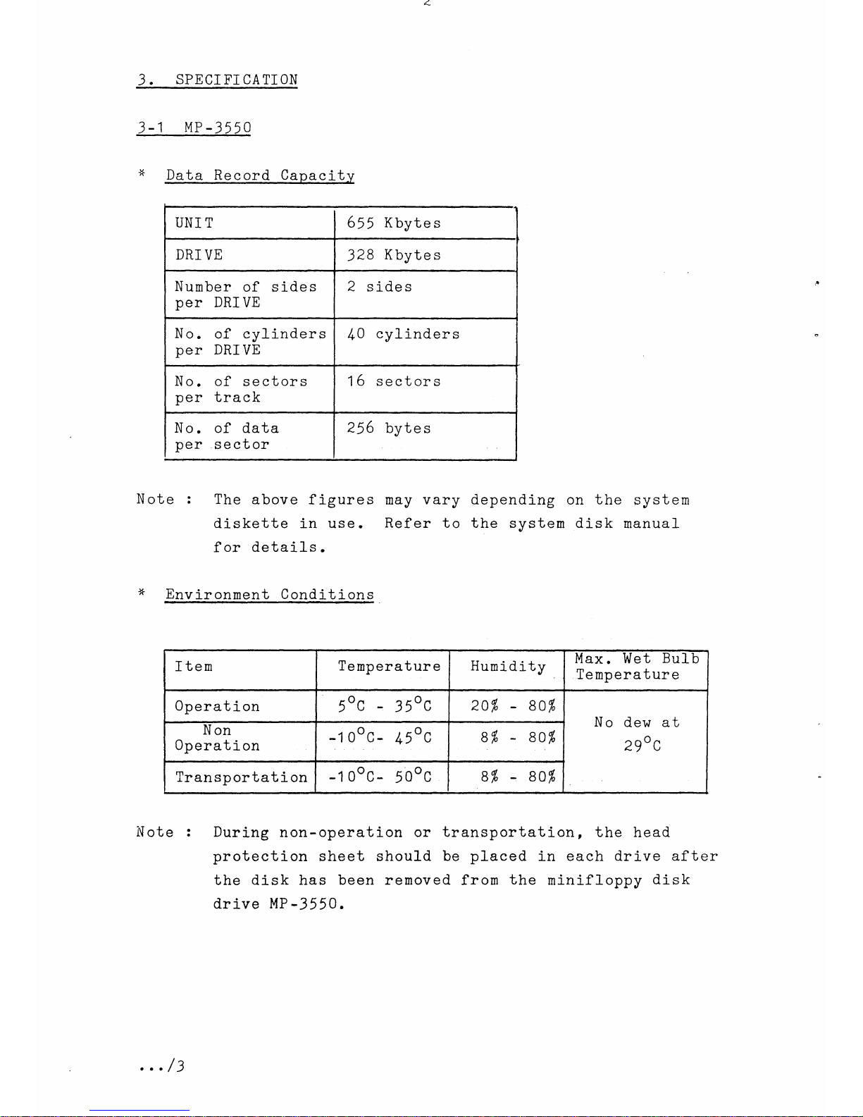
3.
SPECIFICATION
3
-1
tlP
-3550
x
Data
Record Capacitv
UNI T 655 Kbytes
DRI
VE
328
Kbyte
s
Number
of sides
per
DRI VE
2
sides
No.
of cyfinders
per
DRI
VE
/+0
cylinders
No. of
sectors
per track
16 sectors
No. of data
per
sector
256
bytes
Note
:
The
above figures
may
vary depending
on
the
system
diskette
in
use.
Refer to the
system
disk
nanual
f
or details.
*
Environnent
Conditions
ftem
Te
mp erat ur e
Humidity
Max.
Wet
Bulb
Temperature
0perati-on
5oc - 35oc
2or"
gof,
No
dew at
zgo c
Non
0perati
on
-1ooc-
/r5oc
B
1[
8oi[
Tran
sp or tat i on
-1ooc-
5ooc
B% - B0%
Note
:
During
non-operation
or
transportation,
the
head
protection
sheet should
be
placed
in
eaeh drive
afte
the disk has been
removed
from
the
minifloppy
disk
drive
MP
-
3550
.
. . .
/3
Page 6
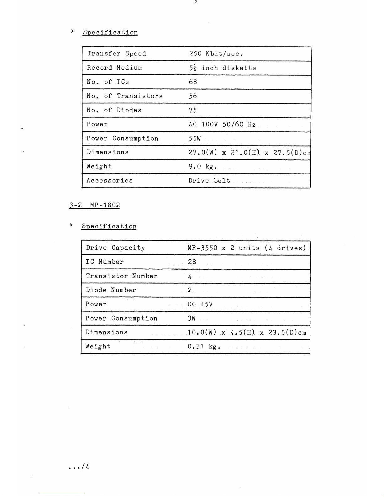
*
Specification
3
-2
t4P
-1
802
*
Spe
cifieation
Transfer
Speed 250
Kbi
L
f
sec
.
Record
Medium
5i
inch diskette
No.
of ICs
6e
No.
of
Transistors
56
No
.
of
Diode
s
75
P
ower
AC
100V
50/60
Hz
Power
Consumption
55W
Dimensions
27.0(W)
x
21
.O(H)
x
27.5(D)cn
We
ight
9.
o
kg.
Accessories
Dr:ive
belt
Drive
Capacity
MP-3550 x 2
units
(lr
drives)
I C Number
28
Transistor Number
lr
Diode Nunber
2
P ower
DC
+5V
Power Consumption
3W
Dirnens
ions
,1.0.0(W)
x
tr.5(jf-)
,x
23.5(D)
cm
We ight 0.31
kg.
.../4.
Page 7
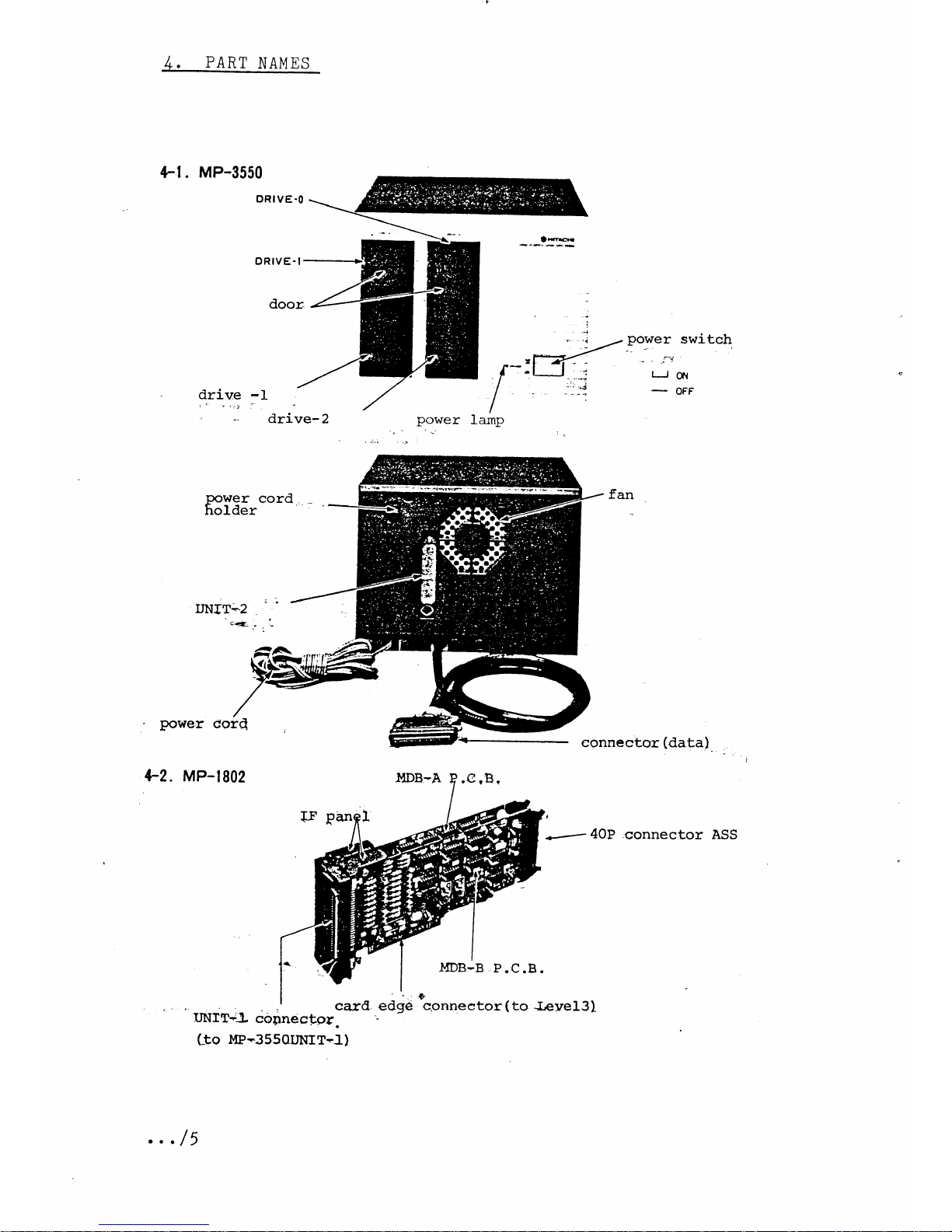
4.
PART
NAI'IES
4-l
.
MP-3550
oRrvE-0
ORIVE.I
drive
-1
drive-
2
power
switch
I roll
_
oFF
power
cord.
holder
fan
connector
(data)
POwer
Ccrrc
+-2. MP-|802
(-to
MP-355OttNIT-l)
l{DB-A
,C,8,
-I{DB-B
P.C.B.
-
'.-3
edge
conneetor
(to
J.eyel3)
power
lamp
.../5
Page 8
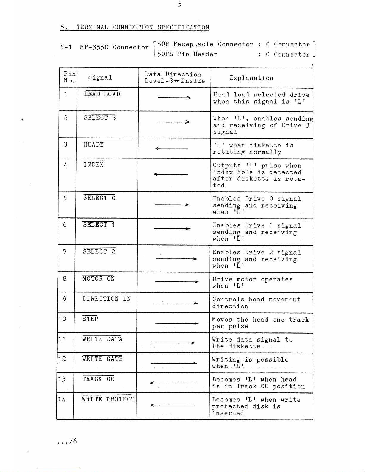
5-1
Mp-
3550
connector
Ilor
Receptac]-e
connector
: c connector
I
I
L
50PL
Pin Header
:
C Connector
J
q
/
5.
TERMINAL
CONNECTTON SPECTFI
CATI..ON
Pin
No.
S
ignal
Data
Direction
Level-3c'
Inside
Expl-anati
on
1
HEAD
LOAD
Head
l-oad selected
drive
when
this signal
is
tL
I
2 SE_IEET-3
___-__--_->
When
rL |
,
enables
sendin5
and
receiving
of
Drive
3
s ignal
3
ET.DY
rL I
when diskette
i-s
rotating
normally
/,
INDEX
<-
Outputs
rLf
pulse
when
index hole
is
detected
after
diskette
is rota-
ted
5
m0
Enables
Drive
0
signal
sending
and
receiving
when
lL I
6 SIET1
------=-+
Enables
Drive
1
signal
sending and
receivi-ns
when
lL I
7
mffi
Enables
Dri've
2
signal
sending
and receiving
when
lL I
8
MOTOR
ON
Drive
motor operates
when
lL I
9
DI
RECTI
ON
IN
Control-s
head
movement
direction
10 S
TEP
t
+
Moves
the
head
one track
per
pulse
11 i[mTETlm
Write
data signal to
the
diskette
12
WRI
TE
GATE
Writing
is
possibl-e
when
tL t
13
TRACK
OO
Becomes
tL
t
when head
is
in
Track 00
position
1l+
WRI
TE
PROTECT
Becones
rL
q
when
write
protected
disk is
inser:ted
...
/6
Page 9
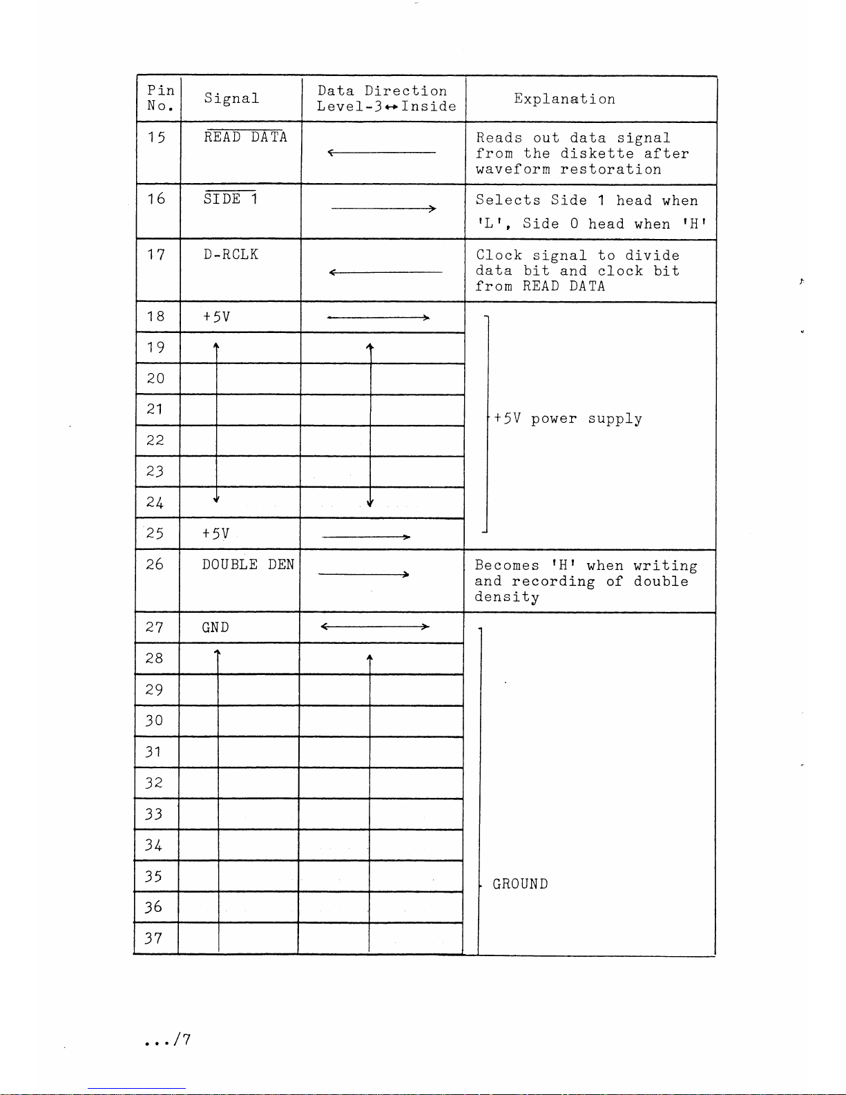
Pin
No.
S
i
gnal
Data Direction
Level-3**Inside
Explanati
on
15
READ DATA
Reads
out
data s ignal
from
the
diskette after
waveform restoration
16 mE1
Sel-ects
Side
t head
when
tLt
,
Side
0
head when
tH
t
17
D-RCLK
Clock
signal to divide
data
bit
and clock bit
from
READ DATA
1B
+5v
+
5V
power
supply
19
T t
20
21
zz
23
2/,1
J
J
25
+
5v
26
DOUBLE DEN
Becomes
rHr
when writing
and
recording
of double
dens
ity
27
GND
GROUN
D
2B
1 i
2g
30
31
)1
33
3lr
35
36
37
., . /7
Page 10
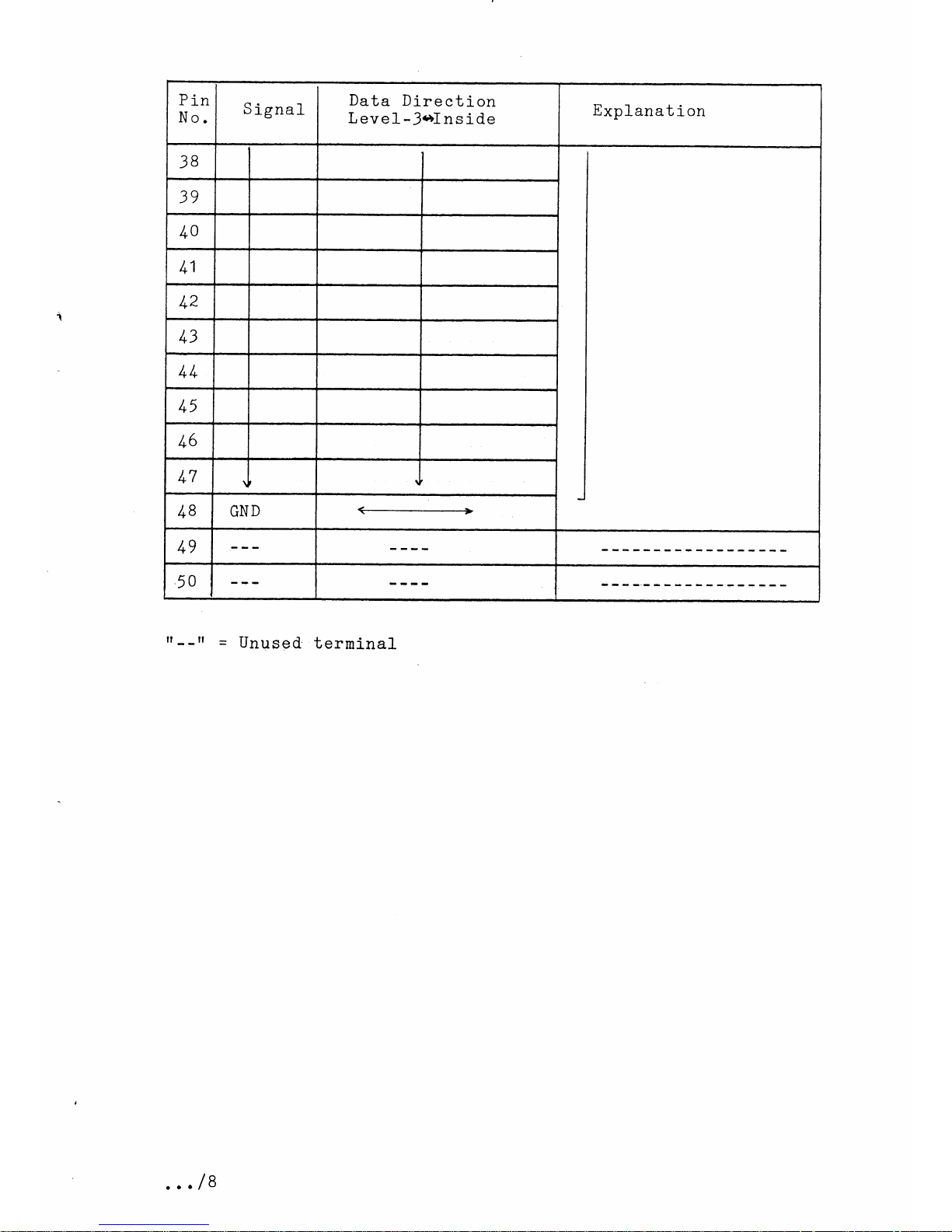
Pin
No.
S
igna 1
Data
Direction
Level-3oInside
E*planation
38
39
lr0
/+1
/+2
lr3
/+ lt
lr5
lr6
/+7
J
I
l+8
GND
lr9
50
rr--fr
=
Unused
termi-nal
.../8
Page 11
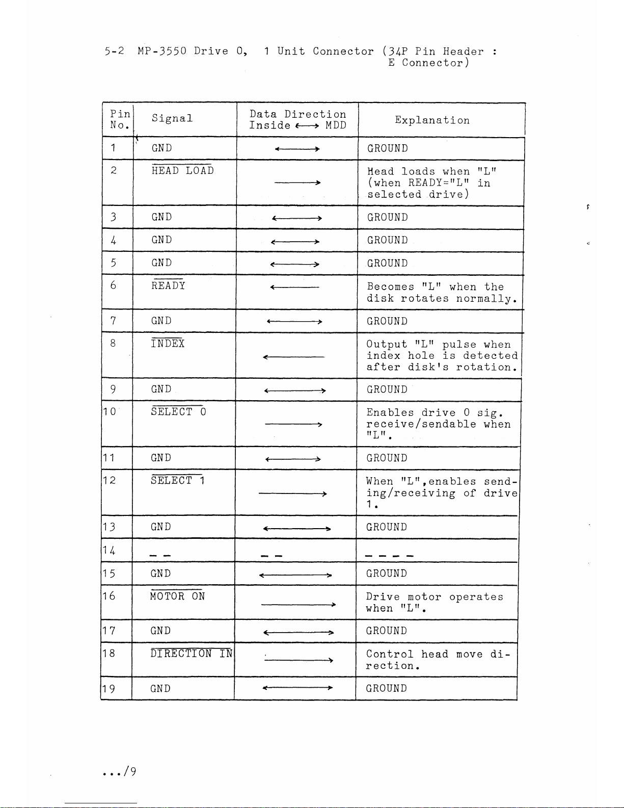
5
-2
MP
-
3550
Drive
0,
1
Unit
Connector
(l
tp
P
in
Header
:
E
Connector
)
Pin
No.
S
ignal
Data
Direction
fnside
H
MDD
Explanation
1
GND
GRO
UN D
z
HEAD
LOAD
-
Head loads
when
rrLrf
(
when
REA
DY
-
rr L tf
in
selected
drive)
1
GND
GRO
UN D
l
4
GND
<---.-->
GRO
UN D
5
GND
GRO
UN
D
6
nnalv
Becomes
rrLrr
when
the
disk rotates norma11y.
7
nnTn
LJII
]J
GROUND
B
INDEX
0utput
tfLrr
pulse
when
i-ndex hole is detected
after
diskrs
rotation.
GND +-+
GRO
UN D
10
Sgi,gCT
O
Enables
drive
0
sig.
receive/sendable
when
Itr
rl
!1
.
11
GND
GRO
UN D
12
SEIEMl
When
rfL
rr
,
enable s s end-
ing
frecei-ving
of
drive
1.
13 GND
GROUN
D
4t
t4
t\
GND GROUND
to
MOTOR
ON
Drive
motor
oDerate
s
when
lf
L
lf
.
17
GND
GRO
UN D
18
m Control
head
move
di-
rection.
1g
GND
GRO
UN D
...
/g
Page 12
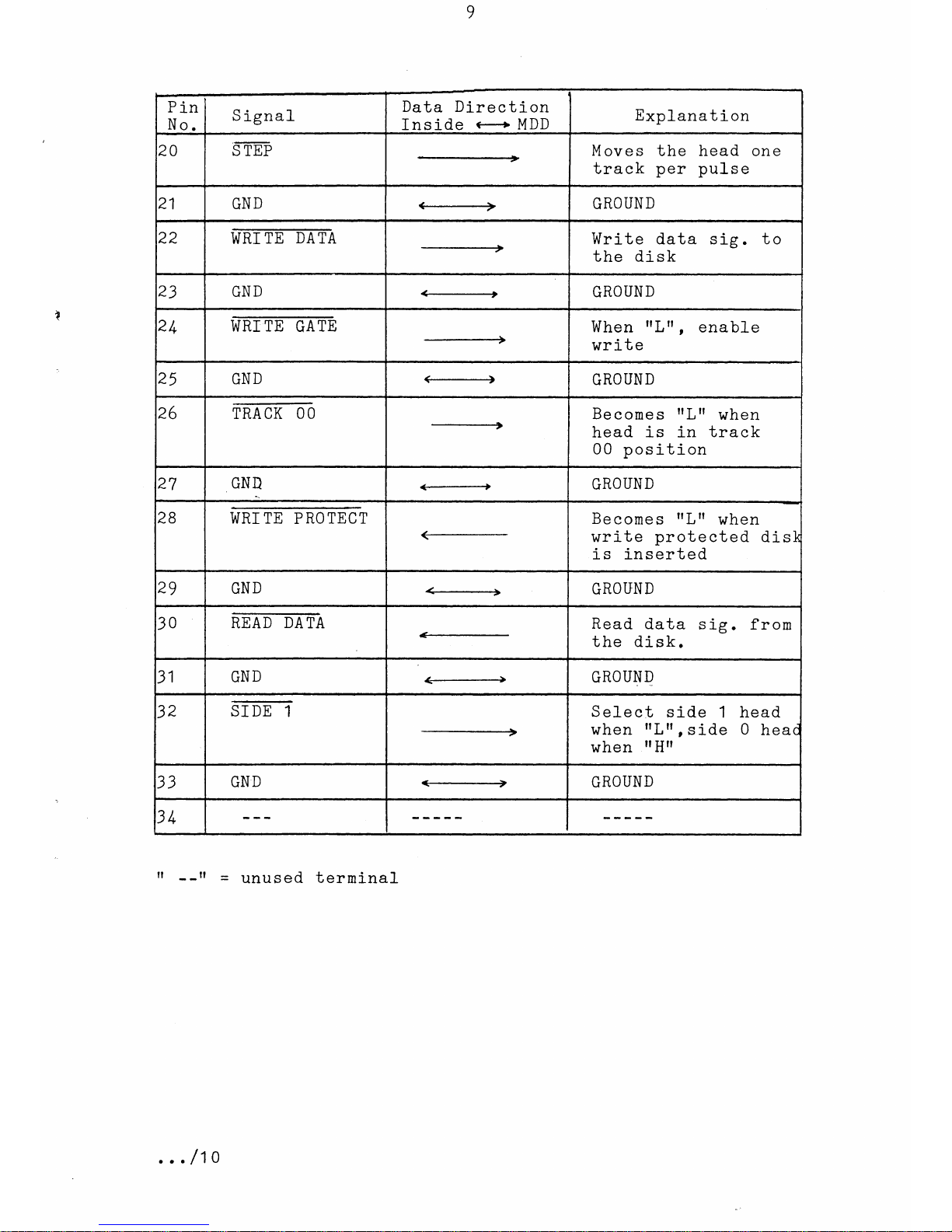
Pin
No.
S
ignal
Data Direction
Inside
c+
MDD
Explanation
20 s-m Moves the head one
track
per pulse
21
GND <-----€
GROUND
22
WRI
TE
DATA
Write data sig. to
the
disk
23
GND
4
GROUND
2/+
WRT
TE
GATE When
frLrr,
enable
write
25
GND
c---------)
GRO
UN D
26 TRACK OO
-------'
Be
c
ome s
fr L rf
when
head
is in
track
00 position
27
cNl
GROUND
2B WRI TE
PROTECT Beeomes
lrLll
when
write
protected
disl
is inserted
2g
GND
-
GROUND
30
READ
DATA
Read
data
s ig . from
the di-sk.
31
GND
<__--------)
GROUND
32
SI
DE.T
Seleet
side
t head
when
frLrtrside
0
heac
when
fr
Hil
33
GND
<___--+
GROUND
3lr
tr
--rr
=
unused
terminal
...
/10
Page 13
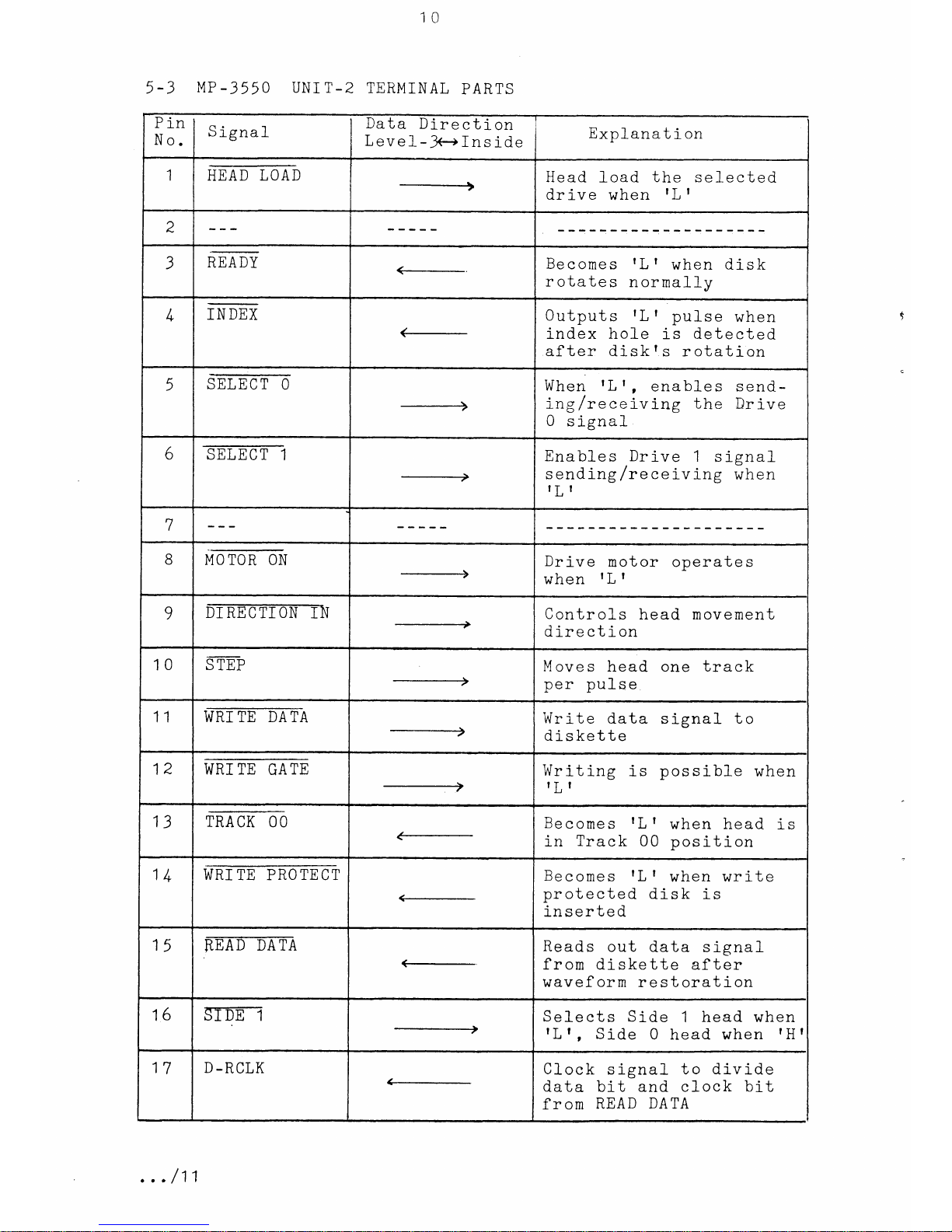
ItJ
5
-3
MP
-
3550
UNI T-2
TERMINAL
PARTS
Pin
No.
S
ignal
Data
Direction
Level-3<+fnside
Exnlanat
i
on
a
I
HEAD
LOAD
Head
load
the
selected
drive when
rL
I
I
3
REA DY
Becomes
rL
I
when disk
rotates
normally
lr
INDEX
0utputs
rL I
pulse
when
index hole
is
detected
af ter disk
I
s rotati-on
5
SELEcro
When
tL t,
enables send-
itg
f
receiving the
Drive
0
s ignal
6
SELECT
1
--?
Enables Drive
1
signal
s end
ing f r e ce
iv ing
ih"rt
lT I
7
tuoton oll
--->
Drive
motor operate s
when
lL I
9
m
Controls
head movement
direction
10
d mnn
\IHP
V
LJ-IL
M
ove
s head
one track
per puls
e
11
WRI TE DATA
----)
Wr
ite
data
s
ignal
t
o
diskette
12
WRI
TE
GATE
--_-J
Writing
is possible
when
rL
r
13
TRA
CI{ O O
Becomes
rL
I
when head
is
in
Track 00
Dosition
1/+
WRI
TE PROTECT
Becomes
rL
I
when write
protected
disk is
inserted
15
mmIn
F--
Reads
out
data s ignal
from diskette
after
waveform restoration
16
STIE-]
--)
Selects Side'1
head when
rL |
,
Side
0
head
when
rH
t
17
D-RCLK
Cl-ock
signal
to divide
data bit and clock
bit
from
READ DATA
...
/11
Page 14
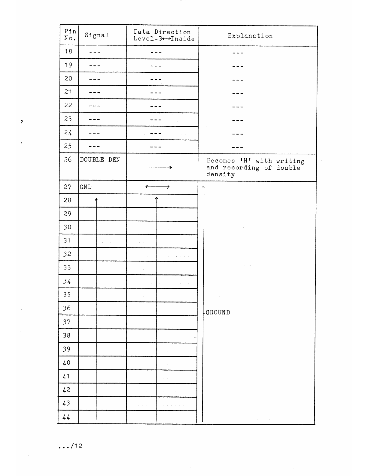
Pin
No.
S
ignal
Data
Direction
Level-3<--.+lnside
Explanation
1B
1g
20
21
22
23
2/+
25
26 DOUBLE
DEN
_-....--
Becomes
fH I
with
writing
and
recording
of
double
dens
ity
27
GND
GROUND
2B
1
2g
30
31
32
33
3L
35
36
37
3B
39
/+0
l+1
l+2
lr3
/, lr
,
.
.
/12
Page 15
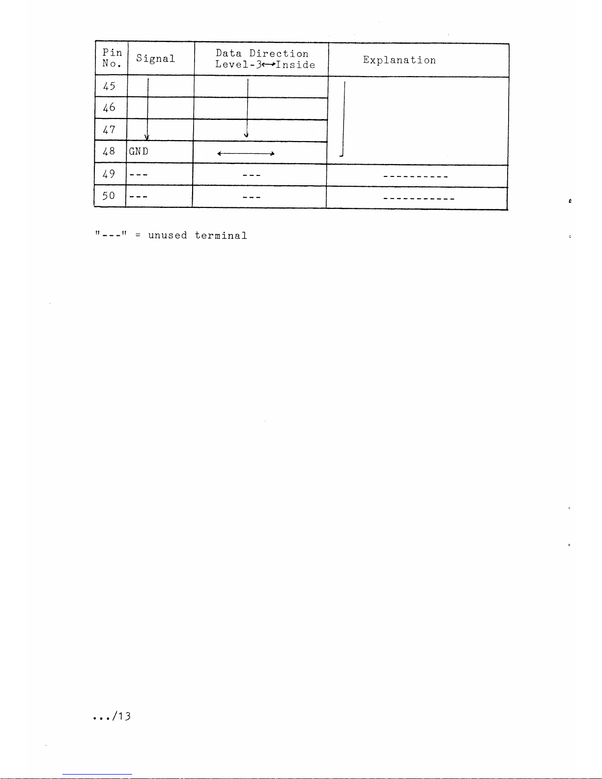
Pin
No,
S
ignal
Data
Direction
Level-3e'-Inside
E*planat
i on
lr5
/r6
t7t
4l
J
/+8
GND
).4
.+/
50
fr---rt
=
unused
terminal
...
/13
Page 16
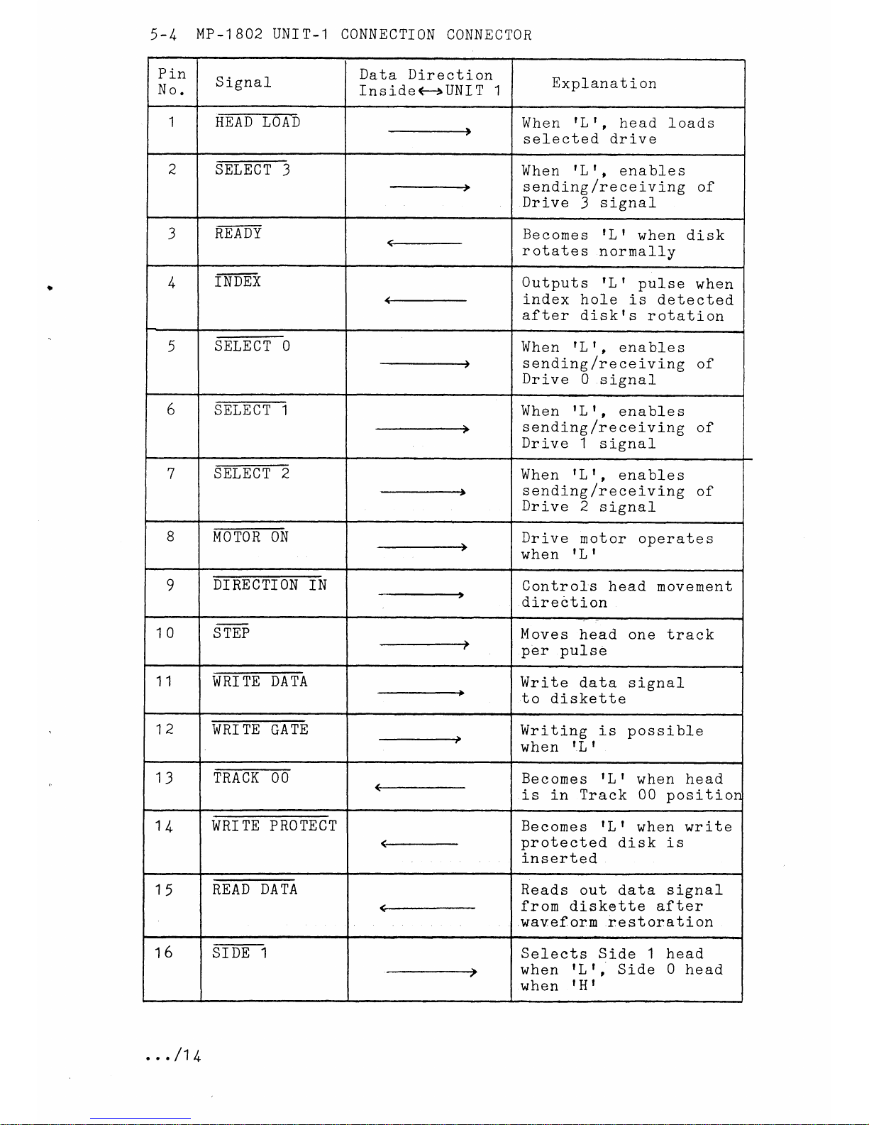
5.1
MP-1 BO2 UNI
T.1 CONNECTION
CONNECTOR
Pin
No.
S
ignal
Data Direction
Ins
ide G+UNI T 1
Exol-anation
I
fi]il[D-ImD
When
rL
t,
head loads
selected drive
2 SELECT
3
When
tLt,
enables
sending
freceiving
of
Drive
3
signal
3
MTffi
Becomes
rL
I
when
disk
r
otate
s
normally
/+
rm-ET Outputs
rL I
pulse
when
index
hole
is
dete
cted
after
diskfs rotation
(
ffio
---.9
When
tLr,
enables
sending
freceiving
of
Drive
0
s
ignal
6 SELECT
1
When
tLt,
enables
sending
/"uceiving
of
Drive
1
signal
7
sj;Em
When
rLr,
enables
sending
f
receiving
of
Drive
2
signal
B
MOTOR ON
Drive
motor
oDerate
s
when
rL I
9
DI
RECTION
IN
Contr
ols
head movement
direction
10 S TEP
Moves
head
one track
per pulse
11 WRI
TE
DATA
Write
data signal
to
diskette
12
WRI
TE
GATE
Writing
is
possible
when
rL I
13
TRACI{O6'
Becomes
rL
I
when head
is
in
Track 00 positior
1/+
WRI
TE
PRO
TECT
(-
Becomes
rL
I
when write
protected
disk is
inserted
15
READ
DATA
a-
Reads
out
data
signal
from diskette
after
waveform restoration
16
SIDE
1
.--=+
Selects
Side
t head
when
tLr,
Side
0
head
when
rHr
.
. .
/1/n
Page 17
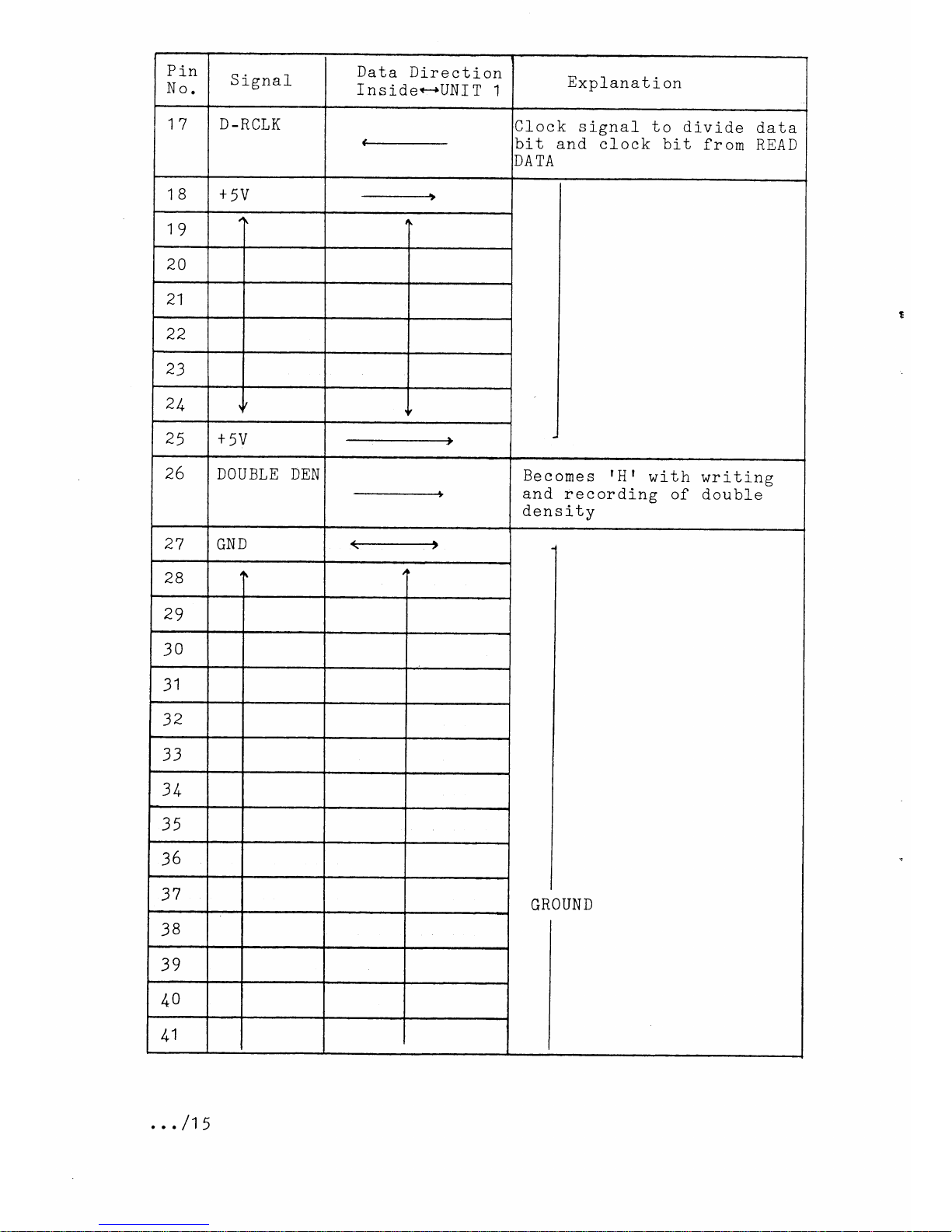
Pin
No.
S
igna
1
Data
Direction
f nside.*UNI
T
1
Explanation
17
D-RCLK
Clock
signal
to divide
data
bit and
clock bit
from
READ
DA
TA
18
+5v
1g
t
I
20
21
22
23
2/+
I
I
25
+5v
26
DOUBLE
DEN
Becomes
rHr
with
writing
and
recording
of
double
dens
ity
27
GND
-
GROUND
28
I
2g
30
31
32
33
3lr
35
36
37
38
39
/+0
/,r1
.../15
Page 18
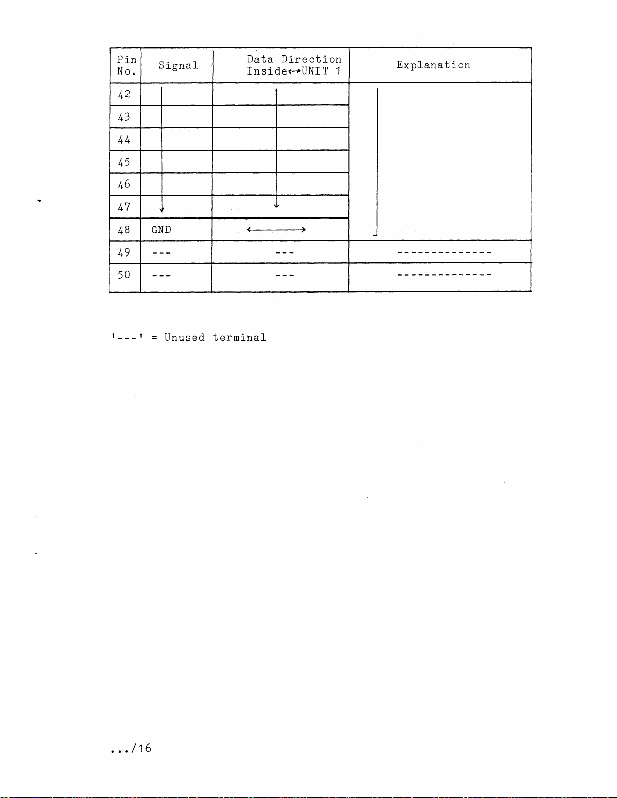
Pin
No.
S
ignal
Data
Direction
Inside*+UNI T 1
Explanat
i
on
/+2
/r3
/,
lr
lr5
/+6
/+7
I
I
/+8
GND
/-9
50
l---l
=
Unused terminal
.../16
Page 19
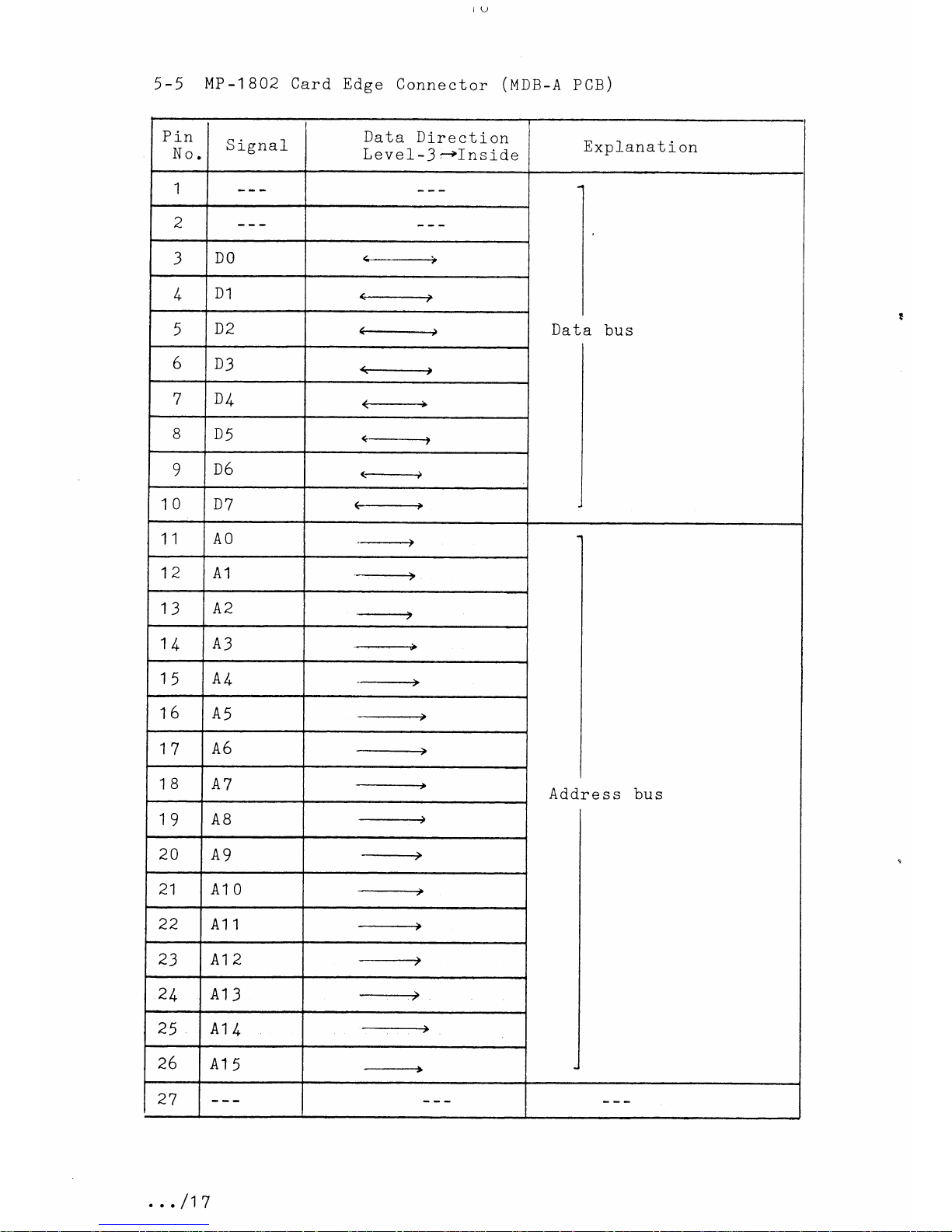
5-5
MP-1802 Card
Edge
Connector
(Unn-A
PCB)
Pin
No.
S
ignal
Data
Directi-on
Level-3;Inside
E"planation
1
Data
bus
2
3
DO
lr
D1
5
D2
(-j
6
D3
7
D/+
<--+
8
D5
c--__J
9
D6
(-________)
10
D7 e------------?
11
AO
.-__)
Addre
s s
bus
12
A1
--.....=-)
13
A2
--
1/+
A3
15
A/+
16
A5
17
A6
18
A7
1g
A8
----=+
20
A9
21 A1 0
--_---+
22
A11
---+
23 A1 2
2lr
A1
3
25
A1 /+
:--::--)
26
A1
5
-----------+
27
.
..
/
j7
Page 20
Page 21
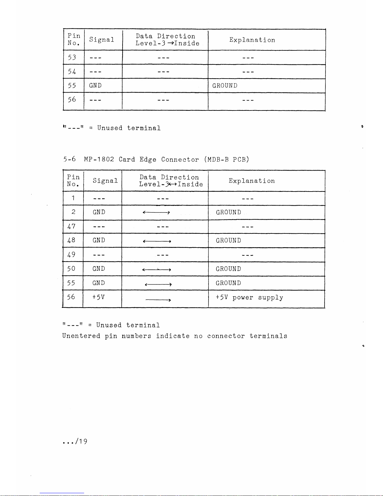
Pin
No.
S
ignal
Data
Direction
Level-3
-+Inside
Explanat
i
on
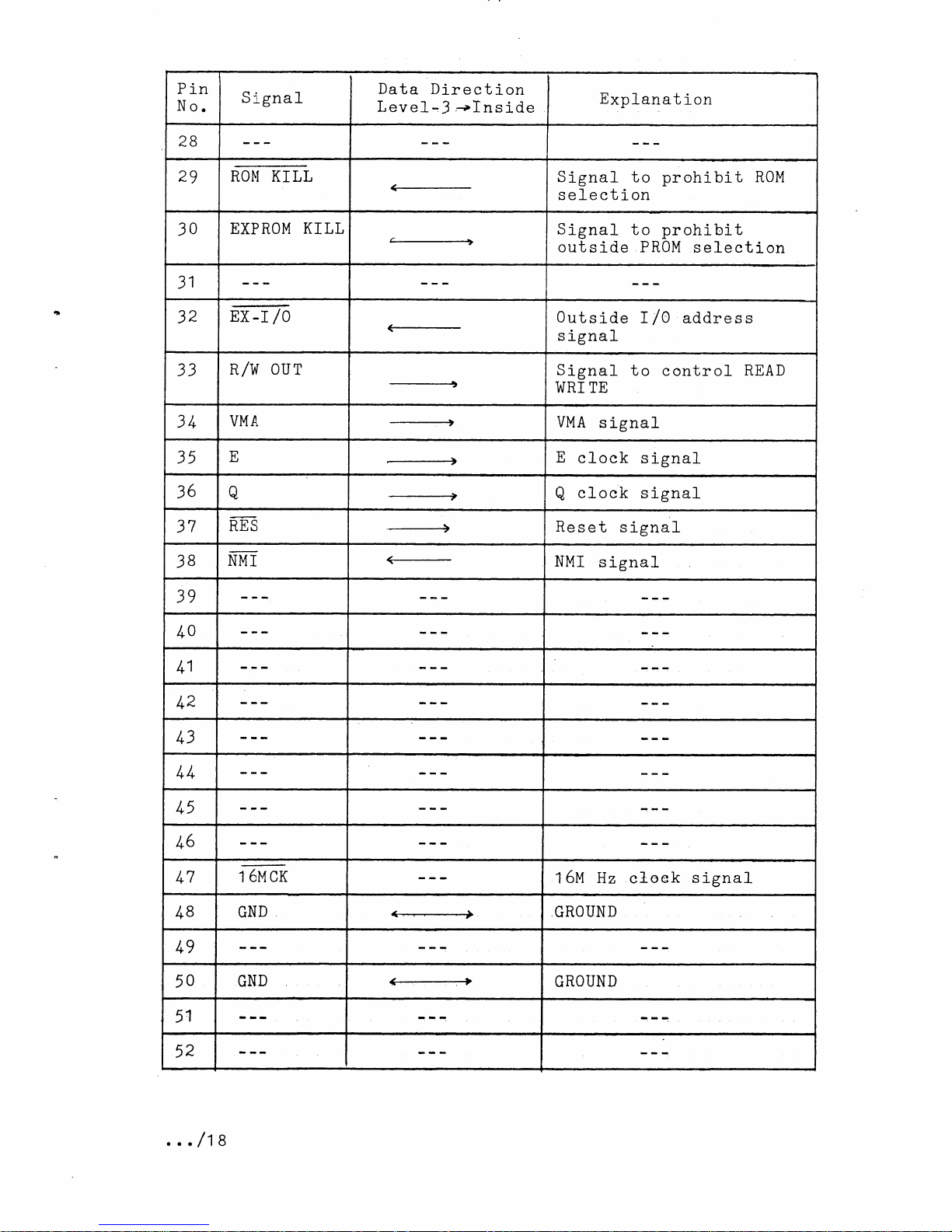
53
5/r
55
rl T\T T\
UNU
GRO
UN
D
)o
rr---rr
=
Unused
terminal
5-6
MP-1802
Card
Edge Connector
(t'lle-n
PCB)
fr---tf
=
Unused
terminal
Unentered
pin
numbers indicate no
connector terminals
Pin
It
II
\J.
S
ignal
Data Direction
Level--.lr.-.Tnside
Explanat
i
on
1
2
rtTTN
\TII
IJ
<____t
GROUN
D
/r7
/+B
GND
<----
GROUN
D
lr9
50
GND
(---€
GROUN
D
55
GND
GROUN
D
56
+5V +
5V
power
supply
...
/19
Page 22
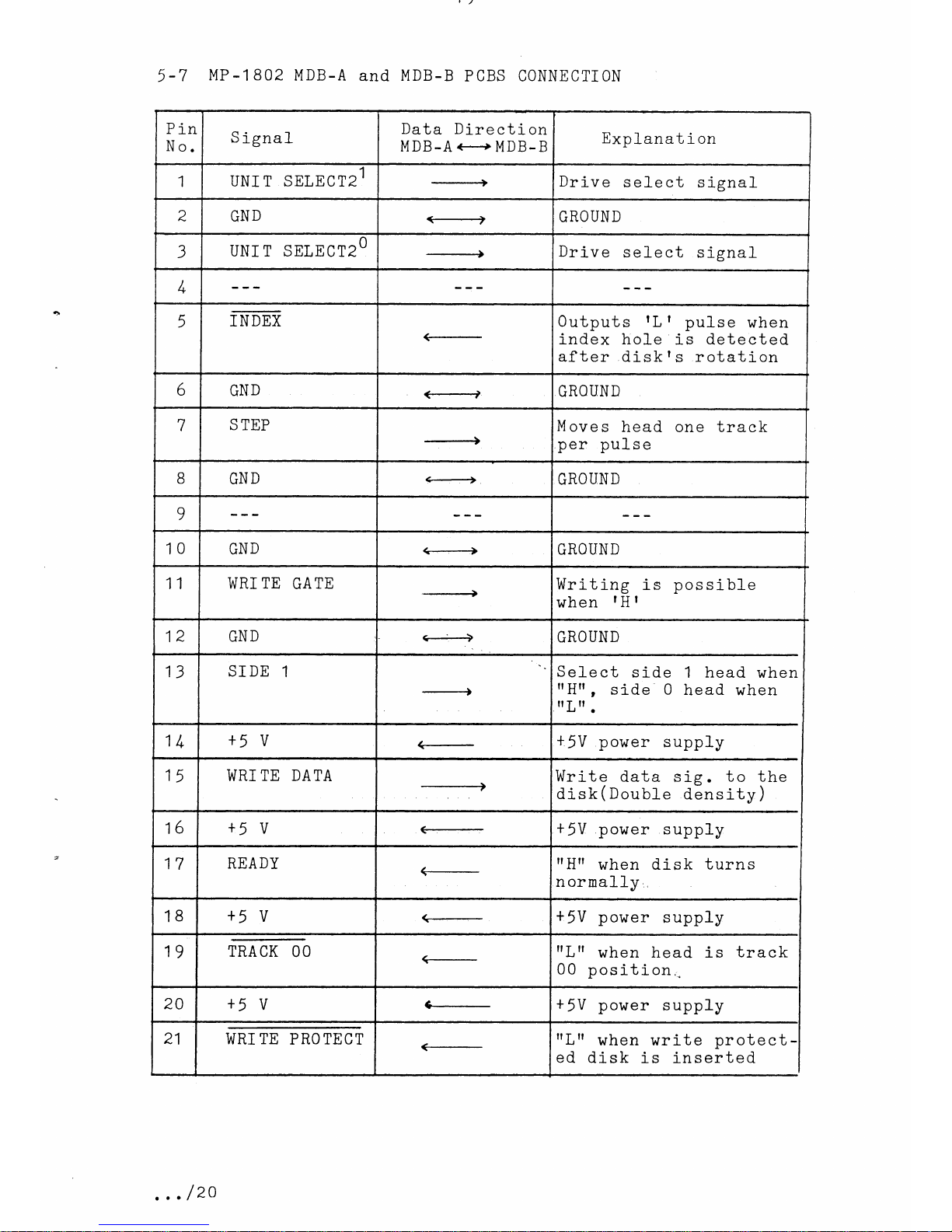
5-7
MP-1802
MDB-A
and
MDB-B
PCBS
CONNECTI0N
Pin
No.
S
ignal
Data
Dire
cti
on
MDB-A
e+
MDB-B
Exol-anat
i on
1
I
UNI T SELE CT21
-----------+
Drive
select
signal
GND
GROUND
3
UNI T SELECT2O
--+
Drive
select
signal
/r
5
INDEX
Outputs
rL t
pulse
when
index hole
is detected
after
diskIs rotation
6
GND
<--
GROUN
D
7
S
TEP
-+
Moves
head one track
per
pulse
8
GND
#
GROUND
9
10 GND <--:-+
GROUND
11
WRI
TE
GATE
Writing
is possible
when
lHf
12
GND
<-+
GROUND
13
SIDE
1
+
Select
side t head
when
rrHfr,
side
0
head when
ilLft.
1/+
+5
V
<-
+
5V
power
supply
15
WRI
TE DATA
Write
data
sie.
to the
disk(Double
d6nsity)
16
+5
V
€-
+5V
power
supply
17
READY
(-
trHfr
when disk
turns
I
normally
I
18
+5
V
+
5V
power
supply
1g
rna clr o o
<-
rrLrr
when head is
track
00
position,..
20
+5
V
6_ +
5V
power
supply
21
WRI
TE
PROTECT
(-
rrLrf
when wri-te
protect-
ed
disk is inserted
.
..
/20
Page 23
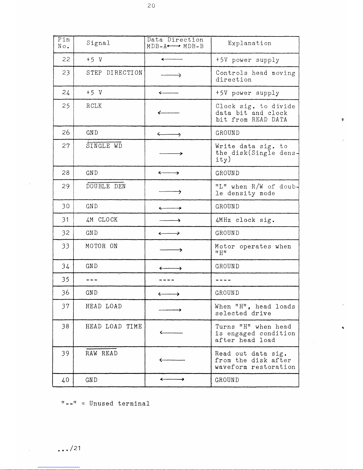
)el
Pin
No.
S
ignal
Data Direction
MDB-Ae
MDB-B
Ex'olanation
22
+5
v
<-
+
5V
power supply
STEP
DIRECTION
t
Controls
head moving
direction
24
+5
v
<-
+
5V
power supply
25
R
CLK
Clock
sig.
to
divide
data bit and clock
bit
from
READ
DATA
26
GND
+--)
GROUN
D
27
SINGLE
WD
Write
data
sig.
to
the
disk
(
Single
d ens
-
ity
)
28
GND
GRO
UN
D
2g DOUBLE DEN
rrLrt
when
R/W
of doub-
Ie density mode
30
GND
€--------)
GROUN
D
31
LI,I
CLO CK
$rlHz
clock
sig.
Jz
GND <-----+
GRO
UN D
33
MOTOR
ON
M
of or
operate
s
when
rr
Hrl
3/,
GND
GROUN D
?(
36
GND
(------)
GROUN
D
37
HEAD LOAD
F_-----)
When
frHrr
,
head loads
seLected dri-ve
38
HEAD LOAD TIME Turns
rr
Hrf
when head
is
engaged condition
after:
head load
39
RAW READ
Read
out
data
s ig
.
from the
disk
after
waveform restoration
/,r0
GND
<-=+
GROUND
rr
- -rf
-
Unused
termi-nal
...
/21
Page 24
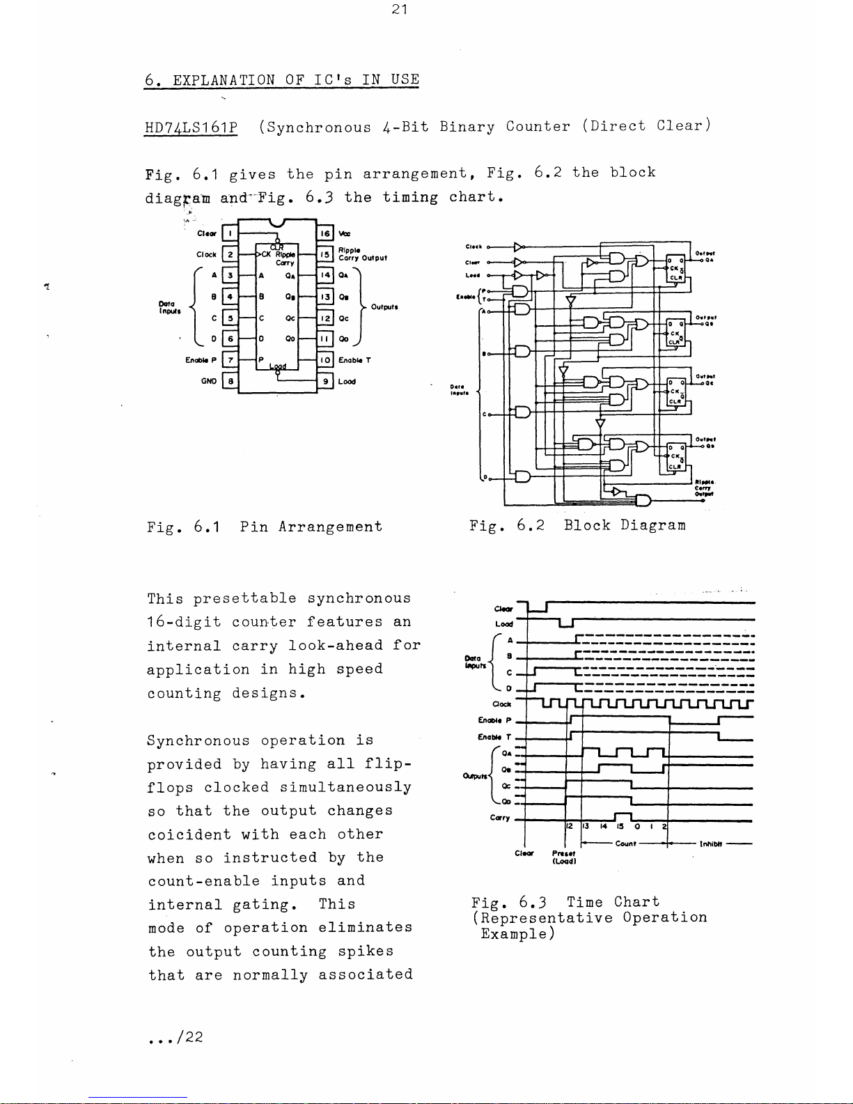
21
HD7 /+LS1
61P
(Synchronous
4-Bit
Binary
Counter
(lirect
Clear
)
Fig
. 6 ,1
give s
the
pin arrangement
,
Fig
.
6.2
the block
diagpan
and"-Fig
.
6
,3
the t iming
ehart
.
Fig
.
6.1
Pin
Arrangement
Fig.
6.2
Block
Diagram
;,.
Corrt
Oufpul
o^)
I
o.
l
>
Oureufr
ocl
u)
.:.'
,j.
'
Ct.o.
Cl o€L
(A
I
I
l8
m&. {
lc
I
'\0
Endb P
GNO
This
presettabl-e synchronous
16-digit counter
features
an
internal
earry
look-ahead
for
applieati-on
in high speed
counting
designs.
Syrchronous
operation
is
provided
by having
all flip-
flops
clocked
s imultaneously
so
that
the
output changes
coicident
with
each other
when
so
instructed
by
the
c ount
-
enabl-e
input s
and
internal-
gating.
Thj-s
mode
of
operation
elininates
the
output
counting spikes
that
are
normally
as s
oci-ated
Fie
.
6.3
Time Chart
(
n6presentative
Operation
Exarrple
)
k
Lood
(a
I
ooro )
s
t+utr)
lc
Lo
J1
€ncde t
(o^
I
lOr
o.rwn1
lft
Lo
Cary
Chc Pnrl
(t-oodl
.. . /22
Page 25
with asynchronous
(
ripple clock)
counters
.
A
buffered
clock
input
triggers
the
four flip-f1ops
on
the
rising
(positive-
going
)
edge of the
clock
lnput waveform.
This
counter
is f u11y progranmabl-e;
that
is,
the outputs
may
be
preset
to
either
I
H
I
and
rL I
level, As
presetting
is
synchronous,
setting
up
a l-ow level at
the
load input
disables
the
counter and causes
the
outputs to
agree
with
the
setup
data
after
the
next
cl-ock
pulse
regardl-ess
of the
levels
of
the enable
inputs. Low-to-high
transiti-ons
at
the
load
input
should
be
avoided
when the clock
is lor^r
if
the
enable inputs
are
high at or before
the
transition.
The
clear
function
is asynehronous
and a
low l-evel
at the clear
input
sets all
four of
the
flip-flop
outputs
low
regardless
of
the
levels
of
c1ock, load, or
enable
input s
.
The
carry
look-ahead
circuitry
provides
for
cascading
counters
for n-bit synchronous
appl-ications
without
additional
gating.
f nstrumental
in
accomplishing this
function
are
two
count-enable
inputs
and
a
ripple
earry
output.
Both
c ount - enabl-e
input s
(p
and
T
)
must
be
high
to
count,
and
input
T
is fed
forward
to
enable
the ripple carry
output. The
ripple carry
output thus
enabled
wil-l
pr oduce
high vel output
puls
e
with a duration
approximately
equal to
the high-level portion
of the
QA
output,
This
high-level
overflow
ripple
carry
pulse
can be
used to
enable
successive
cascaded
stages. High-to-1ow
1evel
trans-
itions
at
the
enable P
or T inputs should
occur onlv
when
the
clock
input is high.
I4C/+0.2/+P
(
Dual
Voltage-Controlled
Mu1ti-Vibrator)
vcc
I
oc
--t-J
Gt{o
I
orr?
I
Cnlrolt
C
r
t
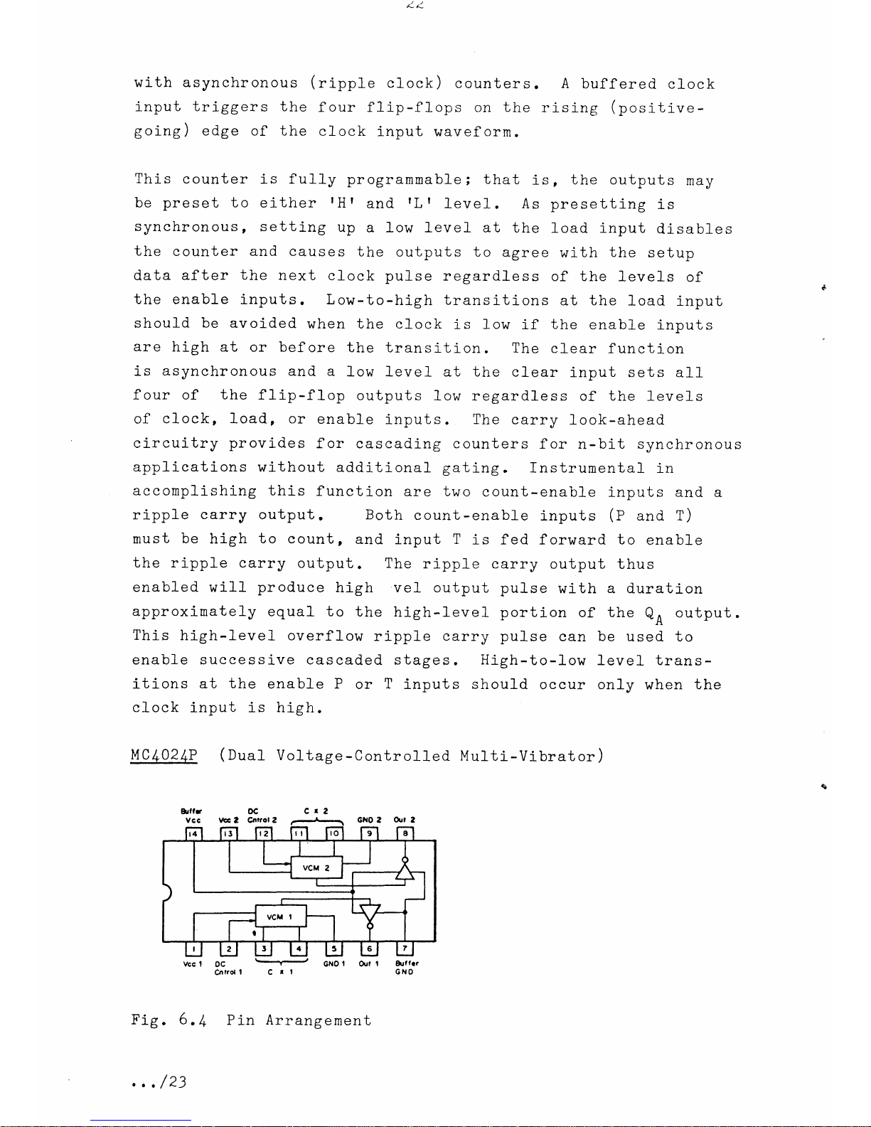
Fig. 6./,,
,
,
,
/23
&rf
lrr
G
r{0
Pin
Arrangement
Page 26

Fig
'
6
'
/n
shows
the
pin
arrangement.
This
is
two
vcMs
(voltage-
controlled
multi-vibrators
)
with
output
buffer,
The
oseillating
frequency
is
controlled
by
the
DC
voltage
applied
to
the
DC
control-
terminal
and.
is
used
f
or
the
pLL
(phase
Locked
Loop
)
in
digital-
ci-rcuit
wlth
the
phase
Detector
(uc4a/n/).
I,ICl,0L/r!
(phase
Detector)
Rcf
crcnco
oorn I vdiobla
Llg
tn up
ort
oorn
2 Gt{o
Fig
.
6,5
Pin
Arrangement
Oottr
9p5r
11raP
Vcc
Up
r
W
2
la
Ou||
t||
qJTruT
The
pin
arrangement
is
consists
of
two
phase
is
used
in
the
ptl
in
(uc
402
/+p
)
.
given
above
in
Fig
.
6.5
. The
I C
detectors,
a
eharge
purnp
and
AMp.
ft
digital-
circuit
together
with
the
vcM
Phase
Detector
#l
and
#z
are
used
when
the
input
signal
to
the
Variable
termi_nal
is
delayed
0o
and
90o
fron
the
input
signal
to
the
Reference
termi-nar.
(trre
input
signal
at#2
Reference
and.
variabre
terninars
must
have
501, duty.
)
It
outputs
a
pulse
(rr;96rr
which
corresponds
to
the
falling
edge
phases
input
The
charge
punp
D=tr1tt
and
U=ttLtt)
When
the
lnput
signal
phase
and
Variable
terminals,
the
i
mpedanc
e
.
(
fne
s
ignal
f1
ow
..,/2/,
active
)
to
the
Up,
Down
terminal_
difference
of
two
digital
signal
to
the
Reference,
Variable
terninals.
converts
the
phase
fast
or
delay
(respectivery
to
either
q9V
or
2.3V.
difference
is
0o
at
the
Reference
charge
pump
output
becomes
high
sets
Up1
(UpZ)
to Up
fN,
Downl
Rcfcrcnco
Oorn I Vdiobla
Page 27
(
Down2
)
to
Down
IN
and
Up OUT,
Down OUT
to
make AMP IN.
)
r1
l.
CI R
CUI T EXPLANA TI ON
7
-1
Structure
The
LeveL-3
minifloppy disk
system
consists
of the
minifloppy
disk unit
MP
-
3550
and the
minifloppy
disk
card MP
-1
802.
The
MDDs
(mini
disk drive
units),
a
power
unit and a
VFO
sep
ayator are i-ncorporated
in
the MP
-
3550.
The
MP-1802
includes
an
IC61
SFDC
(floppy
disk
controller)
and MDD
interf
ace
ci-rcuit,
an address
decoder circuit
and
MDD
select ci-rcuit among
others
.
f t transf
ers
the
interf
ace
signals
between the Lev
eI-3
and
minifloppy
disk
unit
MP
-
3550.
The
basic
drive software
is in
EPROM
(IC61
7)
on the MP
-1
802
and other
system software
is
on
the
0S
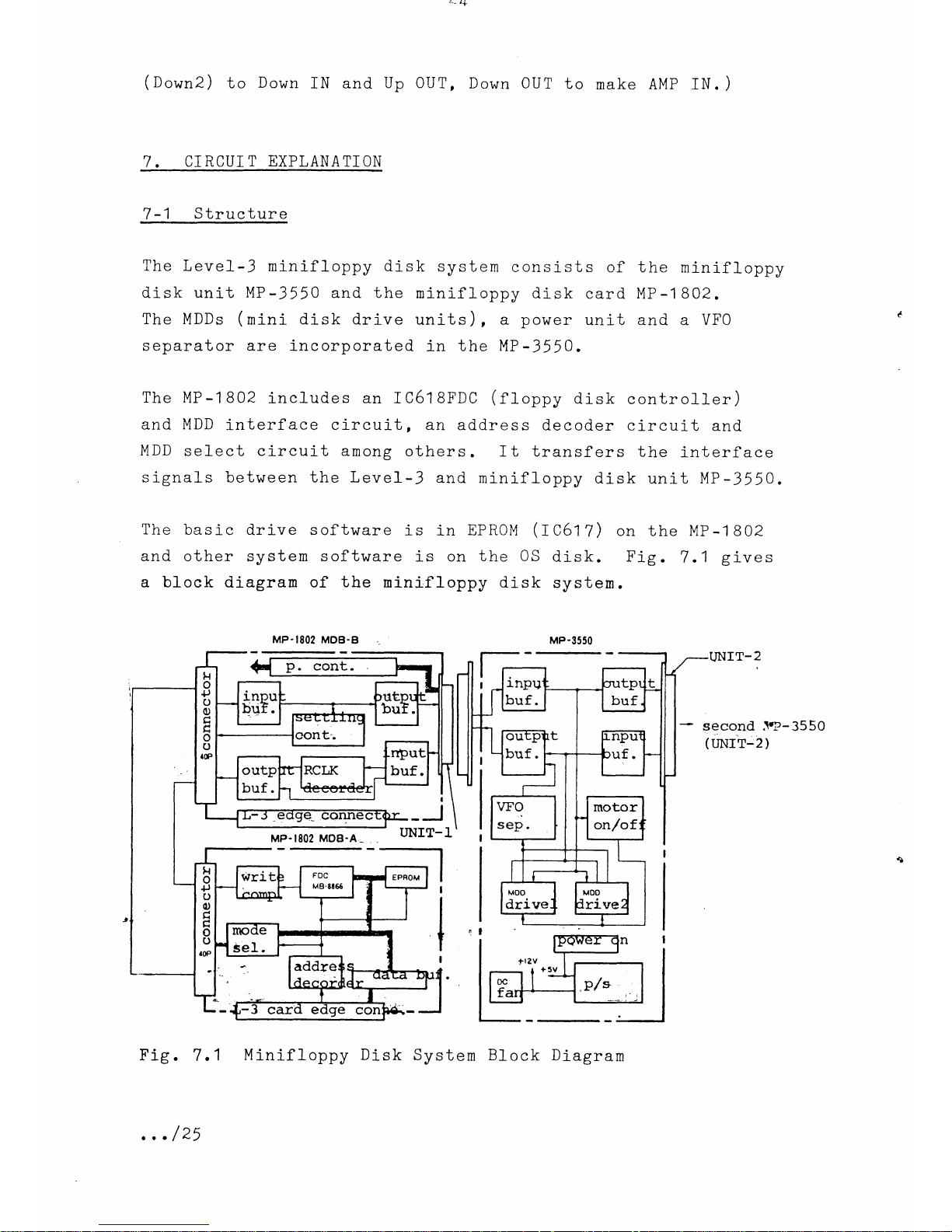
disk. Fig.
7.1
gives
a bl-ock
diagran
of the
ninif f oppy disk
system.
MP.I8O2
MOB-B
MP-3550
LINTT-2
sgcqnd .t?-
3550
(
uNrr-2
)
Fig.
7.1
I
-J
t{
o
+J
o
c)
tr
H
o
o
r0P
rnpu
buf.
tl
o
+)
o
o
c
q
o
(J
a0P
,
.
.
/25
Minifloppy
Disk
System Bl-ock
Diagram
Page 28
(1)
Recordins
Medium
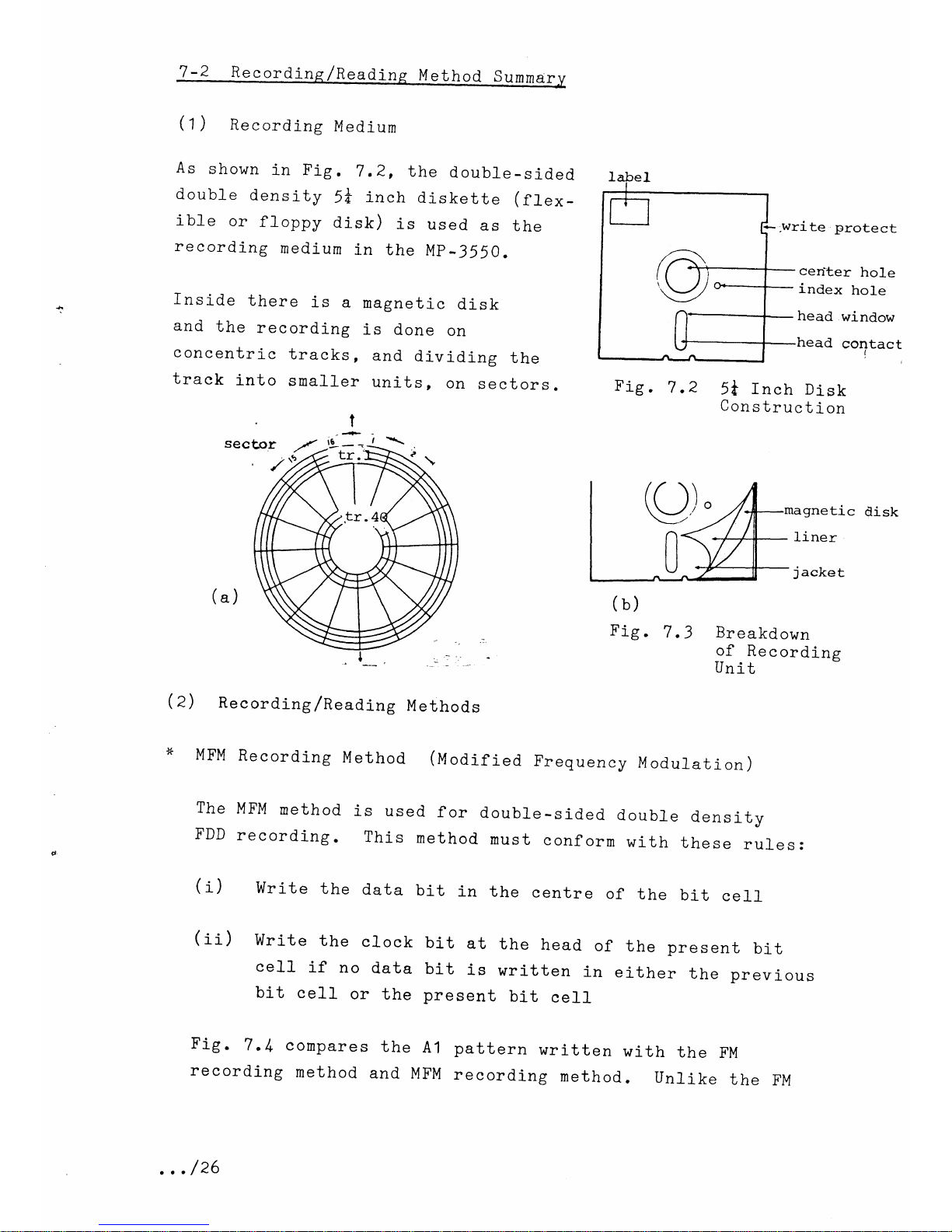
As
shown
in Fig
.
7.2, the
double_sided
double
density
5*
inch
diskette (fte*_
ible
or
floppy
disk)
is
used
as
the
recording
medium
in
the
li,lp
_
3550.
Inside
there
is
a
magnetic
disk
and
the
recording
is
done
on
concentric
tracks,
and
dividing
the
track
i-nto
snaller
units,
on
sectors.
sector
./,
'
,/t
(a)
Fig.7.2
(r)
Fig
.
7.3
5t
Inch
Disk
Construction
write
protect
center
hole
index
hole
head
window
head
coqtact
gnetic
disk
iner
acket
(2)
Recording/Readlng
MFM
Recording
Method
.-.
-
,
'
M
ethods
(uoaified
Frequency
Br
e
akd
own
of
Recording
Unit
Modul-ation)
(
i)
write
the
data
bit
in
the
centre
of
the
bit
cell
The
MFM
method
is
used
for
FDD
recording.
This
method
(ii)
Write
the
clock
cell
if
no
data
bit
celI
or
the
Fig
.
7
.
/,
compares
the
A1
reeording
method
and
MFM
double
-sided
d.oubl_e
dens
ity
must
conf
orm
with
these
rul_es:
bit
at
the
head
of
the
present
bit
bit
is
written
in
either
the
previous
pre
sent
bit
ee1l
pattern
written
with
the
FM
recordirg
method.
Unlike
the
FM
t
.
,
.
/26
Page 29

recording
method,
clock
bit does
not
the
self-clocking
VPO data sep arator
nethod.
bit
ce
bit
cell
26
with
the MFM
necessarily
method is not
i-s required
reeording method r &s the
have to
be in the bit cell,
possibl-e.
Theref
ore,
the
for
the
MFM
recording
)*
record
Fig.
J.4
Comparison
of the
A1
pattern
with
the FM
and
MFM
re c ording method
VFO
Data
Separator
VFO
is
an abbreviation
of Variable
Frequency 0scillator.
In the MFM
recording
method, it
becomes
impossible to
generate
the window
for
the
data bit
from
the clock bit.
VFO generates both
the
cl-ock
bit and
data
bit
window
correctly
even
if
there
is no clock
bit
in the read data
fr om the di
sk
.
The
structure of
the
VFO data
seDarator i s illustrated
in
Fig.
7.5.
read
data
sep.
data
sep.
clock
Fig.
'1
.5
filter
volta$e
...
/27
VFO
Data Separator
Structure
Exarnple
Page 30

r*
Read
Method Structure
When
the
disk is inserted in
the
MDD,
the magnetic
disk in
the
jacket
is
rotated
at a
constant
speed
by the
drive
motor.
The
head is
moved half
a
circle
by
the
stepping
motor and
the
track
position
and
sector
position
are
desi-gnated.
(Refer
Fig
. 7.9.)
Read
fwrtLe
to the magnetic
disk is effected
in
aecordance
with
the
magnetic flux change
in
the
head through
the
read/
write circuits
in
the
MDD.
(Refer
Fig.
7.6.)
inputinf,.
to
to
o
o 0l
write
data
0 o oDc0cocoola:ClOck
n n n n n fl\o:data
head
flux.rt"ffi
read,out
votr..W
differ.
outpuaff
comparater
output
read
data
M
outgutinf.
I
o
I
o
o o
ol
Flg.
7.6
Read
/llr:-t,e
with
MFM Recording
Method
(3)
Recording
Formatting
*
Track
Formatting
MP-3550
adopts
the
16 sector/track
fornatting
for
soft
sector track formatting.
As
shown
in
Fig
.
7.7,
the
beginning of the
track
is shown
by the
preamble
and
each
byte
number in
MFM
is
about double
that
of
FM.
The
data
in the
gap
is
(rr')rA
in
FM but
(rc),,
in
MFM.
..
.
/29
Page 31

secto
t
anble
*
..
has missing
clock
**
ID
field
***
cyclic redundancy
check
Fig
. 7
.7
Track Formatting
(27)
ro'
trackO
track39
Fig.7.B
Formatt
ing
Sector
Formatting
Fig.
7.8 shows
the
structure
of
one
sector.
The ID
address
mark
(ln.Rpt)
is
(nn).,,
in
FM but
in
MFM
it
consists
of four
bytes
3
bytes of
(F5)
1
5
and
one byte of
(
FE)
t
6.
The
data
address
mark
(OATA
AM) also consists of 1
-
lt
bytes.
FM
IIIFM
{
roo
or
Sect
)ro
Y
26PPt:
ambre
nl
e.
s
D . field--l
F-Dara
fle
OAP
3
CAP
a
OAP
0
SYNC
GAP
I
SYNC
AMI
ro
cRc
OAP
2
SYNC
AM2
OATA
cRc
OAP
3
SYNC
CAP
I
byte
INOEX
MARK
tO
AOORESS
MARK
DATA
oa
OELETEO
OATA
MARK
/
v
single
den.
(FM)
t
10
5
26
6 a
2 tl
6
I?E
2
21
2.1
fi
^s
FF
00
Fd
FF
00
F€
ff
fff
FF
00
FT
of
FT
(DATA)
tat
FF
FF
double
den.
(MFM).
ol
+rl
h{
s,
t0
t2
3
50
t2
3
I I
2
23
t2
3
I 256 2
55 59t
|ul
+t
1E
Et
m F6'
FC
1E
00
F5'
FE
al fl
{E
00
F5
FB
o(
FE
(oATA)
itt
.E
IE
sector
t D
field
data
freld
SYNC
to
AM
TRACK
MJi'8ER
SIOE
NUMB€R
SECTOR
NU BER
SECTOR
LENON
cRcIcRc
?
GAP
3
SYNC
DATA
AM
OATA
cRc
I
cRc
2
CAP
3
,'Fvt
t.
I
I I I
I
tl
z3
5
t2
tl
a
t
I I
21
55
I
|
[
(00)re"""t28
foYte,/sec
I-
I
I
(or),e..-'..2s6
aitu/"""
l-
I
lt
'
t(ot)rc-(to)re
(
16 sec'
/tsack
f
(00)rs......single
sided
'or
sideO
t(ot),s""'double
sided
side
I
.
.
.
/29
Page 32

7-3
MDD
(t'tini
Disk
Drive) Unit
(
1
)
General
The
MDD
rotates the
doubl-e
-sided
double
density
5+
inch
dis
with a DC
motor
at
3
00
rpm
and transmi-ts
the
data
at 250
Kbi
sec.
With
the
MFM recording
method,163.8l+ Kbyt,e/slde
x
2
sides
=
327.68
Kbytes
of data
is recorded on
/t0
tracks
by
1 6 sector
/track
formatting.
A
tunnelerase
read
/write
head is
used
and aceurate tracking
is
achieved
with a
4.-phase
stepping
motor and spike
wheel.
Fig
.
7 .9
shows
the MDD block
diagran.
I,/O
enable
S€LECr
0
S€LECT I
IVRITE OATA
WRITE CATE
DERECTION
IN
STEP
HEAO LOAO
MOTOR ON
R€,AO OATA
INOEX
REAOY
+5V
+ta,
powe|:r
on
--rese
Fig.
7.9
MDD
Block Diagram
o
q
C'
Ir-l
s
+,
a
+J
Ft
dt
+J-
e
o
()
d
tH
b
+J
a
td
+J
A
o
q
.r{
te
inhibit
read
voltage
head
lold
'
, . ,
/30
WRIIE
PRO
Page 33

(2)
Arrangenent
of
parts
jumper
J4
.
jurq>er
y'3
connector
J6
front
door
--;
pin.
J'I
connector
J2
Fig.7.1O
PCB
Part
Arrangement
'Pifif}?
drivP
rrontt$ffi5
r-r
drive
motor
resistor
array
jumper
J2
rg.
connectoc
Jl
key
slot
jumper
Jl
stepping
.connec_tor
connector
motor
J4
J3
piral
wheel
side
O,
head
head
drive
drive
Salt=ffi5ggt
barance
motor
rotat.ion
adjustment
dSiye-motor
control
I'olv.El
.
load
solenoid
belt
rnotor pu1ly
Fig
.
7
.11
..
.
/31
Head
Carr
iage
Par
t
Arrangement
Page 34

dr
(3)
E*planation
of the
Mechanisms
1.
Drive
mechanism
The
spindle rotates
at
300
rpm
(
200m
sfrotation)
with
a
DC
drive motor
and
drive
belt. The
motor
starts
and
stops
with
the
Mffi
signal.
2. Spindle
Front
Door
Mechanism
By
pre
s sing the
fr ont
door , the
centering
c
one
,
supported
by the
cone
thrust
arm,
enters the
centre
hole
of the
disk. Before
the
cone
is
lowered,
the
eone
is enlarged
so
that
it takes
hold of the
inner diameter
of the
disk
thus
clamping
at the
correct
position,
drf.ve
spindle
Fig
. 7.12
Drive
Mechani-sm
c'enterinq
corn
s)lpander-
f,ront.
cloor
Iopenl
spindle
rrut8=SaI'
door latch
Fig
. 7 .13
Spindle
Front
Door
Mechani-sm
3.
Fine
Clamp
Mechanism
The,fine
clmap
mechanism
works with the
front door.
. .
.
/32
As
Page 35

shown in
l'i.g,
connected
witir
when
tire door'
five secc.ruds
Clnmnin,v t,he
diSk
whi-1
c
vlsrrrts/rrr5
prevents damage
Lo
t,l.ie
as improvirg cerrtcri
ng
I'iiLir'r.ing
it,
colrtl't:
ht:]-e
of
iL
(,:
c 11.i.'
:-1.
C
)
.
of
the
shaft
which
is
micro
switch
is
0N
motor
runs
for
about
disk
is
rotated..
as shown
in Fig.
7.
the
disk
as
wel-l-
15,
micro
switch
front
door
n.4l
Hld I | /
a
15
. I .
|
+
open
Fine
Because
of
variat1,,r,,
.:i
disk
insertion,
tii.,,r rl
rnay
be damage
to the
ct,,i
r
.
hole of
the
disk
wi,.;.r
clamped.
(a)
Cetrtering
cone lrli€r,
stopped
Fig.
7.15
Fine
C-i-rlrr1,
r)1.,t:rat,
l
By
clamping
the
disk
while rotati-ng, the
centre
hole is centred correetlv-
(
f)
Center
ing c one
when
r
otat ing
r)ii
E*planation
q
...
/33
:,fiat
i
Page 36

/n.
Positioning
Mechanism
The
4-phase
stepping
motor
rotates
1
The
rotation
novement
of
the
spiral
to
straight
movement
of the
carriage
s
et at the
de
s ignated pos
it
j-
on
.
5
degrees
per
step.
wheel
is converted
and the
head
is
6
guide
bar
ide
I
head
Fig
.
7
.16
Positioning
Mechanism
5
.
Head
L
oad Me
chan
j_sm
By
acti-vating
the
head load
s olenoid,
the pad
load,
side
t head
arm moves
and
the pad Side
t
head
presses
the disk. When
the
solenoid is
not
activated, the
spring
separates
the
pad
load
Side
t
head arm
from
the
disk.
Fig
.
'7.17
spiraL..wbeel
step
rrctor
shaft
, .
.
/3/n
Head Load
Mechanisn
Page 37

6. Soft
Landing
Mechanism
When
the door
is
closed,
the
shaft is
pushed
and
the
arm
which
is
connected
to the
shaft,
presses
down the
head
load
solenoid.
At
the
same time,
the head
arm on the
pad
load
Side
1 comes down
and reduces the
distance
between
the Side
t
head
and the
Side
0
head,
Because
of this, the
moving distanee
of the
Side
t head
arm
is shorter for head
load
which
results
in
minimised
impact
to the
disk.
shaft
Fig
. 7
.18
Sof
t Landing
Mechanisn
(
/r) Circuit Explanation
Input Signals
1.
ffiiEm.T'; ffieT-T
o
When SilEeT--I
=
nlfr
(i=0,1),
the other
input
Drive
i making sending
/recei:ving
possible.
M6'ffiT,
ffi
signals
do
not depend
SEfEmT
signal
and
receiving
is
possible.
)
s
ignal
of the
(
However,
the
on the
.
. .
/
35
Page 38

2.
MOTOR ON
When
MOftR-ON
=
tf
L
fr
,
the
dr
ive motor
runs
.
3.
ffi
When
the
STEP
signal
is input,
it
controls
the
head
movement
direction.
When
ffi
=
frlrr,
the
head moves
in the
INdirection(toward.Track39)andwhenffi=|'H|l'
the
head
moves
in the
OUT
direetion
(Track
00).
/r.
sm
When SmF
=
tt
1r
tt
(Low
pulse
)
the
head
noves one track
in
the
direction decided
by
the
ffi
signal.
5.
Tm-ftlD
WhenEmm=|tL||'thehead'1oadso1enoidisactivated
if
mffi
=
rtlff
o
6. STDE-T
When SrDE
1
-
rflfr
and
Side
t head
is selected
or when
.
SIDE
1
=
nH
and Side 0
head
is seLected,
read/write is
pos
sibIe.
7.
IffiiE-ETE
The
signal to
control read/write. When
ffRlETffilFE
=
"Lu
O
ana FEITffiRO-TIETI
=
rHtr,
write is
possible.
When FF.ITE-TIIFE
=
nHtr,
read
is
possible.
8.
fftrTE-5T"Itr-
When
FFFFTIIM-
=
tr-L
tr
(transient
fron high to
low)
and
write is
possible,
the
direction of the
write current flows
into the read/write
head,
changes and the
magnetic flux
change
is recorded
on the disk.
.,.
/36
Page 39

')tr
0utput S
ignal
s
1
.
READY
When
the inserted
disk
rotation
speed
becomes
more than
60i[
of
the rated
300rpm
and
if
the
index
pulse
j-s
detected
more than
two
times,
READY
=
rflrr.
z.
Tffi-o'O
When
the read,/write
head.
is
at
Track
00 position,
TRACK
00
=
rrLfro
3.
TNIffi
When
the
inserted
disk
starts
rotation and detects
the
index
hole, TTnffi
=
tf
-1-1-
rr
(low
pulse).
L.
READ
DATA
To
correspond with the magnetic flux
inversion
on the
-
disk,
EETD-ffiT
=
t'-l-f rt
(low
pulse).
5
.
WRI
TE
PRO
TECT
When a
write
protected
disk
is inserted,
ffi
=
'lT
ll
LJ.
*
Circuit 0perati-on
1
.
Step Motor
Control
The /+-phase
DC
motor rotates 15
degress
each
m
=
tr
1-rf
.
The
rotati-ng
direction is
decided by m.
The 3m
signal is
ignored
when
ffi'ffiI
=
rrltr
and
WRITE GATE
=
frlrr.
o
...
/37
Page 40

)t
o
2
.
Dr
ive M of
or
Contr
o1
Using
the
hall- effect outer rotor method
DC
brushless
motor,
the drive motor
keeps the
rotation speed to
a
uniform
300
rpm with
frequency
control
of
the
frequency
generator,
The
li-OmT-m
signal
controls
the
starting
and
stopping
of the motor.
3 .
Head L
oad
Driver
The
head
load solenoid
is
activated
when
the
disk
is
rotatingnorma11yandwhenEffi=ttLt|o(rnerotation
of the disk
is
detected by
the
index
detector.
)
/+. Drive
Lamp
Itr dnT nn
When
S.E;L$UT
i
=
rrLrr,
READY
=
frLrr
and
HEAD LOAD
=
rrLr',
the dr
ive
larnp l
ight s
up
.
5.
Track
00 Detector
When the
track
position
i-n
which
read
/write
head has been
plaeed
is
unknown,
the
head
is
moved
to Track 00. The
Track 00 switch
(photo
sensor:
photo
diode and
photo
transistor
construction ) aetects
that
the
head.
is
at
Track
00 and ffi'6
=
rrlff
.
6.
Write Protect
Detector
A
photo
sensor
detects whether
there
1s
a write
protect
seal
on the wrlte enable notch
of the
disk. If
there
is
a seal-,
m
=
fllrl
.
'7
.
I ndex
/Read
Dete
ct
A photo
sensor
detects
the
disk
ind.ex hole
and sets
ffi'mT
=
tr
l_f
tf
.
With this TNDE:T
signal,
if
the
rotation speed,
.
.
.
/38
Page 41

is
more
than
60ft
of
the
rated
300
rpm and
if
more
than
two
ffi-DET
signals
are detected, it
sets ffi
=
rrlt?.
8.
Fine
Cfamp
Circuit
With the shaft connected to
the
front door,
the
micro-
switch
is set
to 0N
when the door
is
closed.
The
drive
motor
runs approximately
five seconds and
the
disk
is
r otated when clamned
.
9.
Side
Sel-ect Circuit
When
STIE-T
=
trlrt,
the
Slde
t
head is
selected
and
when
mE-T
=
rtHtf
,
the
Side
0
head
is sel-ected f
or operati-on.
1
0, Rea
d/Write
Circuit
The
read
coil-
in
the tunnel erase
read
/wr:-te
head
detects
the
flux
reverse
recorded
on
the
disk and reads
the data,
During
wri-te
operation the write eurrent
fJows into
the
write
coil and the
erase
current flows into
the
erase coil,
thus
recording the
flux
change
in accordance
with the
write data on
the
disk
and making
the track width
0.3
mm.
1 1
,
DC Control/Power
0n
Reset
Circuit
In the
DC
control
circuit,
the
write
current
and erase
current
is cut
if
the
+5V, +12V
vol-tage
beeones lower
than
/+.3V
and
8.1V
respeetively.
This
prevents destruction
of the data
on the
disk
caused
by power
voltage
irregular-
ities.
Also
the
+5V
power
voltage
rising
edge synehronised
reset
pulse is generated
when
the
power
is
0N.
*
Tine
Chart
Fig
,
7
.19
shows
the
time
chart when
writing
/reading
Side
1
of
Drive
0.
o
. ..
/39
Page 42

MOTOR
ON
SELECT
O
s-ffiil
SioET
FEEi
IT6Ei
DIR€CnOil
tN
ffi
lfAo LoAo
-tt
fl-
'l#r
7,,
v^
lt_.
11-
,.t#x:dffi
-l
?t-
tt
ffi
\\
URITE
oAf
lllllll
-t|:nnrr-
t[ntt
n€Ao oAra
ililll
Fig
. 7
.19
Time
Chart
7-l+
I
/0
Device
Addre
s s
&
Memorv Map
fn this
minifloppy
disk
system,
the
I
/O
allocated as
per
Table
7 .1 .
The
menory
Fig
.
7 .20
when
the
disk basi-e
MA
-
5320
is
s
oftwar e
.
device
address
is
map
is as shown
in
used as the
system
o
Table
7.1
I
/O
Device
Address
l,/O
device
address
cycle
data.bi!
D7
D6
Ds Dr D3 D2
Dr
Du
rc62@.
$FFO4
(
MDD
SEL)
Read.
.
DRQ
X
X
X X X x
lm0
IC6ls
Write
0
NMI
TIASK
MUBI.X
DEN
SIDE I
It0T0R
0l,i
0
drive.
select
IC6r8
FDC
$FFOO
Read
'
status
-register
Wirte"
corunanil
register
$FFOI
Read
/
,/ Write
track
register
$FFO2
Read
,/
/
wrir"
l
sector
register
$FFO3
Read
/
,/
write
data register
.,.//nO
Page 43

Note:
1. When
DRQ
=
rrLff
,
this shows
there
is a data request.
'x'means
not used.
IRQ
=
trlrf
indicates
there
is
an
interrupt
request.
2.
.l
)t
= [
ttttt
,
t,,r,,
,
lis
{::::::
'l
[-the
J
7.
selected.
when
MOTOR
'1rr Ittnt'
0N
=.1
L
ilLtt
MDD
drive
motor
t,
{
activat"u.l
I
stopped.
I
o
/n.
When
NMI MASK
=
'rHlr,
FDC
IRQ
(f
CO1 8@
pin)
output
is
nasked.
5.
When
DOUBLE DEN
doubl-e density
record
(MFM
single
density
record
(f'Pt
data
i s
processed.
"""";']
Side
1
Side
0
6.
When
SI
DE
'l
=
8.
Drive
selecti-on
is
as f ollows
:
he ad
head
Dr Do
dr].ve
UNIT
L
L 0
1
L
H I
H
L
0
2
H
H
I
...//r1
Page 44

work
area
(1)
(ll
d-isptay_
RAM
area
(Jr
worK
area
user
R,,N{
area
Disk
Basic
RAM
area
ROM
area,
BASrC
I
monitor
(24K
byte)
5
User
RAM
head
a
3Fsoo
lFFOO
3FFO4
IFFOE
3FFFO
IFFFF
],^
address
o
Fig
.
7 .20 Memory
Map
(
naU
/+O
Kbyte
)
7-5
Address
Decoder
(Mp-1g02\
The
address
decoder
is
becomes
ttLrt
if
$f'gOO
addressed
at
ftHtf
l_evel
switch
CS61
2
chips
are
shlpped.
)
shown
in
Fig
.
7 .21
.
The
IC6Z3
@
pin
$r'nFp'
Gcelz
B0oT
ROM
address)
i."
of
vMA.m.R/W.
(The
chip-
inserted
in terminals
1
-
2
when
The
IC62O
@
pin
becomes
fflrf
level
if
FDC
address
)
is
addressed
.
I C
620
@
if
$rro4,
$rroz
(rceta
FDc
address)
@
pin
becomes
'tlrr
when
$FFO/+
$FFO?
SEt)
is
add.ressed..
...//r2
$rpoo
$r'r'o:
(rc0ta
pin
becomes
rrLrr
leve1
is
addressed.
IC620
(
image
included
MDD
Page 45

4t-
(
The
chipswitch
CS61
1 chips are
at
the
terminals
1 - 2
when
shipped.
)
IC61
3
@
pin
becomes
tf
Lfr
level if
$f
f'Ot
$f
f'Of
is addressed
at R/W
OUT.E
=
rrHtf
.
(5m
and Tm
are
output
respectively
at
the
D7
and D0
da,ta lines.
)
IC61
3
@
pin becomes
trlff
level
if
$f'f
Oz*
$fpOZ
is
addressed.
at
R/W
OUT
.
Q
=
rf
Hrt
o
(nt
this
time,
mode selector IC61
5
l-atches
the data
at
Qts
r
j-sing
pulse
edge.
)
IC61 2
@
pin becomes
frLfr
l-evel
if
$f'f'OO
$FFO3
is
addressed
at
R/W
OUT
.
E
=
ftHrr,
(At
this
time,
IC618 FDC
becomes
Write
Enable.
IC612@pin
becomes
ffLf'
when R/W
OUT
.
E
=
frHrt
and
$r'foo
$FF03
is
addressed.
(at
this time,
I C 61 8 FDC
becornes Read
Enable
status.
)
I
C613
@
pin
becomes
ff
Htr
if
the
three
ad.dresses
are designated
at
vMA
.
EXPROM
-XTrr
.
R/W
=
ll
Hfr
,
(
$n8oo
$r'nFr'
(
noor
ROM
ad.dress
)
,
$r'poo
$r'r'o;
(
r'oc
address ) and
$rFo4 $r'r'oZ
(UOn
SEL
ad.dress
) )
.
(
fir:-s
output
is
used
as
the ROM
KILL
s
ignal
.
)
IC62/+
@
pin becones
rrlrr
if IC613
@
pin
is
rtHrr
and
E
=
rrHtt
o
(At
this
time, the three
state
I
/0
buffer
IC622
is
in
the
Enable
state
and
the
data
flows
thus,
r--+
I
Mp-1 802
I h
Leve
r-3 when
Enr-TTT
=
{
"L"
I
.
L-
J
I
rrgrr
J
a
..,//n3
Page 46

EF76
(tfFoo-lFFTFl
o
A2
AT
Aa
At
A6
At
l9
lro
Arl
l2
Arl
Ata
Ara
vrA
ET
PiOT
XILL
m--ffi
rc625
HO74LS36tAP
rc620
HOTrrLSl38P
cs6rl
t2t
tc6t
3
t2
rc6l3
HO74L3lOP
t
tc6l2
t
rc6r
2
HO 74LS r OP
6
ac624
HOT4LSOOP
??-t
rc6r7
tc62
5
15 pin
tc6r5
9
pin
rc5
tE
2
Pin
tc6t8
4
pin
tc6tE
3
pin
1c622
i
pin
tc622
I
pln
A-13
A-t5
tc625
rc6t 2
HOT.LSTOP
a- 13
A - l.l
A- 15
A-
to
l- rt
A- 19
A
-20
A-21
A-22
A-
2t
a-
2a
A-
25
A-24
tc6l
I
2
rc6l
tc6t
I
HOt'rLSraP
J-8,2O
pin
R6rt
t25
cScre
tFlOO-fFEFF
1c627
HOt.LSO2P
Fig
.
7
.21
. .
,
/
/n/n
Address
Decoder
Page 47

1-6
Data Buffer,
B0OT
ROM
(l'tp-t802)
The
data
buffer,
B0
buffer IC622
(
three
@
pin
is
fflrr.
The
rr
ETTrrrT
=l:::::
1 .
-L
rrHff
J
)
shown
in
Fig . 7 .22.
The
data
buffer)
is
enabled
when
IC62/,
s in
the fol-lowing
direction
-rlr
--
f
Level-3.
0T
ROM is
state
I
/O
data fl-ow
t-
MP-1 802
1
B0OT
ROM IC61
7
is
enabled
if
IC623@pin
is
frlfr
level
and
out-
puts
the data
D7
D0
corresponding
with
A1
0
40.
Data
bus
tc6l7
HN4627l
C
rc6r3
s
pifr
rc623
B
pin
7 .22
0o
Ol
o,
Or
o.
0r
O.
Ot
AO
lll
lt
/lr
A.
I
/la
^t
la
/lo
lo
Fig
.
at
ol
ar
or
Ar
0r
A. o.
A.
ot
Aa
O.
A? Ot
/l. oa
un
oro o-
R/W OUT
I
c624
.../ln5
Data
Buffer,
B00T
ROM
Page 48

7-7
FDC
Write
Compensate
Circuit
(Up -1
B02
)
The
FDC
wri
te
compensate
circuit
is diagramed
in
Fig
, 7
-23
For
an
explanation
of
the
FDC
(nf
oppy Disk
Control-1er)
MB-
8866
(rc6ta)
refer
to
the
MP-3630/tlp-1B06
Service
Manua].
(Wtren
writing
data
with
the
double
density
record.ing
method
(Up'U
recording
)
,
the
write
conpensated
data
is
written
by
the
write
compensate
circu
j-t.
However,
when
the
single
density
recording
method
(pt't
recording)
:-"
used,
ffffi-fD
output
f
rom I C626
(O
pin,
and
which
is
not
write
compensated,
is
written.
)
IC628
divides
the
l6tqCLK
and
generates
/+NIHz
,
lllHz
cl-ock
signals
(See
Fig
.
7 .2/o
Time
Chart.
)
The
write
compensation
circuit
eonsists
of
lC61 /+,
lC61
g
and
IC621
. With
double
density
recording
(Un'U
recording)
r"iting,
to
reduce
the
peak
shift,
the
timirg
of
the pin
output
ldD
(Write
Data)
is
shifted
faster
or sl_ower
in accordance
with
the
FDC
(r
c6i e
)
O
pin
output
(nanr,v)
and
G
pin
output
(la
tn
)
.
The
WRI TE
DATA
signal
is compensated
by the
write
compensate
circuit
in
thi
s
wav.
(Fig
.
7.25 shows
the
time
chart.
)
7-8
M.ode
Setector
(Mp-1802)
The
mode
sel-ector
is
shown
in
Fig
.
7
-26.
when
rc61
5
is
addressed
as
$rno4,,
the
data
is
latched
at
the
write
cycle.
(
fnis
data
is
cleared
when
ffi
=
rr;rr
,
)
When
IC625
is addressed
as
$fnO4,
the
data
is
output
at
the
write
cycle.
(Dm
and
TE'O
are
output
at
D7
and
D0
respectively.
IC627
masks
the
NMT
(Tm)
signal
when
NMI
MASK
=
nHn,
R621
R622,
C63lr
are RC
f
ilters
which
remove
noi-se
f rom
outside.
,.,//16
Page 49

5
w-E
tRo
AS
mo
FT
66?F
ao
itffi
Ar
lP
6E Tffi
Or V?
6'i
Rt.,roy
6i wo
ilwo
F
ro4t
6:
K-D
O.7 FAirTEED
lTE
FCLI(
orRc i(i
€ARLy
CLX
LATE XLT
I'R
TEST
V3a
Vcc
HO74LSl4P
s-tt
rc6l4
HO?4LS74AP
lc62l
tS
SNT4LStCCAH
I
rc6t
9
HOT.lLStaAP
s]atFl/
/Loto
oe
l
t
D CLEAN
E
F
o
"
a*
ot{o
VcC fi'I,T
A
Ro{|t
Oe
Rctt,
Co
oilo
Oc
ItaPr,rT t or
tc626
3
tc626 13p
tC5l2G/
tc520(9
tc6t2@
rc6ilG,
data
bus
rc62E
HDt'lLS03P
tc626
Fig
. 7 .23
FDC,
Write Compensate
Circuit
t
]frfrEa
WFITE GATE
NAW
REAO
R€lo cLocx
}I€AO
LOAO
TIHE
WRITE
OA
aL d-ocx
I
...//r7
Page 50

52.5nS
ISMCLK
(tc367,9,',
4MHz
(
tc62B.D
I
MHz
(
tcezac
4MCLK
(
tc626,0
Fig
. 7 .2/n
4MHz
4MCLK
lMHz
WD
(tc5t8,o
t
lC6l4-O)
EARLY
(
tc6
|
8(j
LATE
(
lC618,r9,
tc6t4
9
_
tc5t95
WRITE
DATA
(lC62l'ti
Fig.
7,25
Write
Compensation
(
f
indicates
signal
made
Clock Signal
Generation
Time
Chart
t,
H
delayed
Cir
cuit
Time
Chart
by previous state.
2s0nS--
.,.//r8
Page 51

vcc
lo to
30 to
60
60
DO
Ot
0r
O.
Or
O.
uNrr sELEcr$---{E
-
J
SELECTZT}--(8-l
noToR
Ot{
}--{
8-s:t
sloE
I
F--(E-rJ
oousLE
e6x
F--ll-l\ole-<9
-
2e
XXI HASK
rc6l
I
HD74LS
I 4P
uNtr
SELECTAo>-
UNIT
S€LECTzIF-
HOTOR
Orl
sroE
I
+
I
I
t{ ||l
tc6lEo3'
'(
IRO)
Fig.
7.26
Mode
Sel-ector
7-9
InpuL/0utput Buffer Settl-ine
Time Controller
(t'tp-1802)
A-
tc625
7
lc62s
HO74LS307AP
tc5t3@
AH
rc625
tc6
r
8o-c
(
0R0
)
lc6t
6
2
R6IE
tc6t 6
+
5v
HD74o6P
tc627
HO74LSO2P
6
Fig.
7.27
shows
L6 /+2
L639
and
noise.
IC650
i s output
depending
on
the
the
inpuL
/output
a/ / a a/ n
Ubb2 0b'/8
are
buffer
settling time contr oller
.
the
LC
filters for
outside
as
shown in
Table
7
-2
when
M0T0R 0N
=
'r
Hrr
UNI T SELECT 21
and
20
signal.
Table
7 .2
I
C6
lt /+
switche s
the
with
the ffi
shown in
Table
7
.3
.
Table
7 .3
input s ignal
signal as
rc6r8u
input
output
SELECNI
SEI."ECTT
$TMTT'ETMTT
$rmTTSEIITT
L L
L
H
H
H
L
H H
L
H
H
H L
H H
L H
H
H
H H
H
L
DOUBLE
DEN
-output
signal
N_AW_RE_AD
RFADTTMK
Write
Data
-L
RE_AD_MTA
D:REIK WRITE
DATA
switched
by DOIIBI
Effi
sig.
and out-
putted
H
SMAD DATA
S-RCLK
SINGLE WD
...//r9
Page 52

FFiE16',iffi
tf{oEx
rRlcx oo
rfAoY
utrT 3ELfcl
urrf sELEct
2'
IOTOi Ol'l
3to€ |
OOUELE O€II
tc516
L'
+5Y
tc650
I
HOtaLSl39P
t6
rc649
HOT4LSr
4P
t-l\.2
1c649
1c645
T
rtTr
|
(
T
r0
l(
T
T
mlrE
PR{57€?r
Tffii
TRAC( OO
ffi?
0-
RcLx
6ffi6
SELECT
I
s€LEcr 2
ffii3
HOTOR
ON
SloE
I
oouaLE 0€i.
oTRECTTON
ml
srE2
wRrrE
0AT
wRr?e GATE
I{EAO
LO
O
I
O-lclr
HO7.]LS |
4P
ilf\r)
HO7a06
rl\
-r
I
I
I
rc646
HO74LS74AP
frt-EA6
d8-5e
ic^o cLocK
3iffiFlrd
|{/lo
Loro
Ttr€
raEAO
LOAO
.lr
c|.ocx
trrtt oafa
trE otlccnar
STEP
-
rilrl
oATa
c652
i63a ru39
+tY
,1c5.5,5
( ! -iCLX
I
lc64t
HO7aLs
|
23P
T?-l I
Fig.
7.27
fnpuf/Output
Buffer, Settling
Time
Controll-er
tc645i???
Hot4oc**L*
,c642
v
ac642
lc." l.ee,lc..r
1C647
I
-
|
7
crrzffccn
xor.LssarAP#rl
sr\
-.
)o ),
^
|
. .
,
/
50
Page 53

The
settling
time
contror-1er
rc6/+g
inputs
about
100
ms
delayed
s ignal
(
Hnan
LOAD
TIME
)
to
FDC
as
shown
in
Fig
.
J
.28
to
reserve
the
time
to
be
settled.
This
is
the
time
when
HEAD
LOAD
changes
"
-r
,
(Low
to
High)
,
from
the
start
of
head
l-oad
to
the
time
untif
the
head
becomes
settled
after
coming
in
contact
with
the
disk
(
ttris
is
settling
time,
MrN
35
ms).
lnitial-
setting
circuit
when
the
power
i s oN
.
output
of
rc650
until
the
MOTOR
oN
signal
is
the
power
is
switched
ON.
+
Sv
ql
i05.r
f,Gs5
tc6ca
2
rc647
l]l
HEAD
LOAD
I
HEAD
LOAD
TIME
l*
r*-=+o.s
*f
(
Tw=0.45x
Qgjl
y
(
R658
+
R6S9
) )
Fig
.
7.28
settling
Time
controrr_er
Time
chart.
IC6/+6
is
the
I t prohi
bit
s
output
after
REAO
OATA
TP.IO
Fig.
7.29
RCLK
Decoder
7-1 0
RCLK
Deeodqr (Mp_-1
B02)
The
RLCK
decoder
is
shown
.r,/51
in
Fig.
7,29.
I t
make
s
the
data
Page 54

eXtractingc1ockingsigna1byreStoredwaVeform,m.
The ffi signal
is
made
by I C6l+8
which
restores
the
waveform of
the
S
-READ
DATA
signal
in
single
density
record-
ing
(f'U
recording
)
.
The RCLK
decoder is
the
separating
circuit
of
the
S-RCLK
as
used
as
data extractine
clock
s ignal
by
the
S
-READ
DA TA
s ignal
.
The time
chart
is
gi-ven
in
Fig.
7.30.
READ OATA
SFEAD
oATA
4M
CLOCK
tc643c,,
tc64&6)
S.RCLK
(
rcere:'5-, .
Fig
.
7.30
RCLK
Decoder Time Chart
?-1
1 Power
Controller
(MP
-1
802
)
The power
controller
is
shown
in
Fig
. 7
.31
.
The power
for
MP
-1
802 is supplied
through
the
transistor switching
circuit
comprising
q6/r1
-
q6/r/,
f
rom
the
MP
-
3550
UNI
T-1
.
It
synchronises
with
the Level--3
power
0N/OFF.
The MP-1802
power
is
0N/0FF
in
the
f
ollowing order,
Q6/r1
ON/orr'
-t
Q6/r3
oN/oFF
.)
q6/+/r
0N/oFF
d
q6/r2
0N/oFF.
?-12
Input/0utput
Buff
er*
M0TOR
0N10J'F.
Circult
(Up-3550)
Fig
. 7.32
shows
the
input/output
buffer
and
M0T0R
0N/OFF
circuit.
..,
/52
Page 55

Page 56

MP-r60?
UNIT'l
ll+\
--{;ffiiifili
-----{;EF
-{friiiffi
-<iiiiffiE
-{
IEIiffi.o-
-----{;6fi
-i6;?-
-(ooufLa
ofi
----{
sELrc
;ffiFi
;aEii
3CLCCI O
-(
HoF
-(iiicr-
-(
utrtr Protecr
-{ffi6?
ffiim
-(
o.rCrx
acl22
l{O74LSl.lP
.-
rilt
\f/
L-€zr
^ .
Fl
tOr.LStZ3p
tcros
sr7436r{
cll ol
2sct2r3@
/@
tcr
o8
iil! sttta38N
tcr09
lr
>^
- I
.-J+t
(FEA! ' ArA)
rcr
ot
s|{r.3ara
rcr 05
HOTaO6P
rcttl
totzllslStP
lcl
OS
tcilo.
r
E
.rb
il)t4o6P
(o-REAO
,aI
rtv ?tY
trot
tct ol
HAr 755sPS
?
tcl
()7
HO74LS
r
4p
t
tcr o5
lot.r(xtP
.r'.153
Input/Output
Buffer,
MOT0R
0N/0FF
Circuit
Fig
.
'l
.32
Page 57

lcl
o3
CttllClX
++++++
tlttil
*hin)n+fi
HoT.o6Pllll
frfrra
crtt ! craO
lor.ocP
lcl23
-
lo74|.3r 2t?
tct 07
ttoT4Ls
r
.rP
t
(
0-R€
a0
tcr 05
t|or.o6P
t
acr22
t{ot4Lsr 4P
t
rct o5
HOTaO6P
rcrll
tro7als
t
57P
tlal
+ llaa
;{ITJ
i
ro tor
d
odrLt
t{
r
>-
;€rEt;T
>-
;allci-->-
liOf r
)--
(
o<,
)--
rlrlg
"rollct
>-
i:Cr67F-
iEGTi?^
F-
o-r-at?F-
Ivl
*rr1A
I I
'''ll:l'.X
t
I
fl,*.:-'
.,r.|
I
""?'-rt'-^
t
|
-
+*v
I
I
tct o5
HOTaO6P
-'l
T:'o-'',-l
1:-l
lfllE
olrl
,--
|
mTE-ari?
)-
|
.l
xc^oLoao
-l
,;:'-
sfoEr)--l
,,r,
ii;.^
r--
|
:a
. ,
ilF;6
nTi?T;arCrF
I
tEt?cr6
)--
|
I
3CL€C'
| ,-
|
IO?O{I or
|
::-l
R€ao ort^
)-
|
cro[l
t
c6P
5.
A}
AT
t..tt6lE>h'.
i
O';'{
.!(
}
rtv
bput
Buffer,
/OFF
Circuit
rt.
:r,
tt. tr, tt, -1.
tt.t!
Page 58

GI642
2SA 76AY
L6a
l
+5V
+5V
f5v
I
I
c659
),
8 - 20.22.2a
cI644
2scr
2r 3A@/@
ROar
R6a:
Gl64l
2scr2r3A€)/G)
Fig
. 7 .31
IC1
06,
IC1
IC103, IC1
used
as an
and
C1
51
06/tl
r
s20m
Power
Controller
07
and
IC122
form
the
0/+
and
IC1 21
are the
input
/output
buffer
C1 66
are LC
filters
to
C connector IF
panel
input buffer s and I C1 02
,
output
buffers. IC1
05
is
and i-nvertor.
L10/- L119
for
outside
noise.
IC1
23
restores
the
(
The
tlme chart
is
Tabl-e
7
.
/+
WhenSELECT0+SELECTl
-
signal to output
according
shown above in
Table
7 .
lr,
input ffi'ffi
signal
wavef
orm f rom
MDD.
given
in
Fig.
J,33.)
frHrr,
IC111 converts
the
input
to the
ffi
signal as
,,,
/5/n
Page 59

INDEX
(input
sig.
from
U
l
ATr
AT
r;
delayed
time
by
L'
a
rclo7
rrcto5,
R12o
and C117
I
I
rC I ni,i
(mTo-R-TN)
il
;
I
iii
fvluru,'
-l t r-
ta-EaDY;
-++-{+l
rsec.
t I
L----'rl
I
r
I
tc
ro8O
.
(NEIDY)
Fig.
7.3/+
M0T0R
0N/OFF
Circuit
Time
Chart
(SELECT
o + SELECT
1
-
tt11tt)
The
M0TOR
0N/OFF
circuit
consists
of I C1
01
,
I
C1 08,
I
C1 09,
IC115
and
Q101
.
This
circuit
operates
as per
the tirning
chartshowninFig.7.3/+accordingtotheIC1OB@pinm
m
signal
when
SELECT
O
+
SELECT
1
-
rfHrt.
7-13 VFO
Data
Separator
(Mp
)550)
Fig
.
7
.35 shows
the
VFO data
separator.
||
tcrzle'-ff
Fig.
7.33
INDEX
Signal
Waveform
Transformation
Time
Chart
rc
r07141)
(r/oroR
oN)
tct0t
@,
,e
rct0t0)
rcros@
rc
ro9(9
ii
r
rtuc.
!
ATr
=
t00nS
ATe=
t00nS
.
, ,
/
55
The
VFO
separator
Page 60

genel'ates
the
standard
timing
signal
(
s"parate
clock
signal,
D-RCLK
signal))
to
separate
the
data
bit
and
clock
bit
from
the
READ
DATA
signal
of
double
density
recordirg
mode
(ttl,tt
recording)
'
Also
the
separate
data
slgnal (D-READ
DATA
signal)
i
s generated
by
re
s t
oring
the
wavef
orm
.
The
phase
detection
consists
of
1C113,
IC115,1C117,
IC112,
rc11
/+
and
I
ci
20
.
rc1
zo
,
q1
oz,
c1
27
and
R1
3
/,,
make
up
the
filter
amp
and
lc1
1
g
makes
the
voltage
control-
generator
(voltage
control
frequency
330
KHz
660
KHz)
. The
wave
restoration
eircuit
consists
of
rc1
09,
rc
116,
rc
112
and
rc1
1 0.
lcl
t.r
a
l|(,tat!tal,
rc!05a
iR€AO
OATAI
rcl(}9
rotat-|
t
rctt2
t{)t4lqt
Fig
,
7.35
VFO
Data
Separator
511,.,.^,
5:1o,,-
the
time
ehart
when
the
with
SYNC
during
sector
rctto
r{o?aL!
|
2!'
Fig.
7.36
shows
disk
corresponds
The
power
circuitr
pow€r
lamp
and
DC
Fig.
7,37.
The
circuit
explanation
given
in
the
MP
-
3550
Service
Manual.
.../56
read
data
frorn
the
formatting.
fan
are
all
shown
in
of
the
power
unit
i
s
7-1lr
Power
Circuit.
)
rctt.
6\ -n l\,' L relsl
-l
Llgl
ltctte
Page 61

tctoru--
(REAO
DATA)
r8
@
B-
F'
D
0
L
,iD
c
€)
s
,e
It
N-,
o)
P
0)
E
r
e.r
o
8
.rr/
R
s
tct
t8
9..
(0-RcLK)
Fig.7.36
VFo
to
SYNC)
tl
normal
Shows
th-at
there
are
two
operation
shown
by
bracket
high
imped4ncg
..,
/57
Data
Separator
Time
Chart
(When
corresponds
Page 62

)/
2
and
L1
20
1ln,
L101
,
i
s
turned
ess
motor
c181,
C18
c1
02
c'1
lamp
D2
0B
DC
brushl
I
I
I
I
*oo
farive
I
'.oo
farive
.|o
lv
L122 f
orm
the
L1
OZ
are
the
DC
on
by
+
5V.
The
which
uses
hall
Fffiiln.
Fig
.
7
.37
P ower
Cir
cuit
,
P ower
Lamp
,
DC
Fan
AC
power
line filter.
line
filfer.
The
power
DC
fan for
cooling
is
a
effe
ct
outer
rotor method.
ACF.
| |
ool
I
7-1
5
Ooeration
Seo
uence
when
DI SK
BASI C is
Actiqlted
Ref
erence
)
This is
detailed
in
Fig . 7
.38
below.
P ower swit
ch
0N
Read
Disk
Basic
to
RAM
Address
&H/*/*00
Read
FDOS
by
&H4lu00
Software
CPU vector
address
generation
(tl
mask
ROM)
(
Boot
ROM
)
(
nau
Software
Read
by
Boot ROM
)
(nau,
RoM)
Fig
.
7.38
Operation Sequence
when
Disk
START
Ve
ct or ins
PcH+(rFrE)
PCLE(FFFF)
Initialise
Disk
Basic
Loader
Readin
Initialise
.../58
Basic is
Activated
Page 63

X
ADJUSTMENT
METHOD
B-1
MDD
Unit
J umper
P ul- lu
Resistor
and
Markin
Confirmation
It is
necessary
to confirm
the setting
shown
1n
Table
B.-1
because
there
are
differences
in
the
setting
between
DRI
VE-0
and
DRI
VE-1
.
These
are i
)
the
j
umper
short
cut pin
,
2) the
pullup
re
s i st
or
and
3)
the
marking
s etting .
oRrvE-o,DRrvE-r marking
step
mptor
power?
conn
rive
ruotor
Fig.
8.1
Jumper
Position
and
Marking
Position
(DRIVE-o
is shown)
.../59
pull-up
resistor
(in
rC
sock
H',!illl
fu
rll-
-
2
tqz
t4
I
I
13
I
I
t3
|
3
5
7
9
il
t3
Page 64

Table
8.1
Jumper
Short
Pin,
Pullup
Resi-stor,
Marking
S etting
J
umper
name
pin
no.
pos]-Elon,of
the
pins
DRIVE.O
DRIVE.
1
JJl
L-2
3-4
n
5-6
7
-8
JJ2
L-2
o
3-4
J-O
\--l
7
-8
9
-10
o
(J
11-12
13- 14
(J
JJ3
L-2
3-4
5-6
o
7
-8
9
-r0
r\
l1- 12
13-
14
JJ4
I-2
U
3-4
\J
D-b
7-8
o
9
-10
1l-12
13-14
)uli
up
regf
.
no
yes
marking
col,o:
red
bl-ue
8-2 Power
Unit
Adi
ustment
Check the
power voltage
at
the
MP
-
3550
test
points
shown
in
Fig
.
B
.2
and
c
on
-
firm
the
values
are
as
per
Table
B
.2.
I
f
the value
s
are not
within
the
ranges
given in
Table
8.2r
re-
adj
ustment
is requi-red.
Fig
.
8
.2
Conne
ction
Diagram
Tabl-e
8
.2
Ad j ustment
M
ethod
Table
8.3
Adj ustment
Method
(MeaPuring
Equipment
is
0scilloscope
or
Frequency
Counter
)
FCN
--
-
AC
inPut
t00V
tt0%o
50r60f{z
orPol
OTP
I09
oTPll0
OTPG2
VR
IOO
fl
vR200
lh
ord
V'
test
poit
t
res.
va'lUe
I I
+uv
TPI09.TPGI vR100
*
12.0to'tv
2
2.
+5V
TPIlO-TPGzVR2OO
+5.15to.otv
>rde
csl0r
test
poin
adjustlng
method
value
t
I
D
B
A
c-
TPIO8-TPG
2
cr67
turns
Rl-37
to
th9
left
at
max.
then
ad*ust
it
ll0KHz-l30KHz
2
D
B
A
c
TP1O8-TPG 2Rl36 3l3KHztsrHz
3
D
B
A
c
TPIO8_TPG
2 Rr37
167KHz
lsKHt
4
D
B
A
c
TPIO8-TPG
2
adj us
tment
complete
.
..
/60
Page 65

B-) FCN
PCB
Adjustment
Confirmation
(Up-3550)
0n the
FCN PCB there
is oscillating
control
range
adj
ustment
of VFO
data
separator
vol-tage control
frequency
and
wave
adj ustment of
the
wave restoration
circuit.
(
1 ) Voftage
Control
0scillator
Adj
ustment
Confirm
the
oscillating
frequency
value
is
as
per
Table
8.3
I f not in the range given
in
Table 8
.3,
readj
ustment
i s
needed.
(2)
Adj
ustment of
Wave Restoration
Circuit
Confirm
the
values of the restoration
wave
pulse
width
are
q q
11ayr Trhf
g
B.
/,. If nOt, Iead j UStment
iS
neCeSSary.
sv
]r--
Table
8
.
/,, Adj
ustment
Method
*i
see note
Exchange
Part
s
Adj
ustment Parts
IC119,
Q102,
D101,
C12B
c170, c167,
R136,
R137
Exchange
Parts
ACj
ustment Parts
rc109,
c119,
R126, R127 R127
rc110,
c120,
R128, R129
R1 29
rc11o,
c121, R130, R131
R1
31
est
p6int
part
value
*
tpw'
I TPIO4-TPG 2 Rr27 lgsto'lla
2 TPIOS-TPG
2 Rl29
l4sto'1l,s
3
TPIOT-TPG 2Rl3l
300ns!?ons
,.. /61
Page 66

(wote
)
Pulse
width
tnw
is
as
shown
below
Input 250
KHz
square wave
Fig . 8.3
Circuit Diagram
signal
(ffi,
level)
read and
TPG2.
between the R1 25
@sigt
Rt37
Rt36
...
/63
(
no
not connect DC
fan, MDD'
Drive
0,1
)
Page 67

q
MINIFLOPPY
DISK
CARD
EXPANSION
METHOD
By
j-nserting
the minif
loppy disk
card
MP
-1802
in
one of
the
Lev
eL-3 interf
ace expansion
connectors
(t
/y
-l
f
/F
-6)
minifloppy
disk
drive
unit
MP
-
3550
connection
becomes
possibl-e. An
explanation f
o1lows
(ttote)
Make
sure the Level-3
power has
been turned off
first
bef-
ore
proceeding,
(Utplug
the
AC cord
to
nre\/ent t,he
power
being
switched
on
aecidentally.
)
Both
the minif loppy
disk card
MP
-'1
802
and minif
loppy
disk
eard
MP-1800/1,1P-1801 or standard
floppy
disk
card
MP-1806
cannot be used
at
the
same
time.
So
check that
MP-1800/
MP1
801
and
MP-1 806
are not
extended
when the
MP-1802
is
connected.
9-1
Disassemblv
of
Level-3
(1)
Remove
the
two
screws shown
in
Fig.
9.1
from
the
back
of
the
set and
take the
upper
case
off.
Fig.
9.1
(2)
Lift
off
the panel
support
bracket shown in
Fig
. 9 .2,
Fig.
9,2
upPer
IrlF
panel
.
..
/6/n
Page 68

9-2
Minif
l-oppv
Disk
Card
M
P-1802_Extension_
Method
(1
)
Remove
two unused
IF
panels
frorn
interf
ace
expansion
connectors
I
/F1
I
/F6
on
the back of the
set,
(2)
As
shown in
Fig.
9.3
and
Fig.
9.4,
insert the MP-1802
in
the interf ace
expans
j-on
connector
sl-ots f rom
which
the I F
panel
s were removed. ( I nsert
the
card
straight
and
slowly.
)
n. n -
Hrd
\J
-(
r
a5
r
/.
/
I
MP-t802
r,/F
panel
boss
''
Fig,
9./n
Insertion
Diagram
usi-ng
Sfots
I/F-1
,
T/F-2.
(
t
)
Assemble
the
set
as you did
in
9-1
only in reverse.
(2)
Place
the IF
panel
(t
/p-l
I
/p-6)
boss
correctly
in
the
panel
support
bracket
hole
before assembling.
@
@
@
@
nnl-l
t-{ N F{
ISHH
UUU
expansion oonnectors
[\,OB-A,
.
,
.
/65
Page 69

9-4
Checkine
once
MP
-1
802
4xpansion
is
Completed
Connect MP-3550
to
the
UNIT-1
terminal
and
confirm
that
Disk
Basic
MA
-
5320
is activated
without
any
trouble.
(wote)
)i
When
you check
af ter the
MP-1802
has been expanded,
MA-
5320
requires
/+OKB
RAM capacity, It
is
thus
necessary
to
expand
RAM
card MP-9717
(AXg
setting)
o"
MP-9718
(8KB
setting*) into
the
memory
expansion
connector
RAM3.
*
The
chipswitch must
be
set at the standard setting
conditions listed
here
Chi-pswit
ch
Circuit No.
cs3o0
CS3O1
CS3O2 CS303
Chip
Insertion
Position
q
S
n
tt
\r
When
disconnecting
or
connecting the
MP-3550
connec.tor,
be sure
to turn
OFF
the
MP
-
3550
power
switch.
I
f
thi
s
is
not done, damage
may
be
caused to
the
unit,
,.,/66
Page 70

10.
SERVI
CE
POI N
TS
Note
that
the
actual.
set
used
chapter
may
differ
slightlv.
and fhe
pictures
in
this
How
to Remove
the Cover
(r
)
Remove
the
rear panel
fixirg
s
cr"r
O
shown
in
Fig
.
10.1,
and the
set looks
like
fie
"
10.2-
Fig.
Fig
. 10.2
(2)
As
indicated
in
Fig
.
1
0.2,
pull
the
cover
in
the
direction
of
the
arrow
O
s1ightly,
open
the
cover
to the
direction
of arror
@
u.
littre,
then
remove
the c
over
upwards
.
(3)
Remove
the
Fig.
10.2,
Fig.
10.3
fan
metal
fastenirg
scr""s
@
shown
in
then
remove the
c onne
ct
or
as
shown
in
below
o
,../6J
power
unit
Fig.
10,3
Page 71

How
to
Detach the
(1)
Remove
the
shown
in
Fig
Fig.
10.5.
Power
Unit,
fastening
.
10.3
and
(Note)
When power is
circulated
to
the
power unit,
the
aluminium
radiati
on
plate
must
be
attached.
Otherwise
transistors
Q1
A,
Q1
B
are
destroyed
by
the
heat.
(2)
Remove
the
power
P
CB
fixing
screws
@
shown
in
Fig.
10.5
and
we
reach
the stage
shown
in
Fig.
10.6.
Fig.
'l
0.6
How
to
Take
Out the
FCN PCB
O
aluminum
filter
'=
Fig. 10.ln
tr1 { -
r'-LB
o
o
s crews
C
of
the
Fig
.
10,
/r
then
nnr^rer
rrrril
AS
P.rtt.,I
\4rri !
it
looks
like
/
radiation
plate
Fig. 10.7
Remove
the
power
FCN
PCB fixing
screws
@
indicated
in
Fig.
10.'/
and
puI1
the
PCB in
the
direction
of
the
arrow.
The PCB is
taken
out
as
per
Fig.
10.8.
.../68
Page 72

How
to Remove
the Power
tlni
t
and FCN
PCB
(t)
rf
the
fixing
screwr@shown
in
rie.
10.8
and Fis.
Fig.
1
0.9
are
removed,
they
in
Fig, 1 0.1
0.
may
be
removed
as
shown
o
MDD
unit0
MDD
unitl-
Pig.
10.11
Fig. 10.12
Fig.10.13
How
to Remove
the
MDD Unit
(OnfVB
0)
(1)
Remove
the MDD
unit
fixing
screws C ..
shown
in
Fig. 1 0.1
1 and
Fig.
1
0.9
then pu11
the MDD
unit
slightly
toward
you, Lift
the
cover
upwards
and
it
can
be removed
as
shown
in
Fig.
1 0
.1
2.
(
nnf
Vn 1 can
be removed
in the
same way.
)
Fig. 1 0.8
Fig.
10,10
../69
Page 73

)i
How
to
Remove
the Front
Panel
(t
)
Remove
the
power
unit/FCN
pcB
anci
MllD
unlt.
(Z)
Remove
the
front
panel
fixing
screws
@)
*r
shown
in
Fig.
1
0.
9.
See
Fig.
1
0
.13.
...
/70
Page 74

11
TROUBLE
SHOOTING
J udgement
of
Trouble
Power
lamp
on?
YES
YES
YtrS
YES
YES Recover
normal-
11.
Dy cnangr.ng
eT
di
s
NO
Find the
failing
point
by
err
or me s sage
P
ower
unit
+12V
f
ail-ure
Disk
Basic
fail-ure
Check source
pr
ogr
am
User
disk
fail-ure
P
ower
unit
+
5V
f
ailure
DC
fan
running?
Disk Basi
activate
0
the r
dr iri
eraf.e
s
?
rror mes6a
ppears?_
failure
.
. ,
/
71
Page 75

DI
SK BASI C A
ct,iva
t,i
on
.,.-Does
t,he
disk-
appear
norma I
i
h/>
uoes
t_t become
,(o"mal bv
svstem.
'\
1. , Y
u
n/
o]-sK cnange
{
YES
NO
Turn
on
L ev
eL-3
power
supply
YES
YES
eformed:
heat
?
YES
rc6/+5 6,
10, 12
pin
ttLtt
2
YES
c1
01 I !_:
NO
in
M0T0R 0N
.a-/
ignal n
or'ma1?
Bad
disk
Check
the
M0T0R
0N/oFF
ninnr,i * ]-.'
\,I.J-
UL{-L U
UJ
time
chart
<i
Check
circuit
and
adj
ust
it
by
time
chart
NO
DC
fan
fa ilure
DRIVE-O
lamp on
?
IC1 05,
I
C1 OB,
rc649,
rc6/+1
failure
IC618
3Z
pin
nHil?
IC61
5
rc645
rc6L9
IC65O
failure
VFO
dat&
1
sQparator
operatin
!
ormal ly
?
Find
the
trouble
point by
err or me
s sage
/ r:,-t
...f
1<
Page 76

').
MP-1802
Basie
Frinction
Check
+ 5 \/'2
YES
What
is
6tl
collecto-
YES
Check
MP-3550
connectors
Short
cut
.
n/ t t
r_n
I 04
I
s
q6/,
base
nl f q -o
vr
vq6
v
OV?
YES
Check
Lev
eI-3
expansion
terminals
oIL a
g9)
5V?
YES
s
ignal
,
and
IC625
16 MCLK
signal
n
ormal
?
YES
NO
e"--J
.
/
73
n orrnal-
?
I
s
Q6/,3
1
ctor
voltai
What
i
a/ t t
Q.6/r/,
coll-ector_
_v
ol Lage]
Q6L/r
failure
s
q6
/r2
ollector
volta
q6
/r2
failure
Check
Lev
eI-3
expansion
terminal
To
page
71
Page 77

Page 78

4.
POWER
UNIT FAILURE
-J
UJ
I
I
aaiust
+5.L5V
and
+12.OV
t-
es Ft21
short
circuit?
Does
+5V
an
+L2V
output
voltage
Fl
normal?
Fai
lure
(1105
Ijailurr.
About 5V
What is
+L2V
output?
OV
Page 79

Failure
./\
What is
*5V
output?
rc200
Q2oo
Q2ot
Fai lure
es supplement
powe
supply normal-?
5
irect
current
recti
fied output
suppl
C]I A
collecto
OUT
C2O5
Failure
2.5v
I
ES
cl07
-{
lJ
--\
4
fotou
',106
I
Fai
lure
Orrer \)'nl f:rro
D107 Fai lurc:
T4 C106
D106
f al lure
Prote ction
IClOO
IC2OO t.ai lure
i
QlB
rorm
coi
lect-or
wclv
It normaf
?
YES
'I'1
I'iormal?
YES
What
is the
ctified output
es supplement
rectified
output
wave
form
A nor
TFl R]
Fail-ure
C]OO
B
I-'i
n
wave
form
_-ttorma
L
Fai lure
DlOOA DlOOB
c100 c10
I
Fai
lure
Page 80

2
MDD
-
FDD
card
connec
power
unit
ASSAC
cird
powe
r cord
buffer
'cabl-e
ryt
Page 81

EB
jIf,E+E
oltA
RllA
I
tt
5t
Ir
I
ol
l8
I
ntte
*I
tF I
t
I
['3
I
I €
I R4A
|
-:,^rA,+
I
T
r-
la
I
_
gr_
-.tJ
:
"f-'
",1
",7
Lr
I
crA
r
,l
fl
;
ilr
-l
I
a
t
T
Lj --
-',i
c5B
---{ts-.
fa^
I ta
>---.:-trtrL
cll
-_{l-
. ^J.
T
.'+
fl_i''^-
\#.
t.
L-;e
q
.\ ,/-- ljv{'
tIr
t--JB
DI2A
)
I
I
T
I
I
AC2
o
DI2
B
y'u
T8
[1;J-l
I
al lF
I
i
?llF
I
t!__!_l
3
*---1(--
nqa
lT r
tt
It
lRros I
Jr
? F.:
J*
I'F
aa
ii$d$.SS$eil
+
I,l.
-,-i-*ilLl;;$;Al
| ?R'az rx'
=trjEfi
iffi |
rc
34-L,l*
i&!
L ros'
li:
''*-.+t:.t
{.'ti,*l If,,",-*-
*zo,
f f..*L }j*;'T'+}*i.10.,
,i3;rer-
T l
,
v-
i
I * r?o, l
h
j-'H*;
,r*"';'.i'ii
,W'
{
a4*i
I
ezez
ffi.
--zu
*----t+5u-6.
+l
t
Rzoo
+a-
-tl
;4;*l.l
-i;.f
it
tlJ!::-+a'r
,,L rH,3,
+f**il
*
-;.i.^,iEili9;;.-l{;;At I f::
$
'*},*,:;ffi
I
i':
:+
%o^" I
'-r;
":
-ll.
c-4v._.
,.
ctoo
ctot
croz
-5
P
DzooB
{ rror I i J ;* uorj
Q200
i
,-?-.'
i
ctis
[n
I i-i^-i T
r
I
-*ioe
t
lR
?
-J|r-
I
jl
J t
rroo
c1
(
t
(T,
O
Page 82

Page 83

.\p
f.f
''r)1*.P?{/x
!+B'e f)f1nj(,.ri.r:M,
E:t{(N4.r
_4>+@u
trHE*E.l
t(.7E9!E
Page 84

rc620
HD74LS
I
38P
7
t
v77t-t-
rc6l6
HD74O6P
lc6I r
HO74LS
1 4P
rc6r
3
HO74LS I OP
t5
i"T'
rc625
HO?aLS174P t.v2 t
-
uitt
SELECT 2
|
TOTOR
Oi
3ro€
|
rc626
HD74LS
I
4P
c6 5l
t6Pt30
cx.x
uirr SELECT
2.
rrill stL€cr
2'
iot
lF
1c646
}D7'LS74AP
I
z>..
)rltft
RA6a
tox
R563
t5r
tc64l
HO7alS35?|r
,1a7,
t3v
ta
Caat
r
i(
loltf
s
'r
,
tt
ra
-f
t)
l-
t)
*t
rG6a{
tor.u
f:.
I
ctalF-
cGxt
3i9l'-
'.
lCtl
rot
'12
tc6l7
HN4C27l 6(DD-1
)
J_
T ROM
rc6r
9
HD74LS74AP
ItrailE
l(
l{!
l3r9
{7X
io{/o.J
natt
c56t
2
tox
ao-ua.J
rc628
HO74LS93P
2
a't
)tl***
I
c63i
.rODt/
I
cx-l
!c6I2
HO74LS
r
OP
tc6l I
HD74LS
I
4P
lc6t.
lD7/rLSTaAP
lil\.'ilE
lc6t
4
l0TaLsTaAP
li]\ail;E
rc62l
SNT.LSTCCAN
4c625
HD74LS367AP
TTTTITTITTTTT T
Page 85

tc649
HDT4LST
4P
[l\ ro
ac642
HD74O6P
,,
-E
9
1c645
HD7406P
rcl
06
HO74LS
r aP
t
S74AP
r
[,ltt
R66G
tox
i6G5
t5x
RDI
!
AP6
l3Or6
lrtt
t!o
it€
r50
r€rct
,{Dta,.|1
l6aa-
i33J
t3Or6
D5a2
vo6c
s
i;;
L5{r
fi
in
tr L6.6! Ls4!
R63 I
CS6
CS6
?.2/H r
J
cs7
\c666r
*c6!l
ioP/50
-F
wRtlE
Pm[Cl
F
a
llofX
-
rR^Ei6F-l
r_
caatl
rceTa
r
cta
rF
-
ca50F
3'r9!'*
'"
644
2SC
r
2l 3A(D/
,i')-a>lo-;-
o5al
ts207c
lo*".Cto
'.
".1ii
ierg
c37a
*y#EX*
t*::r
aru
"""
'"'-1/
L6a9a
La3a
2.2yx
I a
I
"€.ot->-----15)
-iT6TIrrF_S
o-""o
#?
I
,cr22
llDT4LSr.rP
a?O
S
Na
rct 2l
l|o7ao69
rctol
HAr 7555PS
MOTOR
ON
OFF
lCr
04
HO7406P
rcl
05
l|o?40aP
tc643
HO74LS I
Or
P
RCLKtf
-
t-
.., 1c646
HO74LS74AP
RCLK
7)-r-
NDT4LS l
'tP
r5V
R|AO lCtO5
i657
atx
ro
rtE
iO
6)
Rl
ro
2eor
c
3!2
?.2/25
n659
S5a
39x
a?x
RO-t/a-J
$.---44+
'
5Y
tcllS
lo7.ts
3?f
lcllr
I
rO7.LS
|
57Fl
''
l'._ |
Jl
ai
:
I
b@l
I
I
,l
1'
1'
I
rc648
i5v
HoTaLsr23P
c6r6
c67l
tlt)>rt1J.
a> | a-t-
orPEcTror{ ri
ffEF
fRtrE
oATA
fNITE
6ATE
r|€AO
LOIO
rf-rri
c
r rl
---
-
.
?a
rx
-
L
L+a
c675 I lca7a l
c6t5TTTTc676
top/so
t***
cx'c
rc645
HOTaO6P
C6rg)
L
to"r
9
J
cx.c
*
L659
2.2y4
ttltaa"
t,
o-ollto
cx-
z
+4c655
Q642
2SA76AY
,ir-)>
| a-t-
:ff*
i
riat:
ll
':'
I
I
F--o*o
F---<
Gio
|
,o'o
f--<
cNo
Cl29 Fr
C|5OF,
Ct59F
!;1!'o
. ,.
::-1T:
-
::]I::
rcl
o5
fo t.
ca,
TI
T TI ITTTT
-
tl.tttc
|
-l
cEr
cxzT
itl
R662
470
IIIIIIIIIIi
TTTTITITITT
II
c634
t
o.o
/t(
i
eeor
{
r5o
ffl
I.*"'
'T'O.Orl5C
Q64I
hcr
2
2SCl2r3A(!r),/(C)
,:n-)>
t
s-r-
59..O,4
r,4?.4f.
{ c
a
5, a 6..7.40
:
$?
{-J-
crr
i
'Pl:
tl
a!i
r-tr-
'i
I
lcl o'e
i
.'.
lO74!Sr23Pl
I
MoToR
of\ cst
,
I
.:,I
lcl05 ..1
r
i';Jl
T'1*
*l
,
I
IGIOE
ffra';
SN7'r38N
Ico€
:rrs
ON OFF
*i"
tct
oE
"I',r-T
fctog
l;
4
HO?aLSr2t
H
lcl 07
t{o7.13'
,
'
lDlr
lct
r.
to7.L30t
-r--
il
ti
II
tl
il
'<rI
ll
€'.
tl
I I
r
,l
tt
H
ll
"'<
II
tt:a
tt
I it.A
,A'"
ll \-j
'r
I I
sr . I
t
li
IH
ti
ll
rcrr2
I I
'ro'a
9:(t
tl
i
L__
FM{FTIN
661
f/6
EX
,
rxL
I
'ar
I
rxL,
"r.,!)'3,"
..'..i31.
A
!l?..
o,.
i
Page 86

FCN/IF*[Ef
E[fiFEI
crSr
a !ctlaa
2o|rro ,a
tlr
LlOa- Ll
It
2.4,,a
rn?E ?mrEct
stll
TO
talcc?
|
'gv
-ri
I r-t
'1ry---.1---.1
5r';;f'o"ot--Tf
-
r.{ll+-
|
/7 r-rjr a
O)+2r^+-1
MP-3550
ffioz
rclo{
loTao6P
rct('3
ltftTao6P
fi:-i)-
rro
r{6'{iffii}-
tCLEcr | )-
;ffi)tTE-6)-
rCrOY,.-
(uNtl-?t+)
fltTozE-^
ilao
rto
rcroT
loTatstaP
rcr
23
cr..
.
loTaLst
23P
35o2/5O
ItrID
tct 22
ltoTaLs |
4P
tcl02
t{o?aocP
)rW
-l
traa
xax.
illll-F*
+;+;;+
G.rrrrr..
* h ), ***n,t
,Ct',
r!v
Rtzo lctoj
I
{to
s-N6
rcr07
lroT.lls t
aP
tlro
ttOx
atol
!@/O
{OTOR
m
oFF
cr 08
;x7a3alr
H,&
*r'
'..t
tr
lcl()9
lrt
HD7'LSI 23P
rcr 07
HOT.LSl
aP
tl-lrfr
tcl l4
loT.LsoP
lclt6
-5v
lDTaLsT4AP
lftlb
g6iii"
"*
,:"
cx.l
r.0r
tflo Darr
rcr 09
':'
I'O7aLSr23P
MOTOR
ON OFF
..
,
.:."
I
lGl
05
r..
errrl
Hoztoot
'g
.7o-l
2 A
I
tctr3
HD74LS
T OP
r
1v
rcrrE
HOTaLSTrrAP
tv.nrc
lcr
l5
HO74LS
32P
tcl 05
xo7406P
rrrrrf-l-f-:-rrl-1_l.
TITTTT
I
i:
ITTTi
ir-
@
w
l/
\ ozcc
-rcrro
|
----ePJ1.:'
ir;ijr.lraep -.._- -
,tr#j!y
r
I ^:--fa ldd I
nr5.
I .wLr l
t',?'
7
I
'tt
-7>t
,il
| \:J
tct 20
_c,g;
r!!r!
|
""
GrFrs
,
luE
rcrr3
HO74LS I OP
tcrt5
HD74LS 32P
c,o. Il'1,t1^
J.'oi-
I.'o.
'
:Ig T;:;;-_
-llT1,ro
Tp;,o|ln
rcrtr
roTaLs
r
57F
rg-t*
c]li
l€lr2
t6rlT
llOT4LSooP
l€?.LS7aAp
fiFi*
Frfirita
"a
Page 87

SELE
CT
1
SEL=CT
Z
.JE
r-ECi
3
Sr.--.-ELT 1-
(H
)
ffi6,W
iN
U'lE
P"
9.IMATIF
(.R=,At
:'
)
/p
3D'
C2+
I
I
HE/,rj
i_e,AD
E
l.lABLE
1,$exaBE
5
EPEED
6ffi
R-ra+
lx
4
lR)
?fli'
cl'
J)r
;l-
T
+
,nl
R'
I-
!5l
l
7n
Rd-
tr
I
I
I
I
I
Pt,R'€N-EST
A
1.4
00
Jtr
e
q
3
c
DIS
K
CHf.l{CE
6D
Rl+
Ji
tzr
iD
R:O
te
Rl2
toDr
A
-q
Rq-l
D5
SE
yc ).\ul
r---+
>.,--JJ
-
:
^1
Ir5t
g:r
J3
----{q,
JJ z'
|
;-r+
I
r-
--
r
i*tfbi
ffr9d--
JJ3
-f;rffi
T-'+-'C
aNtEx
r.l0
TcH o[,E.
N
Page 88

/a
I
v
(
3o='
a\
r\1-
| !tD6
L-,3{sE3ozA
't|+\i\r.
z&q),JT{JY
I
+
I
t-
I
I
I
l-
I
ePE
N
.WRITE
TN
HIBIT
R:'i
tPr
R8l
?'l
E.2K
t/e
E
NABI-E-
r-l---.-
-..
r,4r
?R0.
]MTTE
'ATA
T*#
Siut,
O
}1
EAD
,lrilc
1
HEA'
Ju=^rr
rt*,.-
t
Rrq
IK
RrB
Z.:3
D8
H?qA-2 I E
(8.tv
)
13,141?gA
0g:
T{-T
Dro
I
lSzalSO
R30
560
r9
H?18:I
(osfi)
R35
l.'J9
r
t/.
cf,5
o.ot97
R5+
3+,8r
lYq
R?5
+lF
t5
IB
6
i=l
H:4{-)
c+.lr)
Qt:
8.4'l
ERASE
rl
J1
@23
t50
15t
R86
Itll'
lVo
T8
zsrrEd:nFf
,3O
cJP
Rqr.
'
R8'l
t(.lE
l%
#i1,,
tl6
JZ
I
rs:o'trc)
R5'I
IK
c2l
o-Ui
c:)
o,tf
IK
LI
J10r
ct+
+1p
t+tz
Ra
t&:t
l.i
;st
e6l
tOE
T'i
__? f,
zx9*60
J-J
t)
i--l
R6+
t0r
I
rrt
)?I'
Pro6
56o
,)1i'
Tf
|
?.q-t3t'[R
^t'J
--
trU4
to(:
cr8
+
a.0l/'*
e t'l
63P
t
f $:o'6@
a
+
FF
t
o
Frq
tEr
A
lr
7\
H
I
7\.
H
t
(r
v\
TJ
I:4
A
L:
3q0/r
Akrst
tlr
*,r#,H
"vI
fr+,fr5 I
J4
Page 89

';Uu-_)ffi-t"
zs-trr'rn
c'.l
#
Er4
to(;
cJ8
+ +
Cf
'(
o.,f
r+r
o.ot/-,+
,r/
6sp
?r,r,.Dl5:
t,Sfo,6@
eto.l
rr60
JI
L
'lrt
to,"
<
r5Q
SIDE
SEL
STE
P
D:IR-
T
12
:s3l3l1g
T
c3'l
zl
tocoT
5D
SiAiorr(
sL*P- +@
-' --?'--f.42
?r9^ *" *
r:,q
tl
-:D
CrNt
qNi
5V
+
+
Y
t
*
FI
H}
F
t
A-
I
G
FIN
E
cLA!{P
r.{
rcR0
su/tTCH
7S.
l,<
I
sr
(^
|rt
+-
tp=|
G.,
-rl
.t
I
.-:
lS
'1.
i
..l:+
..;
'l)+
i;
,$i
-
,:'Ui
-l
as:
I
it
=i 7T
:::
I
'-l
'.N
*:
!
xl
v'
{:
I F
|
=
'tr|.--
iv l.+
|
-
tr)
I I
iqls
;
:lnn
;o l-
iut
ieFis
l:l.a
l,
'lEsi
j
t
=:l:t:Fi
1rn 5='
i
i
t.l
erer:
|
-
I
cP.lF:
i
l-:l
x.
I
L
v
a
I
o
\:t
9,
4l
#
urfi
Fl
:
.U
lr'7
Page 90

r
Lra+
lx
$enaBE
A
[,to
ejo
eia-:
,,irJl
EPEED
ffi
-tl
?-2|
zia-rrzft+'Y
l?D
I
IL
lr
ltr0-:
".>K
..1-|
I
t
I
=fjrege
i
r--3
---4<'5
/i\+
"
't+-f
roD't
4 A
-t
7
I
+
9?,/
?/7
HFA,
I-'AD
serENtJ
D
i .+)
-:.
t-'-9
..,,/
ACT'IT
lT\'
I_Ef)
Rrl
t>o
t)aeR
llcv
SDLENDlE
(oPTrcN)
READ)'-
(sErECr
+)
1N'trX
o,boz
A
1,1
o0
Jtr
tO
e
3q
e-
DISK
CH^.!t6E
6D
I
-+
--.--l--
i-FAD
EI.IABLE
It
E1
. ltzl'{
aF
2ql
DI:
i,
-fT
tc
I'
-j--rr--.
It
A
Ve E
NABE-
-!OR]TE
PRBT.
Page 91

T7R]TE
PRBT.
t/e
E
NABII-
R:q
IK
t9
H?18'}
(esfi)
R3E
r.'l9r
t/.
c:S
0.ot9/
Rt6
||:r
r14
3+,8ts
tYq
T
3.T4:zgA agr
T{-T
Dro
I
lsza'150
; F'--
'ry
d #.^-t
|
1g.tv
)
lA
'.\
1B',
*r,\Yfrn
1
l+
t5
'z=l
ERASE
AN
DELAT
rr
f>+.13 .*, -
,,
Frb
+
c)\*
3
trfr:|
7h
I
V
P
I
IB
-0
R50
IK
.=t1\fr.
Ae'qE
o-otiT
4
TJ
I:+
A
e
IB
T5
:Srrtd)TH-Y
R8q
t+.lE
l%
86
R
;
I
c:+.
5607
R5'l
IK
5
ERAse
a'FF0ELAY
'zz
I
R61
z5x
R+f
ro0
c-:,:filop
t+t2
t3'l b
l'A
Ft L >r+rt
0
2JE
gl)
?6'I
rEo
zW.z'i
REAI
tir.1-A
c2t
o.t)i
ctl
>top
)Tt
T8
zsrrSCrnFf
,3o
cJp
Rqr.
LI
^or
ct+
+'lP
IK
I
t,,
c)
o,lf
F'l'l
31:t
lit
777
Rlt
r&:l
l.i
L2
s40/o
c?l
0.1/
r{hs
f
*'lt
lK
,h
tv
rf-
trt4 toc
CJg
+
o.otl-
*
A.A
F9g
Arirl
fr
r;
p3
Dt+
loti
it.r,?t5
: lSro'G@
cr5
*
0 ot7
,1,
i
ctb
,6.7rr
| |
?s-i3l'tR
''
cItl
z
63P
Frq
tEr
A
J4
/t1+Ei\n
zsAlttTlt_y
clz
#
o.tr+
TR.AC
K
C
T)
Page 92

|
?ti
j
l3t'tR
T
t
t
T
\
,7
ctt
+
FU4
tot
o,rr+
pr+,ft5
I
B.L.H&-itrF.
cg
FJ
T. Jjt*'.D
c;g
+ {'cr't
a.ot/',+
?+,
6.Bp
lSro'fS
@)
A
TR.AC
F
C
i)
zsc
t3
rlR
5D
SfrA
iozr(
\l?.l
STEPPER
M
9T9R
-t
s.
I
I
E'Ll3i'
-&-
+
r-3
t
+
'Q,
-.",p^
I
r3
+
-i3.
'r:,:r
A.
Rll
Its
looK
Tl+
 Loading...