

Hitachi MP-1802, MP-3550 Technical Manual
I
I
I
1
I
F
BASIC
MASTER
LEVEL-3
Minif
loppy
Disk
Dr
j_ve
Unit
Mp
-
3550
ano
Minifloppy
Disk
Card
Mp
-
1
B02
SERVI
CE
MANUAL
1
982
CON
TEN
TS
1
.
General-.
2.
Features
3,
Specifications
ln.
Part Names
5.
Termj-nal
Connection
Specif
ication
6.
Explanation
of f Cs
in
Use
7,
Circuit Explanation
8.
Adj
ustment
Method
9.
Minifloppy
Disk
Card Expansion
Method
1
0
.
Servi
ee
P
oint
s
11
.
Trouble
Shooting
1
1
2
lr
5
21
2/+
5B
OJ
67
71
'l
.
GENERAL
x
l,IP
-3550
The MP
-
3550
minifloppy
Basic
Master
LeveI-3,
II
through
the
medium
is the outside memory
It
can store
and read
reliably.
The
MP
-
3550
UNI T-1
connected
up
to
the
disk
unit which is
connected
to the
M8-6890
and
Basic
Master
Level-3
Mark
of
the
mi-nif loppy di
sk
card
,
MP
-
1 802
,
equipurent f
or the
per s onal
c omputer
.
program
lists and
data
quickly
and
(ttre
first)
can be
activated once
Level-3 eonnector.
2.
MP-1 BO2
The
minifloppy disk
card,
MP
-1
802,
is inserted
in
the
expans
ion
slot of
the
Level-3
.
I t is the
Lev
eI-3
expansion
interface
card
which
enables
conneetion
with
the
MP
-
3550
UNI
T-1
(f
:-rst
unit) and the
MP-
3550
UNI T-2
(
second unit)
.
FEA TURES
x
MP
_
3550
1
.
Program recording and
reading is aceomplished quickly
and
reliably.
2. Data
input/output
and correction
can be
executed speed
ily.
Operation
is improved
with
the
inclusion
of
two built-in
drives.
MP-1802
3.
1.
2. Connecting the
MP
-
3550
UNI T-2
(
second expansion use
)
to
the MP
-
3550
UNI
T-1
(
tfre
f irst
)
,
expans
j-on
is
possible
.
...f2
3.
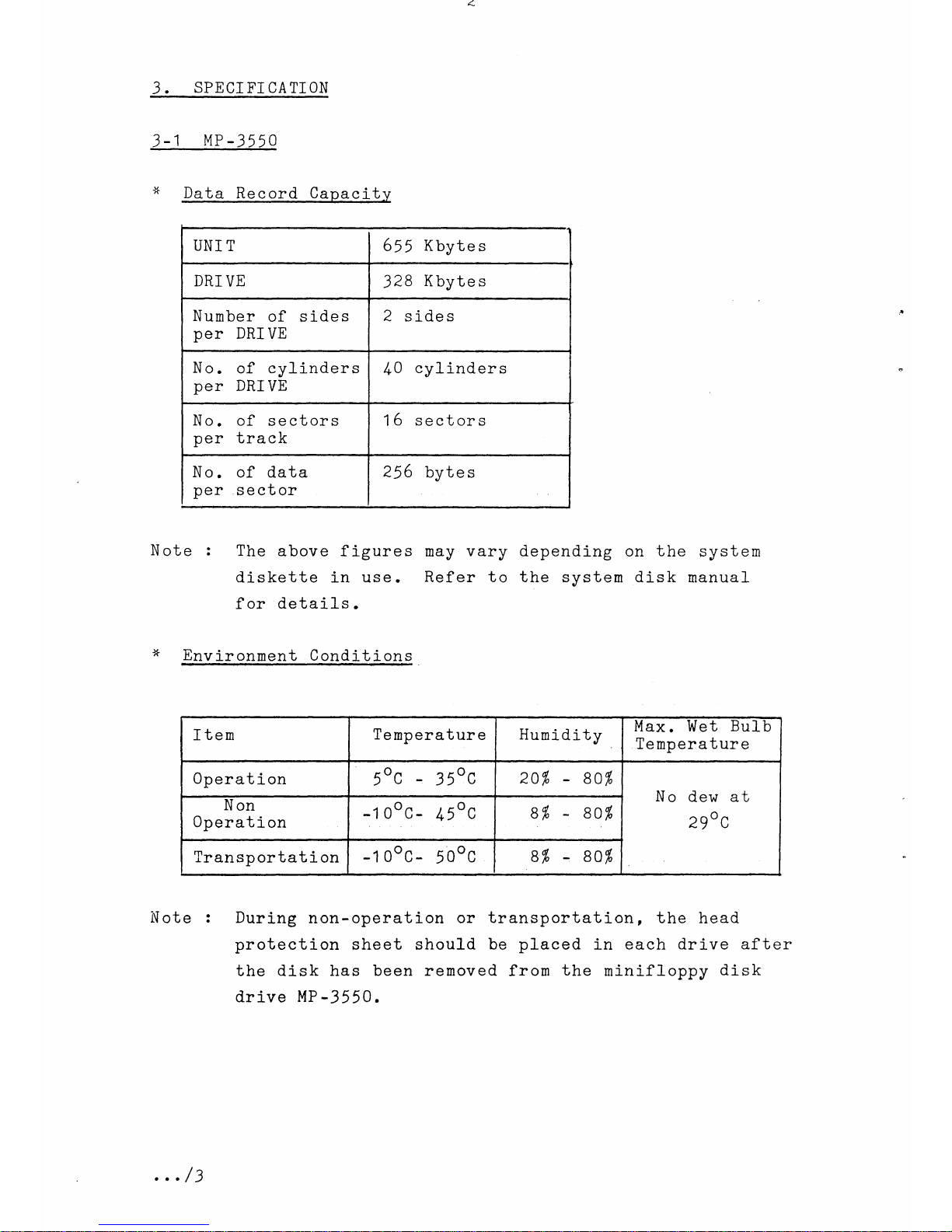
SPECIFICATION
3
-1
tlP
-3550
x
Data
Record Capacitv
UNI T 655 Kbytes
DRI
VE
328
Kbyte
s
Number
of sides
per
DRI VE
2
sides
No.
of cyfinders
per
DRI
VE
/+0
cylinders
No. of
sectors
per track
16 sectors
No. of data
per
sector
256
bytes
Note
:
The
above figures
may
vary depending
on
the
system
diskette
in
use.
Refer to the
system
disk
nanual
f
or details.
*
Environnent
Conditions
ftem
Te
mp erat ur e
Humidity
Max.
Wet
Bulb
Temperature
0perati-on
5oc - 35oc
2or"
gof,
No
dew at
zgo c
Non
0perati
on
-1ooc-
/r5oc
B
1[
8oi[
Tran
sp or tat i on
-1ooc-
5ooc
B% - B0%
Note
:
During
non-operation
or
transportation,
the
head
protection
sheet should
be
placed
in
eaeh drive
afte
the disk has been
removed
from
the
minifloppy
disk
drive
MP
-
3550
.
. . .
/3
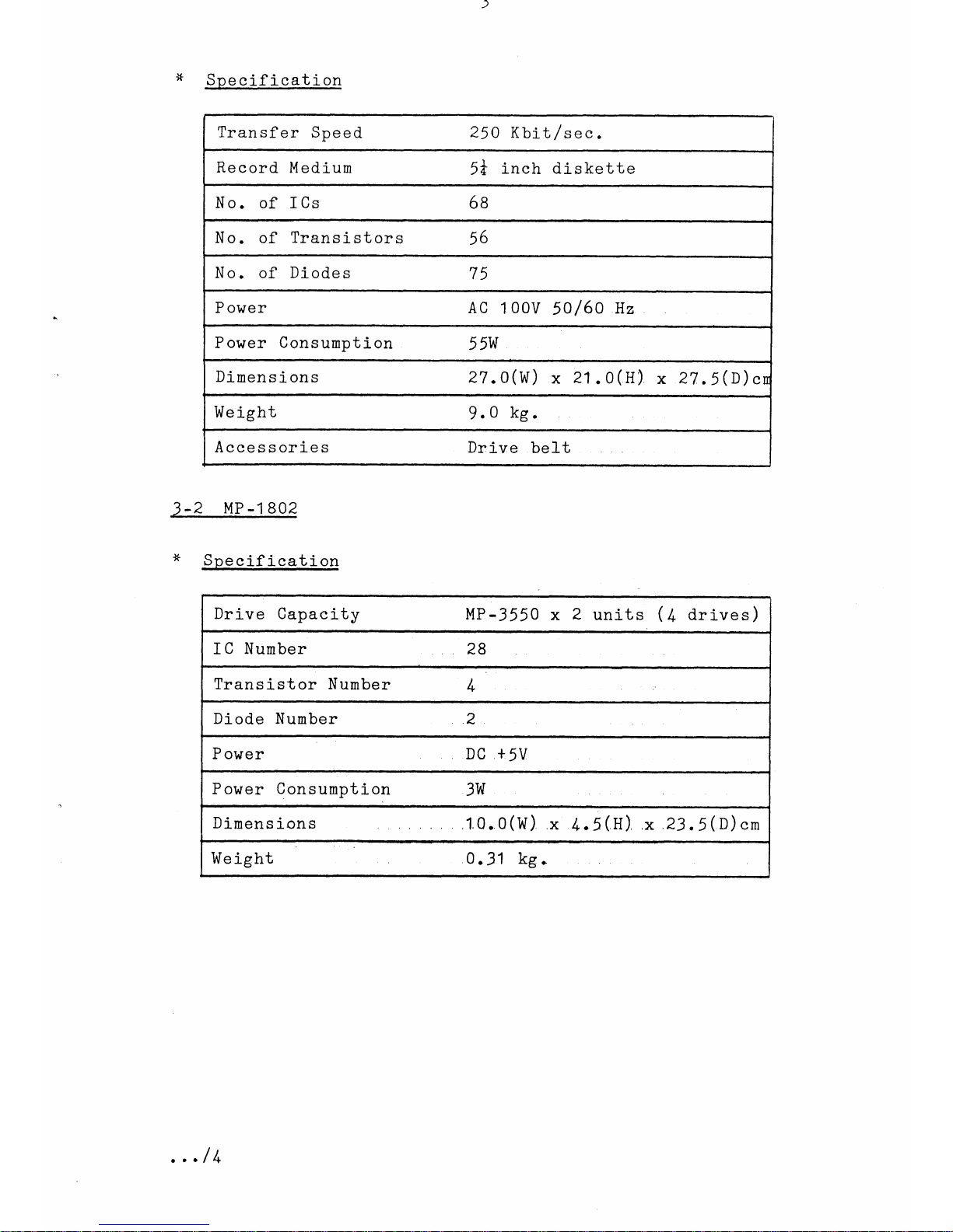
*
Specification
3
-2
t4P
-1
802
*
Spe
cifieation
Transfer
Speed 250
Kbi
L
f
sec
.
Record
Medium
5i
inch diskette
No.
of ICs
6e
No.
of
Transistors
56
No
.
of
Diode
s
75
P
ower
AC
100V
50/60
Hz
Power
Consumption
55W
Dimensions
27.0(W)
x
21
.O(H)
x
27.5(D)cn
We
ight
9.
o
kg.
Accessories
Dr:ive
belt
Drive
Capacity
MP-3550 x 2
units
(lr
drives)
I C Number
28
Transistor Number
lr
Diode Nunber
2
P ower
DC
+5V
Power Consumption
3W
Dirnens
ions
,1.0.0(W)
x
tr.5(jf-)
,x
23.5(D)
cm
We ight 0.31
kg.
.../4.
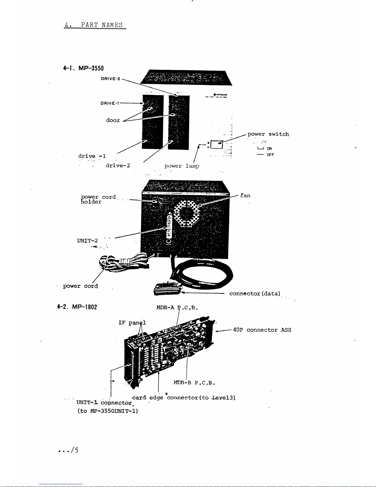
4.
PART
NAI'IES
4-l
.
MP-3550
oRrvE-0
ORIVE.I
drive
-1
drive-
2
power
switch
I roll
_
oFF
power
cord.
holder
fan
connector
(data)
POwer
Ccrrc
+-2. MP-|802
(-to
MP-355OttNIT-l)
l{DB-A
,C,8,
-I{DB-B
P.C.B.
-
'.-3
edge
conneetor
(to
J.eyel3)
power
lamp
.../5
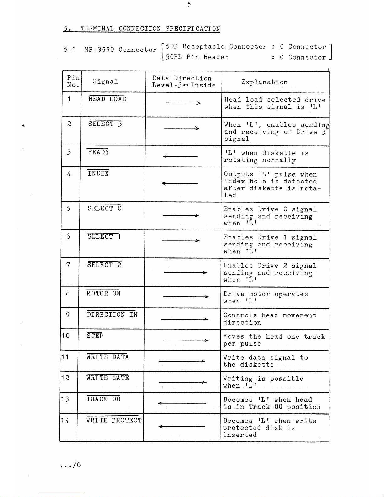
5-1
Mp-
3550
connector
Ilor
Receptac]-e
connector
: c connector
I
I
L
50PL
Pin Header
:
C Connector
J
q
/
5.
TERMINAL
CONNECTTON SPECTFI
CATI..ON
Pin
No.
S
ignal
Data
Direction
Level-3c'
Inside
Expl-anati
on
1
HEAD
LOAD
Head
l-oad selected
drive
when
this signal
is
tL
I
2 SE_IEET-3
___-__--_->
When
rL |
,
enables
sendin5
and
receiving
of
Drive
3
s ignal
3
ET.DY
rL I
when diskette
i-s
rotating
normally
/,
INDEX
<-
Outputs
rLf
pulse
when
index hole
is
detected
after
diskette
is rota-
ted
5
m0
Enables
Drive
0
signal
sending
and
receiving
when
lL I
6 SIET1
------=-+
Enables
Drive
1
signal
sending and
receivi-ns
when
lL I
7
mffi
Enables
Dri've
2
signal
sending
and receiving
when
lL I
8
MOTOR
ON
Drive
motor operates
when
lL I
9
DI
RECTI
ON
IN
Control-s
head
movement
direction
10 S
TEP
t
+
Moves
the
head
one track
per
pulse
11 i[mTETlm
Write
data signal to
the
diskette
12
WRI
TE
GATE
Writing
is
possibl-e
when
tL t
13
TRACK
OO
Becomes
tL
t
when head
is
in
Track 00
position
1l+
WRI
TE
PROTECT
Becones
rL
q
when
write
protected
disk is
inser:ted
...
/6
Pin
No.
S
i
gnal
Data Direction
Level-3**Inside
Explanati
on
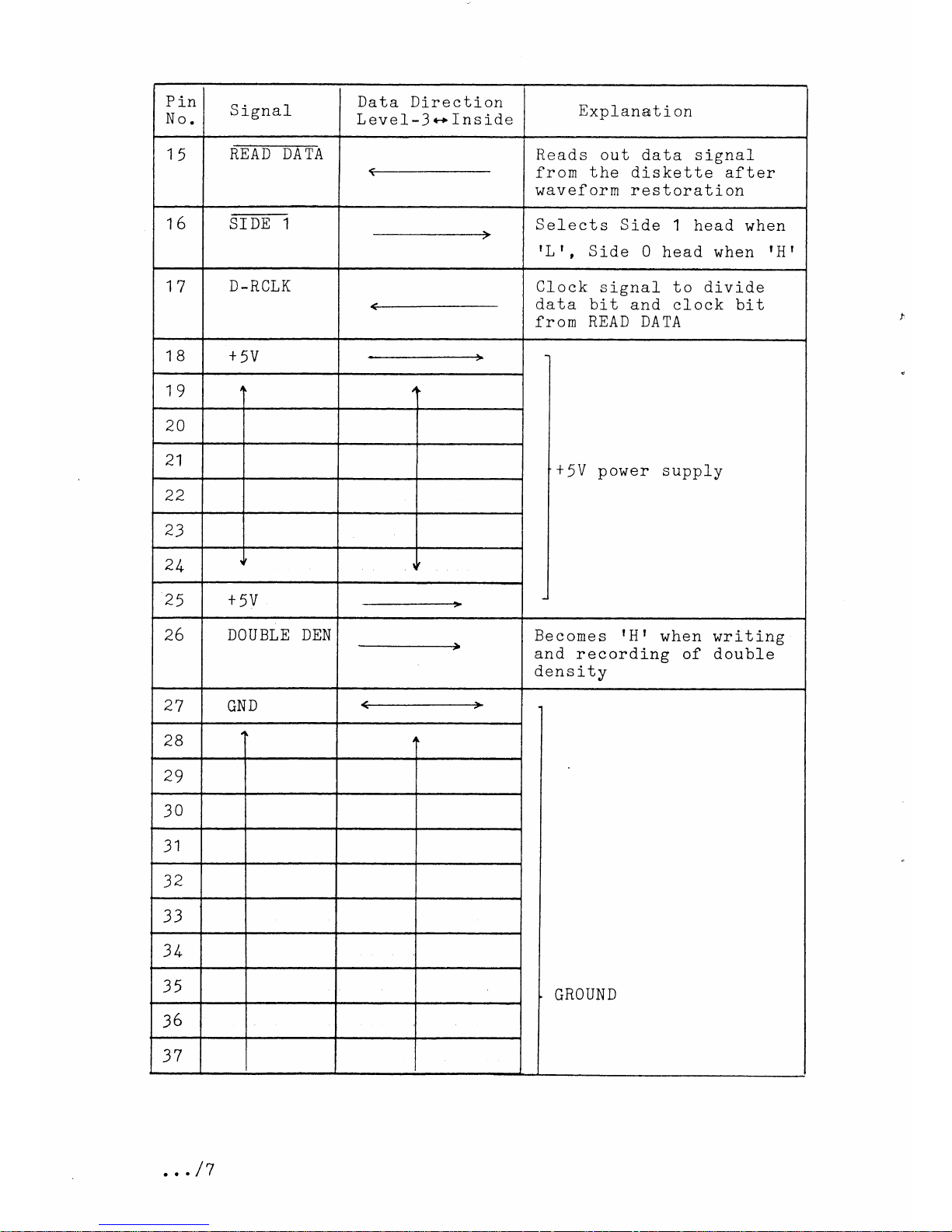
15
READ DATA
Reads
out
data s ignal
from
the
diskette after
waveform restoration
16 mE1
Sel-ects
Side
t head
when
tLt
,
Side
0
head when
tH
t
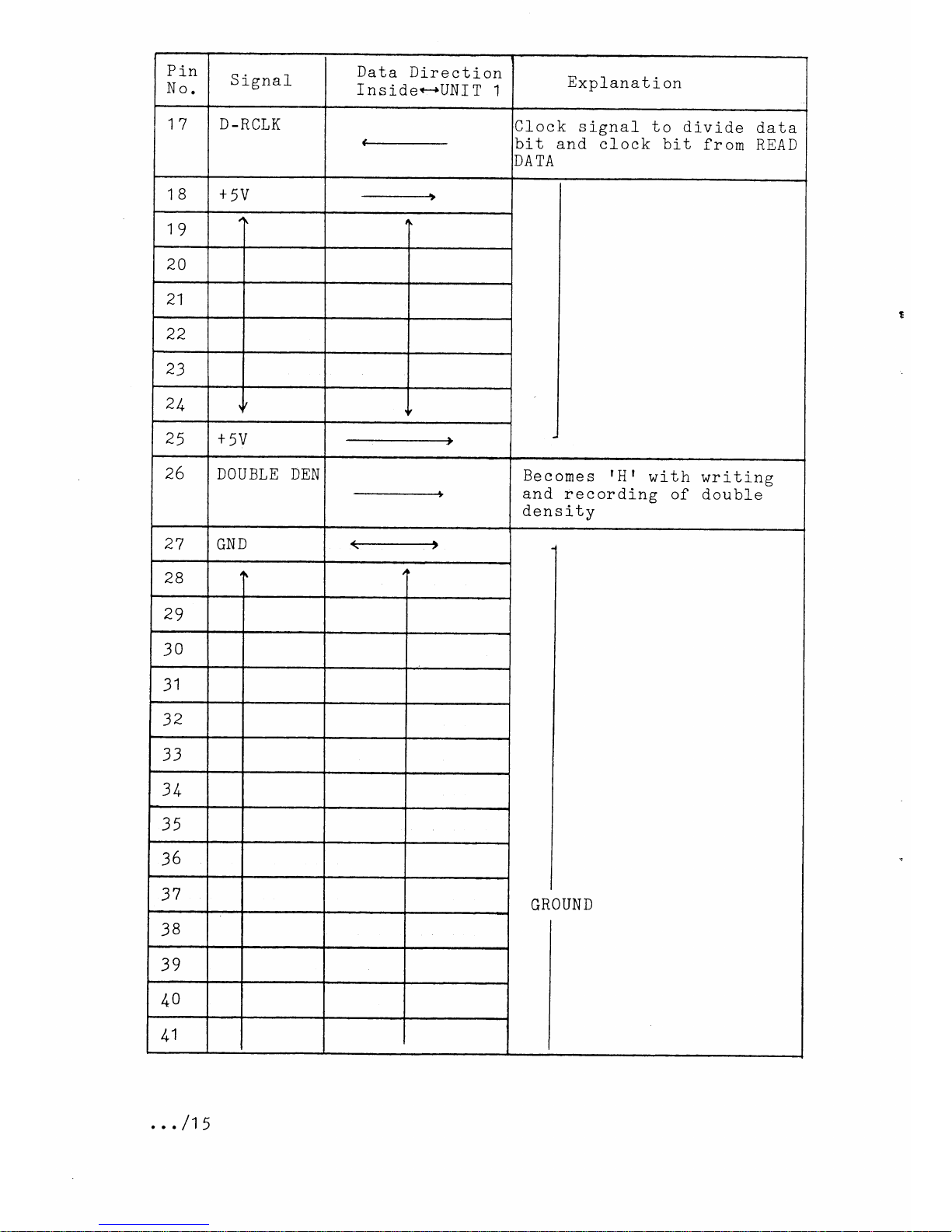
17
D-RCLK
Clock
signal to divide
data
bit
and clock bit
from
READ DATA
1B
+5v
+
5V
power
supply
19
T t
20
21
zz
23
2/,1
J
J
25
+
5v
26
DOUBLE DEN
Becomes
rHr
when writing
and
recording
of double
dens
ity
27
GND
GROUN
D
2B
1 i
2g
30
31
)1
33
3lr
35
36
37
., . /7
Pin
No.
S
igna 1
Data
Direction
Level-3oInside
E*planation
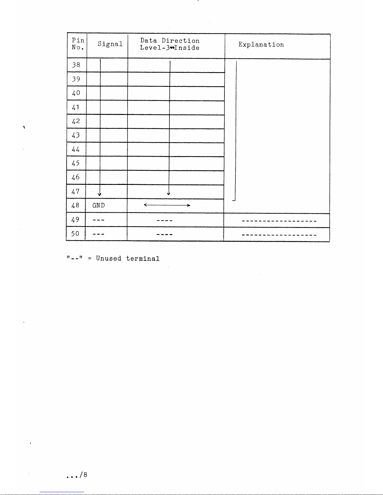
38
39
lr0
/+1
/+2
lr3
/+ lt
lr5
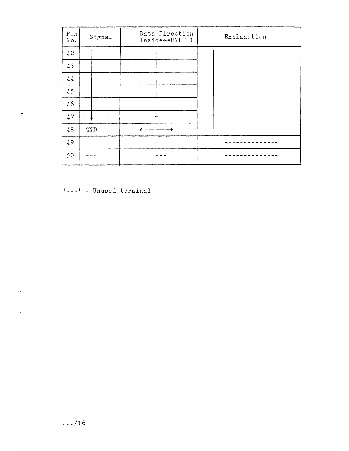
lr6
/+7
J
I
l+8
GND
lr9
50
rr--fr
=
Unused
termi-nal
.../8
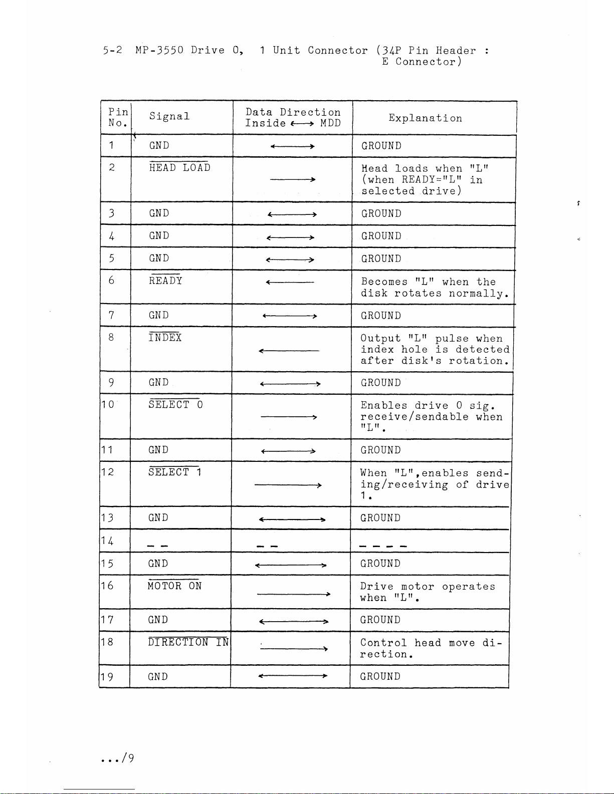
5
-2
MP
-
3550
Drive
0,
1
Unit
Connector
(l
tp
P
in
Header
:
E
Connector
)
Pin
No.
S
ignal
Data
Direction
fnside
H
MDD
Explanation
1
GND
GRO
UN D
z
HEAD
LOAD
-
Head loads
when
rrLrf
(
when
REA
DY
-
rr L tf
in
selected
drive)
1
GND
GRO
UN D
l
4
GND
<---.-->
GRO
UN D
5
GND
GRO
UN
D
6
nnalv
Becomes
rrLrr
when
the
disk rotates norma11y.
7
nnTn
LJII
]J
GROUND
B
INDEX
0utput
tfLrr
pulse
when
i-ndex hole is detected
after
diskrs
rotation.
GND +-+
GRO
UN D
10
Sgi,gCT
O
Enables
drive
0
sig.
receive/sendable
when
Itr
rl
!1
.
11
GND
GRO
UN D
12
SEIEMl
When
rfL
rr
,
enable s s end-
ing
frecei-ving
of
drive
1.
13 GND
GROUN
D
4t
t4
t\
GND GROUND
to
MOTOR
ON
Drive
motor
oDerate
s
when
lf
L
lf
.
17
GND
GRO
UN D
18
m Control
head
move
di-
rection.
1g
GND
GRO
UN D
...
/g
Pin
No.
S
ignal
Data Direction
Inside
c+
MDD
Explanation
20 s-m Moves the head one
track
per pulse
21
GND <-----€
GROUND
22
WRI
TE
DATA
Write data sig. to
the
disk
23
GND
4
GROUND
2/+
WRT
TE
GATE When
frLrr,
enable
write
25
GND
c---------)
GRO
UN D
26 TRACK OO
-------'
Be
c
ome s
fr L rf
when
head
is in
track
00 position
27
cNl
GROUND
2B WRI TE
PROTECT Beeomes
lrLll
when
write
protected
disl
is inserted
2g
GND
-
GROUND
30
READ
DATA
Read
data
s ig . from
the di-sk.
31
GND
<__--------)
GROUND
32
SI
DE.T
Seleet
side
t head
when
frLrtrside
0
heac
when
fr
Hil
33
GND
<___--+
GROUND
3lr
tr
--rr
=
unused
terminal
...
/10
ItJ
5
-3
MP
-
3550
UNI T-2
TERMINAL
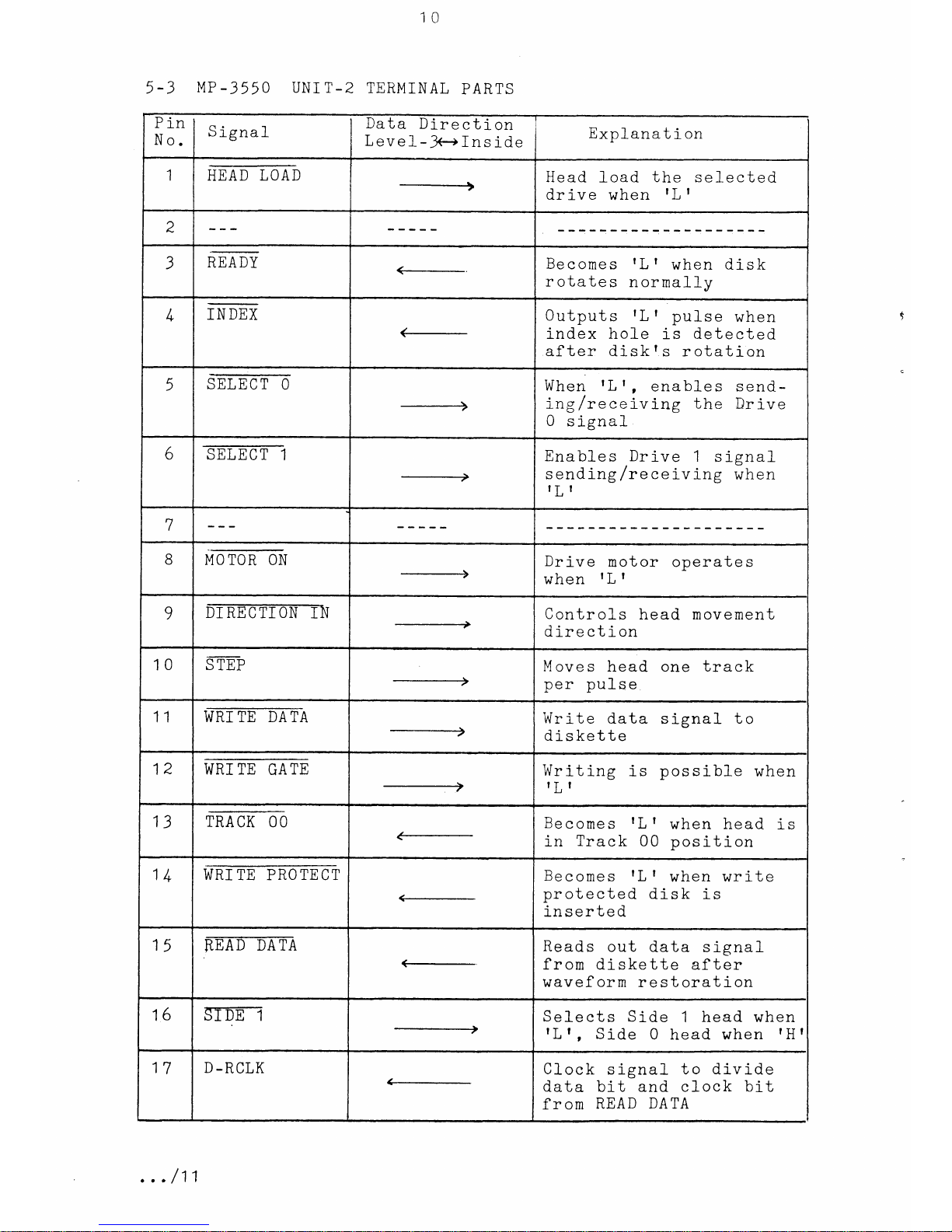
PARTS
Pin
No.
S
ignal
Data
Direction
Level-3<+fnside
Exnlanat
i
on
a
I
HEAD
LOAD
Head
load
the
selected
drive when
rL
I
I
3
REA DY
Becomes
rL
I
when disk
rotates
normally
lr
INDEX
0utputs
rL I
pulse
when
index hole
is
detected
af ter disk
I
s rotati-on
5
SELEcro
When
tL t,
enables send-
itg
f
receiving the
Drive
0
s ignal
6
SELECT
1
--?
Enables Drive
1
signal
s end
ing f r e ce
iv ing
ih"rt
lT I
7
tuoton oll
--->
Drive
motor operate s
when
lL I
9
m
Controls
head movement
direction
10
d mnn
\IHP
V
LJ-IL
M
ove
s head
one track
per puls
e
11
WRI TE DATA
----)
Wr
ite
data
s
ignal
t
o
diskette
12
WRI
TE
GATE
--_-J
Writing
is possible
when
rL
r
13
TRA
CI{ O O
Becomes
rL
I
when head
is
in
Track 00
Dosition
1/+
WRI
TE PROTECT
Becomes
rL
I
when write
protected
disk is
inserted
15
mmIn
F--
Reads
out
data s ignal
from diskette
after
waveform restoration
16
STIE-]
--)
Selects Side'1
head when
rL |
,
Side
0
head
when
rH
t
17
D-RCLK
Cl-ock
signal
to divide
data bit and clock
bit
from
READ DATA
...
/11
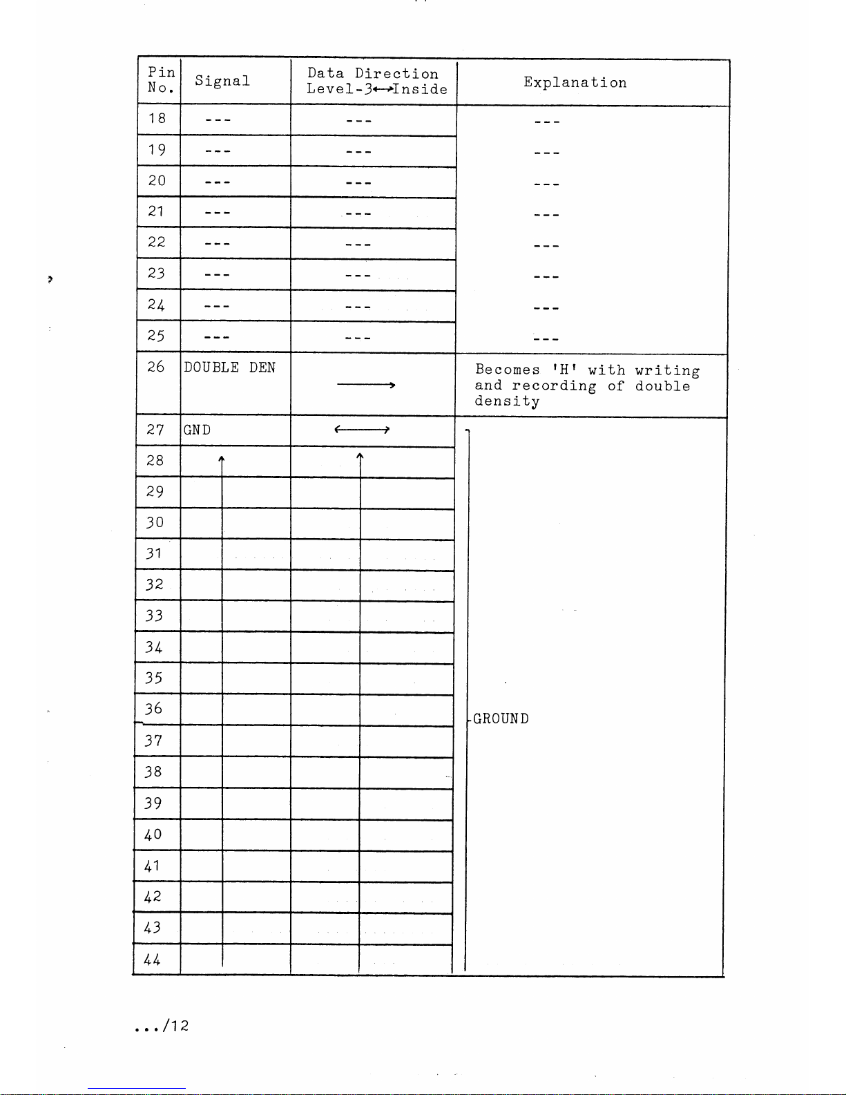
Pin
No.
S
ignal
Data
Direction
Level-3<--.+lnside
Explanation
1B
1g
20
21
22
23
2/+
25
26 DOUBLE
DEN
_-....--
Becomes
fH I
with
writing
and
recording
of
double
dens
ity
27
GND
GROUND
2B
1
2g
30
31
32
33
3L
35
36
37
3B
39
/+0
l+1
l+2
lr3
/, lr
,
.
.
/12
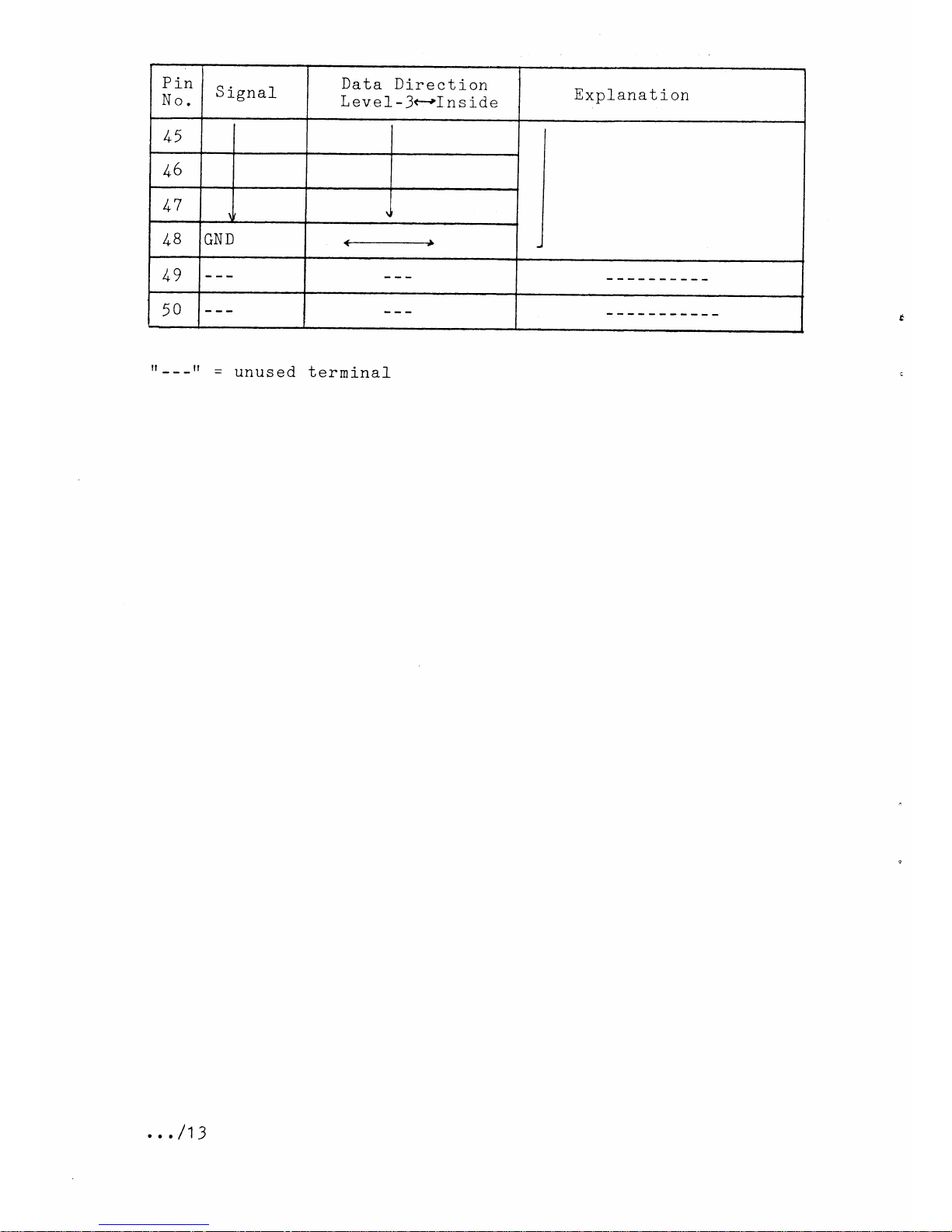
Pin
No,
S
ignal
Data
Direction
Level-3e'-Inside
E*planat
i on
lr5
/r6
t7t
4l
J
/+8
GND
).4
.+/
50
fr---rt
=
unused
terminal
...
/13
5.1
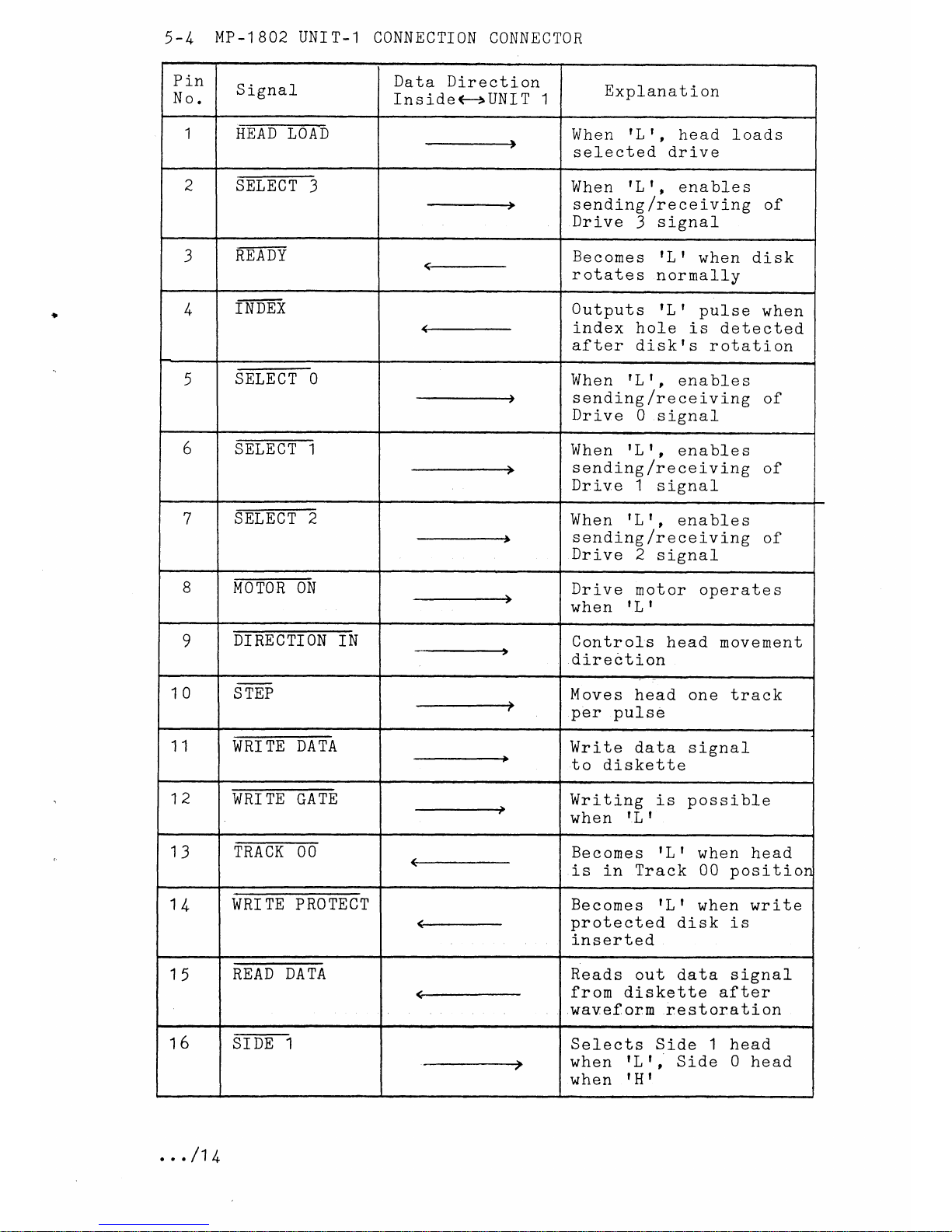
MP-1 BO2 UNI
T.1 CONNECTION
CONNECTOR
Pin
No.
S
ignal
Data Direction
Ins
ide G+UNI T 1
Exol-anation
I
fi]il[D-ImD
When
rL
t,
head loads
selected drive
2 SELECT
3
When
tLt,
enables
sending
freceiving
of
Drive
3
signal
3
MTffi
Becomes
rL
I
when
disk
r
otate
s
normally
/+
rm-ET Outputs
rL I
pulse
when
index
hole
is
dete
cted
after
diskfs rotation
(
ffio
---.9
When
tLr,
enables
sending
freceiving
of
Drive
0
s
ignal
6 SELECT
1
When
tLt,
enables
sending
/"uceiving
of
Drive
1
signal
7
sj;Em
When
rLr,
enables
sending
f
receiving
of
Drive
2
signal
B
MOTOR ON
Drive
motor
oDerate
s
when
rL I
9
DI
RECTION
IN
Contr
ols
head movement
direction
10 S TEP
Moves
head
one track
per pulse
11 WRI
TE
DATA
Write
data signal
to
diskette
12
WRI
TE
GATE
Writing
is
possible
when
rL I
13
TRACI{O6'
Becomes
rL
I
when head
is
in
Track 00 positior
1/+
WRI
TE
PRO
TECT
(-
Becomes
rL
I
when write
protected
disk is
inserted
15
READ
DATA
a-
Reads
out
data
signal
from diskette
after
waveform restoration
16
SIDE
1
.--=+
Selects
Side
t head
when
tLr,
Side
0
head
when
rHr
.
. .
/1/n
Pin
No.
S
igna
1
Data
Direction
f nside.*UNI
T
1
Explanation
17
D-RCLK
Clock
signal
to divide
data
bit and
clock bit
from
READ
DA
TA
18
+5v
1g
t
I
20
21
22
23
2/+
I
I
25
+5v
26
DOUBLE
DEN
Becomes
rHr
with
writing
and
recording
of
double
dens
ity
27
GND
-
GROUND
28
I
2g
30
31
32
33
3lr
35
36
37
38
39
/+0
/,r1
.../15
Pin
No.
S
ignal
Data
Direction
Inside*+UNI T 1
Explanat
i
on
/+2
/r3
/,
lr
lr5
/+6
/+7
I
I
/+8
GND
/-9
50
l---l
=
Unused terminal
.../16
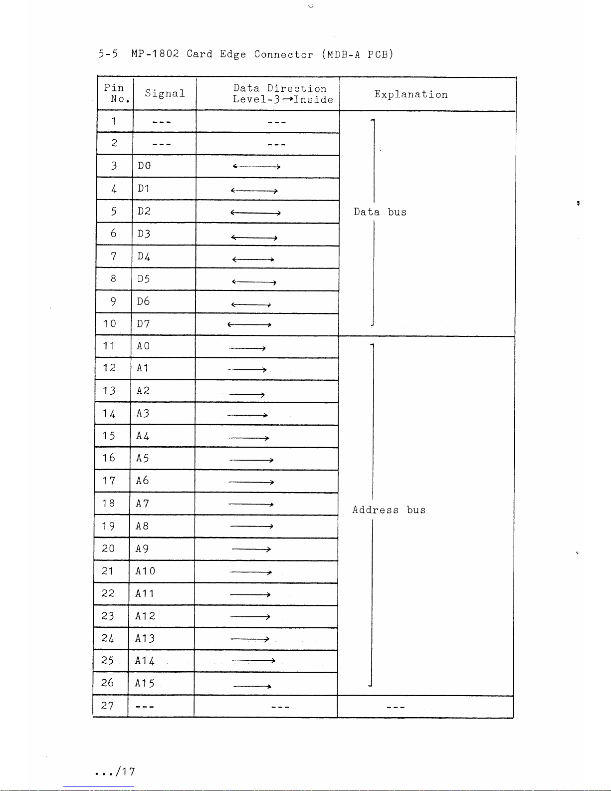
5-5
MP-1802 Card
Edge
Connector
(Unn-A
PCB)
Pin
No.
S
ignal
Data
Directi-on
Level-3;Inside
E"planation
1
Data
bus
2
3
DO
lr
D1
5
D2
(-j
6
D3
7
D/+
<--+
8
D5
c--__J
9
D6
(-________)
10
D7 e------------?
11
AO
.-__)
Addre
s s
bus
12
A1
--.....=-)
13
A2
--
1/+
A3
15
A/+
16
A5
17
A6
18
A7
1g
A8
----=+
20
A9
21 A1 0
--_---+
22
A11
---+
23 A1 2
2lr
A1
3
25
A1 /+
:--::--)
26
A1
5
-----------+
27
.
..
/
j7
Pin
No.
S
ignal
Data
Direction
Level-3
-+Inside
Explanat
i
on
53
5/r
55
rl T\T T\
UNU
GRO
UN
D
)o
rr---rr
=
Unused
terminal
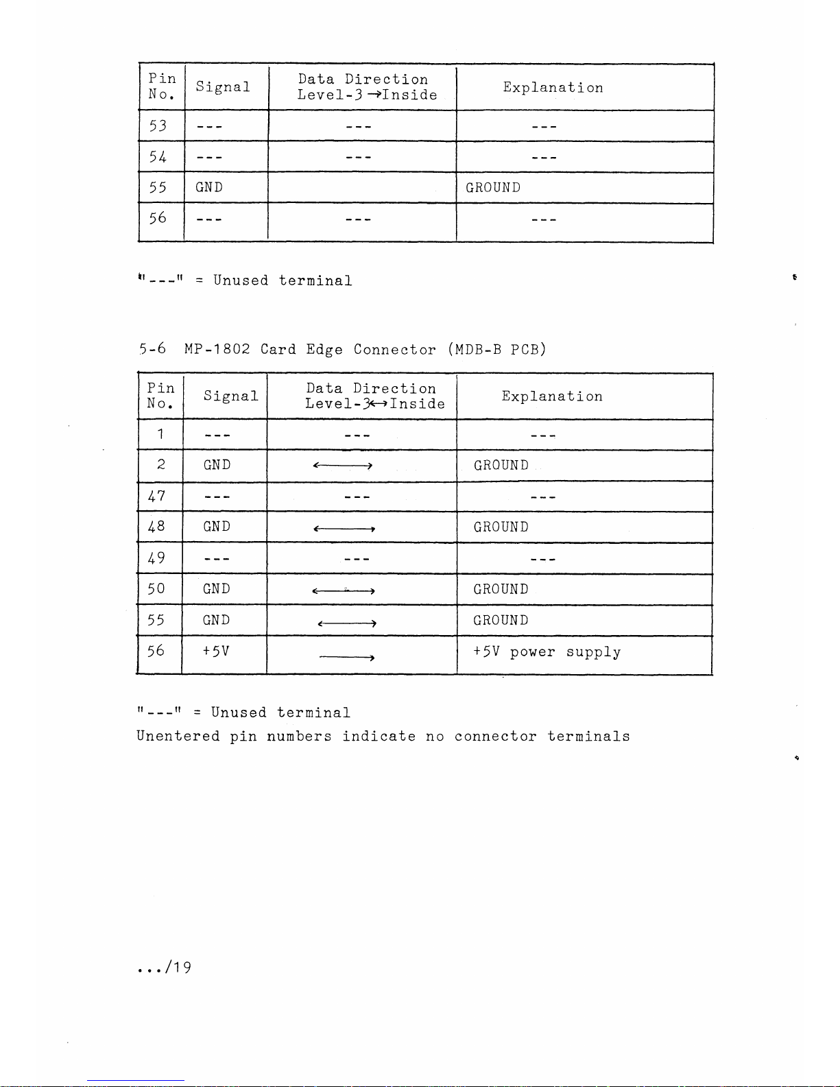
5-6
MP-1802
Card
Edge Connector
(t'lle-n
PCB)
fr---tf
=
Unused
terminal
Unentered
pin
numbers indicate no
connector terminals
Pin
It
II
\J.
S
ignal
Data Direction
Level--.lr.-.Tnside
Explanat
i
on
1
2
rtTTN
\TII
IJ
<____t
GROUN
D
/r7
/+B
GND
<----
GROUN
D
lr9
50
GND
(---€
GROUN
D
55
GND
GROUN
D
56
+5V +
5V
power
supply
...
/19
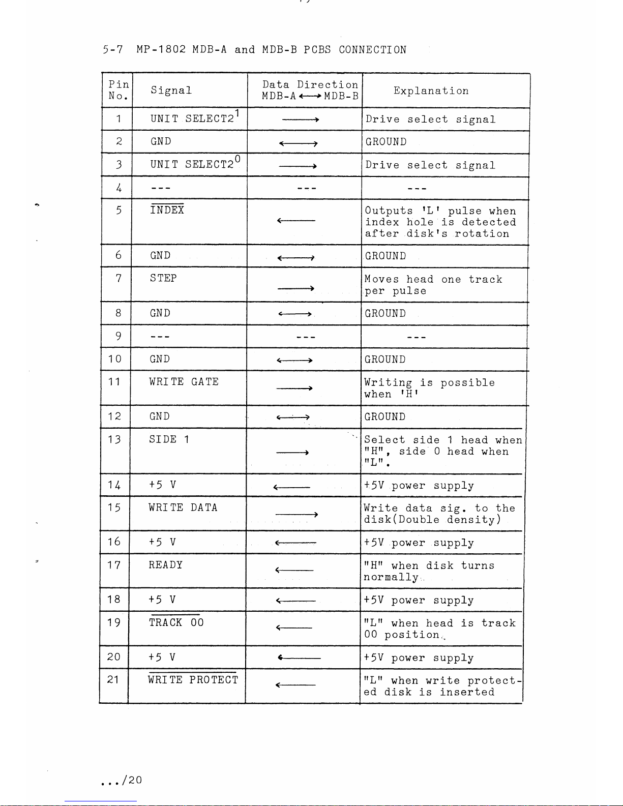
5-7
MP-1802
MDB-A
and
MDB-B
PCBS
CONNECTI0N
Pin
No.
S
ignal
Data
Dire
cti
on
MDB-A
e+
MDB-B
Exol-anat
i on
1
I
UNI T SELE CT21
-----------+
Drive
select
signal
GND
GROUND
3
UNI T SELECT2O
--+
Drive
select
signal
/r
5
INDEX
Outputs
rL t
pulse
when
index hole
is detected
after
diskIs rotation
6
GND
<--
GROUN
D
7
S
TEP
-+
Moves
head one track
per
pulse
8
GND
#
GROUND
9
10 GND <--:-+
GROUND
11
WRI
TE
GATE
Writing
is possible
when
lHf
12
GND
<-+
GROUND
13
SIDE
1
+
Select
side t head
when
rrHfr,
side
0
head when
ilLft.
1/+
+5
V
<-
+
5V
power
supply
15
WRI
TE DATA
Write
data
sie.
to the
disk(Double
d6nsity)
16
+5
V
€-
+5V
power
supply
17
READY
(-
trHfr
when disk
turns
I
normally
I
18
+5
V
+
5V
power
supply
1g
rna clr o o
<-
rrLrr
when head is
track
00
position,..
20
+5
V
6_ +
5V
power
supply
21
WRI
TE
PROTECT
(-
rrLrf
when wri-te
protect-
ed
disk is inserted
.
..
/20
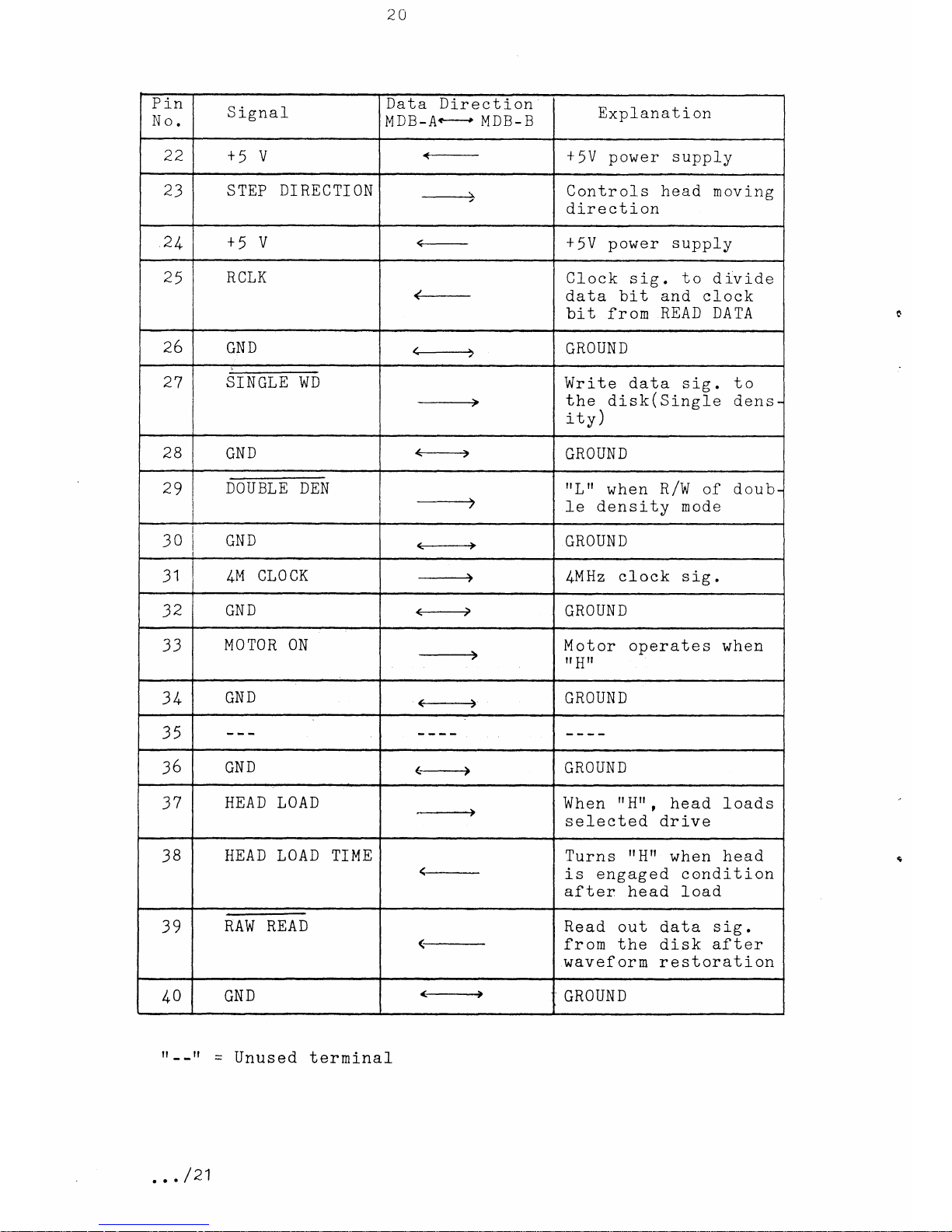
)el
Pin
No.
S
ignal
Data Direction
MDB-Ae
MDB-B
Ex'olanation
22
+5
v
<-
+
5V
power supply
STEP
DIRECTION
t
Controls
head moving
direction
24
+5
v
<-
+
5V
power supply
25
R
CLK
Clock
sig.
to
divide
data bit and clock
bit
from
READ
DATA
26
GND
+--)
GROUN
D
27
SINGLE
WD
Write
data
sig.
to
the
disk
(
Single
d ens
-
ity
)
28
GND
GRO
UN
D
2g DOUBLE DEN
rrLrt
when
R/W
of doub-
Ie density mode
30
GND
€--------)
GROUN
D
31
LI,I
CLO CK
$rlHz
clock
sig.
Jz
GND <-----+
GRO
UN D
33
MOTOR
ON
M
of or
operate
s
when
rr
Hrl
3/,
GND
GROUN D
?(
36
GND
(------)
GROUN
D
37
HEAD LOAD
F_-----)
When
frHrr
,
head loads
seLected dri-ve
38
HEAD LOAD TIME Turns
rr
Hrf
when head
is
engaged condition
after:
head load
39
RAW READ
Read
out
data
s ig
.
from the
disk
after
waveform restoration
/,r0
GND
<-=+
GROUND
rr
- -rf
-
Unused
termi-nal
...
/21
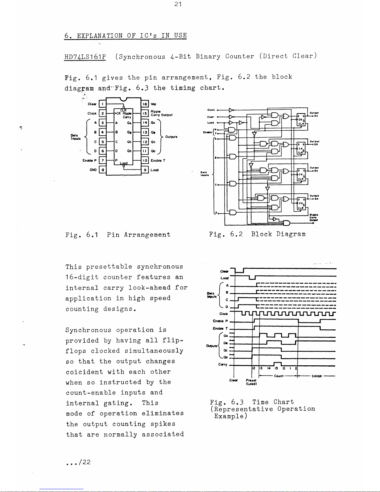
21
HD7 /+LS1
61P
(Synchronous
4-Bit
Binary
Counter
(lirect
Clear
)
Fig
. 6 ,1
give s
the
pin arrangement
,
Fig
.
6.2
the block
diagpan
and"-Fig
.
6
,3
the t iming
ehart
.
Fig
.
6.1
Pin
Arrangement
Fig.
6.2
Block
Diagram
;,.
Corrt
Oufpul
o^)
I
o.
l
>
Oureufr
ocl
u)
.:.'
,j.
'
Ct.o.
Cl o€L
(A
I
I
l8
m&. {
lc
I
'\0
Endb P
GNO
This
presettabl-e synchronous
16-digit counter
features
an
internal
earry
look-ahead
for
applieati-on
in high speed
counting
designs.
Syrchronous
operation
is
provided
by having
all flip-
flops
clocked
s imultaneously
so
that
the
output changes
coicident
with
each other
when
so
instructed
by
the
c ount
-
enabl-e
input s
and
internal-
gating.
Thj-s
mode
of
operation
elininates
the
output
counting spikes
that
are
normally
as s
oci-ated
Fie
.
6.3
Time Chart
(
n6presentative
Operation
Exarrple
)
k
Lood
(a
I
ooro )
s
t+utr)
lc
Lo
J1
€ncde t
(o^
I
lOr
o.rwn1
lft
Lo
Cary
Chc Pnrl
(t-oodl
.. . /22
with asynchronous
(
ripple clock)
counters
.
A
buffered
clock
input
triggers
the
four flip-f1ops
on
the
rising
(positive-
going
)
edge of the
clock
lnput waveform.
This
counter
is f u11y progranmabl-e;
that
is,
the outputs
may
be
preset
to
either
I
H
I
and
rL I
level, As
presetting
is
synchronous,
setting
up
a l-ow level at
the
load input
disables
the
counter and causes
the
outputs to
agree
with
the
setup
data
after
the
next
cl-ock
pulse
regardl-ess
of the
levels
of
the enable
inputs. Low-to-high
transiti-ons
at
the
load
input
should
be
avoided
when the clock
is lor^r
if
the
enable inputs
are
high at or before
the
transition.
The
clear
function
is asynehronous
and a
low l-evel
at the clear
input
sets all
four of
the
flip-flop
outputs
low
regardless
of
the
levels
of
c1ock, load, or
enable
input s
.
The
carry
look-ahead
circuitry
provides
for
cascading
counters
for n-bit synchronous
appl-ications
without
additional
gating.
f nstrumental
in
accomplishing this
function
are
two
count-enable
inputs
and
a
ripple
earry
output.
Both
c ount - enabl-e
input s
(p
and
T
)
must
be
high
to
count,
and
input
T
is fed
forward
to
enable
the ripple carry
output. The
ripple carry
output thus
enabled
wil-l
pr oduce
high vel output
puls
e
with a duration
approximately
equal to
the high-level portion
of the
QA
output,
This
high-level
overflow
ripple
carry
pulse
can be
used to
enable
successive
cascaded
stages. High-to-1ow
1evel
trans-
itions
at
the
enable P
or T inputs should
occur onlv
when
the
clock
input is high.
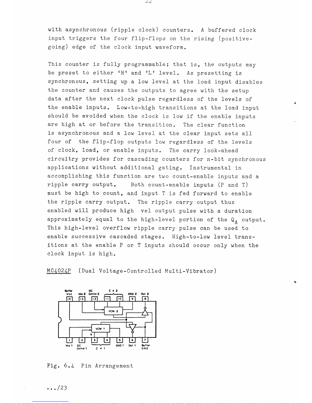
I4C/+0.2/+P
(
Dual
Voltage-Controlled
Mu1ti-Vibrator)
vcc
I
oc
--t-J
Gt{o
I
orr?
I
Cnlrolt
C
r
t
Fig. 6./,,
,
,
,
/23
&rf
lrr
G
r{0
Pin
Arrangement

Fig
'
6
'
/n
shows
the
pin
arrangement.
This
is
two
vcMs
(voltage-
controlled
multi-vibrators
)
with
output
buffer,
The
oseillating
frequency
is
controlled
by
the
DC
voltage
applied
to
the
DC
control-
terminal
and.
is
used
f
or
the
pLL
(phase
Locked
Loop
)
in
digital-
ci-rcuit
wlth
the
phase
Detector
(uc4a/n/).
I,ICl,0L/r!
(phase
Detector)
Rcf
crcnco
oorn I vdiobla
Llg
tn up
ort
oorn
2 Gt{o
Fig
.
6,5
Pin
Arrangement
Oottr
9p5r
11raP
Vcc
Up
r
W
2
la
Ou||
t||
qJTruT
The
pin
arrangement
is
consists
of
two
phase
is
used
in
the
ptl
in
(uc
402
/+p
)
.
given
above
in
Fig
.
6.5
. The
I C
detectors,
a
eharge
purnp
and
AMp.
ft
digital-
circuit
together
with
the
vcM
Phase
Detector
#l
and
#z
are
used
when
the
input
signal
to
the
Variable
termi_nal
is
delayed
0o
and
90o
fron
the
input
signal
to
the
Reference
termi-nar.
(trre
input
signal
at#2
Reference
and.
variabre
terninars
must
have
501, duty.
)
It
outputs
a
pulse
(rr;96rr
which
corresponds
to
the
falling
edge
phases
input
The
charge
punp
D=tr1tt
and
U=ttLtt)
When
the
lnput
signal
phase
and
Variable
terminals,
the
i
mpedanc
e
.
(
fne
s
ignal
f1
ow
..,/2/,
active
)
to
the
Up,
Down
terminal_
difference
of
two
digital
signal
to
the
Reference,
Variable
terninals.
converts
the
phase
fast
or
delay
(respectivery
to
either
q9V
or
2.3V.
difference
is
0o
at
the
Reference
charge
pump
output
becomes
high
sets
Up1
(UpZ)
to Up
fN,
Downl
Rcfcrcnco
Oorn I Vdiobla
(
Down2
)
to
Down
IN
and
Up OUT,
Down OUT
to
make AMP IN.
)
r1
l.
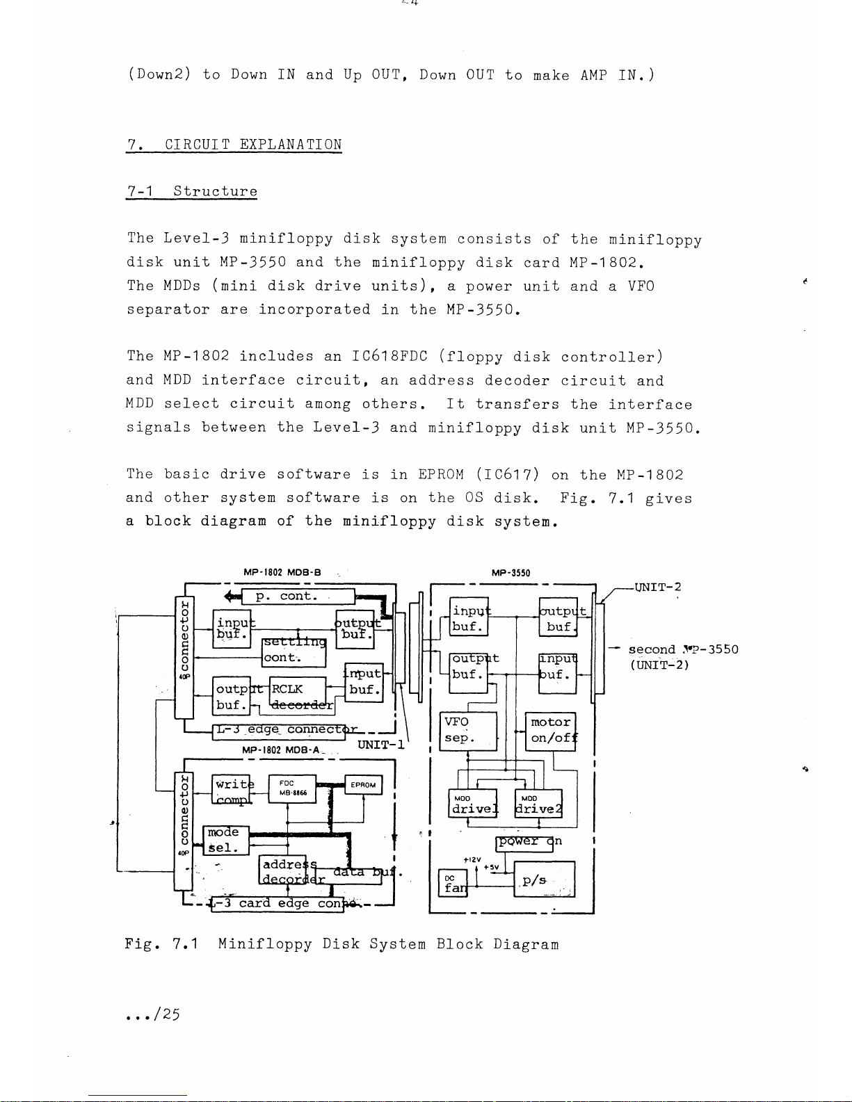
CI R
CUI T EXPLANA TI ON
7
-1
Structure
The
LeveL-3
minifloppy disk
system
consists
of the
minifloppy
disk unit
MP
-
3550
and the
minifloppy
disk
card MP
-1
802.
The
MDDs
(mini
disk drive
units),
a
power
unit and a
VFO
sep
ayator are i-ncorporated
in
the MP
-
3550.
The
MP-1802
includes
an
IC61
SFDC
(floppy
disk
controller)
and MDD
interf
ace
ci-rcuit,
an address
decoder circuit
and
MDD
select ci-rcuit among
others
.
f t transf
ers
the
interf
ace
signals
between the Lev
eI-3
and
minifloppy
disk
unit
MP
-
3550.
The
basic
drive software
is in
EPROM
(IC61
7)
on the MP
-1
802
and other
system software
is
on
the
0S
disk. Fig.
7.1
gives
a bl-ock
diagran
of the
ninif f oppy disk
system.
MP.I8O2
MOB-B
MP-3550
LINTT-2
sgcqnd .t?-
3550
(
uNrr-2
)
Fig.
7.1
I
-J
t{
o
+J
o
c)
tr
H
o
o
r0P
rnpu
buf.
tl
o
+)
o
o
c
q
o
(J
a0P
,
.
.
/25
Minifloppy
Disk
System Bl-ock
Diagram
(1)
Recordins
Medium
As
shown
in Fig
.
7.2, the
double_sided
double
density
5*
inch
diskette (fte*_
ible
or
floppy
disk)
is
used
as
the
recording
medium
in
the
li,lp
_
3550.
Inside
there
is
a
magnetic
disk
and
the
recording
is
done
on
concentric
tracks,
and
dividing
the
track
i-nto
snaller
units,
on
sectors.
sector
./,
'
,/t
(a)
Fig.7.2
(r)
Fig
.
7.3
5t
Inch
Disk
Construction
write
protect
center
hole
index
hole
head
window
head
coqtact
gnetic
disk
iner
acket
(2)
Recording/Readlng
MFM
Recording
Method
.-.
-
,
'
M
ethods
(uoaified
Frequency
Br
e
akd
own
of
Recording
Unit
Modul-ation)
(
i)
write
the
data
bit
in
the
centre
of
the
bit
cell
The
MFM
method
is
used
for
FDD
recording.
This
method
(ii)
Write
the
clock
cell
if
no
data
bit
celI
or
the
Fig
.
7
.
/,
compares
the
A1
reeording
method
and
MFM
double
-sided
d.oubl_e
dens
ity
must
conf
orm
with
these
rul_es:
bit
at
the
head
of
the
present
bit
bit
is
written
in
either
the
previous
pre
sent
bit
ee1l
pattern
written
with
the
FM
recordirg
method.
Unlike
the
FM
t
.
,
.
/26
 Loading...