

Page 1

SERVICE MANUAL
MANUEL D'ENTRETIEN
WARTUNGSHANDBUCH
CAUTION:
Before servicing this chassis, it is important that the service technician read the “Safety
Precautions” and “Product Safety Notices” in this service manual.
No. 0257
L19DP04U
L19HP04E
L19HP04U
L22DP04E
L22DP04U
L22DP04UA
L22HP04E
L22HP04U
D a t a c o n t a i n e d w i t h i n t h i s S e r v i c e
manual is subject to alteration for
improvement.
ATTENTION:
Avant d’effectuer l’entretien du châssis, le technicien doit lire les «Précautions de sécurité»
et les «Notices de sécurité du produit» présentés dans le présent manuel.
VORSICHT:
Vor Öffnen des Gehäuses hat der Service-Ingenieur die „Sicherheitshinweise“ und „Hinweise
zur Produktsicherheit“ in diesem Wartungshandbuch zu lesen.
FOR ALL PARTS PLEASE MAKE
CONTACT WITH ASWO.
FOR YOUR LOCAL OUTLET GO TO
Les données fournies dans le présent
manuel d’entretien peuvent faire l’objet
de modifications en vue de perfectionner
le produit.
D i e i n d i e s e m Wa r t u n g s h a n d b u c h
enthaltenen Spezifikationen können sich
zwecks Verbesserungen ändern.
www.aswo.com
SPECIFICATIONSANDPARTSARESUBJECTTOCHANGEFORIMPROVEMENT
Colour Television
August 2009
Page 2

THIS PAGE INTENTIONALLY
LEFT BLANK
Page 3

1 INTRODUCTION.............................................................................................................. 5
2 TUNER............................................................................................................................... 5
2.1 General description of TDTC-G101D: ........................................................................ 5
2.2 Features of TDTC-G101D: .......................................................................................... 6
2.3 Pin Configuration: ........................................................................................................ 7
3 SAW FILTER ......................................................................................................................... 7
3.1 IF Filter for Audio Applications – Epcos K9656M ..................................................... 7
3.1.1 Standarts .................................................................................................................... 7
3.1.2 Features ..................................................................................................................... 7
3.1.3 Pin Configuration ...................................................................................................... 7
3.1.4 Frequency Response.................................................................................................. 8
3.2 IF Filter for Video Applications – Epcos K3958M................................................... 9
3.2.1 Standarts .................................................................................................................... 9
3.2.2 Features ..................................................................................................................... 9
3.2.3 Pin Configuration ...................................................................................................... 9
3.2.4 Frequency Response.................................................................................................. 9
4 AUDIO AMPLIFIER STAGE WITH PT2333.................................................................... 10
4.1 General Description of PT2333: ................................................................................ 10
4.2 Features of PT2333: .................................................................................................. 10
4.3 Pin Configuration of PT2333: ................................................................................... 11
5 MICROCONTROLLER (MSTAR)..................................................................................... 11
5.1 Genaral Description.................................................................................................... 11
5.2 Features ...................................................................................................................... 12
6 INTEGRATED DVB-T RECEIVER (CHEERTEK) ........................................................... 13
6.1 General Description.................................................................................................... 13
6.2 Features ...................................................................................................................... 13
7. 4MX16 BIT SYNCHRONOUS DRAM ( DIGITAL SIDE SDRAM) ................................ 16
7.1 General Description.................................................................................................... 16
7.2 Features ...................................................................................................................... 16
7.3 Pin Configuration ....................................................................................................... 17
8 S25FL016A - 16 Megabit Cmos 3.0 Volt Flash Memory with 50-Mhz (Serial Peripheral
Interface)Bus………………………………………………………………………………….18
8.1 General Description.................................................................................................... 18
8.2 Distinctive Characteristics.......................................................................................... 18
9 4M x 16 bit Synchronous DRAM (ANALOG SIDE SDRAM)............................................ 20
9.1 General Description................................................................................................... 20
9.2 Features ...................................................................................................................... 20
9.3 Pinning ....................................................................................................................... 21
10 POWER STAGE ................................................................................................................. 22
10.1 IPS 15 Option ........................................................................................................... 22
11 IC SPECIFICATIONS ........................................................................................................ 23
11.1 8K Smart Serial EEPROM – 24C64 ....................................................................... 23
11.2 TL062 ...................................................................................................................... 24
11.3 FSA3157.................................................................................................................. 25
11.4 FDS8878.................................................................................................................. 26
11.5 ST24LC21 (Optional) ............................................................................................. 26
11.6 TDA1308T .............................................................................................................. 27
11.7 STMP2161 .............................................................................................................. 28
11.8 AZ1045....................................................................................................................30
11.9 MP1583 ................................................................................................................... 31
3
Page 4

11.10 LM1117................................................................................................................. 33
11.11 MP2109 ................................................................................................................. 34
11.12 FDC642P............................................................................................................... 35
11.13 XC5000 (Optional)................................................................................................ 36
12 BLOCK DIAGRAMS ......................................................................................................... 39
12.1 General Block Diagram.......................................................................................... 39
12.2 Integrated DVB-T Receiver Block Diagram.......................................................... 41
12.3 17MB45 Analog Front-End ................................................................................... 42
12.4 17MB45 Digital Front-End .................................................................................... 42
12.5 17MB45 Digital CI ve Smart Card Interface ......................................................... 43
12.6 17MB45 HDMI Inputs ........................................................................................... 43
12.7 17MB45 Analog Interface “ MSTAR IC “ ............................................................ 44
12.8 17MB45 Analog Input / Output ............................................................................ 45
12.9 17MB45 LVDS Output .......................................................................................... 45
12.10 17MB45 Power ...................................................................................................... 46
4
Page 5

1 INTRODUCTION
17MB45-2 mainboard is based on MSTAR concept IC. This IC is capable of handling audio
processing, video processing, scaling-display processing, 2D comb filter, OSD and text
processing, 8 bit dual LVDS transmitter.
TV supports PAL, SECAM, NTSC colour standards and multiple transmission standards as
B/G, D/K, I/I’, and L/L’ including German and NICAM stereo.
Sound system is able to supply 2x2.5W (10%THD) audio output power for stereo speakers.
Supported peripherals are:
The analog part of the moard can support DVD module which is connected to mainboard
through a cable.
The USB feature is supported through digital part of the mainboard.
1 RF input VHF1, VHF3, UHF @ 75Ohm(Common)
1 Side AV (CVBS, R/L_Audio) (Common)
1 SCART socket(Common)
1 PC input(Common)
1 Headphone(Optional)
1 Common interface(Optional)
1 Digital USB(Optional)
1 HDMI (Optional)
2 TUNER
A horizontal mounted and Digital Half-Nim tuner is used in the product, which covers 3
Bands(From 48MHz to 862MHz for COFDM, from 45.25MHz to 863.25MHz for CCIR CH).
The tuning is available through the digitally controlled I2C bus (PLL). Below you will find
info on the Tuner in use.
2.1 General description of TDTC-G101D:
The Tuner covers 3 Bands(from 48MHz to 862MHz for COFDM, from 45.25MHz to
863.25MHz for CCIR CH). Band selection and Tuning are performed digitally via the I2C
bus.
5
Page 6
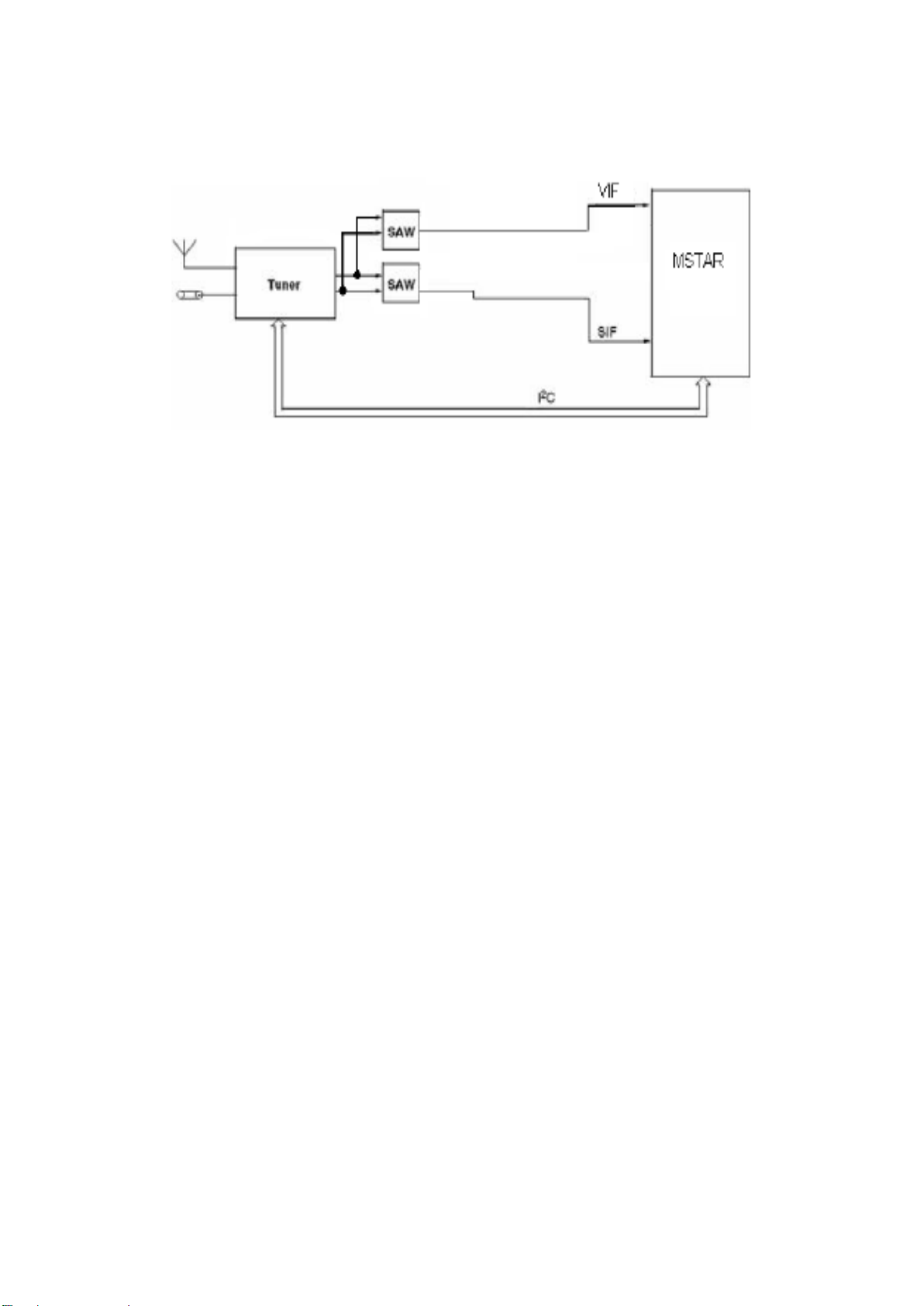
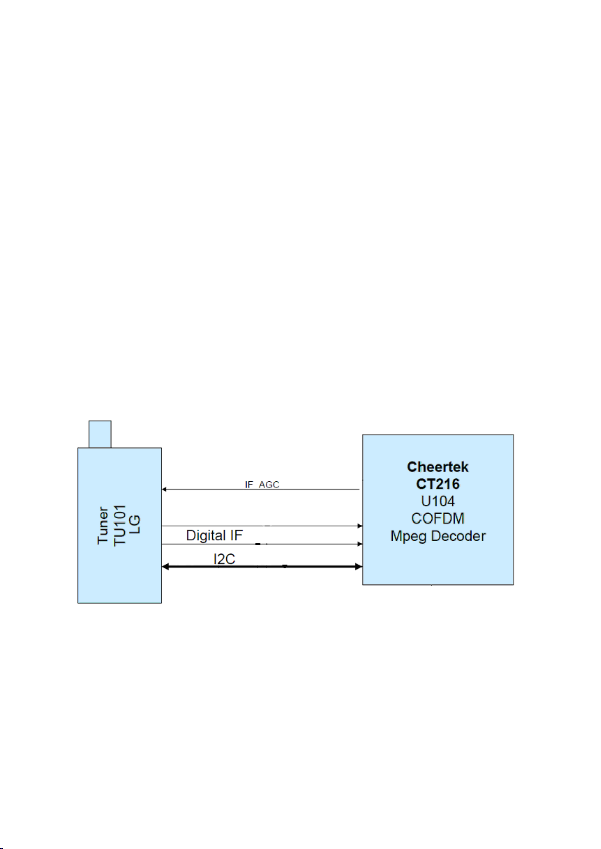
Tuner and Main IC connections for analog:
2.2 Features of TDTC-G101D:
x Digital Half-NIM tuner for COFDM
x Covers 3 Bands(From 48MHz to 862MHz for COFDM,
x From 45.25MHz to 863.25MHz for CCIR CH)
x Including IF AGC with SAW Filter
x Bandwidth Switching (7/8 MHz) possible
x DC/DC Converter built in for Tuning Voltage
x Internal(or External) RF AGC, Antenna Power Optional
6
Page 7
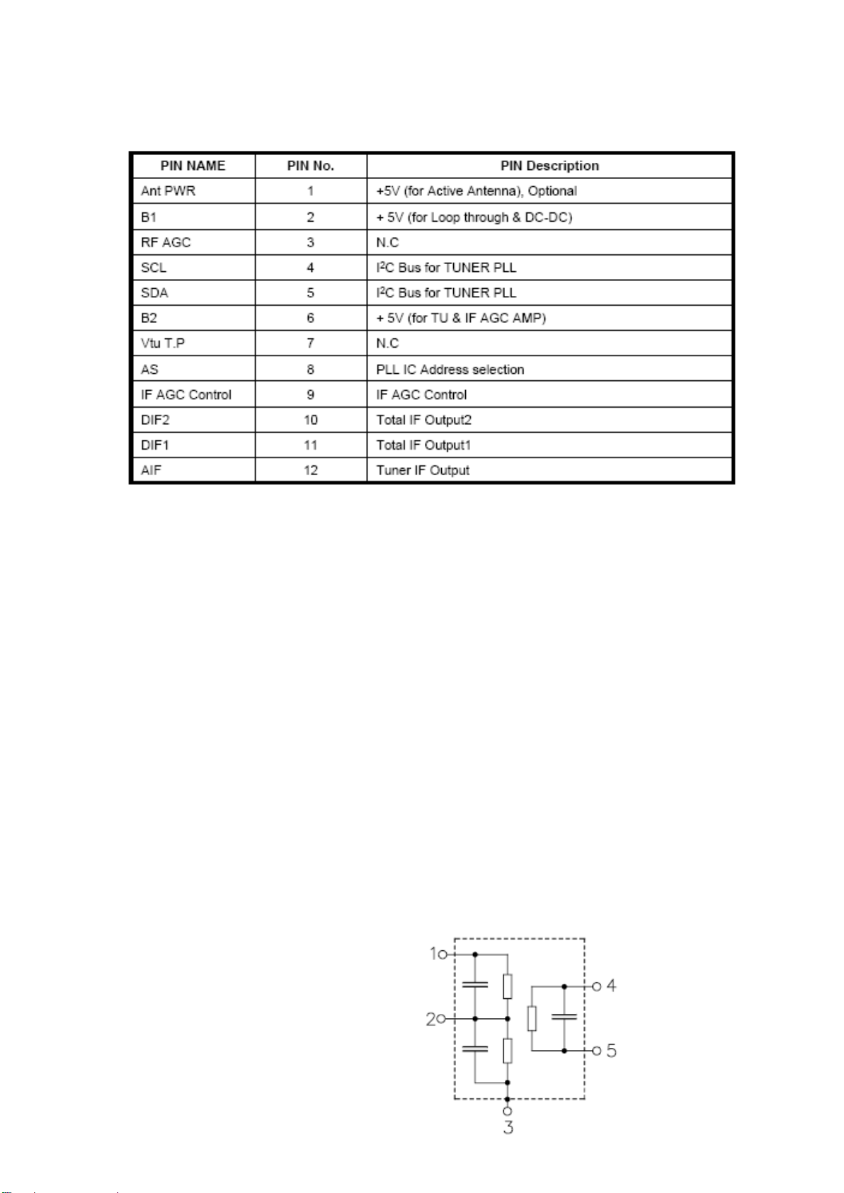
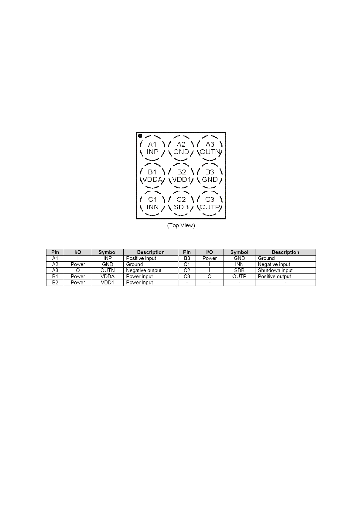
2.3 Pin Configuration:
3 SAW FILTER
3.1 IF Filter for Audio Applications – Epcos K9656M
3.1.1 Standarts
x B/G
x D/K
x I
x L/L’
3.1.2 Features
x TV IF audio filter with two channels
x Channel 1 (L’) with one pass band for sound carriers at 40,40 MHz (L’) and 39,75
MHz (L’- NICAM)
x Channel 2 (B/G,D/K,L,I) with one pass band for sound carriers between 32,35 MHz
and 33,40 MHz
3.1.3 Pin Configuration
1 Input
2 Switching input
3 Chip carrier - ground
4 Output
5 Output
7
Page 8
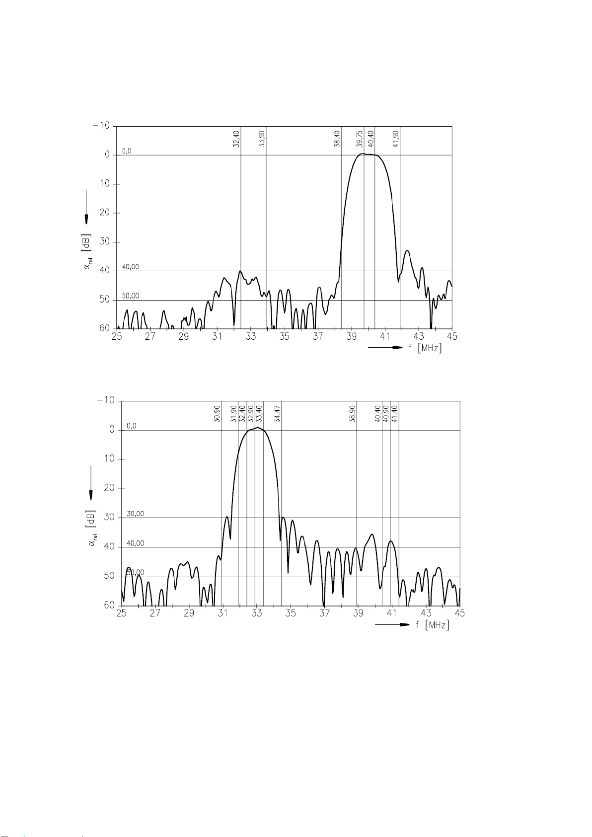
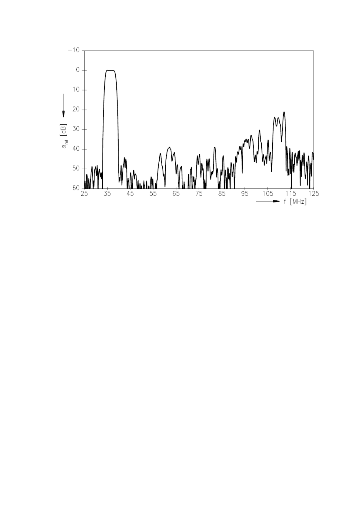
3.1.4 Frequency Response
Frequency Response of Channel 1:
Frequency Response of Channel 2:
8
Page 9
3.2 IF Filter for Video Applications – Epcos K3958M
3.2.1 Standarts
x B/G
x D/K
x I
x L/L’
3.2.2 Features
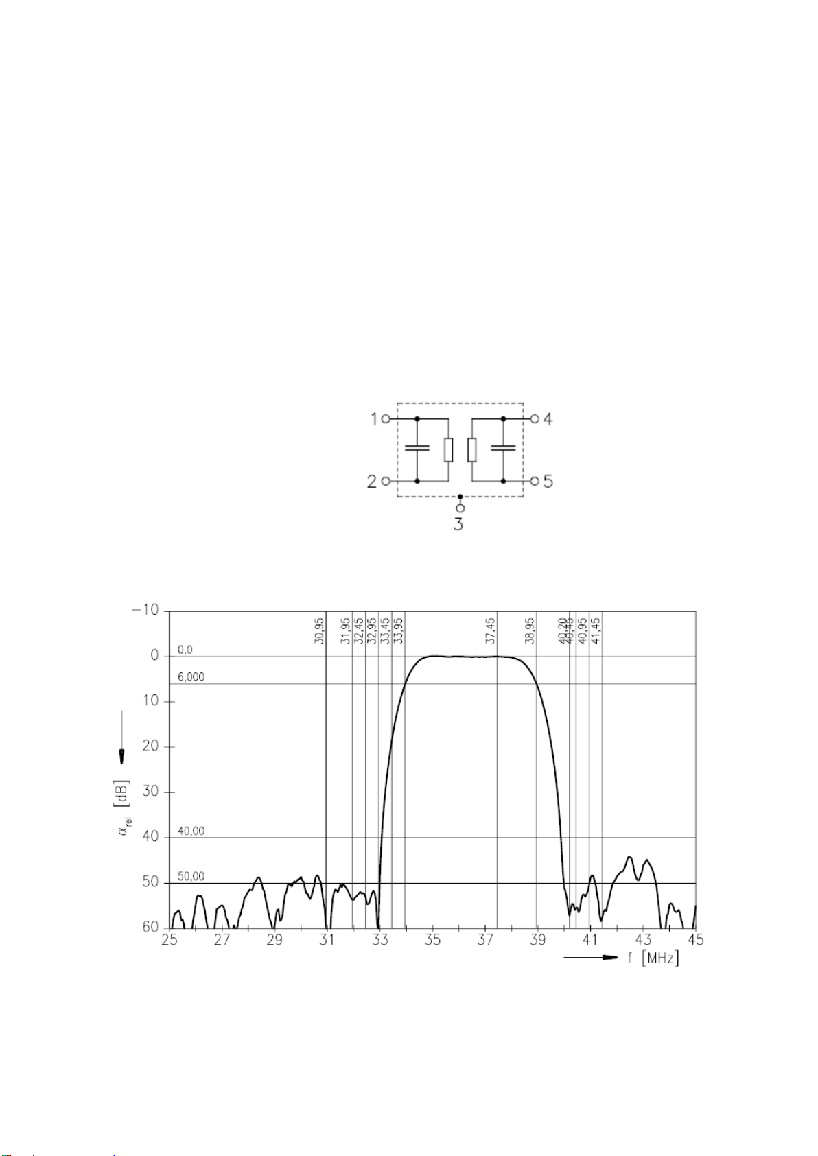
x TV IF filter with Nyquist slopes at 33.90 MHz and 38.90 MHz
x Constant group delay
3.2.3 Pin Configuration
1 Input
2 Input - ground
3 Chip - carrier ground
4 Output
5 Output
3.2.4 Frequency Response
9
Page 10
4 AUDIO AMPLIFIER STAGE WITH PT2333
4.1 General Description of PT2333:
The PT2333 is a Class-D power amplifier designed for audio equipments, maximum
output power can reach up to 2.5W (VDD=5V5/ ȍ7+' 7KH37FRPSRVHG
of exclusively designed Class-D circuitry (patented) by PTC, along with the most advanced
semi-conductor technology. When compared to the traditional Class-AB amplifiers, the
PT2333’s has a much higher efficiency (>80%), low heat dissipation, and produces superior
audio quality. PT2333’s external circuitry is simple and easily accessible, and consists of
flawless self-protection capabilities. The chip’s packaging is small, thus it occupies an
insignificant amount of space on the circuit board; therefore, making it the predominant
choice when it comes to audio amplifiers.
4.2 Features of PT2333:
• CMOS technology
• Operating voltage range from 2.7V up to 5.5V
• Differential analog input
• Maximum outSXWSRZHU:ȍ#7+'
• Output low-pass LC filter is not required.
• Voltage gain determinate by the external resister
• Contains shutdown function
• POP noises free in shutdown and power ON/OFF period
• Built-in short circuit protection
• Built-in overheat protection
10
Page 11
+LJKHIILFLHQF\ȍORDG!ORZKHDWGLVVLSDWLRQ
• Available in MSOP 10-pin and WLCSP 9-pin miniature packages
4.3 Pin Configuration of PT2333:
WLCSP-9 PACKAGE:
5 MICROCONTROLLER (MSTAR)
5.1 Genaral Description
The MST9WB6JS is a high performance and fully integrated IC for multi-function LCD
monitor/TV with resolutions up to UXGA (1600*1200)/WSXGA+ (1680*1050). It is
configured with an integrated DVI/HDCP/HDMI receiver, a multi standard TV video and
audio decoder, a video deinterlacer, a scaling engine, the MSTARACE-3 color engine, an onscreen display controller and a built in output panel interface. By use of external frame buffer,
PIP/POP is provided for multimedia applications. Furthermore, 3D video decoding and
processing are fulfilled for high-quality TV applications. To further reduce system costs, the
MST9WB6JS also integrates intelligent power management control capability for green-mode
requirements and spread spectrum support for EMI management.
11
Page 12

5.2 Features
x Single Display LCD TV controller with PC
& multimedia display functions
x Input supports up to UXGA & 1080p
x Panel supports up to UXGA (1600x1200) /
WSXGA+ (1680x1050)
x TV decoder with comb filter
x Multi-standard TV sound demodulator and
decoder
x 10-bit triple-ADC for TV and RGB/YPbP
x 10-bit video data processing
x Integrated DVI/HDCP/HDMI compliant
receiver
x High-quality dual scaling engines & dual 2-
D video de-interlacers
x 3-D video noise reduction
x MStarACE-3 picture/color processing
engine
x Embedded On-Screen Display (OSD)
controller engine
x Built-in MCU supports PWM & GPIO
x Built-in dual-link 8-bit LVDS transmitter
x 5-volt tolerant inputs
x Low EMI and power saving features
x 216-pin LQFP
r
Multi-Standard TV Sound Decoding/Processing
x Supports BTSC/A2/EIA-J demodulation and
decoding
x FM Stereo & SAP demodulation
x Supports MP3 decode
x Programmable delay for audio/video
synchronisation
x Audio processing for loudspeaker channel,
including volume, balance, mute, tone and P/G
EQ
x Optional advanced surround available (Dolby
2
SRS
, BBE3 …etc) Note
1
,
Digital Audio Interface
2
S digital audio input & output
x I
x S/PDIF digital audio output
x HDMI audio channel processing capability
x Audio Line-In L/R x2
x Audio Line-Out L/R x3
x Built-in audio DAC L/R x3
x Built-in audio ADC L/R x1
x SIF audio input
NTSC/PAL/SECAM Video Decoder
x Supports NTSC M, NTSC-J, NTSC-4.43,
PAL (B,D,G,H,M,N,I,Nc)
x Automatic TV standard detection
x 3-D Comb filter for NTSC/PAL
x 5 configurable CVBS & Y/C S-Video inputs
x Supports closed caption and V-chip
x CVBS video output
x Video IF for Multi-Standard Analog TV
x Digital low IF architecture
x Stepped-gain PGA with 26dB tuning range
and 1dB tuning resolution
x Maximum IF analog gain of 37dB in
addition to digital gain
x Programmable TOP to accommodate
different tuner gain to optimise noise and
linearity performance
Analog RGB Compliant Input Ports
x Two analog ports support up to UXGA
x Supports HDTV RGB/YPbPr/YCbCr
x Supports Composite Sync and SOG (Sync-On-
Green) separator
x Automatic color calibration
DVI/HDCP/HDMI Compliant Input Ports
x TWO DVI/HDMI input ports with built-in switch
x Supports TMDS clock up to 225MHz @ 1080P
60Hz with 12-bit deep-color resolution
x Single link on-chip DVI 1.0 compliant receiver
x High-bandwidth Digital Content Protection
(HDCP) 1.1 compliant receiver
x High Definition Multimedia Interface (HDMI) 1.3
compliant receiver with CEC support
x Long-cable tolerant robust receiver
x Supports HDTV up to 1080P
12
Page 13
6 INTEGRATED DVB-T RECEIVER (CHEERTEK)
6.1 General Description
CT216T is a highly integrated single chip for DVB-T compliant STB solution. Compared
with Cheertek's previous generations of STB receiver devices. CT216T further interates
COFDM demodulator USB 2.0 HS host controller, memory card reader, 1/2-bit SPIFlash
interface, audio DAC, PWM in/out and SAR-ADC functions. In additiont special
enhangements are provided such as MPEG-4 video decoding, 16-bit OSD with anti-flickering,
HW JPEG decoding, flesh tone and black-white extensions, and improvement of small video
quality.
CT216T includes COFDM demodulator transport stream de-multiplexer, DVB-CSA
compliant de-scrambler, RISC MPUs, MPEG-1/2/4 AV decoder, digital T\/ encoder, audio
DACs, USB 2.0 HS host controller, memory card reader, smart card reader, CI controller and
other peripherals.
Cli216T is designed in focus on the market of single tuner input product which makes, it a
cost effective solution. Supports include free to air, conditional access for SC (Smart card)
and CI portable devices, PVR, LCD TV, and other DVB-T applications.
Digital Front End Diagram:
6.2 Features
COFDM Demodulator
x ETSI EN 300 744 DVB-T NorDig Unified 1.0.3, and D-book compliant
x Automatic spectral inversion, detection
x Integrated ADC
x Direct IF (36.167 MHz or 43.75 MHz) or low IF (4.57 MHz) supported
x 6LQJOH,)$*&RUGXDO5)O)$*&FRQWUROVZLWKǻȈPRGXODERQ
x Impulsive noise cancellation
x Carrier acquisition range: ±400 kHz (extensible to ±600 kHz in 8MHz BW)
13
Page 14

x Adjacent channel interference (ACI) filter,for supporting 6, 7, and 8MHz channels
with one 8MHz analog filter
x Co-channel interterence (CCl) supression
x RF signal strength monitor
MPU
x Three 32-bit RISC MPU run up to 166MHz with total 448DMIPS
x 8KB I-Cache and 8KB D-Cache
x Two general purpose timers
x Watchdog timer
x DSU for source level debug
Memory
x 6-bit SDRAM controller supports up to 32MB (16MB for l28-pin)
x Unified memory architecture
x Parallel flash (216-pin only)
x 1/2-bit SPI flash
Transport De-multiplexing
x TS, PES, and ES demultiplexing
x OneTS path
x CI CAM interface (216-pin only)
x 32 general purpose PID filters
x 32 Section filters
x CRC-32 accelerator
x DVB-CSA de-scramblers
Video Decoding and Processing
x MPEG-2 MP@ML
x MPEG-4 SP&ASP
x PAL/NTSC format conversion
x 3:2 pull down
x Zoom in/out from 1/16X to 16X
x HW JPEG decode
x 4/8/16-bit OSD with anti-flickering
x On chip NTSC/PAL TV encoder
x CVBS, S-VHS, and component video
x VBI insertion for Teletext, CC and WSS
x ITU-R BT.601 and ITU-R BT.656 outputs
x Flesh tone extension
x Black/white extension,
Audio Decoding and Processing
x MPEG-1: layer 1/2/3
x MPEG-2: layer 1/2
x Decode MPEG-2 and MPEG-1 audio at sampling frequency of 16K, 22.05K, 24K,
32K, 44.1K, and 48KHz
x Decode CU-DA at sampling frequency of 44.1 KHz
14
Page 15

x SPDIF out for AC-3 by-pass
x Embedded 2 channels audio DAC for L/R outputs
x Digital mute control and volume adjustment
OSD(On Screen Display)
x There are total 9 display planes: border; background. video. RS1 (Rectangle Strip 1),
RS2, OSD, RS3, RS4, and cursor.
x 4/8l16-bit OSD with anti-flickering and anti-flutter
x Support alpha-blending per color
x Adjustable brightness control in window
x Bitmap OSD
x Support horizontal pixel duplication to enlarge bitmap automatically
x Support sub-region redraw to facilitate bitmap display.
Digitnal TV Encoder
x NTSC-M, PAL-B, D, G, H, I, Nc, M encoding
x Four video DACs to provide 6 configuration output: modes
x Support CVBS, S-VHS. and component video outs
x VBI insertion for Teletext, CC and WSS
x Color burst amplitude control
x Programmable sync. level
x On chip, color-bar generator
High Speed I/O
x USB 2.0 HS host controller
x Memory card reader with SD, MMC, and MS interfaces
x Compliant with SD spec. 1.1 and MMC spec. 4.0 with 1-bit & 4-bit modes.
x Compliant with Memory Stick Pro format spec. 1.02 and Memory stick format spec
1.43 with 1-bit and 4-bit modes.
Peripherals
x Up to 3 full duplex UART with 16-byte FIFO
x 2-wire serial (2WS) in master mode .. .
x Up to 2 IS0-7816 compliant SC (1 in 128-pin, can also be used as UART)
x 5 digits 7-Segrnent LED control
x 5x3 two-dimension key scan
x 2 SAR-ADC input
x 4 PWM input/output
x 1 HW IR command decode
x GPIO
Electrical and Physical Characteristics
x Capable of using single 27MHz clock input crystal
x 1.8V and 3.3V dual power supply
x Power standby mode
x PQFP-128 (CT216T-Z) or LQFP-216 (CT216T-R) package
15
Page 16

7. 4MX16 BIT SYNCHRONOUS DRAM ( DIGITAL SIDE
SDRAM)
7.1 General Description
The EM638165 SDRAM is a high-speed CMOS synchronous DRAM containing 64 Mbits. It
is internally configured as 4 Banks of 1M word x 16 DRAM with a synchronous interface (all
signals are registered on the positive edge of the clock signal, CLK). Read and write accesses
to the SDRAM are burst oriented; accesses start at a selected location and continue for a
programmed number of locations in a programmed sequence. Accesses begin with the
registration of a BankActivate command which is then followed by a Read or Write
command. The EM638165 provides for programmable Read or Write burst lengths of 1, 2, 4,
8, or full page, with a burst termination option. An auto precharge function may be enabled to
provide a self-timed row precharge that is initiated at the end of the burst sequence. The
refresh functions, either Auto or Self Refresh are easy to use. By having a programmable
mode register, the system can choose the most suitable modes to maximize its performance.
These devices are well suited for applications requiring high memory bandwidth and
particularly well suited to high performance PC applications.
7.2 Features
x Fast access time from clock: 4.5/5/5.4 ns
x Fast clock rate: 200/166/143 MHz
x Fully synchronous operation
x Internal pipelined architecture
x 1M word x 16-bit x 4-bank
x Programmable Mode registers
x CAS Latency: 2, or 3
x Burst Length: 1, 2, 4, 8, or full page
x Burst Type: interleaved or linear burst
x Burst stop function
x Auto Refresh and Self Refresh
x 4096 refresh cycles/64ms
x CKE power down mode
x Single +3.3V ± 0.3V power supply
x Interface: LVTTL
x 54-pin 400 mil plastic TSOP II package
x Pb free and Halogen free
x 60-ball 6.4mm x 10.1mm VFBGA package
x Pb free
16
Page 17
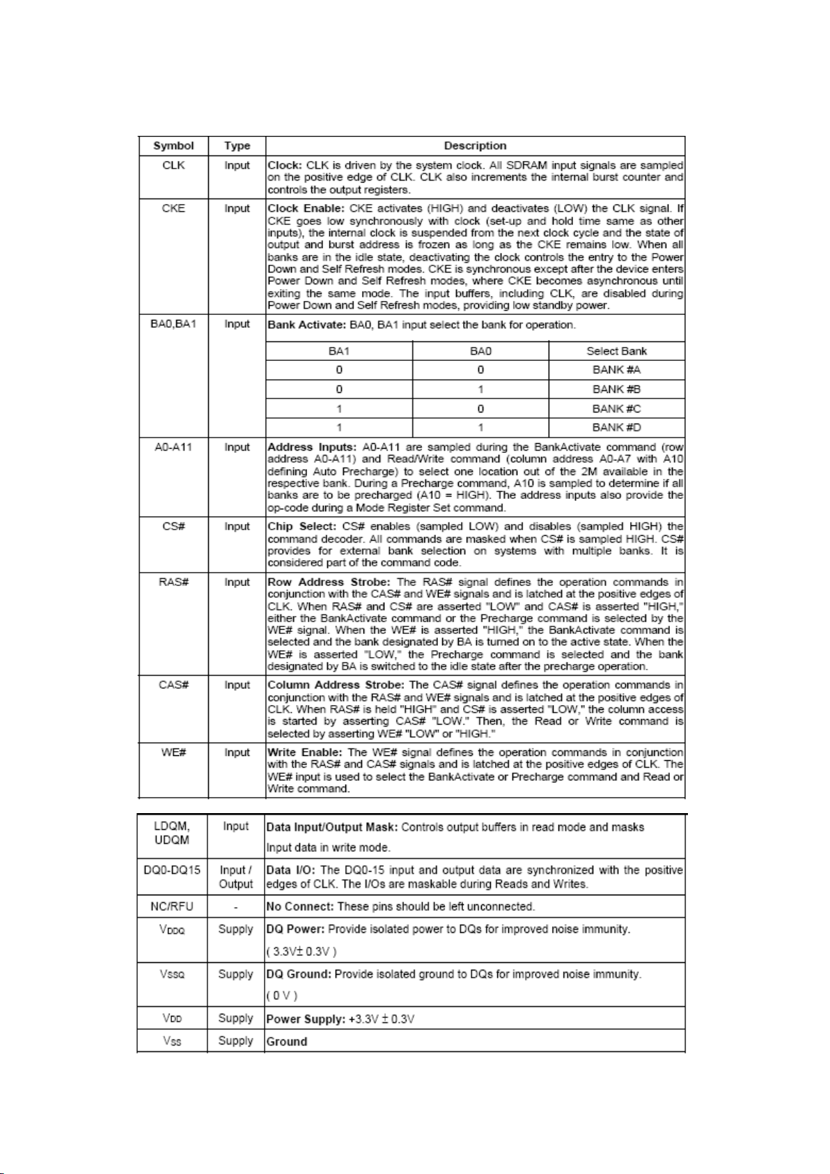
7.3 Pin Configuration
17
Page 18

8 S25FL016A - 16 Megabit Cmos 3.0 Volt Flash Memory with
50-Mhz (Serial Peripheral Interface)Bus
8.1 General Description
The S25FL016A is a 3.0 Volt (2.7V to 3.6V), single-power supply Flash memory device.The
device consist of thirty-two sectors, each with 512 Kb memory.
The device accepts data written to SI (Serial Input) and outputs data on SO (Serial Output).
The devices are designed to be programmed in-system with the standart 3.0 volt Vcc supply.
The memory can be programmed 1 to 256 bytes at a time, using the Page Praogram
command. The device supports Sector Erase and Bulk Erase commands.
Each device requires only a 3.0 volt power supply (2.7V to 3.6V) for both read and write
functions. Internally generated and regulated voltages are provided for the program
oprerations. This device does not require a Vpp supply.
8.2 Distinctive Characteristics
Architectural Advantages
x Single Power supply operation
- Full voltage range: 2,7 to 3,6V read and program operations
x Memory Architecture
- Thirty-two sectors with 512 Kb each
x Program
- Page program (up to 256 bytes) in 1,4 ms (typical)
- Program operations are on a page by page basis
x Erase
- 0,5s typical sector erase time
- 10s typical bulk erase time
x Cycling Endurance
- 100,000 cycles per sector typical
18
Page 19

x Data Retantion
- 20 Years Typical
x Device ID
- JEDEC standart two-byte electronic signature
- RES command one-byte electronic signature for backward compatibility
x Process Technology
- Manufactured on 0,20 μm MirrorBit process technology
x Package Option
- Industry standart pinout
- 16-pin SO package (300 mils)
- 8-pin SO package (208 mils)
- 8-Contact WSON Package (6x8 mm), Pb Free
Performance Characteristics
x Speed
- 50Mhz clock rate (miximum)
x Power Saving Standby Mode
- Standby Mode 50 μA (max)
- Deep Power Down Mode 1,3μA (typical)
Memory Protection Features
x Memory Protection
- W# pin works in conjuction with Status Register Bits to protect specified memory
areas
- Status Register Block Protection bits (BP2, BP1, BP0) in status register configure
parts of memory as read-only
Software Features
SPI Bus Compatible Serial Interface
19
Page 20

9 4M x 16 bit Synchronous DRAM (ANALOG SIDE SDRAM)
9.1 General Description
The EM638165 SDRAM is a high-speed CMOS synchronous DRAM containing 64Mbits. It
is internally configured as 4 Banks of 1M word x 16 DRAM with a synchronous interface (all
signals are registered on the positive edge of the clock signal, CLK). Read and write accesses
to the SDRAM are burst oriented; accesses start at a selected location and continue for a
programmed number of locations in a programmed sequence. Accesses begin with the
registration of a Bank Activate command which is then followed by a Read or Write
command. The EM638165 provides for programmable Read or Write burst lengths of 1, 2, 4,
8, or full page, with a burst termination option. An auto precharge function may be enabled
to provide a self-timed row precharge that is initiated at the end of the burst sequence. The
refresh functions, either Auto or Self Refresh are easy to use. By having a programmable
mode register, the system can choose the most suitable modes to maximize its performance.
These devices are well suited for applications requiring high memory bandwidth and
particularly well suited to high performance PC applications.
9.2 Features
• Fast access time from clock: 4.5/5/5.4 ns
• Fast clock rate: 200/166/143 MHz
• Fully synchronous operation
• Internal pipelined architecture
• 1M word x 16-bit x 4-bank
• Programmable Mode registers
- CAS Latency: 2, or 3
- Burst Length: 1, 2, 4, 8, or full page
- Burst Type: interleaved or linear burst
- Burst stop function
• Auto Refresh and Self Refresh
• 4096 refresh cycles/64ms
• CKE power down mode
• Single +3.3V ± 0.3V power supply
• Interface: LVTTL
• 54-pin 400 mil plastic TSOP II package
- Pb free and Halogen free
• 60-ball 6.4mm x 10.1mm VFBGA package
- Pb free
20
Page 21

9.3 Pinning
21
Page 22

10 POWER STAGE
MB45 has two power options which is changed according to TV size and number of lambs.
10.1 IPS 15 Option
IPS16 power board is used with 19” MB45TV set (2 lamp panel) and IPS17 power board is
used with 22” MB45TV set (4 lamp panel). These are supplied 12V, 5V_stby and 5V panel
supplies.
Also regulators, step-downs and mosfet generate 3V3, 3V3_Stby, 5V_Tuner and 1,25V_Stby
voltages for other different part of the chassis.
Audio supply is 5V in this case.
22
Page 23

11 IC SPECIFICATIONS
11.1 8K Smart Serial EEPROM – 24C64
General Description
24C64 is a 64Kbit CMOS non-volatile serial EEPROM organized as 8K x 8 bit memory. This
device confirms to Extended IIC 2-wire protocol that allows accessing of memory in excess
of 16Kbit on an IIC bus. This serial communication protocol uses a Clock signal (SCL) and a
Data signal (SDA) to synchronously clock data between a master (e.g. a microcontroller) and
a slave (EEPROM). 24C64 is designed to minimize pin count and
simplify PC board layout requirements.
24C64 offers hardware write protection where by the entire memory array can be write
protected by connecting WP pin to VCC. This section of memory then becomes unalterable
until the WP pin is switched to VSS.
Features
([WHQGHGRSHUDWLQJYROWDJH9WR9
8SWR.+]FORFNIUHTXHQF\DW9WR9
/RZSRZHUFRQVXPSWLRQ
—0.5mA active current typical
—ȝ$VWDQGE\Furrent typical
—ȝ$VWDQGE\FXUUHQWW\SLFDO/YHUVLRQ
—ȝ$VWDQGE\FXUUHQWW\SLFDO/=YHUVLRQ
6FKPLWWWULJJHULQSXWV
E\WHSDJHZULWHPRGH
6HOIWLPHGZULWHF\FOHPVW\SLFDO
+DUGZDUH:ULWH3URWHFWLRQIRUWKHHQWLUHDUUD\
(QGXUDQFHXSWo 100K data changes
'DWD5HWHQWLRQ*UHDWHUWKDQ\HDUV
3DFNDJHV-Pin DIP, 8-Pin SO and 8-Pin TSSOP
7HPSHUDWXUHUDQJH
—Commercial: 0°C to +70°C
—Industrial (E): -40°C to +85°C
—Automotive (V): -40°C to +125°C
Pin Configuration
23
Page 24

11.2 TL062
It is used as a pre-amplifer for scart audio output on MB45 main board.
General Description
Low-power JFET-input operational amplifier
Features
x Very Low Power Consumption
x Typical Supply Current . . . 200 μA (Per Amplifier)
x Wide Common-Mode and Differential Voltage Ranges
x Low Input Bias and Offset Currents
x Common-Mode Input Voltage Range Includes VCC+
x Output Short-Circuit Protection
x High Input Impedance . . . JFET-Input Stage
x Internal Frequency Compensation
x Latch-Up-Free Operation
x High Slew Rate . . . 3.5 V/μs Typ
Pin Configuration
24
Page 25

11.3 FSA3157
It is used for switching DVD_Y/C video signal and DVB_Y/C video signal on the MB45
mainboard, also there are two jumpers option for by-passing this switch.
General Description
FSA3157 is a high performance, single-pole/double-throw (SPDT) Analog Switch or 2:1
Multiplexer/Demultiplexer Bus Switch. The device is fabricated with advanced sub-micron
CMOS technology to achieve high speed enable and disable times and low On Resistance.
The break before make select circuitry prevents disruption of signals on the B Port due to both
switches temporarily being enabled during select pin switching. The device is specified to
operate over the 1.65 to 5.5V VCC operating range. The control input tolerates voltages up to
5.5V independent of the VCC operating range.
Features
_ Useful in both analog and digital applications
_ Space saving SC70 6-lead surface mount package
_ Ultra small MicroPakOHDGOHVVSDFNDJH
B/RZ2Q5HVLVWDQFHȍRQW\S#99&&
_ Broad VCC operating range; 1.65V to 5.5V
_ Rail-to-Rail signal handling
_ Power down high impedance control input
_ Overvoltage tolerance of control input to 7.0V
_ Break before make enable circuitry
_ 250 MHz - 3dB bandwidth
Pin Configuration
25
Page 26

11.4 FDS8878
It is used for providing 5V tuner supply.
General Description
This N-Channel MOSFET has been designed specifically to improve the overall efficiency of
DC/DC converters using either synchronous or conventional switching PWM controllers. It
has been optimized for low gate charge, low rDS(on) and fast switching speed.
Features
U'6RQ Pȍ9*6 9,' $
U'6RQ Pȍ9*6 9,' $
High performance trench technology for extremely low rDS(on)
Low gate charge
High power and current handling capability
RoHS Compliant
Pin Configuration
11.5 ST24LC21 (Optional)
ST24LC21 is an EEPROM which is used for storing the VGA output resolution information.
General Description
The ST24LC21 is a 1K bit electrically erasable programmable memory (EEPROM),
organized by 8 Bits.This device can operate in two modes: Transmit Only mode and I2C
bidirectional mode. When powered, the device is in Transmit Only mode with EEPROM data
clocked out from the rising edge of the signal applied on VCLK. The device will switch to the
I2C bidirectional mode upon the falling edge of the signal applied on SCL pin. The
ST24LC21 cannot switch from the I2C bidirectional mode to the Transmit Only mode (except
when the power supply is removed). The device operates with a power supply value as low as
2.5V. Both Plastic Dual-in-Line and Plastic Small Outline packages are available.
26
Page 27

Features
x 0ÕOOÕRQ(UDVH:UÕWH&\FOHV
x <HDUV'DWD5HWHQWÕRQ
x Y7RY6ÕQJOH6XSSO\9ROWDJH
x N+]&RPSDWÕEÕOÕW\2YHU7KH)XOO
x Range Of Supply Voltage
x 7ZR:ÕUH6HUÕDO,QWHUIDFH,F%XV
x &RPSDWÕEOH
x 3DJH:UÕWH8S7R%\WHV
x %\WH5DQGRP$QG6HTXHQWÕDO5HDG
x Modes
x 6HOI7ÕPHG3URJUDPPÕQJ&\FOH
x $XWRPDWÕF$GGUHVV,QFUHPHQWÕQJ
x Enhanced Esd/Latch Up
x Performances
Pin Configuration
11.6 TDA1308T
TDA1308T is a class AB stereo headphone driver which is used as a headphone amplifier on
MB45 mainboard.
General Description
The TDA1308 is an integrated class AB stereo headphone driver contained in an SO8, DIP8
or a TSSOP8 plastic package. The device is fabricated in a 1 mmCMOS process and has been
primarily developed for portable digital audio applications.
Features
· Wide temperature range
· No switch ON/OFF clicks
· Excellent power supply ripple rejection
27
Page 28

· Low power consumption
· Short-circuit resistant
· High performance
– high signal-to-noise ratio
– high slew rate
– low distortion
· Large output voltage swing.
Pin Configuration
11.7 STMP2161
STMP2161 is a current limiter which is used for switching the USB interface on MB45
mainboard.
General Description
The STMPS2161 power distribution switches are intended for applications where heavy
capacitive loads and short circuits are likely to be encountered. These devices incorporate 90
Pȍ1-channel MOSFET high-side power switches for power-distribution. These switches are
controlled by a logic enable input.
28
Page 29

When the output load exceeds the current-limit threshold or a short is present, the device
limits the output current to a safe level by switching into a constant-current mode. When
continuous heavy overloads and short circuits increase the power dissipation in the switch,
causing the junction temperature to rise, a thermal protection circuit shuts the switch off to
prevent damage. Recovery from a thermal shutdown is automatic once the device has cooled
sufficiently. Internal circuitry ensures the switch remains off until a valid input voltage is
present.
Features
ŶPȍKLJK-side MOSFET switch
ŶP$FRQWLQXRXVFXUUHQW
Ŷ7KHUPDODQGVKRUW-circuit protection with
overcurrent logic output
Ŷ2SHUDWLQJUDQJHIURP9WR9
Ŷ&026- and TTL-compatible enable inputs
Ŷ8QGHUYROWDJHORFNRXW89/2
Ŷȝ$PD[LPum standby supply current
Ŷ$PELHQWWHPSHUDWXUHUDQJH-40°C to 85°C
ŶN9(6'SURWHFWLRQ
Ŷ5HYHUVHFXUUHQWSURWHFWLRQ
Ŷ)DXOW-blanking
Pin Configuration
29
Page 30

11.8 AZ1045
It is used for protecting the USB interface on MB45 mainboard.
General Description
AZ1045-04SU is a design which includes ESD rated diode arrays to protect high speed data
interfaces. The AZ1045-04SU has been specifically designed to protect sensitive components
which are connected to data and transmission lines from over-voltage caused by Electrostatic
Discharging (ESD).
AZ1045-04SU is a unique design which includes ESD rated, ultra low capacitance steering
diodes and a unique design of clamping cell which is an equivalent TVS diode in a single
package. During transient conditions, the steering diodes direct the transient to either the
power supply line or to ground line. The internal unique design of clamping cell prevents
over-voltage on the power line, protecting any downstream components. Besides, there is a
back-drive protection design in AZ1045-04SU for power-down mode operation. AZ104504SU may be used to meet the ESD immunity requirements of IEC 61000-4-2, Level 4
(±15kV air, ±8kV contact discharge).
Features
ESD Protect for Transition Minimized Differential Signaling (TMDS) channels
Protects four I/O lines and one VDD line
Provide ESD protection for each channel to
Revision 2008/01/23 ©2008 Amazing Micro. 1 www.amazingIC.com
IEC 61000-4-2,(ESD) ±15kV (air), ±8kV (contact)
IEC 61000-4-/LJKWQLQJ$ȝV
For below 5V operating voltage
Ultra low capacitance : 0.55pF typical
0.03pF matching capacitance between the TMDS intra-pair
Fast turn-on and Low clamping voltage
Array of ESD rated diodes with internal equivalent TVS diode
30
Page 31

Solid-state silicon-avalanche and active circuit triggering technology
Back-drive protection for power-down mode
Lead-free version available
Pin Configuration
11.9 MP1583
MP1583 is a step-down regulator which is used for providing 3.3V DC from 12V DC and 5V
Vcc from 12V.
General Description
The MP1583 is a step-down regulator with a built in internal Power MOSFET. It achieves 3A
continuous output current over a wide input supply range with excellent load and line
regulation. Current mode operation provides fast transient response and eases loop
stabilization. Fault condition protection includes cycle-by-cycle current limiting and thermal
shutdown. Adjustable soft-start reduces the stress on the input source at turn-on. In shutdown
mode the regulator draws 20μA of supply current.
The MP1583 requires a minimum number of readily available external components to
complete a 3A step down DC to DC converter solution.
31
Page 32

Features
x 3A Output Current
x Programmable Soft-Start
x 100m,QWHUQDO3RZHU026)(76ZLWFK
x Stable with Low ESR Output Ceramic Capacitors
x Up to 95% Efficiency
x 20μA Shutdown Mode
x Fixed 385KHz frequency
x Thermal Shutdown
x Cycle-by-Cycle Over Current Protection
x Wide 4.75 to 23V operating Input Range
x Output Adjustable From 1.22 to 21V
x Under Voltage Lockout
x Available in 8 pin SOIC Package
x 3A Evaluation Board Available
Pin Configuration
32
Page 33

11.10 LM1117
It is a regulator which is used for providing 1.8V from 3.3V for DVB side.
General Description
The LM1117 is a series of low dropout voltage regulators with a dropout of 1.2V at 800mA of
load current. It has the same pin-out as National Semiconductor’s industry standard LM317.
The LM1117 is available in an adjustable version, which can set the output voltage from
1.25V to 13.8V with only two external resistors. In addition, it is also available in five fixed
voltages, 1.8V, 2.5V, 2.85V, 3.3V, and 5V. The LM1117 offers current limiting and thermal
shutdown. Its circuit includes a zener trimmed bandgap reference to as-sure output voltage
accuracy to within ±1%. The LM1117 series is available in SOT- 223, TO-220, and TO-252
D-PAKSDFNDJHV$PLQLPXPRIȝ)WDQWDOXPFDSDFLWRULVUHTXLUHGDWWKHRXWSXWWRLPSURYH
the transient response and stability.
Features
x Available in 1.8V, 2.5V, 2.85V, 3.3V, 5V, and Adjustable Versions
x Space Saving SOT-223 Package
x Current Limiting and Thermal Protection
x Output Current 800mA
x Line Regulation 0.2% (Max)
x Load Regulation 0.4% (Max)
x Temperature Range
x LM1117 0°C to 125°C
x LM1117I -40°C to 125°C
Pin Configuration
33
Page 34

11.11 MP2109
It is a step-down converter which is used for setting the 1.26V STBY Output and 3.3V STBY
Output.
General Description
The MP2109 contains two independent 1.2MHz constant frequency, current mode, PWM
step-down converters. Each converter integrates a main switch and a synchronous rectifier for
high efficiency without an external Schottky diode. The MP2109 is ideal for powering
portable equipment that runs from a single cell Lithium-Ion (Li+) battery. Each converter can
supply 800mA of load current from a 2.5V to 6V input voltage. The output voltage can be
regulated as low as 0.6V. The MP2109 can also run at 100% duty cycle for low dropout
applications.
Features
Up to 95% Efficiency
1.2MHz Constant Switching Frequency
800mA Load Current on Each Channel
2.5V to 6V Input Voltage Range
Output Voltage as Low as 0.6V
100% Duty Cycle in Dropout
Current Mode Control
Short Circuit Protection
Thermal Fault Protection
ȝ$6KXWGRZQ&XUUHQW
Internally Compensated
Space Saving 10-Pin QFN Package
Pin Configuration
34
Page 35

11.12 FDC642P
FDC642P is a p-channel mosfet which is used for switching the panel supply.
General Description
This P-channel 2.5V specified MOSFET is produced using advanced PowerTrench process
that has been especially tailored to minimize on state resistance and yet maintain low gate
charge for superior switching performance.
These devices have been design to offer exceptional power dissipation in a very small
footprint for applications where larger packages are impractical.
Features
x Fast switching speed.
x -4 A,-20V. RDS(on) = 0.065 ohm @ VGS=-4.5V
RDS(on) = 0.100 ohm @ VGS=-2.5V
x Low gate charge (7.2nC typical).
x High performance trench technology for extremely low RDS(on)
x SuperSOT-6 package:small footprint (72% smaller than Standard SO-8;low profile
(1mm thick).
35
Page 36

Pin Configuration
11.13 XC5000 (Optional)
XC50000 is a RF to Baseband Silicon Tuner and the usage of XC5000 is optional on
MB45TV set.
General Description
The Single-Chip Multi-Standard Tuner + VIF/SIF XC5000 supports all analog TV formats
transmitted worldwide in the 42-864 MHz band on either cable or terrestrial broadcast
channels. It implements on-chip tuning, channel filtering and demodulation, without external
(SAW) filters and has no manually tunable parts. The broadband tuner converts the selected
channel into an Intermediate Frequency (IF), which is then sampled by an internal highresolution analog-to-digital converter (A/D) for further processing. For analog broadcast
standards the video signal is demodulated and output as a composite video base-band signal
(CVBS) through a high-performance smoothing filter. The sound carrier is filtered and output
as a 2nd Sound IF (SIF) or demodulated and output as a mono TV sound. In DTV mode, the
Digital TV signals are filtered using a standard-dependent high-rejection channel fitler and
converted to a user-programmable output frequency. At the output of the D/A converter, the
DTV signal is low-pass filtered using a high-performance smoothing filter and input to a
variable gain amplifier. The amplifier gain can be controlled via an external analog signal on
Vagc.
Features
_ Standard specific digital picture carrier recovery:
Alignment-free
Quartz-stable and accurate
No externally tunable parts
_ Multi-standard RF-to-baseband receiver
_ Integrated RF PLL filter reducing risk of noise pickup on the board
_ Standard specific digital video/audio splitting
_ Integrated DSP for high quality demodulation both in analog and digital modes
_ Integrated smoothing filters for CVBS output (analog mode) and IF-output (digital mode)
_ Supports DDI (digital direct interface) interfacing to the digital demodulator equipped with
DDI, eliminating the quantization noise (from DAC/ADC).
_ Onboard digital processing for the following analog standards: B/G, D/K, I, L/L’ and M/N
_ Inter-carrier sound output or mono analog sound direct output
36
Page 37

_ Mono analog sound demodulation for both AM (SECAM L/L') and FM, including de
emphasis
_ Compatible with a wide variety of signal conditions, including video overmodulation,
airplane flutter and nonstandard sound.
_ DTV Mode for operation with external DTV demodulator. XC5000 applies filters and
converts signal to arbitrary output frequency. Supports standards such as ATSC, OpenCable,
DVB-C, DVB-T, ISDB-T, DMB-TH.
_ Excellent adjacent channel rejection
_ Low noise and excellent SNR
_ Dual input capability to address both TV and FM radio reception
_ Controlled via I2C-bus, up to four units on the I2C bus via address select pin
_ 42 to 864 MHz input frequency range
_ Low power dissipation
_ Small footprint, QFN48
_ Lead-free manufacturing
The Single-Chip Multi-Standard Tuner plus VIF/SIF, XC5000 combines both tuning and
demodulation functions for worldwide cable and terrestrial analog TV in one small package.
It also includes high performance filtering and frequency-conversion functions for DTV with
an external demodulator through LOW-IF or DDI. The XC5000’s integrated tuner is based on
proprietary tunable wideband active RF filtering technology that eliminates the need for
special external components. The XC5000’s high sensitivity, coupled with at least 65 dB
image rejection makes it ideal for antenna and cable reception. The XC5000’s integrated
digital demodulation for analog TV performs the entire multi-standard Quasi Split Sound
(QSS) TV IF processing, AGC, video demodulation, generation of the 2nd sound IF (SIF) or
mono TV sound for all worldwide standards. The XC5000 provides two inputs to address
both TV and FM radio reception. Xceive's breakthrough patent-pending technology provides
a powerful combination of high dynamic range with a large tunable range uniquely enabling
superior pictures from off-air and cable applications. Supported formats include NTSC, PAL
and SECAM. The XC5000 also supports most DTV standards including ATSC/8-VSB,
OpenCable DVB-C, QAM64 & QAM256, DVB-T, ISDB-T and DBM-TH, and is compatible
with most digital demodulators on the market today.
Pin Configuration
37
Page 38

38
Page 39

12 BLOCK DIAGRAMS
12.1 General Block Diagram
Page 40

THIS PAGE INTENTIONALLY
LEFT BLANK
Page 41

12.2 Integrated DVB-T Receiver Block Diagram
Page 42

12.3 17MB45 Analog Front-End
12.4 17MB45 Digital Front-End
42
Page 43

12.5 17MB45 Digital CI ve Smart Card Interface
12.6 17MB45 HDMI Inputs
43
Page 44

12.7 17MB45 Analog Interface “ MSTAR IC “
Page 45

12.8 17MB45 Analog Input / Output
12.9 17MB45 LVDS Output
Page 46

12.10 17MB45 Power
46
Page 47

12345678
5V_TUN
5V_TUN
A
B
C
D
E
F
SC101
LG
IF_AGC
TU101 TDTC-G101D
RF_AGC
ANT_PWR
5V_TUN
21
20
19
18
17
16
15
14
13
12
11
SCART LT1
10
9
8
7
6
5
4
3
2
1
AIF
DIF1
DIF2
SDA
SCL
ANALOG_IF
C140
C139
220n
10V
F102
600R
21
R136
321
DIGITAL_IF_N
50V
47p
DIGITAL_IF_P
IF_AGC_DVB
C141
220n
10V
21
1k
0R
5V_TUN
NUP4004M5
D107
5
4
C110
50V
3n3
F103
600R
21
RF_AGC
5V_VCC
12V_VCC
50V
R116
100R
C112
4n7
50V
5V_VCC
220p
C113
C111
3n3
21
21
50V
21
SDA_TUNER
R137
100R
8
R1
7
R2
6
R3
54
R4
SCL_TUNER
R791
1k
21
50V
C114
220p
R117
220R
F104
21
600R
F105
21
600R
SC1_AUD_R_IN
SC1_AUD_R_OUT
12V_VCC
1
SDA_TUN_DVB
2
SDA
3
SCL_TUN_DVB
SCL
Q1
8
FDS8878
1
72
6
3
54
BSH103
Q716
21
TL431SAMF2
21
U707
C787
1n
50V
R790
21
R792
1k
1k
C117
SC1_CVBS_IN
50V
220p
21
C115
1n
50V
47R
21
R122
SC1_R
75R
21
R121
50V
220p
21
C118
75R
21
R120
R119
21
22k
D108
21
C15V
SC1_B
R123
4k7
C119
21
100n
10V
SC1_AUD_L_IN
R118
21
100R
SC1_AUD_L_OUT
C116
4n7
50V
R138
1k
R139
1k
ANALOG_IF
F722
21
330R
SC1_CVBS_OUT
SC1_FB
TX/SDA_SC
SC1_G
RX/SCL_SC
SC1_PIN8
21
F717
21
330R
1
C143
21
47u
2
16V
R141
C142
R140
56R
21
10n
16V
21
R142
5V_TUN
6V3
C135
2
1
100n
10V
100u
C138
INDIA OPTION
SC1_CVBS_IN
SCART_AUD_L_IN
SCART_AUD_R_IN
SC1_AUD_R_OUT
SC1_R_OUT
C786
1u
16V
680R
R145
L103
1u
4k7
1k
C144
2
100n
1
10V
R143
1k2
21
2
21
3
1
21
R144
Q104
BF799
10R
21
R146
1
47R
39R
2
SCART VIDEO OUTPUT AMPLIFIER
12V_VCC
4
YEL
3
WHT
2
RED
1
JK604
R124
470R
SC1_CVBS_OUT
F719
330R
SIDE AV INPUT
JK101
YEL
WHT
RED
6
5
4
3
2
1
D101
PRE-AMP for SCART
R800
20k
V+
10V
10u
21
C774
21
C778
100p
50V
R794
82k
C784
1u
16V
21
V+
10V
21
C773
10u
R798
21
33k
1
OUT1
2
IN1-
3
IN1+
L102
390nH
21
1u
12
11
10
9
AS
8
NC
7
B2
6
2
1
C136
100n
10V
5V_TUN
5
4
3
B1
2
1
2
1
C137
100n
10V
TH1
2R1
NUP4004M5
D106
5
4
321
50V
220p
21
C109
SCART_AUD_L_IN
SCART_AUD_R_IN
VSS IN2+
21
6k8
R127
C121
21
21
10n
16V
6k8
R128
SIF_CTL
C122
21
10n
16V
21
21
C120
BC858B
R125
75R
C3
10p
50V
C5V6
C102
F108
600R
F106
21
600R
33k
21
R795
R796
33k
C780
21
100n
16V
VDD
U706
OUT2
TL062
IN2-
21
3k3
R130
5V_TUN
22k
21
IN1 OUT1
2
IN2
10V
10u
1
Q102
3
SAV_CVBS
50V
21
220p
21
C101
3n3
50V
21
12V_VCC
21
8
7
6
54
V+
21
R129
R131
1
100k
Z102
K3958M
OUT2
GND
3
2
R126
300R
50V
C103
3n3
SAV_AUD_R_IN
F721
600R
C779
100p
50V
R793
82k
BA782
D109
2
1
41
5
Q101
BC848B
21
SAV_AUD_L_IN
R797
21
33k
21
SIF
IN1 OUT1
2
IN2
2
Q103
BSN20
3
21
2u2
L101
390R
R102
3
1
100R
21
12V_VCC
10V
10u
21
C775
R799
K9656M
VIFM
VIFP
R101
Z101
GND
R103
2
R104
OUT2
3
68k
33k
21
N.C.
S714
41
5
DVD/IDTV_SW
C104
21
10u
10V
SC1_AUD_L_OUT
C785
1u
16V
5V_TUN
RF_AGC
CVBS0_OUT
SC1_L_OUT20k
SIFP
SIFM
100n
CN101
10V
16V
F110
330R
22u
C125
C128
1
2
21
21
10V
10u
C123
100n
10V
C124
10u
10V
21
21
3V3_VCC
3V3_STBY
F109
330R
21
C126
21
10u
C1
2
1
6
5
43
3V3_VCC
B1
S
U1
GND
VCC
FSA3157
B0A
S4
21
1
2
F111
330R
10V
21
R133
21
12k
D110
21
1N4148
C130
100n
10V
2
1
C132
21
C129
100n
10V
2
1
21
C127
220n
10V
10V
100n
SIFP
SIFM
VIFM
VIFP
C133
R134
21
F113
21
47p
5k6
330R
U102
50V
MST9WB6JS
45
AVDD_MPLL
46
VR27
47
AVDD_RXS
48
GND_RXS
49
SIFP
50
SIFM
51
VIFM
52
VIFP
53
GND_RXV
54
AVDD_RXV
55
TAGC
C134
100n
10V
2
1
A
4
B
5V_TUN
C
VGA INPUT
5V_VCC
21
1
15
14
13
12
11
10
NUP4004M5
D103
5
4
321
R105
R106
2k2
2k2
21
21
9
VGA_DDC_5V
8
7
6
5
4
21
R110
10k
21
R113
R109
100R
21
10k
10k
R114
R115
100R
8
1
R1
7
2
R2
6
3
R3
54
R4
21
R761
R760
33R
UART0_TXD0
UART0_RXD0
C108
2
100n
1
10V
VGA_VSNC
VGA_HSNC
21
TX/SDA_SC33R
21
RX/SCL_SC
N.C.
DIGITAL SW UPDATE
3
2
1
TP101
NUP4004M5
5
4
321
C5V6
21
C105
D102
D104
27p
50V
C106
21
27p
50V
C107
21
50V
27p
PROJECT NAME :
SCH NAME :
DRAWN BY :
TUNER & PREPs
VGA_B
VGA_G
VGA_R
3
1
1
1
TP104
TP103
TP102
N.C.
17mb45-3
D105
BAV70
VGA_DDC_5V
8
VCC
7
WP
ST24LC21
6
SCL
54
U101
1
A0
2
A1
3
A2
GNDSDA
hindistan opt.
SHEET:
OF:
3-27-2008_13:22
87654321
D
1
TP105
E
F
A3
81
AX M
Page 48

12345678
DVD_C_IN
DVB_C
A
DVD_Y_IN
DVB_Y
B
VIDEO INPUTs
SW_C_IN 47R
SW_Y_IN
SAV_CVBS
C
SILICON TUNER CVBS INPUT
TUNER_CVBS
SCART RGB&CVBS
SC1_CVBS_IN
D
SC1_B
SC1_G
SC1_R
E
PC RGB&YPbPr
VGA_B
VGA_G
F
VGA_R
S201
21
1
B1
2
GND
FSA3157
B0 A
1
B1
2
GND
FSA3157
B0 A
U202
S202
S203
U203
S204
S
VCC
21
21
S
VCC
21
IDTV/DVD YC
R279
R276
270R
R277
270R
R280
47R
SAV CVBS INPUT
R219
75R
75R
R220
75R
R221
75R
R222
R223
75R
75R
R224
75R
R201
75R
R278
75R
R772
47R
R225
R226
470R
R227
47R
R228
47R
R229
47R
R230
47R
R231
47R
R232
470R
R202
47R
R281
47R
R764
47R
6
5
43
6
5
43
21
21
21
21
21
21
21
21
21
21
21
21
21
C215
47n
C216
C217
47n
C218
47n
C219
47n
C220
47n
C221
47n
C222
C201
47n
16V
1n
16V
16V
16V
16V
16V
1n
50V
16V
C238
47n
C767
47n
16V
50V
1u
C781
DVD/IDTV_SW
5V_SW
SW_C_IN
DVD/IDTV_SW
5V_SW
SW_Y_IN
5V_TUN
16V
47n
21
C239
C240
21
47n
16V
CVBS2
21
16V
CVBS0
21
CVBS1
21
SOGIN0
21
BIN0P
21
GIN0P
21
RIN0P
21
BIN1P
21
GIN1P
21
SOGIN1
21
RIN1P
21
6V3
R210
21
47R
R211
1
47R
3V3_STBY
R256
21
4k7
21
21
21
21
3V3_VCC
C236
21
27p
50V
R269
X201
C237
27p
50V
21
14.31818MHz
3V3_VCC
3V3_VCC
3V3_STBY
4k7
21
R271
3V3_STBY
DVD_SENSE
4k7
R258
4k7
R260
4k7
R262
4k7
R264
4k7
21
21
R267
R266
100R
4k7
R268
21
3V3_STBY
R209
21
4k7
R212
21
4k7
21
R272
1M
R274
21
4k7
R275
21
4k7
4k7
R270
R7
21
4k7
R4
54
R3
6
R2
7
1
TP201
R1
8
1
100R
TP202
R803
21
VDDP
R273
4k7
R218
21
4k7
47R
21
VDDP
VDDC
3
2
1
21
N.C.
43
44
73
74
75
76
77
151
152
153
154
155
158
159
160
161
162
163
165
166
170
167
168
157
169
201
200
XOUT
XIN
GPIOD[0]
GPIOD[1]
GPIOD[2]
VDDP_1
GND_7
VDDC_2
SAR0
SAR1
SAR2
SAR3
DDCR_SDA
DDCR_SCL
DDCA_SDA
DDCA_SCL
INT
IRIN
PWM2
PWM3
GND_8
VDDP_3
GPIOT[1]
POWER_CTRL
HWRESET
GPIOM[0]
GPIOM[1]
U102
MST9WB6JS
3
A
B
C
C249
C242
10V
R286
390R
21
C243
100n
10V
AVDD_33
100n
BIN0P
SOGIN0
GIN0P
6V3
RIN0P
5V_SW
BIN1P
F718
330R
21
1u
C782
GIN1P
SOGIN1
RIN1P
C0
Y0
AVDD_33
C241
21
VGA_HSNC
10V
100n
VGA_VSNC
SC1_FB
Y0
C0
CVBS2
CVBS1
CVBS0
CVBS0_OUT
R237
1k
21
C244
100n
10V
C245
47n
16V
C246
47n
16V
C247
47n
16V
47n
16V
21
21
21
21
21
C230
11
14
15
16
17
18
19
20
21
22
23
24
25
26
39
29
30
31
32
33
34
35
36
37
38
40
41
42
REXT
VCLAMP
REFP
REFM
BIN1P
SOGIN1
GIN1P
RIN1P
BIN0M
BIN0P
GIN0M
GIN0P
SOGIN0
RIN0P
AVDD_33_3
HSYNC0
VSYNC0
VSYNC2
CVBS4
CVBS3
CVBS2
CVBS1
VCOM1
CVBS0
VCOM0
CVBSOUT1
CVBSOUT0
GND_5
AVDD_AU_1
AVDD_AU_2
LINE_IN_0L
LINE_IN_0R
LINE_IN_1L
LINE_IN_1R
LINE_OUT_3L
LINE_OUT_3R
LINE_OUT_2L
LINE_OUT_2R
LINE_OUT_1L
LINE_OUT_1R
U102
MST9WB6JS
2
GND_6
AUVRM
AUVRP
AUVAG
AUCOM
56
57
58
59
60
61
62
63
64
65
C248
66
100n
67
68
69
70
71
72
AVDD_AU
AVDD_AU
LINE_IN_0L
LINE_IN_0R
LINE_IN_1L
LINE_IN_1R
21
10V
21
100n
10V
10V
10u
10V
C252
10u
C250
DSP_CH3_L
DSP_CH3_R
DSP_CH2_L
DSP_CH2_R
DSP_CH1_L
DSP_CH1_R
C251
1u
16V
3V3_STBY
R759
LED1
10k
R758
10k
21
3
2
21
1
10k
R248
21
3
2
Q711
BC848B
1
1
CN201
Q201
BC848B
5V_STBY
LED
4
3
2
21
21
220R
R250
R249
10k
3
2
1
BC858B
21
R251
220R
C235
27p
50V
Q203
Q202
5
21
5V_STBY
F202
21
600R
21
R254
21
10k
R252
220R
3
2
1
BC858B
21
220R
R253
Q204
BC848B
TX/SDA_SC
RX/SCL_SC
IR_IN
3
1
TX/SDA_DIG
RX/SCL_DIG
DVB_RXD
DVB_TXD
LED1
R255
2
10k
21
LED1
KEYBOARD_STBY
SC1_PIN8
3V3_STBY
PROTECT
3V3_STBY
47R
SDA
3V3_STBY
SCL
21
N.C.
R778
3V3_STBY
R779
47R
N.C.
21
NVM_WP
IR_IN
3V3_STBY
3V3_STBY
DVD_IR_ON/OFF
BACKLIGHT_DIM
3V3_STBY
DVB_IRQ
STBY_ON/OFF_NOT
3V3_STBY
SCL_NVM
SDA_NVM
3V3_STBY
AUDIO OUTPUTs
C212
21
100n
10V
C211
22u
16V
100R
21
10k
2
1
C213
100n
10V
R216
D201
R213
TP712
1
VOL+P-P+
VOL-
SW204
SW203
21
21
2k7
1k2
R215
R214
PROJECT NAME :
R217
21
47R
2
1
17mb45-3
87654321
KEYBOARD_STBY
C214
100n
10V
SHEET:
OF:
4-28-2008_15:57
D
E
F
A3
82
AX M
AUDIO INPUTs
LINE_IN_0L
LINE_IN_0R
LINE_IN_1L
LINE_IN_1R
C223
1u
16V
R233
10k
C224
1u
16V
R234
10k
C225
1u
16V
R235
10k
C226
1u
16V
R203
10k
21
21
21
21
C227
1n
50V
C228
1n
50V
C229
1n
50V
C202
1n
50V
R238
21
R239
21
R240
21
R241
21
22k
22k
22k
21
21
21
21
SC1_AUD_L_IN
SC1_AUD_R_IN
SAV_AUD_L_IN
SAV_AUD_R_IN22k
R242
DSP_CH1_L MAIN_L
Mono Opt.
DSP_CH1_R
DSP_CH2_R
DSP_CH3_L
DSP_CH3_R
100R
R243
100R
R812
100R
R811
100R
R244
100R
R245
100R
21
16V
21
C233
10n
33n
21
R246
22k
S719
21
16V
21
10n
C234
33n
21
21
10n
C794
33n
21
21
C797
10n
33n
21
16V
21
10n
C231
21
16V
21
C232
10n
R205
21
21
R808
22k
16V
16V
22k
R807
21
21
R247
22k
21
R204
22k
MAIN_R
22k
HP_LDSP_CH2_L
HP_R
SC1_L_OUT
SC1_R_OUT
VDDP
3V3_VCC
2
1
C205
100n
10V
F201
330R
3V3_STBY
TP713
1k
R207
1
1N4148
C208
2
100n
1
10V
21
C207
2
100n
1
10V
2
1
C209
100n
10V
AVDD_AU
SCH NAME :
SW201
21
R206
SW202
10k
R208
270R
A/V INTERFACE
DRAWN BY :
Page 49

12345678
A
B
C
D
3V3_STBY
SDO
SCZ
TP710
1
TP711
TP3011TP302
1
1
FLASH
U302
1
MX25L512
CS#
2
SO
3
WP#
GND SI
MDATA[0]
MDATA[1]
MDATA[2]
MDATA[3]
MDATA[4]
MDATA[5]
MDATA[6]
MDATA[7]
MADR[0]
MADR[1]
MADR[2]
MADR[3]
VCC
HOLD#
SCLK
LDM
WEZ
CASZ
RASZ
BADR[0]
BADR[1]
8
7
6
54
3
2
1
3
2
1
R4
R3
R2
R1
100R
R325
R4
R3
R2
R1
100R
R326
6
7
8
R327
TP303
R4
R3
R2
R1
100R
R306
4k7
1
54
6
7
8
54
6
7
8
R307
100R
R308
22R
R309
22R
R310
22R
R311
22R
R312
22R
1
TP714
VDD_DMC
VDD_DMC
VDD_DMC
VDD_DMC
21
21
21
21
21
21
45
3
2
1
VDD_DMC
TP305
1
C330
2
100n
1
10V
SCK
F308
21
330R
10V
10u
C331
SDI
8MB SDRAM
U301
MT48LC4M16A2TG8E
1
VDD1
2
DQ0
3
VDDQ1
4
DQ1
5
DQ2
6
VSSQ1
7
DQ3
8
DQ4
9
VDDQ2
10
DQ5
11
DQ6
12
VSSQ2
13
DQ7
14
VDD2
15
DQML
16
WE#
17
CAS#
18
RAS#
19
CS#
20
BA0
21
BA1
22
A10
23
A0
24
A1
25
A2
26
A3
27
VDD3
3V3_STBY
VSS3
DQ15
VSSQ4
DQ14
DQ13
VDDQ4
DQ12
DQ11
VSSQ3
DQ10
DQ9
VDDQ3
DQ8
VSS2
NC2
DQMH
CLK
CKE
NC1
A11
A9
A8
A7
A6
A5
A4
VSS1
U102
2k2
R802
1k
21
4k7
R322
BADR[1]
BADR[0]
DVB_SPDIF
SIF_CTL
DVD_SPDIF
DVB_RESET
R323
100R
RASZ
1
TP306
U303
24C32
1
E0
2
E1
3
E2
VSS SDA
VCC
SCL
3V3_VCC
C332
21
100n
10V
8
7
WC
6
54
1
1
1
TP307
TP309
TP308
1
TP310
3V3_STBY
NVM_WP
SCL_NVM
SDA_NVM
BACKLIGHT_ON/OFF
BC848B
R317
Q301
4k7
N.C.
21
S301
R318
4k7
PANEL_ON/OFF
N.C.
21
HDMIA_5V
C738
1u
6V3
3V3_VCC
3V3_VCC
3V3_VCC
3V3_VCC
R319
4k7
R320
4k7
R321
4k7
R801
21
21
21
VDDC
54
53
52
51
50
49
VDD_DMC
48
3
2
1
R4
R3
R2
R1
100R
R328
54
6
7
8
MDATA[15]
MDATA[14]
MDATA[13]
MDATA[12]
47
46
45
44
43
VDD_DMC
42
3
2
1
R4
R3
R2
R1
100R
R329
54
6
7
8
MDATA[11]
MDATA[10]
MDATA[9]
MDATA[8]
41
40
R313
39
38
37
36
35
34
33
32
31
30
29
28
MCLK
R314
100R
21
21
R315
100R
1
R1
2
R2
3
R3
R4
1
R1
2
R2
3
R3
R4
100R
R316
UDM100R
MCLKE
8
7
6
54
8
7
6
54
MADR[11]
MADR[10]
MADR[9]
MADR[8]
MADR[7]
MADR[6]
MADR[5]
MADR[4]
VDDM
CASZ
WEZ
MADR[11]
MADR[10]
MADR[9]
MADR[8]
MADR[7]
MADR[6]
MADR[5]
MADR[4]
MADR[3]
MADR[2]
MADR[1]
MADR[0]
VDDM
AVDD_AU
2
1
21
C307
100n
10V
79
80
81
82
83
84
85
86
87
88
89
90
91
92
93
94
95
96
97
98
99
100
101
102
103
104
105
106
107
108
MST9WB6JS
AD[0]
AD[1]
AD[2]
AD[3]
WRZ
RDZ
ALE
BADR[1]
BADR[0]
RASZ
VDDC_3
GND_9
AVDD_MI_1
CASZ
WEZ
WADR[11]
WADR[10]
WADR[9]
WADR[8]
WADR[7]
WADR[6]
WADR[5]
WADR[4]
WADR[3]
WADR[2]
WADR[1]
WADR[0]
GND_17
AVDD_MI_2
AVDD_MIPLL
5
AVDD_MI_4
MDATA[0]
MDATA[1]
MDATA[2]
MDATA[3]
AVDD_MI_5
MDATA[4]
MDATA[5]
MDATA[6]
MDATA[7]
AVDD_MI_6
MDATA[8]
MDATA[9]
MDATA[10]
MDATA[11]
AVDD_MI_7
MDATA[12]
MDATA[13]
MDATA[14]
MDATA[15]
AVDD_MI_3
DQM0
DQS0
GND_16
GND_15
DQS1
DQM1
MCLKZ
MCLK
MCLKE
MVREF
SPI_SCK
SPI_SDI
SPI_SCZ
SPI_SDO
GND_13
VDDC_4
109
110
117
112
113
114
115
116
122
118
119
120
121
128
123
124
125
126
127
133
129
130
131
132
111
134
135
136
137
138
139
146
147
148
149
150
171
R324
21
4k7
LDM
VDDM
MDATA[0]
MDATA[1]
MDATA[2]
MDATA[3]
VDDM
MDATA[4]
MDATA[5]
MDATA[6]
MDATA[7]
VDDM
MDATA[8]
MDATA[9]
MDATA[10]
MDATA[11]
VDDM
MDATA[12]
MDATA[13]
MDATA[14]
MDATA[15]
VDDM
R303
21
4k7
UDM
R301
21
MCLKE
R302
100R
8
1
R1
7
2
R2
6
3
R3
54
R4
C316
VDDC
MCLK100R
100p
VDD_DMC
SCK
SDI
SCZ
SDO
N.C.
50V
VDD_DMC
A
B
C
D
E
WARNING!!!DON'T USE VIA FOR MCLK AND DATA SIGNALS
3V3_STBY
F306
VDDM
F
60R
21
1
C321
C323
100n
10V
C324
100n
10V
2
1
2
1
C325
100n
10V
C326
100n
10V
2
220u
6V3
1
2
1
2
2
1
2
1
C327
100n
10V
C328
100n
10V
VDD_DMC
C329
2
100n
1
10V
1V26_STBY
3V3_STBY
F301
330R
F302
330R
F303
330R
10V
10V
10V
21
10u
21
10u
21
10u
C301
C302
C303
2
1
2
1
C304
100n
10V
C305
100n
10V
VDDP
VDDC
AVDD_33
3V3_VCC
F304
60R
VDDC
C308
2
1
10u
C311
100n
10V
C309
2
100n
1
10V
10V
2
1
SCH NAME :
DRAWN BY :
C313
100n
10V
2
1
100n
10V
1
100n
10V
C312
C310
2
PROJECT NAME :
MEMORY INTERFACE
2
1
C315
100n
10V
2
1
C317
100n
10V
VDDM
C318
2
100n
1
10V
17mb45-3
SHEET:
4-28-2008_15:57
87654321
OF:
E
F
A3
83
AX M
Page 50

12345678
HDMI
CN404
21
20
1
2
A
B
3
4
5
6
7
8
9
HDMI1
10
11
12
13
14
15
16
17
18
19
21
R413
47k
21
R414
47k
R415
10R
R416
10R
R417
10R
R418
10R
R419
10R
10R
R420
1
1
2
1
1
R421
21
R422
21
R425
21
R423
21
21
R424
21
10R
10R
10R
10R
10R
2
HDMIA_2+
HDMIA_2-
2
HDMIA_1+
HDMIA_1-
1
HDMIA_0+
HDMIA_0-
2
HDMIA_C+
HDMIA_C-
HDMIA_SCL
2
HDMIA_SDA
HDMIA_5V
HDMIA_HPD
HDMIA_HPD
BC848B
Q402
HDMIA_5V
21
1k
R409
3
1
HDMIA_5V
21
4k7
R410
2
21
1k
C
C410
100n
U102
MST9WB6JS
6
D
E
F
VDDC_5
LVA4P
LVA4M
LVA3P
LVA3M
LVACKP
LVACKM
LVA2P
LVA2M
LVA1P
LVA1M
LVA0P
LVA0M
VDDP_2
GND_12
LVB4P
LVB4M
LVB3P
LVB3M
LVBCKP
LVBCKM
LVB2P
LVB2M
LVB1P
LVB1M
LVB0P
LVB0M
202
172
173
174
175
176
177
178
179
180
181
182
183
184
185
186
187
188
189
190
191
192
193
194
195
196
197
2
1
VDDC
RX_A_3_P
RX_A_3_N
RX_A_CLK_P
RX_A_CLK_N
RX_A_2_P
RX_A_2_N
RX_A_1_P
RX_A_1_N
RX_A_0_P
RX_A_0_N
VDDP
RX_B_3_P
RX_B_3_N
RX_B_CLK_P
RX_B_CLK_N
RX_B_2_P
RX_B_2_N
RX_B_1_P
RX_B_1_N
RX_B_0_P
RX_B_0_N
10V
8
7
6
5
4
3
2
1
CN401
1
TP734
TP7351TP7371TP7311TP7191TP7271TP7291TP7231TP7251TP7211TP7331TP7321TP7201TP7241TP7221TP7281TP7261TP7181TP7301TP736
RX_B_2_P
RX_B_2_N
RX_B_1_P
RX_B_1_N
RX_B_0_P
RX_B_0_N
21
21
S403
S402
PANEL_VCC
30
29
28
27
26
25
24
23
30
RX_B_CLK_N
PANEL_VCC
21
21
R403
S406
S405
10k
21
21
S404
22
21
20
29
28
27
DUAL LVDS OUTPUT SOCKET
9
10
RX_B_3_N
RX_B_CLK_P
PANEL_VCC
R404
10k
21
RX_A_3_P
19
18
26
25
12
11
RX_A_0_N
RX_B_3_P
RX_A_3_N
17
16
24
13
RX_A_0_P
RX_A_CLK_P
15
23
22
15
14
RX_A_1_N
RX_A_CLK_N
14
13
21
20
16
RX_A_1_P
RX_A_2_P
12
11
19
18
17
RX_A_2_N
RX_A_2_N
10
18
17
19
RX_A_CLK_N
RX_A_2_P
RX_A_1_P
9
8
16
SINGLE LVDS OUTPUT SOCKET
21
20
RX_A_CLK_P
RX_A_1_N
7
15
14
23
22
1
RX_A_3_P
RX_A_3_N
RX_A_0_P
RX_A_0_N
6
5
13
26
25
24
S408
S407
21
21
For 16:9 19LG N.C.
PANEL_VCC
PANEL_VCC10k
21
R405
S409
21
4
12
11
10k
R401
21
3
2
10
9
10k
1
28
27
S401
21
PANEL_VCC
R806
R402
10k
21
21
CN402
8
7
29
1
TP717
PANEL_VCC
10k
21
6
30
PANEL_VCC
R805
5
4
3V3_STBY
AMP_MUTE
DVD/IDTV_SW
5V_VCC
AVDD_33
PANEL_VCC
CN403
3
2
1
SCH NAME :
DRAWN BY :
HDMI&LVDS OUT
HDMIA_C-
HDMIA_C+
HDMIA_0-
HDMIA_0+
AVDD_33
HDMIA_1-
HDMIA_1+
R411
HDMIA_2-
HDMIA_2+
AVDD_33
HDMIA_SDA
HDMIA_SCL
R412
910R
AVDD_AU
VDDP
VDDP
VDDP
VDDC
21
C409
AVDD_33
R762
21
4k7
R765
21
4k7
VDDP
PROJECT NAME :
2
1
2
1
10V
100n
C401
100n
10V
C402
100n
10V
21
C405
2
100n
1
10V
2
1
2
1
U102
MST9WB6JS
1
RXACKN
2
RXACKP
3
RXA0N
4
RXA0P
5
AVDD_33_1
6
RXA1N
7
RXA1P
28
GND_1
8
RXA2N
9
RXA2P
10
HPLUGA
27
AVDD_33_2
12
DDCDA_SDA
13
DDCDA_SCL
140
USB2_REXT
141
AVDD_USB
142
USB20_DM
143
USB20_DP
144
GND_2
198
VDDP_5
199
GND_3
164
VDDP_6
145
VDDP_4
78
VDDC_1
203
RXBCKN
204
RXBCKP
206
RXB0N
207
RXB0P
205
AVDD_33_4
208
GND_10
209
RXB1N
210
RXB1P
211
GND_4
212
RXB2N
213
RXB2P
156
PM_CEC
214
HPLUGB
215
DDCDB_SDA
216
DDCDB_SCL
C403
C406
2
100n
100n
1
10V
10V
C407
C404
2
100n
100n
1
10V
10V
17mb45-3
SHEET:
4-28-2008_15:57
87654321
1
A
B
C
D
E
F
A3
OF:
84
AX M
Page 51

12345678
FUM Interface (bottoma 2.54X2.54 yerlestirilecek)
MPEG_TS_OUT_D0
5V_VCC
A
UART0_TXD0
UART0_RXD0
S501
N.C.
B
3V3_VCC
C
D
TP709
TP511
TP512
1
TP513
1
TP514
21
1
10k
R542
3V3_VCC
3V3D_DVB
4k7
R543
21
DSU_TXD0
MCLK_SDRAM
C568
10p
50V
N.C.
TP515
1
TP516
1
TP517
1
TP518
1
TP519
1
21
R548
21
4k7
MD0
MD1
MD2
MD3
MD4
MD5
MD6
MD7
MDQM
MD15
MD14
MD13
MD12
RAM DATA BUS
MD11
MD10
MD9
MD8
MA12
MA11
MA9
MA8
MA7
MA6
MA5
MA4
MWE
RAM ADDRESS BUS
MCAS
MRAS
MBS0
MBS1
MA10
MA0
MA1
MA2
MA3
CI_A14
CI_A13
CI_A12
CI_A11
CI_A10
CI ADDRESS BUS
CI_A9
CI_A8
CI_A7
CI_A6
CI_A5
CI_A4
CI_A3
CI_A2
CI_A1
CI_A0
1
2
3
1
2
3
1
2
3
1
2
3
R544
33R
R545
33R
R546
33R
R517
33R
MPEG_TS_OUT_SYNC
FUM_EN
DSU_TXD0
DSU_RXD0
MPEG_TS_OUT_CLK
10k
R763
MPEG_TS_OUT_VALID
R549
1
2
3
8
R1
7
R2
6
R3
54
R4
R1
R2
R3
R4
R550
1
2
3
8
7
6
54
3V3D_DVB
8
R1
7
R2
6
R3
R4
R1
R2
R3
R4
R551
54
1
2
3
8
7
6
54
R519
1
2
3
R520
1
2
3
R521
1
2
3
E
SERIAL FLASH
1
21
21
R515
F
SF_CS
SF_DO
10k
TP504
1
10k
1
TP5051TP506
R516
MX25L512
1
CS#
2
SO
3
WP#
GND SI
U501
HOLD#
VCC
SCLK
10k
TP507
1
8
7
6
54
1
TP502
TP501
21
R518
1
3V3_VCC
33R
R1
R2
R3
R4
33R
R1
R2
R3
R4
33R
R1
R2
R3
R4
1V8D_DVB
33R
R1
R2
R3
R4
33R
R1
R2
R3
R4
33R
R1
R2
R3
R4
TP715
1
2
SF_CLK
8
7
6
54
8
7
6
54
8
7
6
54
8
7
6
54
8
7
6
54
8
7
6
54
10V
100n
C542
R552
33R
1
2
3
1
2
3
33R
R553
R554
150R
R522
33R
R523
33R
R1
R2
R3
R4
R524
33R
R1
R2
R3
R4
C543
21
8
7
6
54
8
7
6
54
10u
F509
330R
SF_DIO
10V
1
2
3
4
5
6
7
8
9
10
11
12
13
14
15
16
17
18
19
20
21
22
23
24
25
26
27
28
29
30
31
32
33
34
35
36
37
38
39
40
41
42
43
44
45
46
47
48
49
50
51
52
53
54
21
CI_IREQ
CI_IORD
CI_IOWR
CI_REG
876
54
R3
R2
R1
321
216
215
212
213
214
GPA8/CI0INT#
GPA9/CI1INT#
GPF31/CIIOWR#
GPF29
GPF28
GPF23/CIREG
MD0
MD1
MD2
MD3
MD4
MD5
MD6
MD7
MDQM
MD15
MD14
MD13
MD12
MD11
MD10
MD9
MD8
MCLK
VDD33_1
VSS_1
MA12/GPOC11
MA11/GPOC10
MA9
MA8
MA7
MA6
MA5
MA4
MWE#
VDD18_1
CAS#
RAS#
BS0
BS1/GPOC12
MA10
MA0
MA1
MA2
MA3
HA14/GPOF14
HA13/GPOF13
HA12/GPOF12
HA11/GPOF11
HA10/GPOF10
HA9/GPOF9
HA8/GPOF8
HA7/PD7/GPOF7
HA6/PD6/GPOF6
HA5/PD5/GPOF5
HA4/PD4/GPOF4
HA3/PD3/GPOF3
HA2/PD2/GPOF2
HA1/PD1/GPOF1
HA0/PD0/GPOF0
HAD7/GPOE7
HAD6/GPOE6
HAD5/GPOE5
HAD4/GPOE4
HAD3/GPOE3
HAD2/GPOE2
59
58
57
56
55
R4R3R2
321
54
R525
33R
R4R3R2
R1
876
54
CI_D2
CI_D6
CI_D5
CI_D7
CI_D3
CI_D4
CI DATA BUS
3V3_VCC
CI_RST
CI_CD
CI_CE
876
R4
211
60
321
321
33R
R555
206
207
208
209
210
GPF30/CI0IORD#
GPF25/CI0CE#
GPF27/CI1CE#
GPF24/CI0CD#
GPF26/CI1CD#
SF_CLK/HA22/GPOD4
SF_DO/HA21/GPOD3
SF_CS#/FCS#
HAD1/GPOE1
HAD0/GPOE0
65
64
63
62
61
R526
33R
R1
321
876
R3
R2
R1
33R
R556
R4R3R2
54
CI_D0
CI_D1
SF_CS
SF_DO
SF_CLK
CI_WAIT
CI_OE
54
CI_WE
CI CONTROL SIGNALS
R558
21
4k7
3V3D_DVB
DVB_TXD
DVB_RXD
1V8D_DVB
R4
876
54
R4
R3
R2
R1
33R
R557
321
175
176
177
178
179
180
181
182
183
184
185
186
187
188
189
190
191
192
193
194
195
196
197
198
199
200
201
202
203
204
205
HWAIT/GPF22
HRD#/CI0OE#/GPOF21
HWR#/CIWE#
HA15/GPOF15
HA16/CI1IORD#/GPOF16
HA17/CI1OE#/GPOF17
HALE/GPOF20
GPB10/VSYN/KEYDET2
GPB9/HSYN/KEYDET1
GPB8/USB_DRVVBUS
GPB4/USB_DRVVBUS
GPB3/DSPLYCM3
GPB2/DSPLYCM2
GPB1/RX1/DSPLYCM1
GPB0/TX1/DSPLYCM0
VDD33_4
GPB6/DSPLYCLK
GPB5/DSPLYDAT
GPB7/IR
VDD18_3
GPA13/SC1CD
GPC8/SC1RST
GPC9/SC1PWR
GPC7/RX2/SC1DAT
GPC6/TX2/SC1CLK
GPA3/SC0CD
GPC4/SC0RST
GPC5/SC0PWR
GPC3/UART1_RX/SC0DAT
GPC2/UART1_TX/SC0CLK
GPB14/SD/MS_D2
CHEERTEK
CT216T-R
U503
MPEG DECODER
GPA1/CS1#/RX1/HSYN/SD_CD#
GPA2/CS2#/TX1/VSYN/PCMCLK
DSU0_RX/UART0_RX/GPD0
DSU0_TX/UART0_TX/GPD1
SF_DIO/HA20/GPOD2
GPD6/FUM/TSO_SYN
GPD7/FUM/TSO_VLD
GPD5/FUM/TSO_CLK
GPD8/FUM/TSO_D0
GPD10/TSO_D2
GPD11/TSO_D3
GPD12/TSO_D4
GPD13/TSO_D5
GPD14/TSO_D6
GPD15/TSO_D7
TSI_SYN/HSYN
TSI_VLD/VSYN
TSI_CLK/CLKO
TSI_D0/PD0
82
81
80
79
78
77
R530
33R
R1
876
MPEG_TS_IN_VALID
MPEG_TS_IN_D0
MPEG_TS_IN_CLK
MPEG_TS_IN_SYNC
MPEG_TS_OUT_D6
MPEG_TS_OUT_D7
MPEG DEC TS INPUT
TSI_D1/PD1
TSI_D2/PD2
TSI_D3/PD3
TSI_D4/PD4
TSI_D5/PD5
TSI_D6/PD6
88
87
86
85
84
83
MPEG_TS_IN_D1
MPEG_TS_IN_D6
MPEG_TS_IN_D5
MPEG_TS_IN_D4
MPEG_TS_IN_D3
MPEG_TS_IN_D2
<==
TSI_D7/PD7
RESET#
94
93
92
91
90
89
R531
33R
21
DSU_RXD0
DSU_TXD0
RESET_DVB
MPEG_TS_IN_D7
OSCI1
OSCO1
96
95
VDD33_2
70
69
68
67
66
3V3D_DVB
R527
33R
R1
876
321
SF_DIO
R4R3R2
R1
876
54
MPEG_TS_OUT_CLK
MPEG_TS_OUT_VALID
MPEG_TS_OUT_SYNC
MPEG_TS_OUT_D0
MPEG DEC TS OUTPUT
GPD9/TSO_D1
75
74
73
72
71
321
R529
33R
R4R3R2
R1
876
54
R4R3R2
54
R528
33R
MPEG_TS_OUT_D1
MPEG_TS_OUT_D3
MPEG_TS_OUT_D4
MPEG_TS_OUT_D5
MPEG_TS_OUT_D2
<==
76
321
DVB_IRQ
168
169
170
171
172
173
174
GPB15/SD/MS_D3
GPB11/SD/MMC_CMD
GPC14/SD/MMC_CLK
GPB12/SD/MMC_DAT
GPB13/SD/MS_D1
GPA10/SD/MMC_WP
GPC13/SD/MMC_PWE
GPG6/MS_INS
AUDIO_DAC_VMID
AUDIO_DAC_L
AUDIO_DAC_R
GPC15/SPDIF
GPA0/CLKO/PCMACK
HAD8/PD0/GPOE8
HAD9/PD1/GPOE9
HAD10/PD2/GPOE10
HAD11/PD3/GPOE11
HAD12/PD4/GPOE12
HAD13/PD5/GPOE13
HAD14/PD6/GPOE14
HAD15/PD7/GPOE15
HA19/VSYN/GPOF19
HA18/HSYN/GPOF18
GPA7/PWM3/PCMSD/SCXO
GPA6/PWM2/PCMWS/SCXI
GPA5/PWM1/PCMCLK/TX2
GPA4/PWM0/PCMACK/RX2
UART0_TX/GPOC0
SAR_ADC_IN1
SAR_ADC_IN0
GPC1/COFDM_ERR
GPA12/AGC_RF
GPA11/AGC_IF
AVSS_PLL_2
AVSS_PLL_1
USB_AVSS_1
USB_REF
USB_DN
USB_DP
101
100
99
98
5k6
USB_DIG_DP
USB_DIG_DM
USB_AVSS_2
USB_AVD18
VINP
103
102
R532
C504
100n
10V
USB_AVD33
97
C547
21
1n
C545
50V
21
2
1
1n
10V
100n
1
10V
C501
10u
C548
10V
C502
50V
2
C546
100n
FUM_EN
SIL_TUNER_RESET
USB_DIG_OCD
164
165
166
167
GPG4/SD_PWE
GPG3
GPG2
GPG0
AVSS_3
AVO3
AVD33_3
AVO2
AVSS_2
AVO1
AVD33_2
AVO0
AVSS_1
FSADJ
VREF
AVD33_1
VDD18_2
UART0_RX
VDD33_3
VSS_2
OSCI
OSCO
GPA15/SDA
GPA14/SCL
VLFQ
AVD33_PLL
VLFM
VCCA
VSSA
VCCAX
VREFN
VREFP
VINN
107
106
105
104
10V
1
10V
10u
2
1
C507
2
2
C508
F501
330R
F502
330R
10V
10u
R533
4k7
N.C.
163
GPG1
162
161
160
159
158
157
156
155
154
153
152
151
150
149
148
147
146
145
144
143
142
141
140
139
138
137
136
135
134
133
132
131
130
129
128
127
126
125
124
123
122
121
120
119
118
117
116
115
114
113
112
111
110
109
ADC_VMID
108
100n
C503
C511
2
100n
10V
C505
2
1
10V
100n
1
1
10V
100n
21
1V8_VCC
21
3V3_VCC
21
3V3A_DVB
21
4k7
R536
3V3A_DVB
3V3A_DVB
R535
100R
1V8D_DVB
RX/SCL_DIG
TX/SDA_DIG
21
3V3D_DVB
C510
21
C509
1n
21
50V
* Layout Req.
1n
50V
2
22u
C512
2
C513
100n
2
1
C506
100n
10V
DIGITAL_IF_P
DIGITAL_IF_N
5V_VCC
USB_ENABLE
R537
2k7
3V3A_DVB
21
DVB_SPDIF
100R
R538
100R
21
R502
C516
100n
R501
21
100R
3V3A_PLL_DVB
3V3A_ADC_DVB
1
16V
1
10V
10V
10u
C514
AV2_C
AV1_Y
2
C550
C549
22p
50V
C515
22p
50V
10V
R503
100R
1
10V
100n
C551
100n
10V
UART0_RXD0
2
1
21
R504
3V3D_DVB
AV1_Y
AV2_C
==>
Outputs
Y/C Video
2
1
UART0_TXD0
R505
2M2
21
21
1k2
1k2
R506
DVD/IDTV_SW
C552
220R
R539
N.C.
C553
R540
220R
N.C.
C554
2
22u
1
16V
27p
50V
RF_AGC
R508
21
100R
SDA_TUN_DVB
SCL_TUN_DVB
BC847B
2
21
BC848
3
Q501
1
R507
4k7
DVB RESET
RESET_DVB
DVB_RESET
L707
22u
L501
2u2
50V
33p
N.C.
L708
22u
L502
2u2
50V
33p
N.C.
C517
21
21
1k2
R509
3V3D_DVB
21
opt
21
C557
N.C.
opt
21
C558
N.C.
1M
21
R541
X501
27MHz
2
1
33R
R510
C518
100n
10V
10k
R513
21
C519
21
3V3D_DVB
21
10k
R512
DVB_Y
50V
33p
DVB_C
50V
33p
50V
27p
R514
10V
C521
220n
3V3_SDRAM_DVB
10V
100n
C520
2
1
3V3_SDRAM_DVB
3V3_SDRAM_DVB
3V3_SDRAM_DVB
3V3_SDRAM_DVB
3V3_SDRAM_DVB
3V3_VCC
3V3_SDRAM_DVB
3V3_SDRAM_DVB
10k
21
C522
3V3_SDRAM_DVB
1V8_VCC
5V_PNL
SCH NAME :
DRAWN BY :
MT48LC4M16A2TG8E
1
VDD1
10u
10V
F507
330R
F508
330R
10u
21
2
1
2
1
10V
2
3
4
5
6
7
8
9
10
11
12
13
14
15
16
17
18
19
20
21
22
23
24
25
26
27
C560
100n
10V
C561
100n
10V
21
21
2
1
DQ0
VDDQ1
DQ1
DQ2
VSSQ1
DQ3
DQ4
VDDQ2
DQ5
DQ6
VSSQ2
DQ7
VDD2
DQML
WE#
CAS#
RAS#
CS#
BA0
BA1
A10
A0
A1
A2
A3
VDD3
1
2
C524
100n
10V
2
1
2
1
1
2
16V
22u
C528
MD0
MD1
MD2
MD3
MD4
MD5
MD6
MD7
MBS0
MBS1
F510
330R
IF_AGC_DVB
10V
220n
F503
330R
MDQM
MWE
MCAS
MRAS
MA10
MA0
MA1
MA2
MA3
21
C559
21
C523
F504
330R
10V
10u
C525
F505
21
330R
10V
10u
C526
1
F506
TP716
21
330R
10V
10u
C527
PROJECT NAME :
DVB MPEG DECODER & SDRAM
U502
C562
100n
10V
C563
100n
10V
S711
16V
22u
C529
2
1
2
1
2
1
2
1
2
1
C530
100n
10V
C531
100n
10V
C532
100n
10V
C533
100n
10V
VSSQ4
VDDQ4
VSSQ3
VDDQ3
SDRAM
54
VSS3
53
DQ15
52
51
DQ14
50
DQ13
49
48
DQ12
47
DQ11
46
45
DQ10
44
DQ9
43
42
DQ8
41
VSS2
40
NC2
39
DQMH
38
CLK
37
CKE
36
NC1
35
A11
34
A9
33
A8
32
A7
31
A6
30
A5
29
A4
28
VSS1
C564
2
100n
1
10V
C565
2
100n
1
10V
3V3A_PLL_DVB
C535
100n
10V
3V3A_ADC_DVB
C536
2
100n
1
10V
C537
2
100n
1
10V
C538
2
100n
1
10V
87654321
C566
100n
10V
C567
100n
10V
2
1
2
1
2
1
SHEET:
4-28-2008_15:57
2
1
2
1
2
1
C534
100n
10V
CI_PWR
17mb45-3
MD15
MD14
MD13
3V3_SDRAM_DVB
MD12
MD11
MD10
MD9
3V3_SDRAM_DVB
MD8
MDQM
MCLK_SDRAM
3V3_SDRAM_DVB
MA12
MA11
MA9
MA8
MA7
MA6
MA5
MA4
3V3_SDRAM_DVB
3V3_SDRAM_DVB
3V3D_DVB
C539
100n
10V
3V3A_DVB
C540
100n
10V
1V8D_DVB
C541
100n
10V
OF:
A
B
C
D
E
F
A3
85
AX M
Page 52

A
MAIN_L
B
C
MAIN_R
12345678
F720
21
VDD_AUDIO
PT2333U604
3
BC848B
2
Q719
1
C612
100n
10V
L_AUDIO_N
R623
15k
S2
R817
100R
C613
F710
1n
60R
50V
A1
INP
A2
21
GNDA
A3
OUTN
100n
VDDA
B1
C616
10V
B2
VDD1
2
1
B3
VDD_AUDIO
GNDB
C617
INN
C1
R624
15k
SDB
C2
C3
AMP_SHDN
10V
100n
OUTP
F708
60R
21
C618
L_AUDIO_P
50V
1n
R_AUDIO_P
R_AUDIO_N
L_AUDIO_P
L_AUDIO_N
60R
10V
220u
C615
CN602
10V
220u
C783
1
2
3
4
VDD_AUDIO
U601 PT2333
3
BC848B
2
Q718
1
C602
100n
10V
R_AUDIO_N
R613
15k
S1
100R
R818
C603
F709
1n
A1
60R
50V
INP
A2
21
GNDA
A3
OUTN
B1
C607
10V
100n
VDD_AUDIO
VDDA
B2
VDD1
2
1
GNDB
B3
C1
R614
C608
INN
15k
SDB
C2
C3
AMP_SHDN
10V
100n
OUTP
F707
60R
21
C609
R_AUDIO_P
1n
50V
VDD_AUDIO5V_VCC
A
USB INTERFACE
USB_DIG_DP
USB_DIG_DM
R617
21
10R
R618
21
10R
1
IO1
2
GND
AZ099-04S
3
IO2
USB_DIG_OCD
U602
6
IO4
5
VDD
4
IO3
R620
21
47k
21
R619
100k
4k7
R621
21
5V_VCC
1
OUT
2
GND
STMP2161
FAULT EN
C610
U603
10u
IN
CN603
10V
5
43
4
3
2
1
USB
1N5819
D711
USB_ENABLE
B
5V_VCC
C
3V3_VCC
3V3_STBY
D
N.C.
10k
10k
R785
R616
AMP_SHDN
3
BC848B
2
21
Q601
1
AMP_MUTE
R615
10k
HEADPHONE AMPLIFIER
3V3D_DVB
21
R601
4k7
CI_CD
8
47R
R602
1
MPEG_TS_IN_D5
MPEG_TS_IN_D4
MPEG_TS_IN_D3
33R 33R
7
6
R2
R3R1R4
3
2
MPEG_TS_IN_D6
MPEG_TS_IN_D7
3V3D_DVB
54
21
4k7
33R
R603
R604
CI_IORD
CI SOCKET
MPEG_TS_OUT_D3
MPEG_TS_OUT_D2
MPEG_TS_OUT_D1
MPEG_TS_OUT_D0
MPEG_TS_OUT_SYNC
CI_IOWR
3V3D_DVB
21
CI_PWR
R606
4k7
MPEG_TS_OUT_D5
MPEG_TS_OUT_D4
MPEG_TS_IN_CLK
2
21
C601
150R
R609
3V3D_DVB
21
R608
4k7
MPEG_TS_OUT_D7
MPEG_TS_OUT_D6
1
15p
50V
CI_RST
CI_WAIT
3V3D_DVB
21
R610
4k7
MPEG_TS_IN_VALID
MPEG_TS_IN_SYNC
CI_REG
8
33R
R611
1
MPEG_TS_IN_D2
MPEG_TS_IN_D1
MPEG_TS_IN_D0
7
6
54
R2
R3R1R4
3
2
R612
47R
E
35
36
37
38
39
40
41
42
43
44
45
46
47
48
49
50
51
52
53
54
55
56
57
58
59
60
61
62
63
64
65
66
16V
10n
C796
10n
C795
16V
1
2
3
4
5
6
7
8
9
10
11
12
13
14
15
16
17
18
19
20
21
22
23
24
25
26
27
28
29
CN601
30
2
3
JK603
1
CI_D3
CI_D4
CI_D5
CI_D6
CI_D7
CI_CE
CI_A10
CI_OE
CI_A11
CI_A9
CI_A8
CI_A13
CI_A14
CI_WE
R605
21
CI_PWR
4k7
CI_IREQ
3V3D_DVB
4k7
R607
21
MPEG_TS_OUT_VALID
3V3D_DVB
SCH NAME :
CI_A12
CI_A7
CI_A6
CI_A5
CI_A4
CI_A3
MPEG_TS_OUT_CLK
PROJECT NAME :
AUDIO AMP & CI & DIG.USB
CI_A2
CI_A1
CI_A0
17mb45-3
CI_D0
R5
22R
2
1
R816
C790
10u
10V
200k
1N4148
21
D715
C798
C801
100u
33p
16V
50V
R813
47k
5V_VCC
21
C792
220n
10V
C805
2
2n2
1
50V
22R
R6
HP_L
21
C803
2
2n2
1
50V
C804
2n2
50V
C799
2
1
21
100u
16V
HP_R
C802
2n2
50V
C793
21
2
220n
10V
1
R814
47k
R815
F
200k
C800
33p
50V
1
OUTA
U708
2
INAN
TDA1308T
3
INAP
VSS INBP
VDD
OUTB
INBN
2
1
C791
10u
10V
21
8
R809
100k
7
6
54
21
R810
100k
DRAWN BY :
67
31
32
33
CI_D2
CI_D1
SHEET:
6 8
3-27-2008_13:22
87654321
D
E
68
34
F
A3
OF:
AX M
Page 53

A
B
C
D
E
F
12V_VCC
12345678
DVD_IR
BC848B
Q710
1
DIMMING CIRCUIT
3V3_VCC
2
21
4k7
21
50V
270K
EN2
FB2
U702
IN1
MP2109
GND1
SW1
16V
22u
C702
21
R726
33k
R728
47R
22k
R727
3
Q706
BC848B
1
R729
21
3
4k7
2
21
47k
R754
21
1k
R753
3
Q709
BC848B
1
R702
82k
6
7
R703
100k
2u2
C703
F701
60R
10u
10V
8
9
10
L701
3V3_STBY
1
2
6
5
43
FDC642P
Q701
2
1
21
3V3_VCC
4k7
R730
21
R755
21
4k7
C715
21
220p
50V
R756
21
4k7
C716
21
220p
50V
330K
390k
R704
21
5V_STBY
TP701
1
PANEL_VCC
1
2
3
3
2
1
1V26_STBY
Q708
BC858B
1
2
3
Q707
BC848B
12V_VCC
12V_VCC
R731
100R
8
R1
7
R2
6
R3
54
R4
C717
3V3_VCC
F712
60R
C705
22u
16V
F711
21
60R
C719
22u
16V
DIMMING
10V
10u
F706
60R
21
C704
2
22u
1
1
16V
D701
SS33
STBY_ON/OFF_NOT
C721
10n
16V
C718
2
1
22u
16V
D706
2
1
21
C736
100n
10V
2
1
SS33
U703
2
MP1583
1
1
2
3
4
L704
15u
BS
IN
SW
GND
21
COMP
2
1
SS
EN
FB
C722
22u
16V
1V8 DVB
U704
LM1117
21
32
GND
6V3
C720
21
100u
1
OUTIN
VOUT
TP705
4
5V SYSTEM
C706
10n
16V
2
1
21
C737
100n
10V
2
1
U701
MP1583
1
BS
2
IN
3
4
COMP
SW
GND
L702
21
15u
R705
21
22k
SCH NAME :
SS
EN
FB
C707
2
22u
1
16V
3V3_STBY
2
8
7
6
5
C708
22u
4k7
3
1
POWER
21
15k
0R
R708
33k
R709
2
1
16V
21
R706
STBY_ON/OFF
Q702
BC848B
CN701
21
R748
180R
R2
75R
R749
180R
R1
75R
DVD_C_IN
DVD_Y_IN
R744
21
D709
C15V
3V3_VCC
21
10k
C734
21
DVD_SENSE
100n
10V
N.C.
1k
10k
21
R786
R787
2
3V3_VCC
100k
R789
3
Q717
BC848B
1
S716
21
DVD_SPDIF
N.C.
IR_IN
DVD_IR_ON/OFF
43
65
1
C728
47u
16V
5V_PNL
2
87
10 9
12 11
14 13
16 15
18 17
20 19
CN702
C729
1
TP706
1
TP707
1
TP708
21
100u
12V_VCC
5V_PNL
5V_STBY
R737
21
D708
6V3
4k7
C5V6
21
21
D710
50V
C5V6
27p
21
R741
4k7
R742
4k7
R743
4k7
N.C.
C733
21
21
21
DVD_IR
DIMMING
BACKLIGHT_ON/OFF
STBY_ON/OFF
STBY_ON/OFF_NOT
21
R788
10k
BACKLIGHT_DIM
R752
C735
220p
21
43
65
12V_VCC
5V_PNL
87
10 9
12 11
14 13
16 15
18 17
20 19
17IPS16 CONNECTOR
12V_VCC
5V_PNL
3V3_STBY
5V_STBY
R723
180k
300K
F702
60R
21
9.1K
R725
C712
21
1V26 & 3V3 STBY
10k
R804
56k
R721
1
EN1
2
FB1
100k
3
IN2
4
GND2
10V
10u
5
SW2
CN703
2u2
21
43
DUMMY SOCKET
SHORT CCT PROTECTION
3V3_STBY
Q704
Q703
AMP_SHDN
3
2
1
1
BC848B
TP703
1
R712
10k
PROTECT
3
2
1
BC848B
Q705
BC858B
R713
10k
2
R714
1
3
21
21
10k
R716
21
10k
R715
2
10k
1V26_STBY
5V_PNL
21
3
D703
21
3
D704
BAW56
3V3_VCC
BAW56
5V_VCC
R719
21
33k
R717
22k
12V_VCC
5V_PNL
12V_VCC
F703
60R
F704
60R
F705
60R
21
21
21
3V3_VCC
21
21
4k7
R3
S3
21
3
2
Q2
BC848B
1
PANEL_ON/OFF
R4
21
10k
L703
16V
1
22u
2
C714
PANEL SUPPLY SWITCH
470n
C713
25V
R724
21
10k
100n
C701
10V
2
2
1
DRAWN BY :
C725
21
100n
10V
8
7
6
5
R732
C726
21
5n6
21
50V
2k
21
TP704
15k
1
R733
C723
2
22u
1
21
R734
16V
1
1
2
100R
R710
47R
C724
100u
16V
D707
1V8_VCC
21
C709
21
STBY_ON/OFF_NOT
C710
21
5n6
50V
R707
10k
9.1K
100n
10V
21
TP702
1
D702
C5V6
PROJECT NAME :
STBY_ON/OFF_NOT
R735
21
3k9
R736
21
10k
3V3_VCC
C5V6
R711
21
3k9
5V_VCC
17mb45-3
87654321
A3
SHEET:
4-28-2008_15:57
OF:
87
A
B
C
D
E
F
AX M
Page 54

12345678
5V_TUN
680R
R781
BC858B
BC858B
21
C749
100n
10V
21
1
2
Q715
3
5V_TUN
1
R768
680R
1
2
Q712
3
IF_AGC_DVB
S713
SIF
DIGITAL_IF_N
BC858B
R771
21
680R
2
5V_TUN
R769
680R
21
1
Q713
3
5V_TUN
TUNER_CVBS
A
X502 must be 32Mhz
SDA_TUNER
SCL_TUNER
50V
C766
29
8
50V
33p
S715
28
X2
ADDRESS_SEL
VDDA_2
VDDA_0
9
27
DDI_2
VDDC_2
10
1V8_C
26
VDDC_6
GND_4
11
25
DDI_1
VDDC_3
12
TESTMODE
VDDD_1
GND_6
VDDA_5
VDDC_5
GND_5
SIF
VDDA_4
VIF
V_AGC
VDDA_3
VDDC_4
24
23
1V8_D
22
21
20
3V3_A
1V8_C
19
18
17
3V3_A
16
15
14
3V3_A
13
1V8_C
33p
C765
3V3_A
10V
100n
C772
C751
100n
10V
21
37
38
39
40
41
42
43
44
45
46
47
48
RESET
VI2C
VDDC_7
V_REF_N
V_REF_P
VDDC_8
VDDC_9
R_EXT
VDDA_6
GND_9
VDDC_10
VDDA_7
B
SIL_TUNER_RESET
3V3_A
1V8_C
C752
C753
100n
10V
100n
10V
must be 4.99K
C
1V8_C
1V8_C
R766
4k7
3V3_A
1V8_C
3V3_A
36
GND_8
VDDA_1
1
R775
35
2
33R
SDA
IN_1
R776
34
3
33R
SCL
GND_1
1V8_D
33
VDDD_2
IN_2
4
X502
27MHz
31
32
X1
EXT_REF
U705
XC5000
GND_2
EXTCHO
6
5
30
GND_7
GND_3
7
C771
R780
1k
10n
R782
680R
16V
R770
680R
21
A
B
C
680R
21
3V3_A
must be 820nH
JK602
D
BAV99
D714
C768
56p
50V
21
L705
C770
1u
120p
50V
C769
56p
50V
21
L706
1u
must be 390nHmust be 270nH
F714
5V_TUN
330R
C754
100n
10V
3V3_A
3V3_A
3V3_A
1V8_C
1V8_C
3V3_VCC
F713
330R
BC858B
R783
680R
21
C741
100n
10V
C743
100n
10V
C742
100n
10V
C745
100n
10V
E
F715
1V8_VCC
330R
F716
330R
21
C760
100n
10V
21
C763
100n
10V
C758
100n
10V
C764
100n
10V
C762
100n
10V
1V8_D
C757
100n
10V
R784
21
S712
1
21
2
Q714
3
DIGITAL_IF_P
D
C748
100n
10V
3V3_A
E
1V8_C
C761
100n
10V
OF:
F
A3
88
AX M
F
SCH NAME :
DRAWN BY :
PROJECT NAME :
SILICON TUNER
17mb45-3
SHEET:
3-27-2008_13:22
87654321
Page 55

Page 56

FOR ALL PARTS PLEASE MAKE
CONTACT WITH ASWO
FOR YOUR LOCAL OUTLET GO TO
www.aswo.com
Page 57

Hitachi, Ltd. Tokyo, Japan
International Sales Division
THE HITACHI ATAGO BUILDING,
No. 15 –12 Nishi Shinbashi, 2 – Chome,
Minato – Ku, Tokyo 105-8430, Japan.
Tel: 03 35022111
HITACHI EUROPE LTD,
Whitebrook Park
Lower Cookham Road
Maidenhead
Berkshire
SL6 8YA
UNITED KINGDOM
Tel:
0844 481 0297
Email:consumer-service@hitachi-eu.com
HITACHI EUROPE GmbH
Munich Office
Dornacher Strasse 3
D-85622 Feldkirchen bei München
GERMANY
Tel: +49-8 9-991 80-0
Fax: +49- 89-991 80-224
Hotline: +49-180-551 25 51 (12ct/min)
Email: HSE- DUS.service@hitachi-eu.com
HITACHI EUROPE srl
Via Tommaso Gulli N.39, 20147
Milano, Italia
ITALY
Tel: +39 02 487861
Tel: +39 02 38073415 Servizio Clienti
Fax: +39 02 48786381/2
Email: customerservice.italy@hitachi-eu.com
HITACHI EUROPE S.A.
364 Kifissias Ave. & 1, Delfon Str.
152 33 Chalandri
Athens
GREECE
Tel: 1-6837200
Fax: 1-6835964
Email: service.hellas@hitachi-eu.com
HITACHI EUROPE S.A.
Gran Via Carlos III, 86, planta 5
Edificios Trade - Torre Este
08028 Barcelona
SPAIN
Tel: +34 93 409 2550
Fax: +34 93 491 3513
Email: atencion.cliente@hitachi-eu.com
HITACHI Europe AB
Box 77 S-164 94 Kista
SWEDEN
Tel: +46 (0) 8 562 711 00
Fax: +46 (0) 8 562 711 13
Email: csgswe@hitachi-eu.com
HITACHI EUROPE S.A.S
Lyon Office
B.P. 45, 69671 BRON CEDEX
FRANCE
Tel: +33 04 72 14 29 70
Fax: +33 04 72 14 29 99
Email: france.consommateur@hitachi-eu.com
HITACH EUROPE AB
Egebækgård
Egebækvej 98
DK-2850 Nærum
DENMARK
Tel: +45 43 43 6050
Fax: +45 43 60 51
Email: csgnor@hitachi-eu.com
Hitachi Europe Ltd
Bergensesteenweg 421
1600 Sint- Pieters-Leeuw
BELGIUM
Tel: +32 2 363 99 01
Fax: +32 2 363 99 00
Email: sofie.van.bom@hitachi-eu.com
HITACHI EUROPE LTD (Norway) AB
STRANDVEIEN 18
1366 Lysaker
NORWAY
Tel: 67 5190 30
Fax: 67 5190 32
Email: csgnor@hitachi-eu.com
HITACHI EUROPE AB
Neopoli / Niemenkatu 73
FIN-15140 Lahti
FINLAND
Tel : +358 3 8858 271
Fax: +358 3 8858 272
Email: csgnor@hitachi-eu.com
HITACHI EUROPE LTD
Na Sychrove 975/8
101 27 Pr aha 10 – Bohdalec
CZECH REPUBLIC
Tel: +420 267 212 383
Fax: +
420 267 212 385
Email: csgnor@hitachi-eu.com
www.hitachidigitalmedia.com
 Loading...