

Page 1

SERVICE MANUAL
MANUEL D'ENTRETIEN
WARTUNGSHANDBUCH
CAUTION:
Before servicing this chassis, it is important that the service technician read the “Safety
Precautions” and “Product Safety Notices” in this service manual.
No. 0266
L19DG07U
L22DG07U
Data contained within this Service
manual is subject to alteration for
improvement.
ATTENTION:
Avant d’effectuer l’entretien du châssis, le technicien doit lire les «Précautions de sécurité»
et les «Notices de sécurité du produit» présentés dans le présent manuel.
VORSICHT:
Vor Öffnen des Gehäuses hat der Service-Ingenieur die „Sicherheitshinweise“ und „Hinweise
zur Produktsicherheit“ in diesem Wartungshandbuch zu lesen.
FOR ALL PARTS PLEASE MAKE
CONTACT WITH ASWO.
FOR YOUR LOCAL OUTLET GO TO
Les données fournies dans le présent
manuel d’entretien peuvent faire l’objet
de modifications en vue de perfectionner
le produit.
Die in diesem Wartungshandbuch
enthaltenen Spezifikationen können sich
zwecks Verbesserungen ändern.
www.aswo.com
SPECIFICATIONS AND PARTS ARE SUBJECT TO CHANGE FOR IMPROVEMENT
Colour Television
January 2011
Page 2

TABLE OF CONTENTS
1. INTRODUCTION...................................................................................................................... 5
1.1. General Block Diagram.................................................................................................. 6
1.2. MB60 Placement of Blocks............................................................................................ 7
1. TUNER(TU102)......................................................................................................................... 8
1.1. General description of Samsung DTOS403LH122X:.................................................... 8
1.2. Features of DTOS403LH122X: ..................................................................................... 8
1.3. Pinning: .......................................................................................................................... 9
2. SAW FILTER – Audio – Epcos K9656M(Z101) ...................................................................... 9
2.1. Standart........................................................................................................................... 9
2.2. Features ........................................................................................................................ 10
2.3. Pin configuration .......................................................................................................... 10
2.4. Frequency response ...................................................................................................... 10
3. SAW FILTER – Video – Epcos K3958M(Z102) .................................................................... 11
3.1. Standart......................................................................................................................... 11
3.2. Features ........................................................................................................................ 11
3.3. Frequency response ...................................................................................................... 12
4. AUDIO AMPLIFIER STAGE WITH AZAD2102(U163, U164) ........................................... 12
4.1. General Description...................................................................................................... 12
4.2. Features ........................................................................................................................ 13
4.3. Absolute Ratings .......................................................................................................... 14
4.3.1. Electrical Characteristics.......................................................................................... 14
4.3.2. Operating Specifications .......................................................................................... 15
4.4. Pinning ......................................................................................................................... 16
5. AUDIO AMPLIFIER STAGE WITH TPA3113(U168) ......................................................... 16
5.1. General Description...................................................................................................... 16
5.2. Features ........................................................................................................................ 17
5.3. Absolute Ratings .......................................................................................................... 17
5.3.1. Electrical Characteristics.......................................................................................... 17
5.3.2. Operating Specifications .......................................................................................... 18
5.4. Pinning ......................................................................................................................... 18
6. POWER STAGE ...................................................................................................................... 19
6.1. Power Management...................................................................................................... 22
7. MICROCONTROLLER – MSTAR(U157) ............................................................................. 23
7.1. General Descripction.................................................................................................... 23
7.2. General Features........................................................................................................... 24
7.3. MSTAR Block Diagram............................................................................................... 28
7.4. Reset Circuit................................................................................................................. 29
8. CI INTERFACE....................................................................................................................... 29
7.1 Block Diagram ............................................................................................................. 29
7.1 CI Interface Power Switch ........................................................................................... 30
9. T2 Demodulator CXD2820R (U167)....................................................................................... 30
9.1. General Description...................................................................................................... 30
9.2. Features ........................................................................................................................ 30
9.3. Pinning ......................................................................................................................... 32
10. USB INTERFACE ............................................................................................................... 35
11. DDR2 SDRAM 8M × 4 BANKS × 16 BIT (W9751G6JB) (U154, U155) ......................... 35
11.1. General Description...................................................................................................... 35
11.2. Features ........................................................................................................................ 36
Page 3

11.3. Electrical Characteristics.............................................................................................. 36
11.4. Pinning ......................................................................................................................... 37
12. SCALER AND LVDS SOCKETS....................................................................................... 39
12.1. LVDS sockets Block Diagram ..................................................................................... 39
12.2. Panel Supply Switch Circuit ........................................................................................ 39
13. NAND FLASH MEMORY - MX25L1005 (U158) ............................................................. 40
13.1. General Description...................................................................................................... 40
13.2. Features ........................................................................................................................ 40
13.3. Absolute Maximum Ratings......................................................................................... 41
13.4. Pinning ......................................................................................................................... 41
14. NAND FLASH MEMORY – NAND512XXA2C (U162) .................................................. 42
14.1. General Description...................................................................................................... 42
14.2. Features ........................................................................................................................ 42
14.3. Pinning ......................................................................................................................... 43
15. USB2.0 to Fast Ethernet – ASIX AX88X72A (U171) ........................................................ 44
15.1. General Description...................................................................................................... 44
15.2. Features ........................................................................................................................ 44
15.3. Block Diagram ............................................................................................................. 45
15.4. Pinning ......................................................................................................................... 46
16. LM1117(U175, U180, U181)............................................................................................... 46
16.1. General Description...................................................................................................... 46
16.2. Features ........................................................................................................................ 46
16.3. Applications ................................................................................................................. 47
16.4. Absolute Maximum Ratings......................................................................................... 47
16.5. Pinning ......................................................................................................................... 47
17. MP2012 (U176).................................................................................................................... 47
17.1. General Description...................................................................................................... 47
17.2. Features ........................................................................................................................ 47
17.3. Pinning ......................................................................................................................... 48
18. RTA8283A (U23, U173)...................................................................................................... 48
18.1. General Description...................................................................................................... 48
18.2. Features ........................................................................................................................ 49
18.3. Pinning ......................................................................................................................... 49
19. MP1583 (U174).................................................................................................................... 49
19.1. General Description...................................................................................................... 49
19.2. Features ........................................................................................................................ 50
19.3. Pinning ......................................................................................................................... 50
20. FDC642 ................................................................................................................................ 51
20.1. General Description...................................................................................................... 51
20.2. Features ........................................................................................................................ 51
20.3. Pinning ......................................................................................................................... 51
21. FDC604P.............................................................................................................................. 51
21.1. General Description...................................................................................................... 51
21.2. Features ........................................................................................................................ 51
21.3. Pinning ......................................................................................................................... 52
22. CONNECTORS ...................................................................................................................52
22.1. SCART (SC1) .............................................................................................................. 52
22.2. HDMI (CN707,CN708) ............................................................................................... 52
22.3. VGA (CN132) .............................................................................................................. 53
Page 4

23. SERVICE MENU SETTINGS............................................................................................. 54
23.1. Video Settings .............................................................................................................. 55
23.2. Audio Settings .............................................................................................................. 56
23.3. Options ......................................................................................................................... 57
23.4. Tuning Settings ............................................................................................................59
23.5. Source Settings............................................................................................................. 60
23.6. Diagnostic..................................................................................................................... 61
23.7. USB Operations............................................................................................................ 61
24. SOFTWARE UPDATE........................................................................................................ 62
25. TROUBLESHOOTING ....................................................................................................... 63
25.1. No Backlight Problem.................................................................................................. 63
25.2. CI Module Problem...................................................................................................... 64
25.3. Led Blinking Problem .................................................................................................. 66
25.4. IR Problem ................................................................................................................... 67
25.5. Keypad Touchpad Problems ........................................................................................ 67
25.6. USB Problems .............................................................................................................. 68
25.7. No Sound Problem ....................................................................................................... 69
25.8. No Sound Problem at Headphone ................................................................................ 69
25.9. Standby On/Off Problem.............................................................................................. 70
DVD Problems ......................................................................................................................... 70
25.10. No Signal Problem ................................................................................................... 71
Page 5

1. INTRODUCTION
17MB60 mainboard is driven by MStar SOC. This IC is capable of handling Video and
audio processing, Scaling-Display processing, 3D comb filter, OSD and text processing,
LVDS transmitting, channel and MPEG2/4 decoding, integrated DVB-T/C demodulator
and media center functionality.
TV supports PAL, SECAM, NTSC colour standards and multiple transmission standards
as B/G, D/K, I/I’, and L/L’ including German and NICAM stereo. Also DVB T, DVB-C are
supported internal demoulators of Mstar IC and DVB-T2 is supported with externall
demodulator.
Sound system output is supplying max. 2x2,5W ( less 10%THD at max output) with 4
speakers or 2x6W for stereo 8VSHDNHUV
Supported peripherals are:
1 RF input VHF I, VHF III, UHF @ 75Ohm(Common)
1 Side AV (CVBS, R/L_Audio)
1 SCART socket(Common)
1 YPbPr (Optional)
1 PC input(Common)
2 HDMI 1.3 input(1 HDMI input is common, 1 input is optional)
1 S/PDIF output(Optional)
1 Headphone(Optional)
1 Common interface(Common)
1 USB(Common)
1 DVD(Optional)
1 iPod(Optional)
1 On-board Keypad(Optional)
1 External Keypad(Optional)
1 External TouchPad(Optional)
Page 6
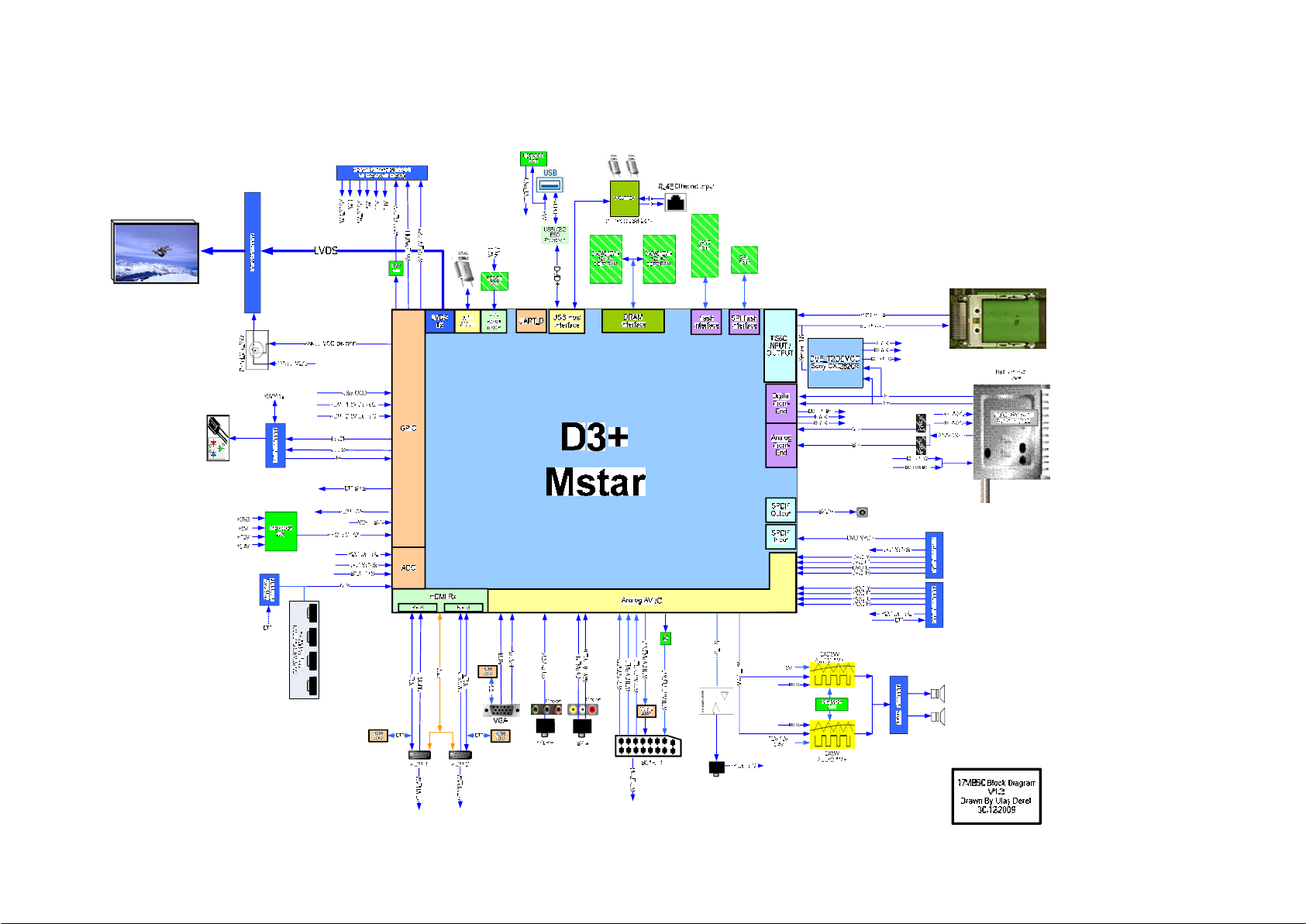
1.1. General Block Diagram
Page 7
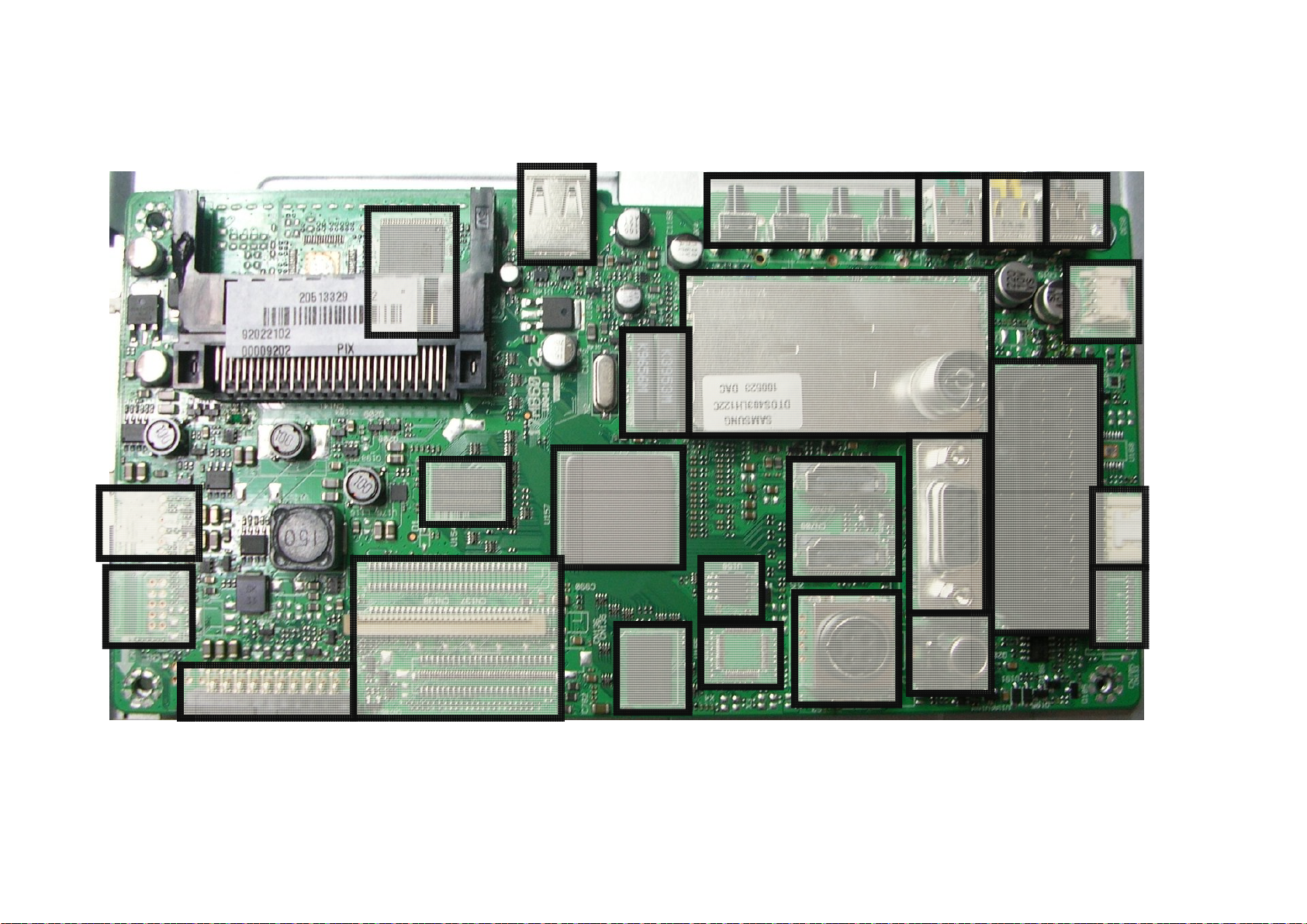
1.2. MB60 Placement of Blocks
(
)
External
Keyboard
Touchboard
DVD
Connector
CI Connector
Power Connector
Nand
Flash
(U162)
Connectors
DDR2
RAM
(U154)
LVDS
USB
Saw
Filters
Main IC
(U157)
DDR2
RAM
(U155)
SPI
Flash
Ethernet
IC
U171
Keypad
Tuner(TU102)
HDMI
Connectors
Ethernet
Connector or
Adapter DC
Input
YPbPr SAV HP
SCART
Connector
VGA
SPDIF
Out
Speaker
Con.
Led
Con
Inv.
Con
Page 8
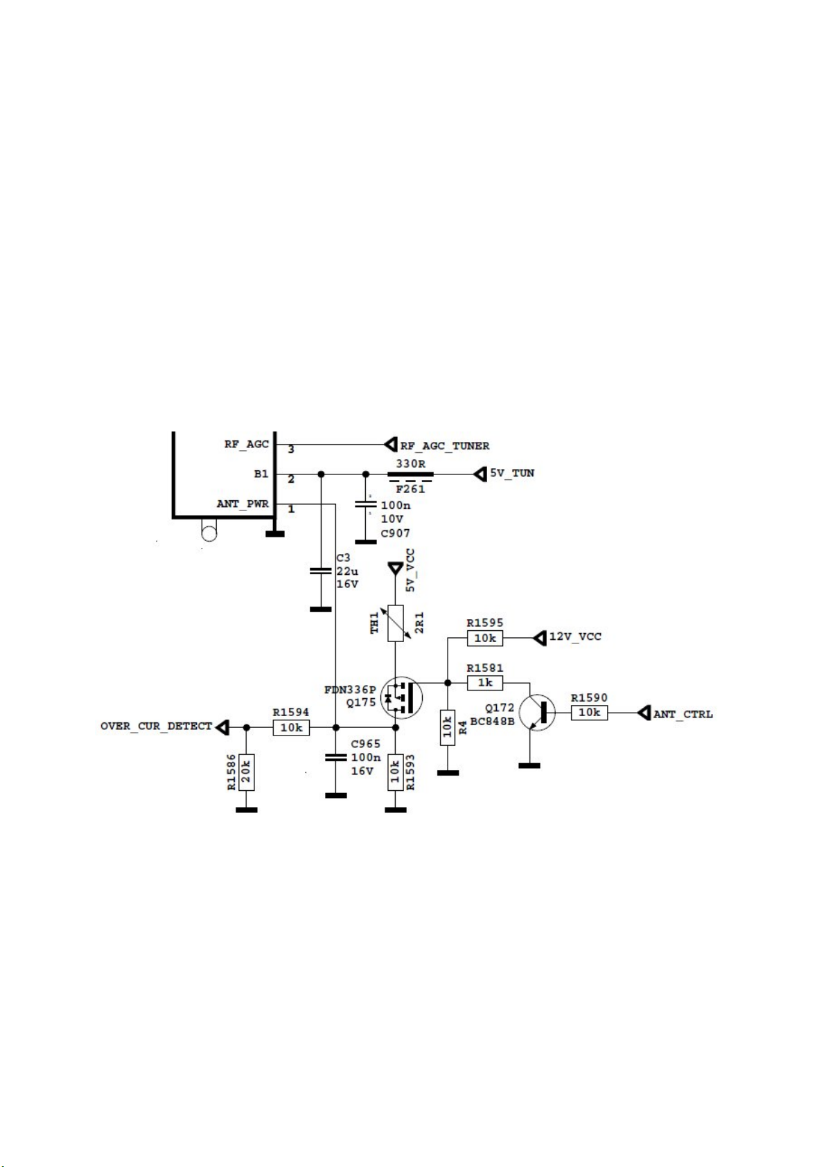
1. TUNER(TU102)
A horizontal mounted and Digital Half-Nim tuner is used in the product, which covers 3
Bands(From 48MHz to 862MHz for COFDM, from 45.25MHz to 863.25MHz for CCIR CH).
The tuning is available through the digitally controlled I2C bus (PLL). Below you will find
info about the tuner.
In active antenna option, the following circuit are used. ANT_CTRL pin is controlled by
microcontroller. If ANT_CTRL is low, ANT_PWR will be low. If ANT_CTRL is high,
ANT_PWR will be high.
OVER_CUR_DETECT pin is a monitor for short circuit in antenna. OVER_CUR_DETECT
is low, ANT_CTRL will be low, so ANT_PWR will be low. Finally, short circuit protection is
done by circuits and microcontroller.
1.1. General description of Samsung DTOS403LH122X:
The Tuner covers 3 Bands(from 48MHz to 862MHz for COFDM, from 45.25MHz to
863.25MHz for CCIR CH). Band selection and Tuning are performed digitally via the I2C
bus.
1.2. Features of DTOS403LH122X:
x Receiving System: This TUNER is designed to cover the air channels in VHF and
UHF, compliant with DVB-T standard. and It covers all Analog channels from
48.25MHz to 863.25MHz
Page 9

x Receiving Channel (Digital, Center frequency):
VHF Low CH. E2 ~ S10 ( 50.5MHz ~ 170.5MHz )
VHF High CH. E5 ~ S41 ( 177.5MHz ~ 466 MHz )
UHF CH. E21 ~ E69 ( 474 MHz ~ 858 MHz )
x Receiving Channel (PAL, Picture carrier frequency):
VHF Low CH. E2 ~ S10 ( 48.25MHz ~ 168.25MHz )
VHF High CH. E5 ~ S41 ( 175.25MHz ~ 463.25MHz )
UHF CH. E21 ~ E70 ( 471.25MHz ~ 863.25MHz )
x Intermediate Frequency:
Digital(center) DVB-T (36.167 MHz)
Digital(center) DVB-C (36.125 MHz)
Analog(picture) 38.9 MHz
x Input Impedance: 758QEDODQFHG
x Band Change-Over System
PLL Control System
x Tuning System
Electronic Tuning System With PLL
x Internal(or External) RF AGC function
Built in wideband AGC detector with 6 programmable take-over points
1.3. Pinning:
Terminal
Pin no.
10 IF OUT + Output 2 of the IF Amplifier
11 IF OUT - Output 1 of the IF Amplifier
12 AIF Output IF output of the Analog BroadBand
Name Pin Description
1 Ant Power Active Antenna Power
2 B+ +5V, Supply Voltage (Preamplifier, DC/DC)
3 RF AGC RF AGC (internal or external mode)
4 CL I2C Serial Clock
5 DA I2C Serial Clock
6 BP +5V, Supply Voltage (RF Amp, PLL, IF Amp)
7 BT(T.P) +33V, within DC/DC circuit
8 AS I2C Address Selection of the PLL
9 IF AGC Control voltage for the IF AGC
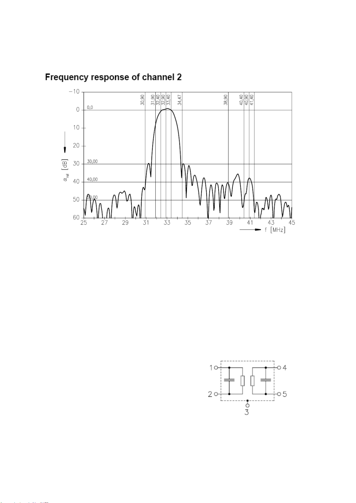
2. SAW FILTER – Audio – Epcos K9656M(Z101)
2.1. Standart
x B/G
x D/K
x I
x L/L’
Page 10
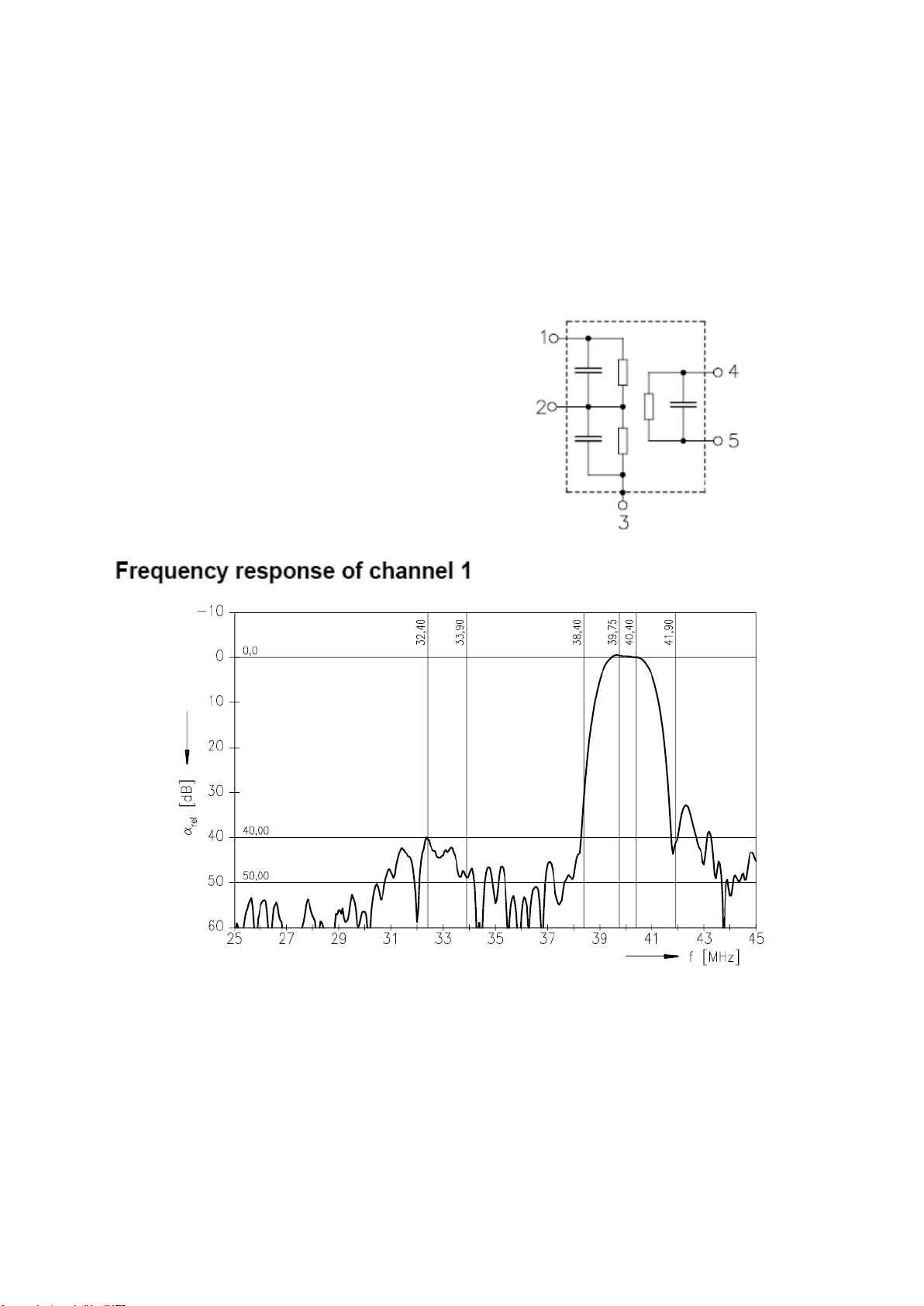
2.2. Features
x TV IF audio filter with two channels
x Channel 1 (L’) with one pass band for sound carriers at 40,40 MHz (L’) and 39,75
MHz (L’- NICAM)
x Channel 2 (B/G,D/K,L,I) with one pass band for sound carriers between 32,35 MHz
and 33,40 MHz
2.3. Pin configuration
1 Input
2 Switching input
3 Chip carrier - ground
4 Output
5 Output
2.4. Frequency response
Page 11
3. SAW FILTER – Video – Epcos K3958M(Z102)
3.1. Standart
x B/G
x D/K
x I
x L/L’
3.2. Features
x TV IF filter with Nyquist slopes at 33.90 MHz and 38.90 MHz
x Constant group delay
Pin configuration:
1 Input
2 Input - ground
3 Chip - carrier ground
4 Output
5 Output
Page 12
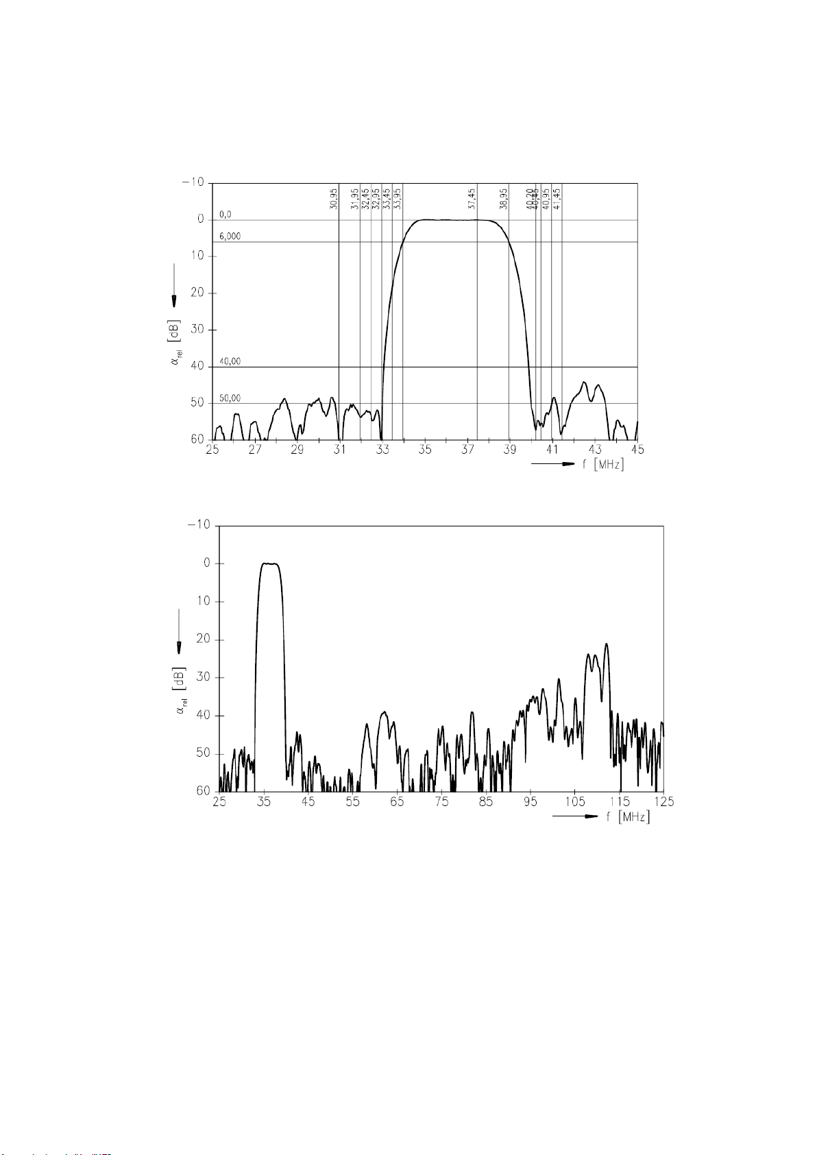
3.3. Frequency response
4. AUDIO AMPLIFIER STAGE WITH AZAD2102(U163, U164)
4.1. General Description
17MB60 uses two 2,5W Class D Mono Audio Amplifers for from 16” to 24” TVs.
$=$'% LV D :DWWV PD[ FDQ RIIHU :DWWV # /RDG ȍ7+'
AVdd=DVdd=5.5Volt)with high efficiency filter-free class-D audio power amplifier in a
1613 mm x 1613 mm wafer chip scale package (WCSP). AZAD2102B uses Currentswitch technology to achieve high performance class-d amplifier that features 0.03%
THD, 85% efficiency, –70 dB PSRR, to improve RF-rectification immunity.
Page 13

AZAD2102B provide a Vibration-Spectrum modulation clock for PWM Output. This
vibration frequency is around 10KHZ shift (+/- 5KHZ of Fpwm).
The advantage of the small size package (WCSP) makes AZAD2102B very suitable for
mobile phone and PDA device application. And the Class-D amplifier structure let
AZAD2102B to have highly efficiency power consumption than Class-AB amplifier.
AZAD2102B can shrink the application board, reduce system cost, and external
components.
ESD level protection I/O embedded in AZAD2102B. For general applications, doesn’t
need to add extra ESD protection device (like Varistors) in application system for
AZAD2102B’s I/O.
4.2. Features
x CMOS Technology
x High Efficiency 85%
x High PSRR 70dB at 217Hz
x Differential OP-amp Input
x AZAD2102B provides Vibration-Spectrum Modulation clock for reduce EMI
x Provide Mute function(set Mute_B to GND will go into Mute status)
x For the input stage AZAD2102B built-in a 10Kohm resistors (Gain setting=29.5dB)
x Maximum Battery Life and Minimum Heat
x Efficiency With an 8-ȍ6SHDNHU
x 3.5 mA Quiescent Current
x Output Power at 10% THD
x :DWWVDW$9GG '9GG 9ROW5ORDG ȍ
x 1.45WatWVDW$9GG '9GG 9ROW5ORDG ȍ
x :DWWVDW$9GG '9GG 9ROW5ORDG ȍ
x :DWWVDW$9GG '9GG 9ROW5ORDG ȍ
x :DWWVDW$9GG '9GG 9ROW5ORDG ȍ
x :DWWVDW$9GG '9GG 9ROW5ORDG ȍ
x Eliminate Power on and Power-off “Pop” noise
x A Fewer External Components
x Optimized PWM Output Stage Eliminates LC Output Filter
x Internally generate 290 kHz Switching Frequency to eliminate Capacitor and
Resistor
x Improve PSRR (–70 dB) and Wide Supply Voltage (3.0 V to 5.5 V)
x Fully Differential Design Reduces RF Rectification
x This chip has been built-in a very strong ESD protection.
x System level ESD 4KV (IEC 61000-4-2 ESD Contact Level)
x Wafer Chip Scale Package (WCSP)
x TSSOP Package with Exposed Pad
Page 14
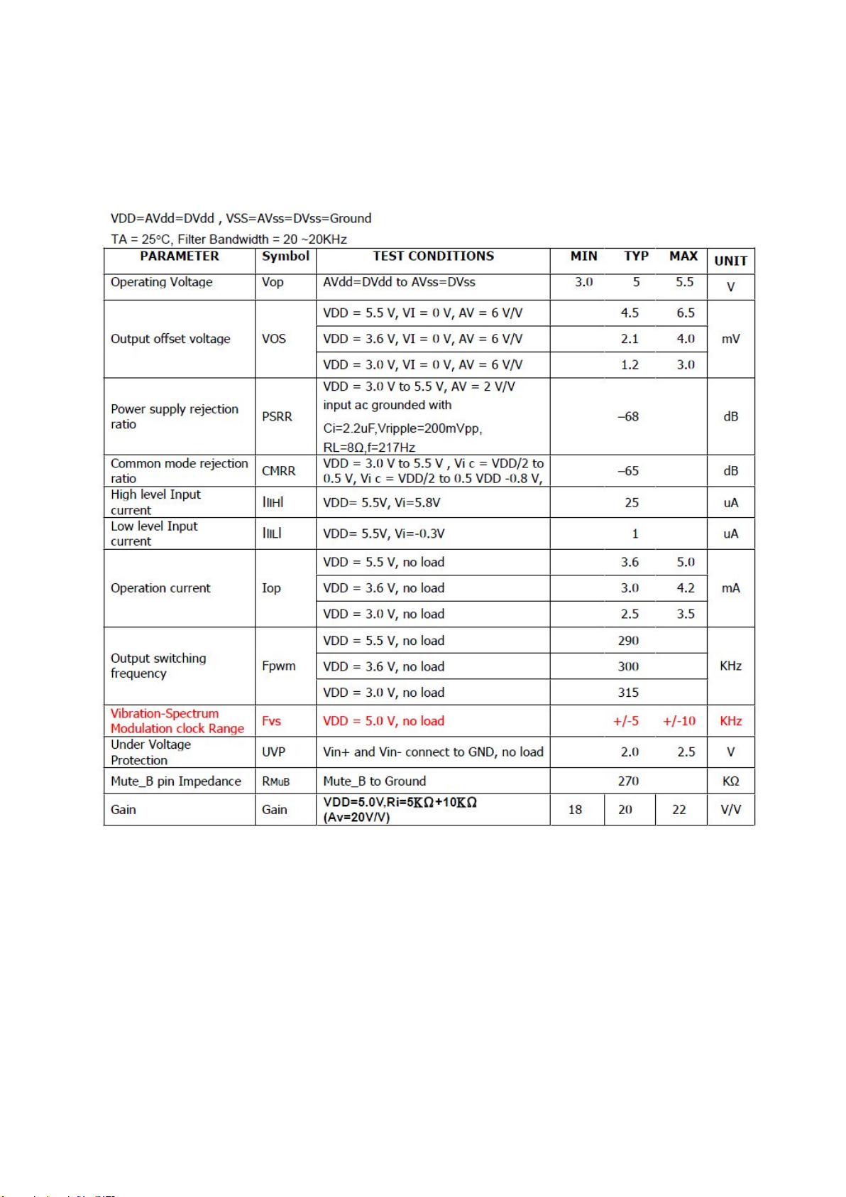
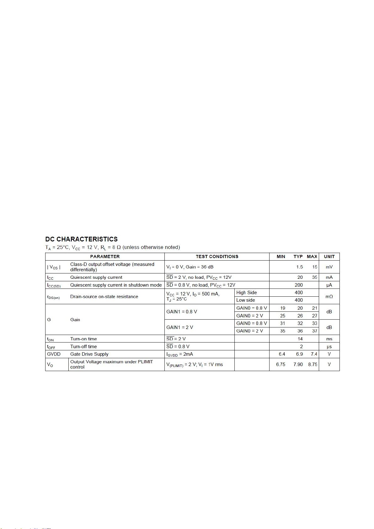
4.3. Absolute Ratings
4.3.1. Electrical Characteristics
Page 15
4.3.2. Operating Specifications
Page 16
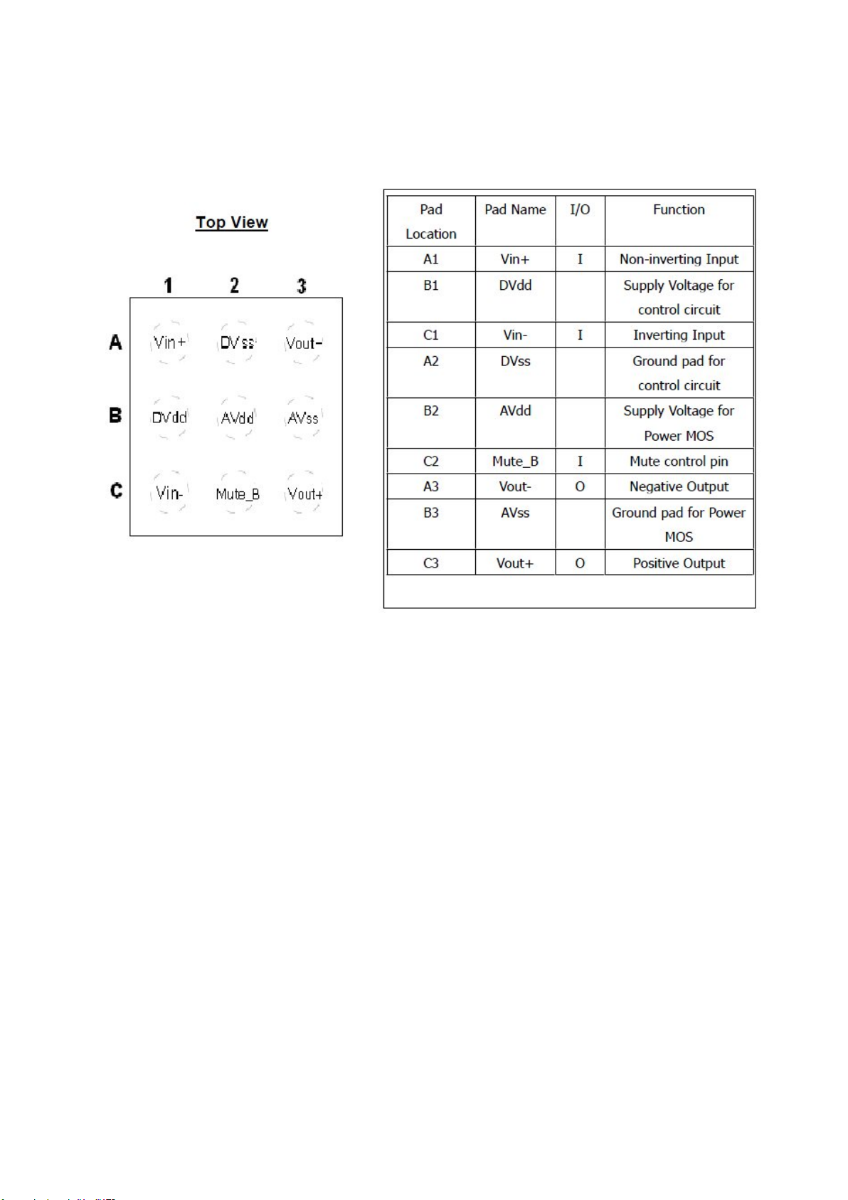
4.4. Pinning
5. AUDIO AMPLIFIER STAGE WITH TPA3113(U168)
5.1. General Description
17MB60 uses a 6W Class D Mono Audio Amplifers for from 26” to 32” TVs. The
TPA3113D2 is a 6-W (per channel) efficient, Class-D audio power amplifier for driving
bridged-tied stereo speakers. Advanced EMI Suppression Technology enables the use of
inexpensive ferrite bead filters at the outputs while meeting EMC requirements.
SpeakerGuard™ speaker protection circuitry includes an adjustable power limiter and a
DC detection circuit. The adjustable power limiter allows the user to set a "virtual" voltage
rail lower than the chip supply to limit the amount of current through the speaker. The DC
detect circuit measures the frequency and amplitude of the PWM signal and shuts off the
output stage if the input capacitors are damaged or shorts exist on the inputs.
The TPA3113D2 can drive stereo speakers as low as 4
TPA3113D2, 87%, eliminates the need for an external heat sink when
playing music.
The outputs are also fully protected against shorts to GND, VCC, and output-to-output.
The short-circuit protection and thermal protection includes an auto-recovery feature.
ȍ. The high efficiency of the
Page 17
5.2. Features
x 6-W/ch into an 8-ȍ Loads at 10% THD+N From a 10-V Supply
x 12-W into a 4-ȍ Mono Load at 10% THD+N From a 10-V Supply
x 87% Efficient Class-D Operation Eliminates Need for Heat Sinks
x Wide Supply Voltage Range Allows Operation from 8 V to 26 V
x Filter-Free Operation
x SpeakerGuard™ Speaker Protection Includes Adjustable Power Limiter plus DC
Protection
x Flow Through Pin Out Facilitates Easy Board Layout
x Robust Pin-to-Pin Short Circuit Protection and Thermal Protection with Auto
Recovery Option
x Excellent THD+N / Pop-Free Performance
x Four Selectable, Fixed Gain Settings
x Differential inputs
5.3. Absolute Ratings
5.3.1. Electrical Characteristics
Page 18
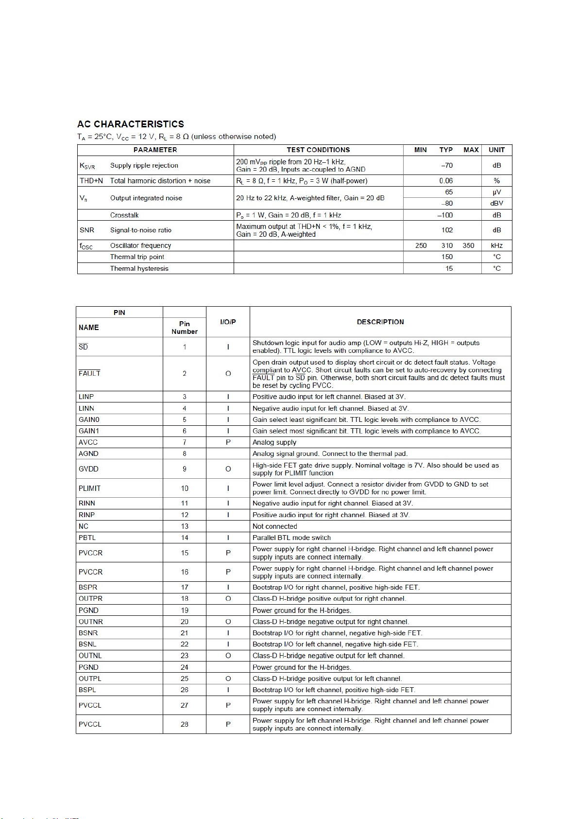
5.3.2. Operating Specifications
5.4. Pinning
Page 19
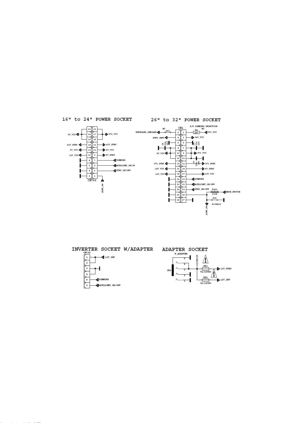
6. POWER STAGE
The DC voltages required at various parts of the chassis and panel are provided by a
main power supply unit. MB60 chassis can operate with IPS60, IPS16, IPS17, PW26,
PW27 as main power supply and also with 12V adaptor.
CN706 is used for IPS60, IPS16 and IPS17 and CN1 is used for PW26 and PW27.
JK9 is used for the adapter option and also CN705 inverter socket or DB32 chassis with
CN706 is used to supply backlight.
The power supplies generate 18V, 12V, 5V, 3,3V and 12V, 5V, stand by mode DC
voltages. Power stage which is on-chassis generates 5V, 3V3 stand by voltage and 12V,
8V, 5V, 3V3, 2.5V, 1,8V and 1,2V supplies for other different parts of the chassis. Chassis
block diagram is indicated below.
Page 20
The blocks on power block diagram is using dependent to main supply. For PW26 and
PW27 just common blocks are enough for proper operation.
For IPS16, IPS17, IPS60 below blocks must work properly.
For adopter case also below blocks are necessary.
Page 21
Short CCT Protection Circuit
Short circuit protection is necessary for protecting chassis and main IC against damages
when any Vcc supply shorts to ground. Protect pin should be logic high while normal
operation. When there is a short circuit protect pin shold be logic low. After any short
detection, SW forces LEDs on LED card to blink.
Page 22
6.1. Power Management
Page 23
7. MICROCONTROLLER – MSTAR(U157)
7.1. General Descripction
The MSD9WB7PX-2 integrates DTV/multi-media all-purpose AV decoder, DVB-T
demodulator, VIF demodulator, and Sound/Video processor into a single device. This
allows the overall BOM to be reduced significantly making the MSD9WB7PX-2 a very
Page 24

competitive multi-media DTV solution. For ATV users, the MSD9WB7PX-2 provides multistandard analog TV support with adaptive 3D video decoding and VBI data extraction.
The build-in audio decoder is capable of decoding FM, AM, NICAM, A2, BTSC and EIA-J
sound standards. The MSD9WB7PX-2 supplies all the necessary A/V inputs and outputs
to complete a receiver design including a multi-port HDMI receiver and component video
ADC. All input selection multiplexed for video and audio are integrated, including full
SCART support with CVBS output. The equipped MStar MACE-5 color engine is the
latest masterpiece from MStar famous color engine series providing excellent video and
picture quality in Full-HD and large-scale displaying system. To meet the increasingly
popular energy legislative requirements without the use of additional hardware, the
MSD9WB7PX-2 has an ultra low power standby mode during which an embedded MCU
can act upon standby events and wake up the system as required.
7.2. General Features
MSD9WB9PX-2, an SOC solution that supports channel decoding, MPEG decoding, and
media-centre functionality enabled by a high performance AV CODEC and CPU Key
features include,
x Digital and Analog DVB Front-End Demodulator
x A Multi-Standard A/V Format Decoder
x The MACE-5 Video Processor
x Home Theater Sound Processor
x Peripheral and Power Management
Transport Stream De-multiplexer
x Supports parallel and serial TS interface, with or without sync signal
x Supports TS input and output for external CI module
x Maximum TS data rate is 104 Mb/sec for serial or 16 MB/sec for parallel
x 32 general purpose PID filters and section filters for each transport stream de-
multiplexer
x Supports additional audio/video/PCR filters
x Supports TS DMA channel for time-shift
x Supports 3DES/DES and AES encryption/decryption
MPEG-2 Video Decoder
x ISO/IEC 13818-2 MPEG-2 video MP@HL
x Automatic frame rate conversion
x Supports resolution up to HDTV (1080i, 720p) and SDTV
MPEG-4 Video Decoder
x ISO/IEC 14496-2 MPEG-4 ASP video decoding
x Supports resolutions up to HDTV (1080p@30fps)
x Supports DivX1 Home Theater & HD profilesOptional
x Supports VC-1Optional, FLV video format decoding
H.264 Decoder
x ITU-T H.264, ISO/IEC 14496-10 (main and high profile up to level 4.1) video
decoding
Page 25

x Supports resolutions for all DVB, ATSC, HDTV, DVD and VCD
x Supports resolution up to 1080p@30fps
x Supports CABAC and CAVLC stream types
x Processing of ES and PES streams, extraction and provision of time stamps
x Up to 40 Mbits bitrate (Blu-ray spec.)
Hardware JPEG
x Supports sequential mode, single scan
x Supports both color and grayscale pictures
x Following the file header scan the hardware decoder fully handles the decode
process
x Supports programmable Region of Interest (ROI)
x Supports formats: 422/411/420/444/422T
x Supports scaling down ratios: 1/2, 1/4, 1/8
x Supports picture rotation
NTSC/PAL/SECAM Video Decoder
x Supports NTSC-M, NTSC-J, NTSC-4.43, PAL (B, D, G, H, M, N, I, Nc), and
SECAM standards
x Automatic standard detection
x Motion adaptive 3D comb filter
x Five configurable CVBS & Y/C S-video inputs
x Supports Teletext, Closed Caption (analog CC 608/ analog CC 708/digital CC
608/digital CC 708), V-chip and SCTE
Multi-Standard TV Sound Processor
x SIF audio decoding
x Supports BTSC/A2/EIA-J demodulation
x Supports NICAM/FM/AM demodulation
x Supports MTS Mode Mono/Stereo/SAP in BTSC/EIA-J mode
x Supports Mono/Stereo/Dual in A2/NICAM mode
x Built-in audio sampling rate conversion (SRC)
x Audio processing for loudspeaker channel, including volume, balance, mute, tone,
EQ, virtual stereo/surround and treble/bass controls
x Advanced sound processing options available, for example: Dolby, SRS, BBE,
QSound, Audyssey
x Supports digital audio format decoding:
x MPEG-1, MPEG-2 (Layer I/II), MP3, Dolby Digital (AC-3), AAC-LC
x Supports Optional Dolby Digital Plus, Dolby Pulse, and MS10 multistream
decoder, including Dolby Digital Encoder for transcoding streams to Dolby Digital
5.1 (DDCO)
x Supports MPEG Audio, Dolby Digital, Dolby Digital Plus format AD (Audio
Description)
x Supports PVR and time-shifting
Audio Interface
One SIF audio input interface with minimal external saw filters
Page 26

x Four L/R audio line-inputs including Mic. input
x Two L/R outputs for main speakers and additional line-outputs
x Supports stereo headphone driver
x I2S digital audio input & output
x S/PDIF digital audio output
x HDMI audio channel processing
x Programmable delay for audio/video synchronization
Analog RGB Compliant Input Port
x Three analog ports support up to 1080P
x Supports PC RGB input up to SXGA@75Hz
x Supports HDTV RGB/YPbPr/YCbCr
x Supports Composite Sync and SOG Sync-on-Green
x Automatic color calibration
x AV-link support
Analogue RGB Auto-Configuration & Detection
x Auto input signal format and mode detection
x Auto-tuning function including phasing, positioning, offset, gain, and jitter detection
x Sync Detection for H/V Sync
DVI/HDCP/HDMI Compliant Input Port
x Three HDMI/DVI Input ports
x HDMI 1.3 Compliant
x HDCP 1.1 Compliant
x 225MHz @ 1080P 60Hz input with 12-bit Deep-color support
x CEC support
x Single link DVI 1.0 compliant
x Robust receiver with excellent long-cable support
MStar Advanced Color Engine (MStarACE-5)
x 10/12-bit internal data processing
x Fully programmable multi-function scaling engine
x Nonlinear video scaling supports various modes including Panorama
x Supports dynamic scaling for VC-1
x High-Quality DTV video processor
x 3D motion video deinterlacer with motion object stabilizer
x Edge-oriented deinterlacer with edge and artifact smoother
x Automatic 3:2/2:2/M:N pull-down detection and recovery
x 3D multi-purpose noise reduction for DTV or lousy air/cable input
x MPEG artifact removal including de-blocking and mosquito noise reduction
x Arbitrary frame rate conversion
x MStar Professional Picture Enhancement:
o Dynamic brilliant and fresh color
o Dynamic Blue Stretch
o Intensified contrast and details
o Dynamic Vivid Skin
Page 27

o Dynamic sharpened Luma/Chroma edges
o Global and local dynamic depth of field perception
o Accurate and independent color control
o Supports sRGB and xvYCC color processing
o Supports HDMI 1.3 deep color format
x Programmable 12-bit RGB gamma CLUT
Output Interface
x Single/dual link 8/10-bit LVDS output
x Supports panel resolution up to Full-HD (1920x1080) @ 60Hz
x Supports TH/TI format
x Supports dithering options to 6/8-bit output
x Spread spectrum output for EMI suppression
CVBS Video Encoder
x Supports all NTSC/PAL TV Standard
x Stand-alone scaling engine
x Programmable Hue, Contract, Brightness
x Supports TTX/CC/WSS output
CVBS Video Output
x Allows CVBS output of all source inputs
2D Graphics Engine
x Hardware Graphics Engine for responsive interactive applications
x Supports point draw, line draw, rectangle draw/fill, text draw and trapezoid draw
x BitBlt, stretch BitBlt, trapezoid BitBlt, mirror BitBlt and rotate BitBlt
x Raster Operation (ROP)
x Support Porter-Duff
VIF Demodulator
x Compliant with NTSC M/N, PAL B, G/H, I, D/K, SECAM L/L' standards
x Audio/Video dual-path processor
x Stepped-gain PGA with 25 dB tuning range and 1 dB tuning resolution
x Maximum IF gain of 37 dB
x Programmable TOP to accommodate different tuner gain and SAW filter insertion
loss to optimize noise and linearity performance
x Multi-standard processing with single SAW
x Supports silicon tuner low IF output architecture
DVB-T/DVB-C Demodulator
x Digital carrier frequency offset correction: ±500KHz
x Optimised for SFN channels with pre/post-cursive echoes inside/outside the guard
x Acquisition range ±857kHz includes up to 3x: ±1/6 MHz transmitter offset
x Meets Nordig Unified 1.0.3, D-Book 5.0, EICTA E-Book/C-Book test requirement
x ITU J.83 Annex A/C, DVB-C (EN 300 429) compliant
x Supports DVB-C 0.7-7M Baud symbol rate
Page 28

x ±400kHz internal carrier offset recovery range
x 6.8 usecs echo cancellation at 7 Msym/s
x Supports IF, low-IF, zero-IF inputs
x Ultra-fast automatic blind UHF/VHF channel scan (constellations and symbol rate)
Connectivity
x Two USB 2.0 host ports
x USB architecture designed for efficient suppor of external storage devices in
conjunction with off air broadcasting
Miscellaneous
x DRAM interface supporting two 16-bit DDR2 @ 1066MHz
x Supports PVR
x Supports Common Interface for conditional access support
x Bootable SPI interface with serial flash support
x Parallel interface for external OneNAND and NAND flash support
x Power control module with ultra low power
x MCU available in standby mode
x 523-ball LFBGA package
x Operating Voltages: 1.26V (core), 1.8V (DDR2), 2.5V and 3.3V (I/O and analog)
7.3. MSTAR Block Diagram
Page 29

7.4. Reset Circuit
Reset circuit using for initiliazing main Mstar IC. Reset condition is high and nomal
working condition is low for RESET pin.
8. CI INTERFACE
7.1 Block Diagram
Page 30

7.1 CI Interface Power Switch
It is used for CI module supply, when Module is inserted (it means CI detect is low) This
circuit is opened or closed by CI_POWER_CTRL port of main uController
9. T2 Demodulator CXD2820R (U167)
9.1. General Description
This demodulator is optionall for support T2 reception. The Sony CXD2820R is a
combined DVB-T2, DVB-T and DVB-C demodulator that conforms to the ETSI EN 302755 (second generation Terrestrial) ETSI EN 300-744 (Terrestrial) and ETSI EN 300-429
(Cable) standards.
9.2. Features
x Single, 41MHz crystal (can be shared with CXD2813Ranalogue demod IC)
x High performance differential signal ADC
x RF power level monitor ADC
x Low IF and high IF (36MHz) mode input
x Fast 400kHz I2C compatible bus interface
Page 31

x Quiet I2C interface for dedicated tuner control
x Automatic IF AGC and optional programmable
x RF AGC/GPIO functions
x Configurable parallel and serial MPEG-2 TS outputs with smoothing buffer
x 3.3V, 2.5V, 1.2V supplies
x Temperature range -20°C to +85°C
x Supplied with full reference design, including software driver, PCB
schematic/layouts, GUI and documentation
x 3.3V for VDD and 2.5V for VDDQ power supply
x All inputs and outputs are compatible with SSTL_2 interface
x JEDEC standard 400mil 66pin TSOP-II with 0.65mm pin pitch
x Fully differential clock inputs (CK, /CK) operation
x Double data rate interface
x Source synchronous - data transaction aligned to bidirectional data strobe (DQS)
x x16 device has 2 bytewide data strobes (LDQS, UDQS) per each x8 I/O
x Data outputs on DQS edges when read (edged DQ) Data inputs on DQS centers
when write (centered DQ)
x Data(DQ) and Write masks(DM) latched on the both rising and falling edges of the
data strobe
x All addresses and control inputs except Data, Data strobes and Data masks
latched on the rising edges of the clock
x Write mask byte controls by LDM and UDM
x Programmable /CAS latency 3 / 4 supported
x Programmable Burst Length 2 / 4 / 8 with both sequential and interleave mode
x Internal 4 bank operations with single pulsed /RAS
x tRAS Lock-Out function supported
x Auto refresh and self refresh supported
x 4096 refresh cycles / 32ms
x Full, Half and Matched Impedance(Weak) strength driver option controlled by
EMRS
Page 32

9.3. Pinning
Page 33

Page 34

Page 35

10. USB INTERFACE
Main Concept IC has integrated 2 USB 2.0 interface. One of them is used for ethernet
function, the other one is used for USB connectivity for last user. Last user can play video,
picture and audio files. Also digital channels can be record to externall storage device by
this interface. All SW files can be updated with interface.
USB circuit has 3 main parts
x Integrated USB 2.0 Host interface of D3 (U157)
x Protection IC (U145)
x Over Curent Protection IC (U149)
11. DDR2 SDRAM 8M × 4 BANKS × 16 BIT (W9751G6JB)
(U154, U155)
11.1. General Description
The W9751G6JB is a 512M bits DDR2 SDRAM, organized as 8,388,608 words × 4 banks
× 16 bits. This device achieves high speed transfer rates up to 1066Mb/sec/pin (DDR2-
1066) for general applications. W9751G6JB is sorted into the following speed grades: -18,
-25 and -3. The -18 is compliant to the DDR2-1066/CL7 specification. The -25 is
compliant to the DDR2-800 (5-5-5) or DDR2-800 (6-6-6) specification. The -3 is compliant
to the DDR2-667 (5-5-5) specification. All of the control and address inputs are
synchronized with a pair of externally supplied differential clocks. Inputs are latched at the
cross point of differential clocks (CLK rising and CLK falling). All I/Os are synchronized
with a single ended DQS or differential DQS- DQS pair in a source synchronous fashion.
Page 36

11.2. Features
x Power Supply: VDD, VDDQ = 1.8 V± 0.1 V
x Double Data Rate architecture: two data transfers per clock cycle
x CAS Latency: 3, 4, 5, 6 and 7
x Burst Length: 4 and 8
x Bi-directional, differential data strobes (DQS andDQS ) are transmitted / received
with data
x Edge-aligned with Read data and center-aligned with Write data
x DLL aligns DQ and DQS transitions with clock
x Differential clock inputs (CLK and CLK )
x Data masks (DM) for write data
x Commands entered on each positive CLK edge, data and data mask are
referenced to both edges of DQS
x Posted CAS programmable additive latency supported to make command and data
bus efficiency
x Read Latency = Additive Latency plus CAS Latency (RL = AL + CL)
x Off-Chip-Driver impedance adjustment (OCD) and On-Die-Termination (ODT) for
better signal quality
x Auto-precharge operation for read and write bursts
x Auto Refresh and Self Refresh modes
x Precharged Power Down and Active Power Down
x Write Data Mask
x Write Latency = Read Latency - 1 (WL = RL - 1)
x Interface: SSTL_18
11.3. Electrical Characteristics
Page 37

11.4. Pinning
Page 38

Page 39

12. SCALER AND LVDS SOCKETS
12.1. LVDS sockets Block Diagram
12.2. Panel Supply Switch Circuit
This switch is used to open and close panel supply of TCON. It is controlled by port of
main ucontroller. Also with this circit panel sequency could be adjusted correctly. 3 panel
supplys are connected to this circuit. All of them are optional according to panels.
Page 40

13. NAND FLASH MEMORY - MX25L1005 (U158)
13.1. General Description
MX25L1005 is a CMOS 1,048,576 bit serial Flash memory, which is configured as
131,072 x 8 internally.The MX25L1005 feature a serial peripheral interface and software
protocol allowing operation on a simple 3-wire bus. The three bus signals are a clock
input (SCLK), a serial data input (SI), and a serial data output (SO). SPI access to the
device is enabled by CS# input. The MX25L1005 provide sequential read operation on
whole chip. After program/erase command is issued, auto program/ erase algorithms
which program/ erase and verify the specified page or sector/block locations will be
executed. Program command is executed on page (256 bytes) basis, and erase
command is executes on chip or sector(4K-bytes) or block(64K-bytes). To provide user
with ease of interface, a status register is included to indicate the status of the chip. The
status read command can be issued to detect completion status of a program or erase
operation via WIP bit. When the device is not in operation and CS# is high, it is put in
standby mode and draws less than 10uA DC current. The MX25L1005 utilize MXIC's
proprietary memory cell, which reliably stores memory contents even after 100,000
program and erase cycles.
13.2. Features
x Serial Peripheral Interface (SPI) compatible -- Mode 0 and Mode 3
x 1,048,576 x 1 bit structure
x 32 Equal Sectors with 4K byte each, Any Sector can be erased individually
x 2 Equal Blocks with 64K byte each, Any Block can be erased individually
x Single Power Supply Operation
Page 41

x 2.7 to 3.6 volt for read, erase, and program operations
x Latch-up protected to 100mA from -1V to Vcc +1V
x Low Vcc write inhibit is from 1.5V to 2.5V
13.3. Absolute Maximum Ratings
RATING VALUE
Ambient Operating
Temperature
Storage Temperature -55°C to 125°C
Applied Input Voltage -0.5v to 4.6v
Applied Output Voltage -0.5v to 4.6v
VCC to Ground Potential -0.5v to 4.6v
0°C to 70°C
13.4. Pinning
8-PIN SOP (150mil)
SYMBOL DESCRIPTION
CS# Chip select
SI Serial Data Input
SO Serial Data Output
SCLK Clock Input
HOLD# Hold, to pause the device without
deselecting the device
VCC +3.3v Power Supply
GND Ground
Page 42

14. NAND FLASH MEMORY – NAND512XXA2C (U162)
14.1. General Description
The NAND flash 528-byte/ 264-word page is a family of non-volatile flash memories that
uses the single level cell (SLC) NAND technology. It is referred to as the small page
family.
The NAND512R3A2C, NAND512R4A2C, and NAND512W3A2C have a density of 512
Mbits and operate with either a 1.8 V or 3 V voltage supply. The size of a page is either
528 bytes (512 + 16 spare) or 264 words (256 + 8 spare) depending on whether the
device has a x8 or x16 bus width.
The address lines are multiplexed with the Data Input/Output signals on a multiplexed x8
or x16 input/output bus. This interface reduces the pin count and makes it possible to
migrate to other densities without changing the footprint.
To extend the lifetime of NAND flash devices it is strongly recommended to implement an
error correction code (ECC). The use of ECC correction allows to achieve up to 100,000
program/erase cycles for each block. A write protect pin is available to give a hardware
protection against program and erase operations.
14.2. Features
x High density NAND flash memories
o 512-Mbit memory array
o Cost effective solutions for mass storage applications
x NAND interface
o x8 or x16 bus width
o Multiplexed address/ data
x Supply voltage: 1.8 V, 3 V
x Page size
o x8 device: (512 + 16 spare) bytes
o x16 device: (256 + 8 spare) words
x Block size
o x8 device: (16K + 512 spare) bytes
o x16 device: (8K + 256 spare) words
x Page read/program
o Random access: ȝV9ȝV9PD[
o Sequential access: 30 ns (3 V)/50 ns (1.8 V) (min)
o 3DJHSURJUDPWLPHȝVW\S
x Copy back program mode
x Fast block erase: 2 ms (typ)
Page 43

x Status register
x Electronic signature
x Chip Enable ‘don’t care’
x Security features
o OTP area
x Serial number (unique ID) option
x Hardware data protection
o Program/erase locked during power transitions
x Data integrity
o 100,000 program/erase cycles (with ECC)
o 10 years data retention
x RoHS compliant packages
x Development tools
o Error correction code models
o Bad blocks management and wear leveling algorithms
14.3. Pinning
Page 44

15. USB2.0 to Fast Ethernet – ASIX AX88X72A (U171)
15.1. General Description
The AX88772A/AX88172A Low-pin-count USB 2.0 to 10/100M Fast Ethernet controller is
a high performance and highly integrated ASIC which enables low cost, small form factor,
and simple plug-and-play Fast Ethernet network connection capability for desktops,
notebook PC’s, Ultra-Mobile PC’s, docking stations, game consoles, digital-home
appliances, and any embedded system using a standard USB port.
The AX88772A/AX88172A features a USB interface to communicate with a USB Host
Controller and is compliant with USB specification V1.1 and V2.0. The
AX88772A/AX88172A implements 10/100Mbps Ethernet LAN function based on
IEEE802.3, and IEEE802.3u standards with 24KB of embedded SRAM for packet
buffering. The AX88772A/AX88172A integrates an on-chip 10/100Mbps Ethernet PHY to
simplify system design.
The AX88172A provides an optional External Media Interface (EMI) for external PHY or
external MAC for different application purposes. The EMI can be a media-independent
interface (MII) for implementing 100BASE-FX Ethernet or HomePNA functions. The EMI
can also be a Reverse-MII or Reverse Reduced-MII (Reverse-RMII) for glueless MAC-toMAC connections to any MCU with Ethernet MAC MII or RMII interface. In addition, the
EMI can be configured to Dual-PHY mode allowing AX88172A to act as an Ethernet PHY
or USB 2.0 PHY for external MAC device that needs Ethernet and USB interfaces in their
system applications. The optional serial interface such as I2C, SPI, and UART are
provided as a control channel from the USB Host Controller to communicate with the
external MCU chip.
15.2. Features
Single chip USB 2.0 to 10/100M Fast Ethernet controller – AX88772A
USB Device Interface
x Integrates on-chip USB 2.0 transceiver and SIE compliant to USB Spec 1.1 and
2.0
x Supports USB Full and High Speed modes with Bus-Power or Self-Power
capability
x Supports 4 or 6 programmable endpoints on USB interface
x High performance packet transfer rate over USB bus using proprietary burst
transfer mechanism
x Supports USB to Ethernet bridging or vice versa in hardware
Fast Ethernet Controller
x Integrates 10/100Mbps Fast Ethernet MAC/PHY
x IEEE 802.3 10BASE-T/100BASE-TX compatible
x Supports twisted pair crossover detection and auto-correction (HP Auto-MDIX)
x Embedded 16KB SRAM for RX packet buffering and 8KB SRAM for TX packet
buffering
x Supports both Full-duplex with flow control and
Page 45

x Half-duplex with backpressure operation
x Supports 2 VLAN ID filtering, received VLAN Tag (4 bytes) can be stripped off or
preserved MAC/PHY loop-back diagnostic capability
Support Wake-on-LAN Function
x Supports Suspend Mode and Remote Wakeup via Link-up, Magic packet, MS
wakeup frame and external pin
x Optional PHY power down during Suspend Mode
Versatile External Media Interface
x Optional MII interface in MAC mode allows AX88172A to work with external
100BASE-FX Ethernet PHY or HomePNA PHY
x Optional Reverse-MII or Reverse-RMII interface in PHY mode allows AX88172A to
work with external HomePlug PHY or glueless MAC-to-MAC connections
x Optional Reverse-MII interface in Dual-PHY mode allows AX88172A to act as an
Ethernet PHY or USB 2.0 PHY for external MAC device that needs Ethernet and
USB in system application
x Supports 256/512 bytes (93c56/93c66) of serial EEPROM (for storing USB
Descriptors)
x Supports automatic loading of Ethernet ID, USB Descriptors and Adapter
Configuration from EEPROM after power-on initialization
x Provides optional serial interface, I2C, SPI and UART
x Integrates on-chip voltage regulator and only requires a single 3.3V power supply
x 12MHz and 25Mhz clock input from either crystal or oscillator source
x Integrates on-chip power-on reset circuit
15.3. Block Diagram
Page 46

15.4. Pinning
16. LM1117(U175, U180, U181)
16.1. General Description
The LM1117 is a series of low dropout voltage regulators with a dropout of 1.2V at 800mA
of load current. It has the same pin-out as National Semiconductor’s industry standard
LM317. The LM1117 is available in an adjustable version, which can set the output
voltage from 1.25V to 13.8V with only two external resistors. In addition, it is also
available in five fixed voltages, 1.8V, 2.5V, 2.85V, 3.3V, and 5V. The LM1117 offers
current limiting and thermal shutdown. Its circuit includes a zener trimmed bandgap
reference to as-sure output voltage accuracy to within ±1%. The LM1117 series is
available in SOT- 223, TO-220, and TO-252 D-PAK packages. A mi
tantalum capacitor is required at the output to improve the transient response and
stability.
16.2. Features
x Available in 1.8V, 2.5V, 2.85V, 3.3V, 5V, and Adjustable Versions
x Space Saving SOT-223 Package
x Current Limiting and Thermal Protection
x Output Current 800mA
x Line Regulation 0.2% (Max)
x Load Regulation 0.4% (Max)
x Temperature Range
x LM1117 0°C to 125°C
x LM1117I -40°C to 125°C
QLPXP RI ȝ)
Page 47

16.3. Applications
x 2.85V Model for SCSI-2 Active Termination
x Post Regulator for Switching DC/DC Converter
x High Efficiency Linear Regulators 15
x 32” TFT TV Service Manual 10/01/2005
x Battery Charger
x Battery Powered Instrumentation
16.4. Absolute Maximum Ratings
16.5. Pinning
17. MP2012 (U176)
17.1. General Description
The MP2012 is a fully integrated, internally compensated 1.2MHz fixed frequency PWM
step-down converter. It is ideal for powering portable equipment that runs from a single
cell Lithium-Ion (Li+) Battery, with an input range from 2.7V to 6V. The MP2012 can
provide up to 1.5A of load current with output voltage as low as 0.8V. It can also operate
at 100% duty cycle for low dropout applications. With peak current mode control and
internal compensation, the MP2012 is stable with ceramic capacitors and small inductors.
Fault condition protection includes cycle-by-cycle current limiting and thermal shutdown.
17.2. Features
x 2.7-6V Input Operation Range
x Output Adjustable from 0.8V to VIN
x ȝ$0D[6KXWGRZQ&XUUHQW
x Up to 95% Efficiency
Page 48

x 100% Duty Cycle for Low Dropout
x Applications
x 1.2MHz Fixed Switching Frequency
x Stable with Low ESR Output Ceramic
x Capacitors
x Thermal Shutdown
x Cycle-by-Cycle Over Current Protection
x Short Circuit Protection
x Available in 6-pin 3x3mm QFN
17.3. Pinning
Pin
#
1 FB Feedback input. An external resistor divider from
2 GND,
3 SW Switch node to the inductor.
4 PVIN Input supply pin for power FET.
5 VIN Input Supply pin for controller. Put small
6 EN Enable input, “High” enables MP2012. EN is
Name Description
the output to GND, tapped to the FB pin sets the
output voltage.
Ground pin. Connect exposed pad to ground
Exposed
Pad
plane for proper thermal performance.
decoupling ceramic near this pin.
pulled to GND with 1Meg internal resistor.
18. RTA8283A (U23, U173)
18.1. General Description
The RT8283A is a high-efficiency, monolithic synchronous step-down DC/DC converter
that can deliver up to 3A output current from a 4.5V to 23V input supply. The RT8283A's
current mode architecture and external compensation allow the transient response to be
optimized over a wide range of loads and output capacitors. Cycle-by-cycle current limit
provides protection against shorted outputs and soft-start eliminates input current surge
during start-up. The RT8283A also provides output under voltage protection and thermal
VKXWGRZQSURWHFWLRQ7KHORZFXUUHQWȝ$VKXWGRZQPRGHSURYLGHVRXWSXWGLsconnect,
enabling easy power management in batterypowered systems. The RT8283A is available
in a SOP-8 package.
Page 49

18.2. Features
x ±1.5% High Accuracy Feedback Voltage
x Integrated N-MOSFET Switches
x Current Mode Control
x Fixed Frequency Operation : 340kHz
x Output Adjustable from 0.8V to 20V
x Up to 95% Efficiency
x Thermal Shutdown Protection
18.3. Pinning
Pin No. Pin
1 BOOT
2
3
4, 9 (Exposed
Pad)
5
6
7
8
Description
Name
Bootstrap for high-side gate driver. Connect a 0.1˩F or
greater ceramic capacitor from BOOT to SW pins.
VIN Input Supply 4.5V to 23V. Must bypass with a suitably
large ceramic capacitor.
SW Phase Node--Connect to external L-C filter..
GND Ground.
FB Feedback Input pin is connected to the converter output.
It is used to set the output of the converter to regulate to
the desired value via an internal res divider. For an
adjustable output, an external res divider is connected to
this pin.
COMP Compensation Node. COMP is used to compensate the
regulation Control loop. Connect a series RC network
from COMP to GND. In some cases, an additional
capacitor from COMP to GND is required.
EN Enable Input Pin. Logic high enables the converter; a
logic low forces the RT8253A into shutdown mode.
$WWDFKWKLVSLQWR9,1ZLWKDNȍ pull up resistor for
automatic startup.
SS Soft-Start Control Input. SS controls the soft-start period.
Connect a capacitor from SS to GND to set the soft-start
period. A 0.1˩F capacitor sets the soft-start period to
13.5ms.
19. MP1583 (U174)
19.1. General Description
The MP1583 is a step-down regulator with a built-in internal Power MOSFET. It achieves
3A of continuous output current over a wide input supply range with excellent load and
line regulation. Current mode operation provides fast transient response and eases loop
Page 50

stabilization. Fault condition protection includes cycle-by-cycle current limiting and thermal
shutdown. An adjustable soft-start reduces the stress on the input source at start-up. The
MP1583 requires a minimum number of external components, providing a compact
solution.
19.2. Features
x 3A Output Current
x Programmable Soft-Start
x Pȍ,QWHUQDO3RZHU026)(76ZLWFK
x Stable with Low ESR Output Ceramic Capacitors
x Up to 95% Efficiency
x ȝ$6KXWGRZQ0RGH
x Fixed 385KHz Frequency
x Thermal Shutdown
x Cycle-by-Cycle Over Current Protection
x Wide 4.75V to 23V Operating Input Range
x Output Adjustable from 1.22V to 21V
x Under-Voltage Lockout
19.3. Pinning
Pin
No.
1 BOOT High-Side Gate Drive Bootstrap Input. BS supplies the drive for the
2
3
4
5
6
7
8
Pin
Name
IN Power Input. Drive IN with a 4.75V to 23V power source.
SW Power Switching Out is the switching node that supplies power to the
GND Ground.
FB Feedback Input. FB senses the output voltage and regulates it. Drive
COMP Compensation Node is used to compensate the regulation control
EN Enable/UVLO. A voltage greater than 2.71V enables operation. For
SS Soft-Start Control Input. SS controls the soft-start period.
Description
high-side N-Channel MOSFET switch.
output
FB with a resistive voltage divider from the output voltage. FB
threshold is 1.222V.
loop.
complete low current shutdown the EN pin voltage needs to be at less
than 900mV. When the voltage on EN exceeds 1.2V, the internal
regulator will be enabled and the soft-start capacitor will begin to
charge. The MP1583 will start switching after the EN pin voltage
reaches 2.71V.
Page 51

20. FDC642
20.1. General Description
This P-Channel 2.5V specified MOSFET is produced using Fairchild’s advanced
PowerTrench® process that has been especially tailored to minimize on-state resistance
and yet maintain low gate charge for superior switching performance.
These devices have been designed to offer exceptional power dissipation in a very small
footprint for applications where the larger packages are impractical.
20.2. Features
x 0D[U'6RQ PȍDW9*6 -4.5 V, ID = -4.0 A
x 0D[U'6RQ PȍDW9*6 -2.5 V, ID = -3.2 A
x Fast switching speed
x Low gate charge (11nC typical)
x High performance trench technology for extremely low rDS(on)
x SuperSOTTM-6 package: small footprint (72% smaller than standard SO-8);
low profile (1 mm thick)
x Termination is Lead-free and RoHS Compliant
20.3. Pinning
21. FDC604P
21.1. General Description
This P-Channel 1.8V specified MOSFET uses Fairchild’s low voltage PowerTrench
process. It has been optimized for battery power management applications.
21.2. Features
x –5.5 A, –95'621 Pȍ#9*6 –4.5 V
x 5'621 Pȍ#9*6 –2.5 V
x 5'621 Pȍ#9*6 –1.8 V
x Fast switching speed.
x High performance trench technology for extremely low RDS(ON)(S)
Page 52

21.3. Pinning
22. CONNECTORS
22.1. SCART (SC1)
22.2. HDMI (CN707,CN708)
Page 53

22.3. VGA (CN132)
Page 54

23. SERVICE MENU SETTINGS
In order to reach service menu, First Press “MENU” Then press the remote control code
two times, which is “4725”.
In first screen following items can be seen:
Page 55

23.1. Video Settings
Page 56

23.2. Audio Settings
Page 57

23.3. Options
Options-1
Page 58

Options-2
Page 59

23.4. Tuning Settings
Page 60

23.5. Source Settings
Page 61

23.6. Diagnostic
23.7. USB Operations
USB operations option can not be used directly. It can be used for updating panel tool, hw
congiguration etc.
Page 62

24. SOFTWARE UPDATE
In MB60 project there is only one software. From following steps software update
procedure can be seen:
1. MB60_en.bin, mboot.bin and usb_auto_update_T4.txt documents should copy directly
inside of a flash memory(not in a folder).
2. Put flash memory to the tv when tv is powered off.
3. Power on the and wait when the tv is opened.
4. If First Time Installition screen comes, it means software update procedure is
succesful.
Page 63

25. TROUBLESHOOTING
25.1. No Backlight Problem
Problem: If TV is working, led is normal and there is no picture and backlight on the panel.
Possible couses: Backlight pin, dimming pin, backlight supply, stby on/off pin
Backlight pin should be high in open position. If it is low, please check Q181 and panel
cables.
Dimming pin should be high or square wave in open position. If it is low, please check
S16 for Mstar side and panel or power cables, connectors.
Backlight power supply should be in panel specs. Please check CN705 for MB60, related
connectors for power supply cards.
Page 64

STBY_ON/OFF should be low for standby on condition, please check R1677.
25.2. CI Module Problem
Problem: CI is not working when CI module inserted.
Possible couses: Supply, suply control pin, detect pins, mechanical positions of pins
CI supply shoul be 5V when CI module inserted. If it is not 5V please check
CI_POWER_CTRL, this pin should be low.
Page 65

Please check mechanical positions of CI module.
Detect ports should be low. If it is not low please check CI connector pins, CI module pins
and 3V3_VCC on MB60.
Page 66

25.3. Led Blinking Problem
Problem: LED blinking, no other operation
This problem indicates a short on Vcc voltages. Protect pin should be logic high while
normal operation. When there is a short circuit protect pin will be logic low. If you detect
logic low on protect pin, unplug the TV set and control voltage points with a multimeter to
find the shorted voltage to ground.
Page 67

25.4. IR Problem
Problem: LED or IR not working
Check LED card supply on MB60 chasis.
25.5. Keypad Touchpad Problems
Problem: Keypad or Touchpad is not working
Check keypad supply and KEYBOARD pin on MB60.
Page 68

25.6. USB Problems
Problem: USB is not working or no USB Detection.
Check USB Supply, It should be nearly 5V. Also USB Enable should be logic high.
Page 69

25.7. No Sound Problem
Problem: No audio at main TV speaker outputs.
Check supply voltages of VDD_AUDIO, 5V_VCC and 3V3_VCC with a voltage-meter.
There may be a problem in headphone connector or headphone detect circuit (when
headphone is connected, speakers are automatically muted). Measure voltage at
HP_DETECT pin, it should be 3.3v.
25.8. No Sound Problem at Headphone
Problem: No audio at headphone output.
Check HP detect pin, when headphone is. Check 5V_VCC and 3V3_VCC with a voltagemeter.
Page 70

25.9. Standby On/Off Problem
Problem:
Device cannot boot, TV hangs in standby mode.
There may be a problem about power supply. Check 12V_VCC, 5V_VCC and 3V3_VCC
with a voltage-meter. Also there may be a problem about SW. Try to update TV with latest
SW. Additionally it is goood to check SW printouts via hyper-terminal (or Teraterm).
These printouts may give a clue about the problem.
DVD Problems
Problem: DVD is not working.
Check that DVD source is selected in Service menu. Check supply voltage of DVD
namely 12V_VCC.
Page 71

25.10. No Signal Problem
Problem: No signal in TV mode.
Check tuner supply voltage; 5V_TUN. Check tuner options are correctly set in Service
menu. Check AGC voltage at RF_AGC pin of tuner.
Page 72

Page 73

Page 74

A
B
A_DDR2_DQS0
A_DDR2_DQSB0
A_DDR2_DQS1
C
A_DDR2_DQSB1
A_DDR2_DQM0
A_DDR2_DQM1
A_BADR_BA2
D
E
F
A_MADR0
A_MADR1
A_MADR2
A_MADR3
A_MADR4
A_MADR5
A_MADR6
A_MADR7
A_MADR8
A_MADR9
A_MADR10
A_MADR11
A_MADR12
A_MADR13
A_MDATA0
A_MDATA1
A_MDATA2
A_MDATA3
A_MDATA4
A_MDATA5
A_MDATA6
A_MDATA7
A_MDATA8
A_MDATA9
A_MDATA10
A_MDATA11
A_MDATA12
A_MDATA13
A_MDATA14
A_MDATA15
A_MCLK
A_MCLKZ
A_MCLKE
A_WEZ
A_RASZ
A_CASZ
A_BADR_BA0
A_BADR_BA1
A_ODT
A_MDATA11
A_MDATA12
A_MDATA9
A_MDATA14
A_MDATA7
A_MDATA0
A_MDATA2
A_MDATA5
A_MDATA6
A_MDATA1
A_MDATA3
A_MDATA4
A_MDATA15
A_MDATA8
A_MDATA10
A_MDATA13
A_MADR4
A_MADR6
A_MADR8
A_MADR11
12345678
E9
C7
C9
VDDQ6
VDDQ5
VDDQ4
VSSQ4
VSSQ3
VSSQ2
B2
B8
D2
B_ODT
B_WEZ
B_MCLKE
B_BADR_BA1
B_BADR_BA0
B_DDR2_DQM1
B_DDR2_DQM0
B_DDR2_DQS0
B_DDR2_DQSB0
B_DDR2_DQS1
B_DDR2_DQSB1
DDR18V
C3
VDDQ3
VSSQ1
A7
22R
22R
22R
22R
22R
22R
22R
22R
A9
C1
VDDQ2
VDDQ1
A0
A1
A2
A3
A4
A5
A6
A7
A8
A9
A10
A11
A12
BA0
BA1
RAS_P
CAS_P
WE_P
CS_P
CKE
CK
CK_P
ODT
VSS1
VSS2
VSS3
VSS4
VSS5
R1346
56R
R1612
56R
1
8
R1
7
2
R2
3
6
R3
4
5
R4
R1327
56R
R1319
56R
R1323
56R
R1321
BB_DDR2_DQSB0
56R
R1325
56R
R1317
BB_DDR2_DQSB1
56R
C721
C723
2
212
100n
100n
1
10V
10V
AA_MADR0
M8
AA_MADR1
M3
AA_MADR2
M7
AA_MADR3
N2
AA_MADR4
N8
AA_MADR5
N3
AA_MADR6
N7
AA_MADR7
P2
AA_MADR8
P8
AA_MADR9
P3
AA_MADR10
M2
AA_MADR11
P7
AA_MADR12
R2
AA_BADR_BA0
L2
AA_BADR_BA1
L3
AA_RASZ
K7
AA_CASZ
L7
AA_WEZ
K3
L8
AA_MCLKE
K2
AA_MCLK
J8
AA_MCLKZ
K8
AA_ODT
K9
A3
E3
J3
N1
P9
BB_ODT
BB_WEZ
BB_MCLKE
BB_BADR_BA1
BB_BADR_BA0
BB_DDR2_DQM1
BB_DDR2_DQM0
BB_DDR2_DQS0
BB_DDR2_DQS1
150R
R1943
C722
100n
1
10V
DDR18V
C719
C720
C717
2
2
100n
1
10V
BB_MDATA0
BB_MDATA1
BB_MDATA2
BB_MDATA3
BB_MDATA4
BB_MDATA5
BB_MDATA6
BB_DDR2_DQS0
BB_DDR2_DQSB0
BB_DDR2_DQM0
BB_MDATA7
BB_MDATA8
BB_MDATA9
BB_MDATA10
BB_MDATA11
BB_MDATA12
BB_MDATA13
BB_MDATA14
BB_MDATA15
BB_DDR2_DQS1
BB_DDR2_DQSB1
BB_DDR2_DQM1
BB_BADR_BA2
BB_MADR13
2
1
SPI_CSN_1
FLASH_WPN SPI_SCK
1
1k
R1363
C689
100n
10V
SPI_SDO
SPI_SDI_1
100n
10V
R1354
2
100n
1
10V
J1
VDDL
DQ0
G8
DQ1
G2
DQ2
H7
DQ3
H3
DQ4
H1
DQ5
H9
DQ6
F1
LQDS
F7
LQDS_P
E8
LDM
F3
DQ7
F9
DQ8
C8
DQ9
C2
DQ10
D7
DQ11
D3
DQ12
D1
DQ13
D9
DQ14
B1
DQ15
B9
UDQS
B7
UDQS_P
A8
UDM
B3
NC1
A2
NC2
E2
NC3
L1
NC4
R3
NC5
R7
NC6
R8
1k
1V8_VCC
1k
1k
R1358
R1357
4
3
2
1
R1379
J9
E1
M9
VDD4
VDD3
VDD2
VREF
VSSDL
VSSQ10
J7
J2
H8
F181
60R
SERIAL FLASH
TP401TP15
TP11
1
1
5
6
7
SPI_SDI
8
VDD5
3V3_STBY
R4
R3
R2
R1
56R
100R
R1
A1
VDD1
VDDQ10
VSSQ9
VSSQ8
H2
C712
2
100n
1
10V
MX25L512
1
CS#
2
SO
3
WP#
GND SI
G9
F8
U158
E9
G1
G3
G7
VDDQ9
VDDQ8
VDDQ7
VDDQ6
U154
HY5PS121621C
VSSQ7
VSSQ6
VSSQ5
VSSQ4
F2
E7
D2
D8
C709
C710
2
2
100n
100n
1
1
10V
10V
4k7
R1183
8
VCC
7
HOLD#
6
SCLK
54
1
TP41
C9
VDDQ5
VSSQ3
B8
TP12
1
SPI_SDI
VDDQ4
VSSQ2
1
C782
22u
16V
C7
B2
TP14
C658
2
100n
1
10V
R1248
100R
PROJECT NAME :
SCH NAME :
DRAWN BY :
DDR18V
A9
C1
C3
VDDQ3
VDDQ2
VDDQ1
A0
M8
A1
M3
A2
M7
A3
N2
A4
N8
A5
N3
A6
N7
A7
P2
A8
P8
A9
P3
A10
M2
A11
P7
A12
R2
BA0
L2
BA1
L3
RAS_P
K7
CAS_P
L7
WE_P
K3
CS_P
L8
CKE
K2
CK
J8
CK_P
K8
ODT
K9
VSS1
A3
VSS2
E3
VSS3
J3
VSS4
N1
VSS5
P9
VSSQ1
A7
OPTIONAL
DDR18V
2
D1
C15V
1
1N4148
NC
21
D165
F172
21
330R
21
17mb60
87654321
BB_MADR0
BB_MADR1
BB_MADR2
BB_MADR3
BB_MADR4
BB_MADR5
BB_MADR6
BB_MADR7
BB_MADR8
BB_MADR9
BB_MADR10
BB_MADR11
BB_MADR12
BB_BADR_BA0
BB_BADR_BA1
BB_RASZ
BB_CASZ
BB_WEZ
BB_MCLKE
BB_MCLK
BB_MCLKZ
BB_ODT
3V3_STBY
OF:
SHEET:
14-04-2010_13:13
R1944
A
B
C
150R
D
E
F
A3
22
AXM
C10
A22
A9
B23
B9
A23
C9
C23
B8
A24
B22
C8
B24
B7
C13
A19
A12
B19
C20
B12
C19
A13
B14
C18
C14
A18
B18
B13
B17
C15
A16
C16
A15
B15
B16
C17
C12
B11
C21
B20
B10
A10
A21
B21
C22
C11
22R
R4
R3
R2
R1
1
56R
R1367
22R
R4
4
R3
3
R2
27
R1
18
56R
R1369
R1610
56R
18
R1
2637
R2
R3
4
R4
22R
R4
R3
3
R2
2
R1
1
56R
R1366
22R
R4
R3
R2
2
R1
1
56R
R1609
A_MADR[0]
A_MADR[1]
A_MADR[2]
A_MADR[3]
A_MADR[4]
A_MADR[5]
A_MADR[6]
A_MADR[7]
A_MADR[8]
A_MADR[9]
A_MADR[10]
A_MADR[11]
A_MADR[12]
A_MADR[13]
A_MDATA[0]
A_MDATA[1]
A_MDATA[2]
A_MDATA[3]
A_MDATA[4]
A_MDATA[5]
A_MDAT[6]
A_MDATA[7]
A_MDATA[8]
A_MDATA[9]
A_MDATA[10]
A_MDATA[11]
A_MDATA[12]
A_MDATA[13]
A_MDATA[14]
A_MDATA[15]
A_DQS[0]
A_DQSB[0]
A_DQS[1]
A_DQSB[1]
A_DQM[0]
A_DQM[1]
A_MCLK
A_MCLKZ
A_MCLKE
A_WEZ
U157
A_RASZ
A_CASZ
A_BADR[0]
A_BADR[1]
A_BADR[2]
A_ODT
MSD9WB7PX-2
AA_MDATA11
54
AA_MDATA12
6
AA_MDATA9
732
AA_MDATA14
8
AA_MDATA7
5
AA_MDATA0
6
AA_MDATA2
AA_MDATA5
AA_MDATA6
AA_MDATA1
AA_MDATA3
AA_MDATA4
5
AA_MDATA15
54
AA_MDATA8
6
AA_MDATA10
7
AA_MDATA13
8
AA_MADR4
AA_MADR6
6543
AA_MADR8
7
AA_MADR11
8
B_MDATA[10]
B_MDATA[11]
B_MDATA[12]
B_MDATA[13]
B_MDATA[14]
B_MDATA[15]
1
B_MADR[0]
B_MADR[1]
B_MADR[2]
B_MADR[3]
B_MADR[4]
B_MADR[5]
B_MADR[6]
B_MADR[7]
B_MADR[8]
B_MADR[9]
B_MADR[10]
B_MADR[11]
B_MADR[12]
B_MADR[13]
B_MDATA[0]
B_MDATA[1]
B_MDATA[2]
B_MDATA[3]
B_MDATA[4]
B_MDATA[5]
B_MDATA[6]
B_MDATA[7]
B_MDATA[8]
B_MDATA[9]
B_DQS[0]
B_DQSB[0]
B_DQS[1]
B_DQSB[1]
B_DQM[0]
B_DQM[1]
B_MCLK
B_MCLKZ
B_CKE
B_WEZ
B_RASZ
B_CASZ
B_BADR[0]
B_BADR[1]
B_BADR[2]
B_ODT
MVREF
A_MADR13
A_MADR5
A_MADR10
A_MADR1
A_BADR_BA2
A_MADR12
A_MADR7
A_MADR9
A_MADR3
A_MADR2
A_MADR0
A_CASZ
A_RASZ
A_MCLK
E23
U24
D24
V25
D25
V24
D23
W25
C25
W24
V23
C24
W23
B25
H23
P24
G24
R23
R24
G25
P23
H24
J25
N23
J24
N24
N25
J23
M25
K23
L24
L23
K24
K25
M23
M24
G23
F25
T23
R25
F23
E24
T24
T25
U23
F24
D22
AA_MCLKZ
DDR18V
B_MADR0
B_MADR1
B_MADR2
B_MADR3
B_MADR4
B_MADR5
B_MADR6
B_MADR7
B_MADR8
B_MADR9
B_MADR10
B_MADR11
B_MADR12
B_MADR13
B_MDATA0
B_MDATA1
B_MDATA2
B_MDATA3
B_MDATA4
B_MDATA5
B_MDATA6
B_MDATA7
B_MDATA8
B_MDATA9
B_MDATA10
B_MDATA11
B_MDATA12
B_MDATA13
B_MDATA14
B_MDATA15
B_DDR2_DQS0
B_DDR2_DQSB0
B_DDR2_DQS1
B_DDR2_DQSB1
B_DDR2_DQM0
B_DDR2_DQM1
B_MCLK
B_MCLKZ
B_MCLKE
B_WEZ
B_RASZ
B_CASZ
B_BADR_BA0
B_BADR_BA1
B_BADR_BA2
B_ODT
MVREF
R1602
AA_MADR13
22R
56R
22R
R4
54
R3
3
6
R2
2
7
R1
1
8
56R
R1380
22R
R4
R3
6543
R2
2
7
R1
18
56R
R1370
R1368
56R
1
8
22R
R1
2
7
R2
3
6
R3
54
R4
R1314
22R
56R
22R
56R
R1350
C718
212
100n
10V
B_BADR_BA2
AA_MADR5
AA_MADR10
AA_MADR1
AA_BADR_BA2
AA_MADR12
AA_MADR7
AA_MADR9
AA_MADR3
AA_MADR2
AA_MADR0
AA_CASZ
AA_RASZ
AA_MCLK
A_MCLKZ
C715
100n
1
10V
B_MADR13
B_MADR5
B_MADR10
B_MADR1
B_MADR12
B_MADR7
B_MADR9
B_MADR3
B_MADR2
B_MADR0
B_CASZ
B_RASZ
B_MCLK
B_MCLKZ
B_MDATA11
B_MDATA12
B_MDATA9
B_MDATA14
AVDD_DDR
AA_DDR2_DQS0
C714
C716
2
100n
100n
1
1
10V
10V
R1328
BB_MADR13
22R
56R
22R
R4
54
R3
3
6
R2
2
7
R1
18
56R
R1373
22R
R4
R3
6543
R2
7
2
R1
8
1
56R
R1611
R1608
56R
22R
168
R1
27
R2
3
R3
54
R4
R1349
22R
56R
R1315
22R
56R
22R
R4
R3
6543
R2
7
2
R1
8
1
56R
R1375
1k
R1365
C683
2
100n
1
10V
A_ODT
A_WEZ
22R
A_MCLKE
A_BADR_BA1
A_BADR_BA0
A_DDR2_DQM1
A_DDR2_DQM0
22R
A_DDR2_DQSB0
A_DDR2_DQS1
A_DDR2_DQSB1
C711
2
100n
1
10V
BB_MADR5
BB_MADR10
BB_MADR1
BB_BADR_BA2
BB_MADR12
BB_MADR7
BB_MADR9
BB_MADR3
BB_MADR2
BB_MADR0
BB_CASZ
BB_RASZ
BB_MCLK
BB_MCLKZ
BB_MDATA11
BB_MDATA12
BB_MDATA9
BB_MDATA14
MVREF
1k
R1356
R1603
22R
56R
R1613
56R
821
R1
7
R2
63
R3
5
4
R4
R1332
22R
56R
R1313
22R
56R
56R
R1333
R1331
22R
56R
R1335
22R
56R
R1330
22R
56R
C713
22
100n
1
10V
AA_MDATA0
AA_MDATA1
AA_MDATA2
AA_MDATA3
AA_MDATA4
AA_MDATA5
AA_MDATA6
AA_DDR2_DQS0
AA_DDR2_DQSB0
AA_DDR2_DQM0
AA_MDATA7
AA_MDATA8
AA_MDATA9
AA_MDATA10
AA_MDATA11
AA_MDATA12
AA_MDATA13
AA_MDATA14
AA_MDATA15
AA_DDR2_DQS1
AA_DDR2_DQSB1
AA_DDR2_DQM1
AA_BADR_BA2
AA_ODT
AA_WEZ
AA_MCLKE
AA_BADR_BA1
AA_BADR_BA0
AA_DDR2_DQM1
AA_DDR2_DQM0
A_DDR2_DQS0
AA_DDR2_DQSB0
AA_DDR2_DQS1
AA_DDR2_DQSB1
AA_MADR13
DDR18V
DDR18V
J1
VDDL
DQ0
G8
DQ1
G2
DQ2
H7
DQ3
H3
DQ4
H1
DQ5
H9
DQ6
F1
LQDS
F7
LQDS_P
E8
LDM
F3
DQ7
F9
DQ8
C8
DQ9
C2
DQ10
D7
DQ11
D3
DQ12
D1
DQ13
D9
DQ14
B1
DQ15
B9
UDQS
B7
UDQS_P
A8
UDM
B3
NC1
A2
NC2
E2
NC3
L1
NC4
R3
NC5
R7
NC6
R8
1k
R1364
C687
2
100n
1
10V
R1
VDD5
VDD4
VREF
1k
R1355
B_MDATA6
B_MDATA1
B_MDATA3
B_MDATA4
B_MDATA15
B_MDATA8
B_MDATA10
B_MDATA13
B_MDATA7
B_MDATA0
B_MDATA2
B_MDATA5
B_MADR4
B_MADR6
B_MADR8
B_MADR11
M9
VDD3
VSSDL
J2
22R
22R
22R
22R
J9
E1
VDD2
VDD1
VSSQ10
VSSQ9
J7
H8
R1371
56R
821
R1
7
R2
6543
R3
R4
R4
54
R3
3
6
R2
2
7
R1
1
8
56R
R1377
R4
54
R3
3
6
R2
2
7
R1
18
56R
R1378
R4
4
5
R3
3
6
R2
2
7
R1
1
8
56R
R1374
A1
H2
G1
G3
G7
G9
VDDQ9
VDDQ8
VDDQ10
VDDQ7
U155
HY5PS121621C
VSSQ8
VSSQ7
VSSQ6
VSSQ5
F8
F2
E7
D8
COMMON
BB_MDATA6
BB_MDATA1
BB_MDATA3
BB_MDATA4
BB_MDATA15
BB_MDATA8
BB_MDATA10
BB_MDATA13
BB_MDATA7
BB_MDATA0
BB_MDATA2
BB_MDATA5
BB_MADR4
BB_MADR6
BB_MADR8
BB_MADR11
Page 75

A
B
C
D
E
F
12345678
AUDIO OUTPUTs
4k7
R1900
4k7
R1899
22K
33n
MAIN_R
4k7
33n
R1898
22K
C1168
HPL_MUTE
C1169
100u
16V
12
100u
16V
HPR_MUTE I2S_OUT_SD
12
2
22k
R1924
C1185
1
21
22k
R1925
C1186
HP_L DSP_HP_L
HP_R
SC_L_OUT
SC_R_OUT
10n
C1183
10n
C1184
220R
200R
R1858
C1170
10u
10V
220R
200R
R1859
C1171
10u
10V
21
16V
10n
21
16V
10n
R223
100R
R222
100R
100R
16V
4k7
R1897
100R
16V
L119
10u
L120
10u
AUDIO INPUTs
SC_AUD_R_IN
SC_AUD_L_IN
SAV_R_IN
SAV_L_IN
IPOD_R_IN
IPOD_L_IN
R1902
10k
R1901
10k
R1903
10k
R1904
10k
R1906
10k
R1905
10k
R1921
R1920
R1918
R1919
R1923
R1922
SCART_AUDIO_IN_R
12k
C1187
470p
50V
SCART_AUDIO_IN_L
12k
C1188
470p
50V
SAV_AUDIO_IN_R
12k
C1189
470p
50V
SAV_AUDIO_IN_L
12k
C1190
470p
50V
IPOD_AUDIO_IN_R
12k
C1192
470p
50V
IPOD_AUDIO_IN_L
12k
C1191
470p
50V
DSP_MAIN_LMAIN_L
DSP_MAIN_R
DSP_HP_R
DSP_SCART_L
DSP_SCART_R
SCART_AUDIO_IN_L
SCART_AUDIO_IN_R
SAV_AUDIO_IN_L
SAV_AUDIO_IN_R
IPOD_AUDIO_IN_L
IPOD_AUDIO_IN_R
C1198
C1195
C1194
10u
10u
10V
10u
10V
10V
DSP_MAIN_L
DSP_MAIN_R
DSP_SCART_L
DSP_SCART_R
DSP_HP_L
DSP_HP_R
C1199
10V
10u
R1892
21
4k7
12
4k7
RST_ETH
R1674
C1201
1u
6V3
I2S_OUT_MCK
I2S_OUT_BCK
2
1
3V3_VCC
ANT_CTRL
3V3_VCC
C1174
100n
10V
WAKEUP_ETH
21
3V3_VCC
4k7
R1894
SPDIF_OUT
MODE SELECTION
R1840
R1833
R1838
R1839
10k
10k
3V3_STBY
10k
10k
I2S_OUT_BCK
CFG_PWM1
NC
10k
R1836
10k
R1835
1:NAND
0:IPS
I2S_OUT_SD
CFG_PWM0
I2S_OUT_MCK
C1197
R4
C1196
C1193
TP223
10u
10u
10u
10V
10V
10V
C1200
4u7
10V
AUL0
R5
AUR0
T6
AUL1
U6
AUR1
V6
AUL2
U5
AUR2
AD6
AUL3
AC6
AUR3
V1
AUOUTL0
V2
AUOUTR0
AA6
AUOUTL1
Y5
AUOUTR1
AD5
EAR_OUTL
AE5
EAR_OUTR
AB4
AUVRP
AB5
AUVAG
AC3
AUVRM
MSD9WB7PX-2
A6
I2S_OUT_MCK
B5
I2S_OUT_SD
B6
I2S_OUT_WS
C6
I2S_OUT_BCK
C1
I2S_IN_BCK
H6
I2S_IN_SD
1
G6
I2S_IN_WS
P5 K5
SPDIFO
SC_AUD_R_OUT
G2
H3
H2
J3
J2
J1
G3
G1
M4
M5
K6
D2
E3
E2
F3
F2
F1
D3
D1
J6
L6
J4
AC8
AD9
AC9
AD10
AE10
AC10
AE8
AD8
AE7
AD7
AC7
HDMI_1_RX0N
HDMI_1_RX0P
HDMI_1_RX1N
HDMI_1_RX1P
HDMI_1_RX2N
HDMI_1_RX2P
HDMI_1_CLKN
HDMI_1_CLKP
HDMI_1_SCL
HDMI_1_SDA
HDMI_0_RX0N
HDMI_0_RX0P
HDMI_0_RX1N
HDMI_0_RX1P
HDMI_0_RX2N
HDMI_0_RX2P
HDMI_0_CLKN
HDMI_0_CLKP
HDMI_0_SCL
HDMI_0_SDA
R1917
21
10R
CEC
HDMI1_5V
4k7
R1896
12
R1912
21
HDMI0_5V
21
4k7
R1895
R1911
21
U157
RXA0N
RXA0P
RXA1N
RXA1P
RXA2N
RXA2P
RXACKN
RXACKP
DDCDA_CK
DDCDA_DA
HOTPLUGA
RXB0N
RXB0P
RXB1N
RXB1P
RXB2N
RXB2P
RXBCKN
3
RXBCKP
DDCDB_CK
DDCDB_DA
HOTPLUGB
RXC0N
RXC0P
RXC1N
RXC1P
RXC2N
RXC2P
RXCCKN
RXCCKP
DDCDC_CK
DDCDC_DA
HOTPLUGC
CEC
PRE-AMP for SCART AUDIO
33k
21
R1916
C1177
100n
16V
VDD
IN2-
21
7
6
54
12V_VCC
F301
600R
V+
21
C1182
10u
33k
10V
R1915
R1914
33k
18
OUT1
U178
2
IN1-
OUT2
TL062
3
IN1+
VSS IN2+
5V_VCC
21
4k7
R1889
3
C1175
2
Q202
BC848B
S92
1
21
R1890
21
21
100n
10V
4k7
C1203
1u
6V3
JK10
R1929
20kSC_R_OUT
C1181
10u
10V
V+
C1206
21
100p
50V
R1927
21
82k
21
V+
COAX SPDIF OUT
50V
NC
220p
21
C1179
2
3
1
C1176
1
2
21
21
100n
10V
1k
D199
C5V6
R1908
NC
R1909
21
1k
2
1k
R1910
1k
2
1k
R1913
33k
C1205
100p
50V
R1926
1
2
82k
50V
3
1
12
3
1
12V_VCC
21
1
2
220p
HDMI1_HPD
Q204
BC848B
HDMI0_HPD
Q203
BC848B
C1180
10u
10V
R1928
R1907
100R
C1178
NC
C1202
21
1u
6V3
21
SC_AUD_L_OUT
SC_L_OUT20k
SPDIF_OUT
HDMI2
R1877
HDMI_0_RX2P
HDMI_0_RX2N
HDMI_0_RX1P
HDMI_0_RX1N
HDMI_0_RX0P
HDMI_0_RX0N
HDMI_0_CLKP
HDMI_0_CLKN
HDMI_0_SCL
HDMI_0_SDA
HDMI0_5V
HDMI0_HPD
HDMI_1_RX2P
HDMI_1_RX2N
HDMI_1_RX1P
HDMI_1_RX1N
HDMI_1_RX0P
HDMI_1_RX0N
HDMI_1_CLKP
HDMI_1_CLKN
HDMI_1_SCL
HDMI_1_SDA
HDMI1_5V
HDMI1_HPD
2
2
1
2
CEC
HDMI1
CEC
10R
10R
R1868
10R
R1867
10R
R1879
2
10R
R1885
R1874
10R
10R
R1884
10R
R1872
10R
R1876
2
10R
R1875
1
R1869
21
10R
1
R1887
21
10R
2
R1886
21
10R
1
R1880
2
1
10R
R1888
21
10R
1
10R
21
R1878
1
R1870
21
10R
1
R1871
2
1
10R
2
R1882
12
10R
1
R1883
12
10R
R1873
2
1
10R
1
10R
1
2
R1881
HDMI2 EDID EEPROM
BAV70
TP219
VCC
WP
SCL
SDA
D200
21
3
1
8
TP218
7
1
6
5
1
1
TP221
TP220
PROJECT NAME :
2
1
5V_VCC
1
A0
U179
2
A1
24LC02
3
A2
4
VSS
SCH NAME :
DRAWN BY :
21
47k
47k
R1864
12
2
2
47k
47k
R1863
1
1
HDMI0_5V
2
C1207
100n
10V
4k7
R1931
1
HDMI_0_SCL
HDMI_0_SDA
R1865
R1862
Q206
BC848B
CN708
CN707
3
2
1
17mb60
21
20
1
2
3
4
5
6
7
8
9
10
11
12
13
14
15
16
17
18
19
21
20
1
2
3
4
5
6
7
8
9
10
11
12
13
14
15
16
17
18
19
R1935
21
HDMI_WP
1k
SHEET:
04-03-2010_15:13
87654321
COMMON OPTIONAL
A3
OF:
44
A
B
C
D
E
F
AXM
Page 76

A
B
C
D
E
F
DVD_SENSE
12345678
5V_VCC
SCART
21
2
D175
1
3
NUP4004M5
321
5
4
20
19
18
17
16
15
14
13
SCART LT1
12
11
10
9
8
7
6
5
4
3
2
1
21
50V
220p
21
21
SCART_AUD_L_IN
SCART_AUD_R_IN
D178
C15V
C831
75R
R1489
1
F201
600R
C854
F206
600R
2
SC1
DVD INTERFACE (for 26" to 32")
1
DVD_Y_IN
10V
C628
100n
DVD_SPDIF
12
R1652
R1650
180R
R1624
21
100R
1
TP42
4k7
R1616
TP4
2
R1623
100R
TP38
75R
CN704
1
TP44
3
1
5
1
7
9
1
50V
220p
C972
R1653
75R
2
4
6
8
10
R1651
180R
1
TP39
1
TP5
1
1
TP1
50V
27p
12
C650
IPOD INTERFACE
12V_VCC
IPOD_Y_IN IPOD_C_IN
F199
IPOD_R_IN IPOD_L_IN
2
600R
MAIN_R MAIN_L
R1938
100R
56R
1
8
SDA_SYS
SCL_SYS
RX/SCL_SC
TX/SDA_SC
R1
2
7
R2
3
6
R3
4
5
R4
30 29
27
28
25
26
24 23
22
AMP_MUTE
21
19
20
18
17
1
16
14
12
10
8
6
F198
1
15
600R
13
11
9
7
5
413
2
CN133
NUP4004M5
50V
3n3
TP43
DVD_IR
S79
S78
NC
F207
600R
4
21
2
D174
C858
4n7
50V
C973
C824
27p
50V
5
R1245
100R
21
21
2
1
C835
50V
220p
21
R1233
220R
50V
220p
21
C833
75R
21
R1481
75R
21
R1482
75R
21
R1483
R1187
22k
C853
50V
3n3
21
DVD_C_IN
25V
10u
12
S80
12V_VCC
5V_STBY
IPOD_DETECT
21
IR_IN
21
12
75R
50V
220p
C836
TX/SDA_SC
RX/SCL_SC
21
F205
21
600R
F200
21
600R
SC_AUD_R_IN
SC_AUD_R_OUT
!
FS1
12
4A/24VDC
DVD_WAKEUP
R1479
SC_CVBS_IN
C860
1n
50V
47R
21
R1249
SC_R
1
SC_B
SC_AUD_L_IN
R1244
21
100R
C857
4n7
50V
D181
C18V
12V_VCC
1
TP242
SC_CVBS_OUT
SC_FB
R1480
75R
21
50V
220p
2
1
C832
R1182
2
4k7
21
100n
10V
C664
SC_AUD_L_OUT
SC_G
SC_PIN8
SCART VIDEO OUTPUT AMPLIFIER
F179
R124
1
12V_VCC
470R
220R
SC_CVBS_OUT
330R
2
C120
10u
16V
1
Q146
BC858B
3
R1587
75R
C788
12p
NC
50V
INDIA OPTION
SC_CVBS_IN
SCART_AUD_L_IN
SCART_AUD_R_IN
47n
16V
33R
33R
33R
R1505
33R
SC_FB
R1409
33R
R1408
33R
R1419
33R
R1423
470R
R1494
470R
R1418
33R
R1417
33R
R1416
33R
C862
R1407
33R
R1405
33R
R1406
33R
16V
47n
16V
47n
C861
16V
16V
16V
1n 50V
16V
16V
16V
C808
47n
C810
16V
C809
16V
50V
C882
47n
16V
C885
47n
47n C797
C884
47n
16V
C881
47n
16V
C883
47n
16V
C886
47n
16V
1n
50V
1n
C859
C807
C806
47n
47n
C798
47n
C796
47n
47n
47n
C804
47n
16V
C802
16V
C805
C803
M2
RIN0M
M3
RIN0P
L2
GIN0M
L3
GIN0P
K1
BIN0M
K3
BIN0P
K2
SOGIN0
N4
HSYNC0
N5
VSYNC0
R3
RIN1M
P2
RIN1P
P3
GIN1M
N2
GIN1P
MSD9WB7PX-2
N3
BIN1M
M1
BIN1P
N1
SOGIN1
W6
HSYNC1
Y6
VSYNC1
U2
RIN2M
U3
RIN2P
T2
GIN2M
T1
GIN2P
R1
BIN2M
R2
BIN2P
T3
SOGIN2
V4
HSYNC2
U157
SC_R
SC_G
SC_B
SC_CVBS_IN
RCA_PR
RCA_Y
RCA_PB
VGA_R
VGA_G
VGA_B
VGA_G
RCA_Y
R1420
R1422
R1421
VGA_HSNC
VGA_VSNC
R1507
33R
R1510
33R
R1509
33R
R1506
33R
R1508
33R
R1511
33R
2
R620
300R
4
YEL
3
WHT
2
RED
1
CVBSOUT0
CVBSOUT1
5
21
JK7
CVBS0
CVBS1
CVBS2
CVBS3
CVBS4
CVBS5
VCOM
Q119
BC848B
R102
390R
3
1
R221
100R
21
16V
AC5
47n
W4
16V
W5
47n
AA5
16V
W2
47n
W3
V3
AA4
W1
47n
68k
R103
C378
2
10u
10V
33k
12K
R104
R1415
C795
33R
16V
C800
47n
R1414
C801
33R
16V
C799
47n
R1411
C794
33R
16V
C793
47n
SCART_CVBS_OUT
16V
C959
33R
R1530
IR_IN
DVD_IR_ON/OFF
SCART_CVBS_OUT
R1413
33R
R1412
33R
R1410
33R
75R
R1484
21
75R
2
BC848B
123
R498
12
CN132
75R
R1486
1
21
R12
R1485
Q157
47k
15
14
13
12
11
10
270R
2
9
8
7
6
5
4
3
2
1
R11
R694
4k7
SC_CVBS_IN
DVD_Y_IN
DVD_C_IN
SAV_CVBS_IN
IPOD_Y_IN
270R
DVD_IR
1
R263
2K7 2K7
VGA_DDC_5V
32154
D173
NUP4004M5
IPOD_C_IN
S93
21
SC SVHS opt
3V3_VCC
4k7
21
D176
5
4
321
NUP4004M5
2k2
2k2
R1206
R1209
21
21
C825
SC_R
JK2
PC INPUT
2
2
10k
10k
R1265
R1310
R1311
1
1
12
R1243
21
100R
hindistan opt.
R1403
21
33R
R1404
21
33R
2
2
27p
50V
1
1
C826
1
2
6
3
4
JK3
5
7
7
5
4
3
6
2
1
JK4
6
YEL
5
4
WHT
3
2
RED
1
SCH NAME :
DRAWN BY :
TP13
21
10k
R1948
21
100R
R1947
21
100R
R1946
100R
R1949
21
100R
VGA_VSNC
VGA_HSNC
TX/SDA_SC
RX/SCL_SC
21
50V
27p
50V
27p
C827
SIDE AV INPUT
1
TP245
1
TP250
SAV_L
1
TP247
SAV_R
YPbPr INPUT
321
5
4
50V
D177
NUP4004M5
SAV/YPbPr INPUT
2
1
S43
21
S9
21
S41
21
S42
21
S40
21
S39
21
1
3
75R
R1516
21
C5V6
F203
600R
F202
600R
1
TP246
21
C829
1
TP3
R1682
33R
R1681
33R
N.C.
75R
R1515
21
21
C830
21
21
1
21
27p
D169
220p
TP248
C823
C663
2
100n
1
10V
75R
21
D171
27p
50V
RCA_PR
SAV_CVBS_IN
RCA_PB
SAV_L
RCA_Y
SAV_R
PROJECT NAME :
BAV70
VGA_DDC_5V
8
1
A0
VCC
U161
7
2
A1
WP
ST24LC21
6
3
A2
SCL
54
GNDSDA
1
TP361TP37
21
21
N.C.
1
TP2
RX/SCL_SC
TX/SDA_SC
VGA_B
VGA_G
VGA_R
R1517
SAV_CVBS_IN
50V
50V
C856
3n3
SAV_L_IN
SAV_R_IN
C855
3n3
50V
1
TP249
21
50V
27p
C828
75R
R1619
21
75R
R16201R1621
2
12
75R
17mb60
SHEET:
14-04-2010_15:01
87654321
RCA_PR
RCA_Y
RCA_PB
A3
OF:
A
B
C
D
E
F
55
AXM
Page 77

12345678
R4
R3
R2
7
R1
8
33R
R1393
R4
54
R3
6
R2
732
R1
8
33R
R1397
R4
54
R3
6
R2
732
R1
8
33R
R1395
R4
R3
R2
R1
33R
R1392
R4
54
R3
6
R2
732
R1
8
33R
R1394
R4
54
R3
6
R2
7
R1
8
33R
R1396
R4
54
R3
6
R2
732
R1
8
33R
R1385
R1426
33R
R4
54
R3
6
R2
7
R1
8
33R
R1399
NAND_WPz
R1496
S49
R1155
4k7
NC
NAND_REz
NAND_CEz
NAND_CLE
NAND_ALE
NAND_WEz
R1495
3k9
PCM_D1
PCM_D0
3456
PCM_D2
2
PCM_A0
1
PCM_D5
PCM_D6
PCM_D7
PCM_A6
1
PCM_A1
PCM_D3
PCM_D4
PCM_A4
1
PCM_A2
4365
PCM_REG_N
PCM_A3
2187
PCM_RST
PCM_A14
PCM_A10
PCM_A9
PCM_A5
1
PCM_A7
PCM_A8
3
PCM_A11
2
PCM_A12
1
PCM_IOWR_N
PCM_IORD_N
PCM_A13
PCM_WE_N
1
PCM_CD2_N
PCM_WAIT_N
PCM_CE_N
3
PCM_OE_N
2
PCM_IRQA_N
1
1
2
3
4
5
6
7
8
9
10
11
12
13
14
15
16
17
18
19
20
21
22
23
P_D1
P_D0
P_D2 P_D2
P_A0
A
P_D5
P_D6
P_D7
P_A6
P_A1
P_D3
P_D4
P_A4
P_A2
P_REG_N
P_A3
P_RESET
B
C
D
E
P_CD2_N
FLH_3.3V
F_RBZ
FLH_3.3V
P_A14
P_A10
P_A9
P_A5
P_A7
P_A8
P_A11
P_A12
P_IOWR_N
P_IORD_N
P_A13
P_WE_N
P_WAIT_N
P_CE_N
P_OE_N
P_IRQA_N
NAND_WPz
3k9
NAND_CE2
FLH_3.3V
F
P_RESET
P_IRQA_N
P_OE_N
P_IORD_N
P_CE_N
P_WE_N
P_CD2_N
P_WAIT_N
P_IOWR_N
P_REG_N
3V3_VCC
R1660
NAND_CE2
PF_ALE
PF_AD15
PF_CE0Z
PF_CE1Z
PF_OEZ
PF_WEZ
R1942
F_RBZ
33R
NAND FLASH
U162
NC29
NC28
NC27
NC26
I/O7
I/O6
I/O5
I/O4
NC25
NC24
NC23
VDD2
VSS2
NC22
NC21
NC20
I/O3
I/O2
I/O1
I/O0
NC19
NC18
NC17
48
47
46
45
44
43
42
41
40
39
38
37
36
35
34
33
32
31
30
29
28
27
26
2524
NC1
NC2
NC3
NC4
NC5
NC6
RB
R
E
NC7
NC8
VDD1
NAND512-A
VSS1
NC9
NC10
CL
AL
W
WP
NC11
NC12
NC13
NC14
NC15 NC16
P_D0
P_D1
P_D3
P_D4
P_D5
P_D6
P_D7
P_A0
P_A1
P_A2
P_A3
P_A4
P_A5
P_A6
P_A7
P_A8
P_A9
P_A10
P_A11
P_A12
P_A13
P_A14
21
4k7
R1173
4k7
3V3_VCC
W21
U21
U19
AD12
AC12
AD13
Y12
AA11
Y24
Y22
AB22
AA22
AA20
Y21
AA18
AA19
AA16
AA14
AA12
Y15
AA17
AA15
AE14
Y20
AD16
Y13
Y14
AA13
AC14
AB23
AB20
AB14
AA21
Y25
33R
T21
T19
P21
P20
R20
T20
P19
NAND_D7
NAND_D6
NAND_D5
NAND_D4
FLH_3.3V
NAND_D3
NAND_D2
NAND_D1
NAND_D0
PCMDATA[0]/CI_DATA[0]
PCMDATA[1]/CI_DATA[1]
PCMDATA[2]/CI_DATA[2]
PCMDATA[3]/CI_DATA[3]
PCMDATA[4]/CI_DATA[4]
PCMDATA[5]/CI_DATA[5]
PCMDATA[6]/CI_DATA[6]
PCMDATA[7]/CI_DATA[7]
PCMADR[0]/CI_A[0]/PF_D[0]
PCMADR[1]/CI_A[1]/PF_D[1]
PCMADR[2]/CI_A[2]/PF_D[2]
PCMADR[3]/CI_A[3]/PF_D[3]
PCMADR[4]/CI_A[4]/PF_D[4]
PCMADR[5]/CI_A[5]/PF_D[5]
PCMADR[6]/CI_A[6]/PF_D[6]
PCMADR[7]/CI_A[7]/PF_D[7]
PCMADR[8]/CI_A[8]
PCMADR[9]/CI_A[9]
PCMADR[10]/CI_A[10]
PCMADR[11]/CI_A[11]
PCMADR[12]/CI_A[12]
PCMADR[13]/CI_A[13]
PCMADR[14]/CI_A[14]
CI_RST
PCM_IRQ/CI_INT
PCMOEN
PCMIOR/CI_RD
PCMCEN/CI_CS
PCMWEN
PAD_PCM_CD_N
PCMWAIT/CI_WACK
PCMIOW/CI_WR
PCMREG/CI_CLK
GPIO125
2
U157
MSD9WB7PX-2
PF_ALE/NAND_ALE
PF_AD[15]/NAND_WPZ
PF_CE0Z/NAND_CEZ
PF_CE1Z/NAND_CLE
PF_OEZ/NAND_REZ
PF_WEZ/NAND_WEZ
F_RBZ/NAND_RBZ
F187
60R
C868
22u
6V3
S5
NAND_WEz
S25
NAND_REz
R1389
33R
NAND_D0
8
R1
NAND_D1
7
R2
NAND_D2
6
R3
NAND_D3
54
R4
R1398
33R
NAND_D4
871
R1
NAND_D5
R2
NAND_D6
6
R3
NAND_D7
54
R4
R1388
33R
PF_AD15
8
R1
PF_ALE
762
R2
PF_CE1Z
R3
PF_CE0Z
54
R4
C657
2
100n
1
10V
33R
PF_WEZ
33R
PF_OEZ
1
2
3
2
3
NAND_WPz
1
NAND_ALE
NAND_CLE
3
NAND_CEz
TS1DATA[0]
TS1DATA[1]
TS1DATA[2]
TS1DATA[3]
TS1DATA[4]
TS1DATA[5]
TS1DATA[6]
TS1DATA[7]
TS1CLK
TS1VALID
TS1SYNC
TS0DATA[0]
TS0DATA[1]
TS0DATA[2]
TS0DATA[3]
TS0DATA[4]
TS0DATA[5]
TS0DATA[6]
TS0DATA[7]
TS0CLK
TS0VALID
TS0SYNC
IF_AGC
RF_AGC
GPIO66
GPIO67
GPIO68
GPIO69
PCM_A0
PCM_A1
PCM_A2
PCM_A3
PCM_A4
PCM_A5
PCM_A6
PCM_A7
Q209
BSH103
3
Q208
BC848B
1
C1053
100n
16V
1V8_VCC_ETH
C1119
15p
50V
R1707
16V
100n
X3
2413
41MHz
25MHz
R1402
R1401
R1424
R1512
R1514
R1513
R1950
C1069
100n
16V
R1763
12k
C1118
C1068
100n
16V
1M
33R
33R
33R
33R
33R
33R
4k7
50V
1p
TSMICLK
TSMIVALID
TSMISYNC
C654
2
100n
1
10V
49
50
51
52
53
54
55
56
57
58
59
60
61
62
63
64
C1117
33p
50V
TSMOVALID
TSMOSTART
TSMOCLK
C653
2
100n
1
10V
VCC3IO3
VCCK5
XTL12P
XTL12N
VCC33A_H
GND33A_H
RREF
DM
DP
VCC33A_PLL
GND33A_PLL
GND5
VCC18A2
XTL25P
XTL25N
GND18A1
R1673
48
1
R1762
5V_VCC
4k7
V_BUS
RSET_BG
12k
C970
22u
6V3
A3V3_VCC
VCC_PCMCIA
3V3_VCC
PCM_WAIT_N
1V8_VCC_ETH
46
47
GND4
VCCK4
VCC3A3
GND3A3
3
2
C1067
100n
16V
3V3_VCC
PCM_CD1_N
TSMOCLK
44
45
GND3
RXIP
5
4
ETH_RXP
R1171
4k7
R1427
33R
PCM_CD2_N
3V3_VCC
43
TEST0
TEST1
RXIN
VCC18A1
6
ETH_RXN
A1V8_VCC
VCC_PCMCIA
50V
12p
C967
3V3_VCC
RST_ETH
42
RESET_N
U171
AX88772
TXOP
7
ETH_TXP
SCH NAME :
DRAWN BY :
CI INTERFACE
R1632
10k
TS_MDO3
TS_MDO4
TS_MDO5
TS_MDO6
TS_MDO7
PCM_IORD_N
PCM_IOWR_N
TSMISYNC
TS_MDI0
TS_MDI1
TS_MDI2
TS_MDI3
TS_MDI4
TS_MDI5
TS_MDI6
TS_MDI7
PCM_RST
PCM_REG_N
TSMOVALID
TSMOSTART
TS_MDO0
TS_MDO1
TS_MDO2
R1642
10k
C1052
100n
16V
38
39
40
41
TCLK_0
VCC3IO2
TXON
8
ETH_TXN
TCLK_1
TCLK_EN
GND18A
V18F
VCC3R3
9
11
10
1V8_VCC
C1050
100n
16V
CN141
35
1
2
36
3
37
38
4
39
5
6
40
7
41
42
8
43
9
44
10
45
11
46
12
47
13
48
14
49
15
50
16
51
17
52
18
53
19
54
20
55
21
22
56
23
57
24
58
25
59
60
26
61
27
28
62
29
63
30
64
31
65
66
32
67
33
68
34
34
35
36
37
EECS
EECK
EEDIO
GND3R3
VCCK0
VCCK1
15
14
13
12
C1054
100n
16V
PROJECT NAME :
PCM_D3
PCM_D4
PCM_D5
PCM_D6
PCM_D7
PCM_CE_N
PCM_A10
PCM_OE_N
PCM_A11
PCM_A9
PCM_A8
PCM_A13
PCM_A14
PCM_WE_N
VCC_PCMCIA
TSMIVALID
PCM_A12
PCM_A7
PCM_A6
PCM_A5
PCM_A4
PCM_A3
PCM_A2
PCM_A1
PCM_A0
PCM_D0
PCM_D1
PCM_D2
4k7
R1177
1V8_VCC_ETH
33
GND6
VCCK3
GPIO_0/PME
GPIO_1
GPIO_2
VCCK6
EXTWAKEUP_N
GND2
USB_LED
VCCK2
LINK_LED
SPEED_LED
FDX_LED
VCC3IO1
GND0
GND1
16
1V8_VCC_ETH
3V3_VCC
R1172
4k7
R1425
33R
TSMICLK
C966
12p
50V
VCC_PCMCIA
32
SI_0
31
SI_1
30
SI_2
29
SI_3
28
27
26
25
24
23
22
21
20
19
18
17
17mb60
87654321
3V3_VCC
PCM_IRQA_N
SCL_SYS
SDA_SYS
P0_ETH
1V8_VCC_ETH
WAKEUP_ETH
1V8_VCC_ETH
3V3_VCC
C1055
100n
16V
OF:
SHEET:
66
16-04-2010_13:26
A
B
C
D
E
F
A3
AXM
R4
R3
6
R2
7
R1
81
33R
R1383
R4
R3
R2
7
R1
8
33R
R1382
N.C.
R1548
33R
33R
R1547
5V_TUN
F280
60R
C1059
100n
16V
TS_MDI0
45
TS_MDI1
3
TS_MDI2
2
TS_MDI3
TS_MDI4
TS_MDI5
3456
TS_MDI6
2
TS_MDI7
1
100N
100N
C1057
100n
16V
A1V8_VCC
30p
30p
C1063
100n
16V
3V3_VCC
TS1_CLK
C969
12p
50V
TS0_CLK
R6
33R
R5
33R
R1961
33R
R1962
33R
68pF
100n
C913
4k7
R1529
RF_AGC_CTL
SIF_CTL
TUN_SCL_MST
TUN_SDA_MST
1V8_VCC
TS1_D0TS1_D0
TS1_D1TS1_D1
TS1_D2TS1_D2
TS1_D3TS1_D3
TS1_D4
TS1_D5
TS1_D6
TS1_D7
C968
12p
50V
68pF
21
10V
1
2
IF_AGC_MST
RF_AGC_MST
F279
60R
330R
F268
C1
12p
50V
Y16
AD14
AD15
AC15
TS1_D4
AC16
TS1_D5
Y17
TS1_D6
AB17
TS1_D7
AB19
Y18
AE16
TS1_SYNC
AB16
TS0_D0
U20
TS0_D1
V20
TS0_D2
R19
TS0_D3
AE13
TS0_D4
AC13
TS0_D5
Y11
TS0_D6
AB11
TS0_D7
AB13
Y19
TS0_VALID
Y23
TS0_SYNC
W20
AA3
IP
AA2
IM
Y3
QP
Y2
QM
AB1
VIFP
VIFM
SIFP
SIFM
C656
2
100n
1
10V
VIFP
AA1
VIFM
AB2
SIFP
AB3
SIFM
AD3
AE3
AC4
AD2
AD4
AE4
FLH_3.3V
21
D7
C15V
1V8_VCC
Ethernet lines must be 100ohm differential pairs
47R
47R
R1132
R1133
ETH_TXP
ETH_TXN
ETH_RXP
ETH_RXN
A3V3_VCC
R1134
TP234
TP235
TP233
TP236
TP237
47R
47R
R1131
C889
100n
16V
C888
100n
16V
L121
270n
C906
C905
L122
270n
C1065
100n
16V
33p
50V
33p 50V
C890
100n
16V
1
1
1
1
1
330N
C1056
100n
16V
330N
TS0_D2
TS0_D1
TS0_D0
TS0_D3
TS0_D4
TS0_D5
TS0_D6
TS0_D7
C1066
100n
16V
F278
60R
R4
R3
R2
2
R1
1
33R
R1384
R4
54
R3
6
R2
7
R1
8
33R
R1390
DIGITAL_IF_P
DIGITAL_IF_N
1V8_VCC_ETH
C1072
100n
16V
CN711
1
TD+
2
TCT
3
TD-
4
RD+
5
RCT
6
RD-
7
NC
8
GND
TS_MDO2
TS_MDO1
6543
TS_MDO0
7
TS_MDO3
8
TS_MDO4
TS_MDO5
3
TS_MDO6
2
TS_MDO7
1
12V_VCC
CI_POWER_CTRL
C1120
A3V3_VCC
15p
50V
5V_VCC
USB_DM_ETH
TS0_VALID
TS0_SYNC
TS0_CLK
R1951
4k7
R1953
4k7
3V3_VCC
X4
14
3
2
41MHz
12Mhz
USB_DP_ETH
A3V3_VCC
A1V8_VCC
C1116
33p
50V
TS1_CLK
TS1_VALIDTS1_VALID
TS1_SYNC
F304
60R
2
A3V3_VCC
C1060
Page 78

12345678
AUDIO AMP for 16" to 24"
VDD_AUDIO
OUTN
B1B2B3
100n
VDDA
C665
10V
PT2333U163
VDD1
2
1
GNDB
C1C2C3
R624
C617
OUTP
SDB
INN
L_AUDIO_P_OUT
AMP_EN
15k
10V
100n
A
GNDA
R623
15k
INP
A1A2A3
MAIN_L
Q160
BC848B
C612
100n
100R
R817
L_AUDIO_N_OUT
10V
VDD_AUDIO
B
12V_VCC
24V_VCC
18V_VCC
5V_VCC
VDD_AUDIO
PT2333
U164
3
BC848B
MAIN_R
C
2
Q133
1
100R
R818
C602
R613
15k
100n
10V
R_AUDIO_N_OUT
GNDA
INP
A1A2A3
OUTN
VDD1
VDDA
B1B2B3
C666
2
10V
1
100n
GNDB
VDD_AUDIO
INN
C1C2C3
15k
R614
C608
100n
SDB
AMP_EN
10V
OUTP
R_AUDIO_P_OUT
F283
F285
F284
F294
60R
60R
D192
60R
SK24
60R
10V
10V
220u
C870
100u
C1208
35V
220u
C615
35V
100u
C1209
VDD_AUDIO
W/2.5W opt.
HP_R
BC848B
Q210
HP_L
BC848B
Q192
Q211
BC848B
1
TP229
R1854
3
BC848B
2
Q212
1
R1704
680R
R1960
680R
CN710
1
2
3
4
5
R_AUDIO_P
R_AUDIO_N
L_AUDIO_P
L_AUDIO_N
CN140
1
2
3
4
HEADPHONE OUTPUT
1
TP230
21
21
C1172
C729
10n
10n
16V
10k
R1855
HP_MUTE
16V
10k
HP_DETECT
12
TP228
R1954
100R
1
2
6
3
4
5
7
1
4k7
R1149
2
3V6 lik zener kullanilmali
D203
C15V
1
A
JK6
3V3_VCC
1
B
C
6
POP NOISE CIRCUIT
S87
5V_VCC
12
BC848B
Q186
3
2
1
S86
21
NC
C1032
10u
25V
Q195
BC858B
R1702
21
10k
D191
1N4148
21
1N4148
10k
R1699
12
1
2
2
3
R1701
2
1
100k
R1718
1
NC
10k
D190
R1941
21
12
10k
D
opt diode altina yerlestir
E
F
D
100k
R1715
R1716
NC
100k
100R
100k
R1717
1
2
R1741
100k
R1714
NC
8
R1
7
R2
6543
R3
R4
56R
CONNECT TO DSP_M_R GND
VDD_AUDIO
VDD_AUDIO
E
VDD_AUDIO
F
AUDIO AMP for 26" to 32"
AMP_EN
MAIN_L
CONNECT TO DSP_M_L GND
C1123
1u
50V
C1074
1u
25V
R1687
10k
C1073
1u
25V
MAIN_R
S85
C1077
1u
6V3
C1075
ANALOG VCC
R1696
10k
C1076
6V3
1u
C1078
1
SD
2
FAULT
3
LINP
1u
4
LINN
6V3
5
GAIN0
6
GAIN1
U168
7
AVCC
TPA3110D2
8
AGND
9
GVDD
10
PLIMIT
1u
11
RINN
6V3
12
RINP
13
NC
14
PBTL
PVCCL2
PVCCL1
BSPL
OUTPL
PGND1
OUTNL
BSNL
BSNR
OUTNR
PGND2
OUTPR
BSPR
PVCCR1
PVCCR2
28
27
26
25
24
23
22
C1044
21
20
19
18
C1043 220n
17
16
15
C1122
C1045
C1046
C1121
220n
25V
25V
220n
25V
220n
F281
60R
100n
F282
VDD_AUDIO
60R
50V
100n
L_AUDIO_P_OUT
L_AUDIO_N_OUT
R_AUDIO_N_OUT
R_AUDIO_P_OUT
25V
600R
F296
600R
F299
600R
F298
600R
F297
L_AUDIO_P
1n
50V
C942
AMP_EN
L_AUDIO_N
1n
50V
C943
AMP_MUTE
R1684
12
R_AUDIO_N
1n
50V
C944
R_AUDIO_P
1n
50V
C945
VDD_AUDIO
2
15k
R616
R1712
1
3
BC848B
2
10k
Q185
1
VDD_AUDIO
50V
12V_VCC
3V3_VCC
3V3_STBY
NC
NC
10k
10k
R1309
2
C1058
100n
3k9
16V
R1711
1
SCH NAME :
DRAWN BY :
PROJECT NAME :
17mb60
87654321
OF:
SHEET:
13-07-2010_11:47
A3
77
AXM
Page 79

3V3_VCC
BACKLIGHT_DIM
3V3_STBY
A
KEYBOARD
DVD_SENSE
RF_AGC_MONITOR
DVD_WAKEUP
3V3_STBY
NC
3V3_VCC
B
SCL_SYS
SDA_SYS
C952
18p
C
18p
C951
RESET
D
RESET
3V3_STBY
E
F
12345678
CFG_PWM0
CFG_PWM1
R1615
21
4k7
21
R1528
SC_PIN8
R1522
21
1
R1
R1523
4k7
2
1
SPI_CSN_1
SPI_SCK
SPI_SDI_1
SPI_SDO
FLASH_WPN
RX/SCL_SC
1
12
TX/SDA_SC
4k7
4k7
R1524
R1527
2
IR_IN
50V
21
X2
1M
R1533
24MHz
2
50V
USB_DP_ETH
USB_DM_ETH
USB_DP
USB_DM
R1668
1k
D189
1N4148
USB_DP
USB_DM
4k7
NC
4k7
2
4k7
NC
R1543
12
100R
100R
R8
100R
1
R7
100R
21
R1666
21
10V
100n
C1016
C1031
22u
16V
C1015
2
100n
10k
1
R1667
10V
R844
1
2
10R
R845
2
1
10R
USB_OCD
AB25
PWM0
AB24
PWM1
E6
PWM2
D6
PWM3
J5
SAR0
G4
SAR1
B4
SAR2
AA7
SAR3
C4
GPIO12
A4
SCZ
A2
SCK
B3
SDI
A3
SDO
B2
GPIO14
P6
DDCA_CK/UART0_RX
N6
DDCA_DA/UART0_TX
AA23
DDCR_CK
AA24
DDCR_DA
G5
IRIN
AD1
XIN
AE2
XOUT
E5
HWRESET
C2
USB0_DP
B1
USB0_DM
AD11
USB1_DP
AE11
USB1_DM
F11
GND0
E11
GND1
GPIO139/SPDIFI
4
U157
MSD9WB7PX-2
GPIO44/UART1_RX
GPIO45/UART1_TX
LVB0P
LVB0M
LVB1P
LVB1M
LVB2P
LVB2M
LVBCKP
LVBCKM
LVB3P
LVB3M
LVB4P
LVB4M
LVA0P
LVA0M
LVA1P
LVA1M
LVA2P
LVA2M
LVACKP
LVACKM
LVA3P
LVA3M
LVA4P
LVA4M
GPIO137
GPIO138
GPIO140
GPIO141
GPIO142
GPIO143
GPIO144
GPIO146
GPIO147
GPIO148
GPIO152
GPIO32
GPIO33
GPIO34
GPIO35
GPIO36
GPIO37
GPIO6
GPIO7
GPIO10
GPIO11
GPIO17
GPIO18
AC24
AC25
AD24
AD25
AE24
AC23
AE23
AD23
AE22
AC22
AC21
AD22
AC20
AD21
AE20
AD20
AE19
AC19
AC18
AD19
AC17
AD18
AE17
AD17
AA10
AB10
AB7
AA9
AC11
AA8
AB8
T5
V5
R6
Y8
Y9
T4
A7
C7
F4
E4
C3
D4
F6
F5
H5
C5
K4
L5
M6
RESET
USB INTERFACE
1
IO1
2
GND
AZ099-04S
IO23IO3
100k
R884
12
U145
R1201
47k
VDD
6
IO4
5
4
C610
10u
10V
1
2
1
4k7
R809
2
OUT
U149
GND
STMP2161
FAULT EN
5
IN
43
5V_VCC
R1604
4
3
2
1
CN128
TX_B_0_P
TX_B_0_N
TX_B_1_P
TX_B_1_N
TX_B_2_P
TX_B_2_N
TX_B_CLK_P
TX_B_CLK_N
TX_B_3_P
TX_B_3_N
TX_B_4_P
TX_B_4_N
TX_A_0_P
TX_A_0_N
TX_A_1_P
TX_A_1_N
TX_A_2_P
TX_A_2_N
TX_A_CLK_P
TX_A_CLK_N
TX_A_3_P
TX_A_3_N
TX_A_4_P
TX_A_4_N
USB_ENABLE
IPOD_DETECT
DVD_SPDIF
PCM_CD1_N
USB_OCD
RESET_T2
R1659
21
4k7
OVER_CUR_DETECT
HP_DETECT
R1601
1
4k7
R1618
4k7
R1663
4k7
DVD_IR_ON/OFF
P0_ETH
CI_POWER_CTRL
R1607
18k
R1606
33k
4k7
33k
R1605
R1617
21
3V3_STBY
USB
5V_VCC
R1198
47k
USB_ENABLE
SW4
SW3
21
270R
R1294
R1499
NC
1
2
4k7
R1656
3V3_VCC
4k7
R1959
2
3V3_STBY
21
3V3_VCC
21
3V3_VCC
AMP_MUTE
PANEL_VCC_ON/OFF
R1614
21
4k7
R1669
21
4k7
R1952
12
4k7
R1945
21
4k7
HDMI_WP
HDMI0_5V
STBY_ON/OFF_NOT
18k
LED1
LED2
4k7
4k7
R1671
R1672
21
21
3V3_STBY
3V3_STBY
5V_VCC
10k
3V3_STBY
21
3V3_STBY
NC
R1661
4k7
PROTECT
3V3_STBY
3V3_VCC
3V3_VCC
3V3_STBY
HDMI1_5V
SW2
21
1k2
R1498
STBY_INFO
HP_MUTE
S81
21
TP10
1
STBY+ - P/VOL
SW1
21
2k7
R1497
KEYBOARD_ONBOARD
3V6 lik zener kullanilmali
D204
C15V
12
R1567
10k
LED2
3V3_VCC
21
4k7
R1662
R344
21
4k7
Q181
BC848B
BACKLIGHT_ON/OFF
TOUCH_PAD_OPTION
S76
3
2
1
MECH_SWITCH
PANEL VCC = 5V/12V
PANEL_VCC
LED SOCKETONBOARD KEYBOARD
13254
CN703
Q170
BC848B
3
2
10k
1
R1563
2
BC858B
KEYBOARD_ONBOARD
R793
12
47R
214
3
CN702
3
2
1
CN709
EXT KEYPAD
S12
OPTION6
OPTION7
21
51504948474645
21
220R
R1940
220R
R1571
12
3
Q173
Q174
1
2
220R
R1569
1
12
5
4
S35
21
44
434241
F259
12
600R
C949
12
27p
50V
R1562
220R
R1572
12
3
2
1
BC858B
220R
R1570
12
5V_STBY
F248
600R
F249
1
600R
R1937
21
47R
R1936
1
47R
6
2
1
CN138
PANEL_VCC
TX_A_4_P
TX_A_4_N
S37
21
TX_A_3_N
TX_A_3_P
S72
S71
21
21
40
393837
5V_STBY
Q171
10k
BC848B
C630
2
100n
1
10V
2
SCL_SYS
2
3
TX_A_CLK_P
TX_A_CLK_N
353433
36
IR_IN
3
1
KEYBOARD
3V3_STBY
SDA_SYS
PANEL_VCC
5
4
S2
21
S54
21
R1275
10k
TX_A_2_P
TX_A_1_P
TX_A_2_N
31302928272625
32
2
21
S99
6
TX_A_1_N
21
TX_A_0_P
R1568
10k
MEGA_DCR_IN
21
21
7
TX_A_0_N
PANEL_VCC
S56
S3
LED1
PANEL_VCC
OPTION2
10k
R1280
21
21
21
S13
S14
9
8
2
1
CN137
TX_B_4_N
TX_B_4_P
TX_B_3_P
S74
S73
21
21
24
232221
TX_B_0_N
TX_B_0_P
TX_B_1_N
TX_B_1_P
TX_B_2_N
TX_B_2_P
TX_B_CLK_N
TX_B_CLK_P
TX_B_3_N
TX_B_3_P
TX_A_0_N
TX_A_0_P
TX_A_1_N
TX_A_1_P
TX_A_2_N
TX_A_2_P
TX_A_CLK_N
TX_A_CLK_P
TX_A_3_N
TX_A_3_P
21
21
21
PANEL_VCC
21
21
S19
S30
11
10
4
3
MEGA_DCR_OUT
TX_B_3_N
TX_B_CLK_P
191817
20
S15
S32
S33
PANEL_VCC
OPTION1
10k
R1300
21
TX_A_3_P
13
12
6
5
TX_B_CLK_N
TX_B_2_P
TX_B_2_N
TX_B_1_P
151413
16
30
29
28
27
26
25
24
23
22
21
20
19
18
17
16
15
14
13
12
11
10
9
8
7
6
5
4
19" TO 22" DOUBLE LVDS FFC OPTIONS
3
2
1
TWISTED PAIR LVDS OPTION
TP21
CN136
TP30
TP27
TX_A_2_N
TP31
TP34
TP33
TP35
TP32
TP23
TP19
TP17
TP16
TP18
TP20
TP22
TP24
TP26
TP28
TP25
TP29
1
1
1
1
1
1
1
1
1
1
15
1
1
1
1
1
25
1
35
1
1
1
45
1
S6
21
TX_B_0_N
TX_B_0_P
TX_B_1_N
TX_B_1_P
TX_B_2_N
TX_B_2_P
TX_B_CLK_N
TX_B_CLK_P
TX_B_3_N
TX_B_3_P
TX_A_0_N
TX_A_0_P
TX_A_1_N
TX_A_1_P
TX_A_2_P
TX_A_CLK_N
TX_A_CLK_P
TX_A_3_N
TX_A_3_P
MEGA_DCR_IN
CN139
SINGLE LVDS FFC OPTIONS
MEGA_DCR_OUT
21
S58
R1295
TX_A_0_N
TX_A_0_P
TX_A_1_N
20
12
321
TX_A_2_N
TX_A_1_P
26
25
24
23
22
21
19
18
17
16
15
14
13
21
S11
SCH NAME :
CN135
DRAWN BY :
TX_A_3_N
14
TX_B_1_N
7
TX_B_0_P
15
12
TX_B_0_N
TX_A_CLK_P
16
8
21
S98
OPTION5
OPTION4
11
10
TX_A_2_P
TX_A_CLK_N
19
18
17
9
11
10
OPTION3
OPTION2
OPTION1
765
4
9
8
21
43
65
87
109
1
1211
1
1413
16
1817
2019
2221
2423
26
2827
3029
3231
3433
36
3837
4039
4241
4443
46
1
4847
1
5049
PANEL_VCC
1
21
OPTION5
R1296
10k
S55
2
21
29
28
27
21
20
PROJECT NAME :
TP9
TX_B_4_N
TP8
TX_B_4_P
PANEL_VCC
S57
21
10k
21
R1266
10k
21
R1301
S10
S4
21
OPTION1
OPTION2
OPTION3
TP6
TX_A_4_P
TP7
TX_A_4_N
PANEL_VCC10k
OPTION4
10k
R1297
21
30
22
24
23
3V3_VCC
3V3_VCC
MEGA_DCR_OUT
21
OPTION7
OPTION3
10k
R1274
21
26
25
17mb60
21
S3621S34
PANEL_VCC
S94
27
OPTION6
PANEL_VCC
29
28
SHEET:
15-04-2010_08:35
PANEL_VCC
30
OF:
87654321
A
B
C
D
E
PANEL_VCC = 5V/12V
F
A3
99
AXM
Page 80

A
B
OVER_CUR_DETECT
C
D
E
F
12345678
IF_AGC
TDTC-G101DTU102
RF_AGC
ANT_PWR
R1586
DIF1
DIF2
SDA
SCL
AIF
AS
NC
B2
B1
20k
12
12
11
11
10
10
9
9
8
8
7
7
6
6
5
5
4
4
3
3
2
2
1
1
R1594
10k
3V3_VCC
2
1
C3
22u
16V
FDN336P
Q175
C965
100n
16V
F134
330R
ANALOG_IF
21
L115
120nH
16V
C904
22u
100n
C2
10V
RF_AGC_TUNER
330R
F261
2
100n
1
10V
C907
TH1
10k
2V5_VCC
C957
22u
16V
2
1u
1
C964
IF_AGC_TUNER
5V_TUN
2R1
R1593
21
D5
C15V
C15V
10k
150p
47p
R1595
R1581
BC848B
R4
21
50V
5V_TUN
10k
1k
Q172
C956
22u
16V
D2
C1211
5V_TUN
F267
330R
47p
12
100n
10V
C916
F265
330R
F262
330R
DIGITAL_IF_P
N.C.
50V
DIGITAL_IF_N
R1591
10k
R1588
100R
81
R1
7
R2
6
R3
54
R4
R1592
10k
12V_VCC
R1590
10k
F263
330R
F269
330R
F264
330R
100n
10V
C932
100n
10V
C917
IF_AGC_MST
IF_AGC_T2
3V3_VCC
RF_AGC_CTL
TUN_SDA_MST
2
TUN_SDA_T2
3
TUN_SCL_MST
TUN_SCL_T2
3V3_VCC
R1598
R1551
RF_AGC_MST
100R
21
ANT_CTRL
100n
10V
C920
100n
10V
C929
100n
10V
C931
21
D6
C15V
100n
C927
1V2_PVDD
2V5_AVDD
100n
10V
C921
100n
10V
10V
C928
100n
10V
C922
100n
10V
C925
1V2_MVDD1V2_VCC
3V3_RVDD
3V3_DVDD
100n
100n
10V
10V
C935
C933
6k8
5V_TUN
R1589
12k
100n
10V
C919
R1546
21
100R
R1545
12
100R
R1939
2
10k
R1550
100R
C901
2
100n
1
10V
100n
10V
C923
3
1
Q207
BC848B
21
R1597
10k
C903
2
100n
1
10V
1V2_CVDD
2
1
NC
B0 A
FSA3157
GND
2
B1
1
RF_AGC_CTL
1
C912
100n
10V
S28
U3
R1552
100R
VCC
2
IF_AGC_TUNER
C910
2
100n
1
10V
5V_TUN
3
R1932
2
2
1
100k
43
5
S
6
R1596
2
2
1
10k
100k
R1934
C14
10V
100n
Q205
BC848B
1
2
1
100k
R1933
1
R1549
1
100R
5V_VCC
DIGITAL_IF_N
DIGITAL_IF_P
5V_TUN
12V_VCC
RF_AGC_MONITOR
2
RF_AGC_TUNER
C902
2
100n
1
10V
S97
S96
2V5_AVDD
3V3_RVDD
1V2_CVDD
TUN_SDA_T2
TUN_SCL_T2
3V3_DVDD
1V2_CVDD
C918
100n
10V
ANALOG_IF
C915
100n
10V
R1566
10k
S100
R138
R139
1k
1k
C545
47p
50V
49
AINM
50
AINP
51
AVSS1
52
AVDD1
53
RFAIN
54
RVDD
55
VSS8
56
CVDD6
57
TUNERDAT
58
TUNERCLK
59
DVDD
60
VSS9
61
CVDD
62
PLLBPN
63
RFAGC_GPIO1
64
IFAGC
F266
21
330R
12
21
C143
16V
47u
4k7
R252
150nH
L124
10n
C1210
82p
47p
50V
50V
12p
C955
X1
2
41MHz
1k
R1582
C954
50V
12p
41
2V5_VCC
3
F260
47
48
46
45
XVSS
XTALI
XVDD
XTALO
T2 DEMOD
GPIO0
TSERR_GPIO2
TSSYNC
123456789
TSVALID
1u
L114
680R1R735
2
R483
1k2
21
21
3
2
Q144
BF799
1
21
10R
R384
R1580
47R
0R
100n
C135
10V
2
1
R1857
200R
0R
3V3_DVDD
MVDD3
MVSS3
10k
R1564
OSCMODE
600R
1V2_PVDD
44
PVDD
1V2_MVDD
4342414039383736353433
PVSS
MVSS4
MVDD4
U167
CXD2820R
TSCLK
VSS1
CVDD1
MVDD1
MVSS1
VSS2
DVDD1
10111213141516
IF_AGC_T2
10V
C911
100n
47R
47R
47R
R1573
R1578
33R
R1579
33R
33R
1V2_CVDD
1V2_MVDD
C953
12p
50V
TSMIVALID
TSMISYNC
3V3_DVDD
TSMICLK
2
6k8
R473
C546
21
21 1
10n
16V
6k8
SIF_CTL
C547
2
1
10n
16V
1V2_CVDD
CVDD5
RESETN
TSDATA0
TSDATA1
SCH NAME :
DRAWN BY :
R474
VSS7
CVDD2
1V2_CVDD
5V_TUN5V_TUN
21
R231
5V_TUN
10V
OSCENBN
VSS3
3k3
R1565
100n
2K7
1
22k
2
R594
10k
A0
TSDATA2
21
D145
BA782
R209
1
2
1
100k
3V3_DVDD
47R
R1856
C914
R1560
10k
R1561
10k
32
TESTMODE
31
VSS6
30
CVDD4
29
SDA
28
SCL
27
DVDD2
26
VSS5
25
TSDATA7
24
TSDATA6
23
TSDATA5
22
TSDATA4
21
VSS4
20
CVDD3
19
MVDD2
18
MVSS2
17
TSDATA3
PROJECT NAME :
IN1 OUT1
2
IN2
2
Q140
BSN20
3
IN1 OUT1
2
IN2
RESET_T2
Z101
K9656M
OUT2
GND
3
Z102
K3958M
OUT2
GND
3
3V3_DVDD
1V2_CVDD
R1576
47R
47R
R1575
3V3_DVDD
R4
54
R3
6
R2
R1
8
47R
R1584
1V2_CVDD
1V2_MVDD
R1583
33R
47R
R4
54
R3
6
3
R2
7
2
R1
18
17mb60
41
5
41
5
L104
33R
3
217
SHEET:
87654321
SIFP
SIFM
21
VIFM
2u2
VIFP
SDA_SYS
SCL_SYS
TS_MDI7
TS_MDI6
TS_MDI5
TS_MDI4
TS_MDI3
TS_MDI2
TS_MDI1
TS_MDI0
OF:
10 10
08-07-2010_09:40
A
B
C
D
E
F
A3
AXM
Page 81

12345678
ADAPTER SOCKET
W_ADAPTER
5
TP239
A
4
3
JK9
2
1
1
7A/32VDC
7A/32VDC
!
FS3
21
FS2
21
INVERTER SOCKET W/ADAPTER
CN712
1
12V_INV
2
B
C
D
3
4
5
6
15.6" LED SOCKET
MOSFET_CONTROL
DIMMING
BACKLIGHT_ON/OFF
12V_STBY
21
CCFL INVERTER SOCKET
C1049
R1692
10k
12V_STBY
!
12V_INV
CN705
1
2
3
4
5
6
SW1
2
25V
1
220n
12V_INV
DIMMING
BACKLIGHT_ON/OFF
12
33k
R1732
R1724
12
47R
33k
R1733
21
3
2
Q182
BC848B
1
POWER BLOCK DIAGRAM
12V_STBY 12V_VCC
SW1
DC-DC1
DC
DC-DC2
DC
5V_STBY
DC
DC
SW2
3V3_STBY
SW3
LDO2
LDO
DC-DC4
DC
LDO2
8V
LDO
5V_VCC
A
1V2_VCC
DC
5V_VCC
3V3_VCC
DC-DC3
DC
LDO1
LDO
1V8_VCC
DC
2V5_VCC
B
12V_STBY
DC/DC1
F287
21
60R
C1091
22u
16V
C1092
22u
16V
D197
12
SS33
C1112
10n
2
1
16V
C1037
100n
10V
W/ADAPTOR
TP243
1
FDC642P
5V_VCC
Q198
5
6
1
2
C1038
U174
2
MP1583
1
1
BS
2
IN
3
SW
4
GND
L118
1
15u
C1102
22u
16V
2
COMP
100n
10V
8
SS
2
1
7
EN
6
R1690
5
FB
R1737
2
1
10k
9.1K
0R
TP211
33k
1
5V_STBY
C1103
22u
16V
12
5n6
50V
C1130
R1709
21
3k9
MOSFET_CONTROL
5V_STBY
R1698
21
10k
SW2
21
25V
220n
C1047
R1722
47R
Q184
BC848B
43
21
1
33k
R1729
2
1
33k
R1728
2
3
2
1
W/ADAPTOR & W/IPS16&17&60
C
D
2
10n
1
16V
C1090
22u
16V
D202
12
DC/DC2
1
BS
U23
2
IN
MP1484
3
SW
COMP
GND FB
for 3v3 Panel Sup.
L123
12
15u
10UH
L16
15u
C1096
22u
16V
SS33
10V
100n
C1036
1
2
8
SS
R1689
7
1
2
EN
C1129
6
5n6
54
50V
33k
R1735
10k
21
3N3
R1708
5K6
3k9
21
TP244
1
C1097
22u
16V
12V_STBY
21
R3
10k
3V3_STBY
MOSFET_CONTROL
3V3_STBY
R1697
2
10k
FS5
1
2
7A/32VDC
6
5
43
Q200
FDC642P
2
1
12V_VCC
12V_STBY
21
C1089
22u
16V
for 3v3 Panel Sup.
C1114
TP238
1
F286
60R
C1048
SW3
6
12
21
33k
25V
220n
R1731
R1723
1
47R
1
33k
R1730
2
3
2
1
1
Q183
BC848B
5
2
1432
FDC642P
Q197
FS4
12
7A/32VDC
3V3_VCC
E
F
5V_VCC
3V3_VCC
F303
12
60R
F276
21
60R
6V3
C1080
LDO1
U175
LM1117
OUTIN
GND
VOUT
1
STBY_ON/OFF
2
4
3
21
100u
STBY_ON/OFF_NOT MOSFET_CONTROL
R1721
TP232
1
2V5_VCC
C1033
21
22u
16V
100R
100R
21
R1720
NC
S89
S83
3V3_VCC
5V_VCC
1
3V3_STBY
F291
60R
F292
60R
C1094
22u
16V
DC/DC3
1
2
21
10V
100n
C1107
2
C1093
22u
16V
5
4
EN
U176
VIN
MP2012
GND
SWPVIN
FB
R1738
18k
COMMON
F305
DC/DC4
100K
R1769
390k
20K
16
2
3
10UH
L116
15u
C1101
22u
16V
R1770
510k
150K
C1098
22u
16V
TP241
1
1V8_VCC
12V_VCC
F273
60R
C1113
2
1
10n
1
C1085
22u
16V
16V
C1084
22u
16V
2
3
10UH
L117
15u
21
BS
U173
IN
MP1484
SW
COMP
GND FB
EN
SS
12K
C1087
22u
16V
8
7
6
54
C1035
R1691
21
10k
C1131
1
1
2
5n6
50V
R1768
1k8
0R
TP231
33k
1
R1736
C1086
22u
16V
2
R1710
100n
10V
1
3k9
2
1V2_VCC
12V_VCC
2
R1686
10k
33K
1
12V_VCC
8V_VCC
12
330R
16V
F300
12
330R
16V
SCH NAME :
DRAWN BY :
100u
100u
C1214
U181
LM1117
3
OUTIN
VOUT
GND
14
LDO 2
U180
LM1117
OUTIN
GND
VOUT
C1079
1234
PROJECT NAME :
TP251
1
2
330R
R1958
C1212
22u
330R
R1956
16V
R1955
2
1
R1957
1k
C1213
100n
10V
1k
8V_VCC
E
TP240
1
5V_TUN
C1034
2
100n
1
10V
F
17mb60
SHEET:
01-07-2010_14:49
87654321
A3
OF:
9
11
AXM
Page 82

A
3V3_STBY
B
C
D
E
F
1V2_VCC
1V8_VCC
2V5_VCC
12345678
F277
60R
F271
60R
F272
60R
F275
60R
16" to 24" POWER SOCKET
26" to 32" POWER SOCKET
KEYBOARD_ONBOARD
STBY_INFO
C1081
C997
C1024
100n
16V
100n
16V
C1004
C1009
100n
16V
100n
16V
100n
16V
C1001
C1005
100n
16V
C1025
100n
16V
AVDD_DDR
C1008
100n
16V
20
AVDD_2V5
19
1718
10u
6V3
C1030
10u
6V3
C990
22u
16V
C1028
10u
6V3
5V_VCC
1516
PIN_7_8
PIN_10
12V_VCC
1314
1112
910
78
6
5
34
12
CN706
NC NC
5V_VCC
PIN_7_8
PIN_10
12V_VCC
CN1
S91
21
43
65
C6
22u
16V
87
10 9
12 11
14 13
16 15
18 17
20 19
22 21
24 23
26 25
28 27
VDDC_1V2
C1070
100n
16V
AVDD_3V3
C1022
100n
16V
2V5_VCC
3V3_VCC
3V3_VCC
PIN_7_8
PIN_9
PIN_11
DIMMING
BACKLIGHT_ON/OFF
STBY_ON/OFF
SOFT_SW
A/D DIMMING SELECTION
R2
21
4k7
24V_VCC
22u
16V
C5
3V3_VCC
C7
PIN_7_8
16V
22u
PIN_9
PIN_11
DIMMING
BACKLIGHT_ON/OFF
STBY_ON/OFF
3V3_VCC
F250
1
600R
W/IPS16
SOFT_SW
V8W7V7
W9V9W8
F274
60R
F270
60R
PIN_7_8
PIN_9
F295
C1007
100n
16V
60R
C1029
10u
6V3
AVDD_2V5_PGA
AVSS_PGA
VDD_3V3
C1014
100n
16V
W/PW26
S7
S24
W/IPS16
W/IPS16
S1
S23
W/PW26
3V3_STBY
12V_STBY
5V_VCC
5V_STBY
AC2
GND29
VDDC0
E22
AE1
GND30
VDDC1
F22
Y10
GND31
VDDC2
E21
GND32
VDDC3
F21
PIN_11
GND33
VDDC4
G21
PIN_10
GND34
VDDC5
H21
GND35
VDDC6
E20
GND36
VDDC7
F20
GND37
VDDC8
G20
J10
GND38
VDDC9
G22
T10
K10
P10
R10
N10
M10
GND39
GND40
GND41
GND42
GND43
GND44
DVDD_DDR0
DVDD_DDR1
AVDD126
J20
J21
H20
VDDC_1V2
W/IPS16
S8
S22
W/PW26
W/IPS16
S21
S20
NC
W/PW26
V10
U10
GND45
GND46
5V_STBY
12V_VCC
18V_VCC
D11
W10
GND47
M8
5V_VCC
GND48
AVDD_ADC25_0
J11
L11
GND52
AVDD_REF25_1
T11
V11
P11
N11
U11
R11
M11
GND53
GND54
GND55
GND56
GND57
GND58
GND59
GND60
AVDD_AU25
AVDD_MOD25_0
AVDD_MOD25_1
AVDD_PGA25
T8
P9
P8
R9
AVDD_2V5
AVDD_2V5_PGA
K11
H11
G11
GND49
GND50
GND51
AVDD_ADC25_1
AVDD_REF25_0
N8
N9
M9
PIN_7_8
MEGA_DCR_OUT
NC
S17
R1165
S16
BACKLIGHT_DIM
MEGA_DCR_IN
S18
NC
3V3_VCC
5V_VCC
12V_VCC
12
4k7
C838
21
220p
50V
F302
2
1
60R
F289
21
60R
F288
60R
F290
60R
PANEL SUPPLY SWITCH
21
21
25V
470n
3V3_VCC
MECH_SWITCH
S95
NC
PANEL_VCC_ON/OFF
R1685
10k
S82
21
2
12
4k7
R1678
12
R1693
21
10k
3
C1042
100n
Q194
10V
BC848B
1
2
1
J12
L12
F12
E12
W11
U8
D12
GND61
PGA_COM
K12
H12
G12
GND62
GND63
GND64
GND65
GND66
GND67
AVDD_ALIVE_0
AVDD_ALIVE_1
F9
E9
E10
AVSS_PGA
PW27 LOW POWER Option
PIN_7_8
DIMMING CIRCUIT
3V3_VCC
21
1k
R1221
3
2
Q189
BC848B
1
21
33k
R1734
C1128
R1725
21
47R
22k
R1749
3
2
Q190
BC848B
1
T12
V12
P12
N12
M12
GND68
GND69
GND70
GND71
AVDD_ALIVE_2
AVDD_ALIVE_3
AVDD_ALIVE_4
G9
F10
G10
D13
U12
R12
W12
GND72
GND73
GND74
GND75
GND76
GND77
GND78
AVDD_DMPLL
AVDD_CVBS33_0
AVDD_CVBS33_1
AVDD_AU33
K9
H9
H10
AVDD_3V3
NC
U1
LM1117
32
OUTIN
ADJ
VOUT
4
1
R14
560R
NC NC
S29
NC
1
21
2
3
21
3
2
2
1
21
5
43
Q199
FDC642P
16
2
5V_STBY
Q193
BC858B
8
7
6
5
Q188
BC848B
TP213
1
1
R13
910R
R1158
4k7
C839
220p
50V
R1166
4k7
C840
220p
50V
E13
GND79
AVDD_EAR33
J9
R1761
100R
F13
H13
GND80
GND81
1
R1
2
R2
3
R3
4
R4
PANEL_VCC
J13
L13
K13
GND82
GND83
VDDP0
F19
E19
3V3_STBY
P13
R13
N13
M13
GND84
GND85
GND86
GND87
GND88
6
VDDP1
AVDD_LPLL
G18
VDD_3V3
R1679
12
4k7
C774
10u
10V
T13
U13
GND89
U157
D14
GND90
GND91
MSD9WB7PX-2
DIMMING
J14
L14
F14
E14
K14
H14
G14
GND92
GND93
GND94
GND95
GND96
AVDD_DDR_0
AVDD_DDR_1
AVDD_DDR_2
AVDD_DDR_3
F18
F17
E17
E18
G17
T14
P14
N14
U14
R14
M14
GND97
GND98
GND99
GND100
GND101
GND102
GND103
AVDD_DDR_4
AVDD_DDR_5
AVDD_DDR_6
AVDD_DDR_7
AVDD_DDR_8
AVDD_DDR_9
J16
J17
H17
H16
G16
AVDD_DDR
STBY_ON/OFF_NOT
PROTECT
C971
100n
10V
TP202
1
2
1
Q178
3
1
BC848B
2
Q180
BC858B
R1638
12
10k
J15
L15
F15
K15
E15
H15
D15
G15
GND104
GND105
GND106
GND107
GND108
GND109
GND110
BYPASS
L10
1u
6V3
C974
T15
T16
P15
N15
M15
GND111
GND112
GND113
GND114
GND115
GND3
GND4
GND5
GND6
L19
K19
N19
M19
P16
U15
R15
GND116
GND7
N20
M20
GND117
GND8
N16
R16
U16
GND118
GND119
GND120
GND121
GND122
GND9
GND10
GND11
GND12
GND13
L21
L20
K20
K21
N21
M21
3V3_STBY
2
4k7
R1676
1
R1677
21
4k7
3
R1748
2
21
4k7
Q191
BC848B
1
SHORT CCT PROTECTION
10k
21
R1688
R1649
21
33k
21
10k
21
R1631
3
D185
BAW56
R1727
21
33k
R1750
22k
3V3_STBY
1
3
21
10k
R1639
R1635
10k
R1636
1
2
10k
SCH NAME :
DRAWN BY :
12
3
2
3
21
D186
BAW56
2
D184
BAW56
1
PROJECT NAME :
3V3_VCC
5V_VCC
5V_TUN
L16
K16
M16
GND123
GND124
GND125
GND126
GND14
GND15
GND16
GND17
L22
N22
M22
STBY_ON/OFF
18V_VCC
24V_VCC
12V_VCC
F16
K17
E16
D16
GND127
GND128
GND129
GND130
GND18
GND19
GND20
GND21
J22
K22
U18
H22
17mb60
87654321
L17
P17
N17
R17
M17
GND131
GND132
GND133
GND134
GND135
GND22
GND23
GND24
GND25
GND26
T18
P18
N18
R18
M18
SHEET:
1
01-07-2010_15:25
T17
U17
A
GND136
GND137
GND27
GND28
L18
K18
B
C
D
E
F
A3
OF:
8
AXM
Page 83

P
P
2
L700
C701
2n2
4kV
D702
1N4007
D703
1N4007
400V
14
2
1
4
12
5
3
1N4148_SOD123
TR700
D709
9
13
7
11
8
10
6
1N4007D712
33u
50V
C715
D705
C22V
1n
1kV
C708
1n
27u
27u
C729
400V
C730
R747
R749
R751
R753
1kV
C709
1n
1kV
C710
D704
C711
R748
R750
R752
R754
1N4007
DRAIN1
1M
1M
1M
1M
Vc
150uH
R756
150R
L704
R728
15R
Vc
R727
15R
1n
1kV
250V
12n
C713
1M
1M
1M
1M
IC700
VFB
1BA
50V
4n7
C712
2FB
8GND
7VCC
VCC
ICE3BR1765J
3CS
4 DRAIN1 5DRAIN2
2R2
2R2
2R2
2R2
R743
R744
R745
R746
DRAIN1
R734
4M7
C725
2n2
4kV
6NC
DRAIN1
C714
2R2
C719
R765
100u
UF5402
2R2
UF5402
16V
100n
R762
22R
D706
R766
D707
R758
22R
50V
VFB
50V
100n
D710
R761
22R
D708
STPS10H100
R759
22R
VCC
C733
R726
10R
C12V_SOD123
R760
22R
C716
R757
22R
1kV
1n
C718
1n
1kV
L702
1u
16V
1000u
R731
10k
C728
16V
1000u
12V
C722
12V
TCET110GIC701
4
3
1
2
10k
R732
C724
100n
50V
10k
R738
D711
TL431SAMF2
50V
100n
C726
R742
R740
R741
12k
1k5
1k
12V
D700
1N4007
D701
1N4007
C700
2n2
4kV
TH1
10R
R705
1M
R706
1M
2
1
2R2
R711
C731
2R2
2R2
R710
R7081MR714
1M
R7091MR715
1M
2R2
R713
R763
VAR-510V
R755
VAR-510V
C1023
275V
47n
630V
10n
C702
12
L700
34
630V
10n
630V
10n
C703
C1022
47n
275V
R712
C1021
47n
275V
GNDCAP1
C705
2n2
4kV
R707
R764
F700
C706
FUSE_RADIAL
2n2
4kV
1
2
L701
GNDCAP1
Ver.
18.5"-21.6"LED TV SLIM POWER SUPPLY
17IPS60
DATE
00
SMPS Group
03-12-2009
Sheet
1/
Page 84

S802
PS
N
_6
IN
12V
FUSE_SMD_3.15A/32VDC_1206
R803
C811
Vled2+
R828
12V
12V
22k
25V
22k
R931
S918
Q804
BC848B
1k
C858
R831
1k
68n
50V
BC848B
CTRL_STBY
Q811
R960
1k
CTRL_STBY
R835
R836
22k
S930
S931
34
R928
1k
1u
25V
C861
5
6
1
2
Q814
FDC642P
2R2
PL1
1
2
3
4
C836
IC801
68n
50V
C822
22u
22u
16V
16V
C814
C965
100n
50V
L823
D818
SS33
22uH_3.9A_SMD
1BS
2IN
MP1593-DC/DC
3SW 6COMP
4 GND
68n
C837
50V
8SS
7EN
5FB
1k
68n
50V
R812
C838
68n
50V
C839
68n
50V
R813
R932
1k
12V
R814
1k
1k
12V
12VCC
Q807
PMBT3904
R933
R930
620k
STBY_ON/OFF
1k
R817
stby_5V
R816
C946
R818
50V
S808
68n
1k
1k
1k
1k
1D1
2D2
3G 4S
R820
1k
68n
50V
R819
C846
IC802
NTGS3446
STBY_ON/OFF
R823
6D4
5D3
10R
R943
L904
330R_100MHZ_3A
1k
22u
16V
50V
100n
C851
C853
R955
PWM_DIM
+5V_VCC
2R2
R956
BKL_ON/OFF
12V
STBY_ON/OFF
S929
S914
22u
330R_100MHZ_3A
C865
1k
R837
5
1u
C961
6
50V
100n
1
2
34
C864
16V
Q802
FDC642P
12V_BOOST
C972
C971
10u
16V
50V
100n
L807
12VCC
Vled2+
L811
330R_100MHZ_3A
Vled2+_F
STBY_ON/OFF
BKL_ON/OFF
PWM_DIM
12VCC
stby_5V
+5V_VCC
Vled1+
L808
330R_100MHZ_3A
R942
10k
R940
10k
R941
10k
Vled1+_F
PL33
19 20
12
17 18
34
15 16
56
13 14
78
11 12
910
910
11 12
78
13 14
56
15 16
34
17 18
12
19 20
PL3
+5V_VCC
12VCC
Vled1+
L4
330R_100MHZ_3A
Vled2+
stby_5V
C823
100u
16V
C827
330R_100MHZ_3A
22u
16V
L6
12V_VIN
C830
Vled1+_F
S108
Channel_2
3
Channel_2
2
S115
2
Channel_12
4
Channel_12
NC NC
Channel_3
Channel_4
4
5
6
7
Vled1+_F
Channel_3
Channel_4
S114
3
4
5
6
Channel_3
Channel_4
S112
3
4
5
6
Vled2+_F
Channel_13
Channel_14
S117
S110
5
6
7
8
Channel_13
Channel_14
S119
S118
S111
S113
Vled2+_F
Channel_7
Channel_8
Channel_6
Channel_5
8
Channel_5
7
9
Channel_6
8
10
Channel_7
9
Channel_5
11
12
CMO_15.6_18.5_8ch
Channel_8
10
CPT1_AUO_8ch
SHARP_18.5_21.5__P
Channel_6
Channel_5
Channel_7
Channel_8
7
8
9
10
CMO_OLD_21.5_6CH
Channel_16
Channel_15
S108&109_CMO_OLD_ICI
CPT2_8ch
9
10
SHARP_18.5_21.5__PIN4_5
S116
S109
1k
C805
R811
50V
16V
100n
100u
C813
C810
L7
10u
L821
10u
16V
C6
50V
22n
50V
10u
16V
C806
SW_IC1
C8
68n
R2
1k
D1
B130-F-SMA
19 SW2
20 SW1
21 VFAULT
22 COMP
R4
330k
R5
10k
C13
50V
100p
S17
14LED2
15LED1
16OVP
17PGND2
18PGND1
C17
13LED3
10u
Channel_16
C18
16V
IC1
MP3388
23 VIN
10u
C12
16V
BKL_ON/OFF
24 VCC
1u
25V
1EN
2 OSC
3 FSET
4 PWMO
5 GND
6 PWM1
R3
20k
S16
S18
NC
68n
C16
50V
R6
1n8
C14
50V
100k
1u
C9
10u
16V
25V
VCC1
C11
NC
VCC1
C970
12LED4
11ISET
10LED5
9LED6
8LED7
7LED8
R7
20k
IC100
50V
100n
Vled1+
10u
10u
C20
16V
Channel_7
Channel_6
C40
68n
50V
Channel_5
Channel_4
Channel_3
Channel_2
Channel_1
10u
16V
R9
1k
C19
16V
R8
56k
S30
S29
PWM_DIM
12V_BOOST
470R
12V_BOOST
12V_VIN
R944
L905
330R_100MHZ_3A
C23
12V_VIN
L8
10u+
L822
10u
16V
C966
SW_IC2
S928
SW_IC1
C26
68n
NCNC NC
C24
50V
R10
C27
5D1_1
1k
1u
25V
VCC2
7D2_1
22n
50V
1u
25V
NC
8D2_2
C29
SW_IC2
S927
1u
C30
25V
BKL_ON/OFF
D819
SS33
D820
D2
B130-F-SMA
19 SW2
20 SW1
21 VFAULT
22 COMP
23 VIN
24 VCC
1u
25V
C31
R11
B130-F-SMA
100p
20k
R13
10k
R12
50V
S21
17PGND2
18PGND1
IC2
MP3388
1EN
2 OSC
S22
S20
330k
16OVP
3 FSET
C32
15LED1
4 PWMO
1n8
50V
NC
14LED2
5 GND
C34
R14
100k
C35
13LED3
6 PWM1
68n
10u
Channel_15
50V
10u
C36
16V
12LED4
11ISET
10LED5
9LED6
8LED7
7LED8
20k
R15
10u
C37
16V
16V
Channel_14
Channel_13
C39
68n
50V
Channel_12
R16
56k
Channel_11
Channel_10
Channel_9
Channel_8
S32
S33
NC
VCC2
16V
100u
C975
C976
Vled2+
10u
C38
16V
CMO_OLD_ch1_2_vcc
R17
1k
PWM_DIM
10u
10u
16V
16V
C977
Channel_1
Channel_4
1
2
PL10
Channel_1
1
PL15
1
PL17
Channel_9
Channel_11
Channel_10
1
2
Channel_9
Channel_10
3
Channel_11
PL14
22u
16V
12V
C2
16V
100u
C5
IC102
FB_BOOST
1 PGND
C968
220p
50V
Q812
BC848B
C967
10n
50V
FB_BOOST
R957
2 COMP/RUN
MP3900
3FB
4 SGND 5ISENSE
STBY_ON/OFF1k
R945
5k1
K
D821
A
2
1
1k
Vled2+
C33_SOD123
R958
R959
100R
BC848B
Q813
R950
30k
33R
R949
3k
R948
8GATE
7VCC
R946
I_SENSE
10R
50V
220p
6NC
C969
4G2
10k
R947
FDS8962C
3S2 6D1_2
2G1
2R2
R953
1
2
3
4
5
6
7
8
Channel_2
Channel_4
Channel_6
Channel_8
Channel_10
Channel_12
Channel_14
Channel_16
PL16
1S1
R951
1k
2R2
R954
1k
R952
I_SENSE
NC_21.5
Channel_1
S100
Channel_3
S101
Channel_5
S102
Channel_7
S103
Vled1+_F
Channel_9
S104
Channel_11
S105
Channel_13
S107
S106
Channel_15
NC_21.5
17IPS60
1
2
3
4
5
6
7
8
9
10
11
PL9
12
Ver.
00
CMO_OLD_ch15_16_vcc_O
9
10
CMO_OLD_21.5_6CH
LED CONVERTER&DC/DC
DATE
01-07-2009
CMO_21.5_2x6ch___23.52x8ch
Page 85

FOR ALL PARTS PLEASE MAKE
CONTACT WITH ASWO
FOR YOUR LOCAL OUTLET GO TO
www.aswo.com
Page 86

L19DG07U
L22DG07U
No. 0266
 Loading...