

Page 1
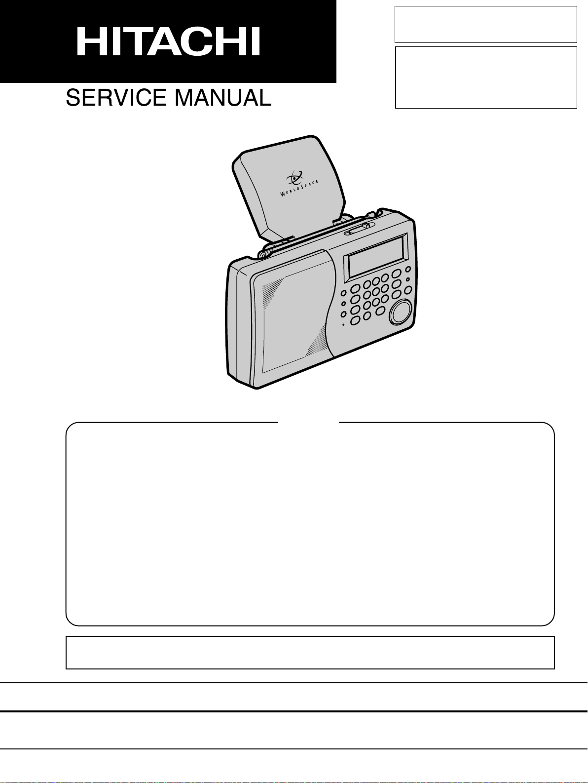
No. 0096E
KHWS1W
KHWS1WUN
CONTENTS
SPECIFICATIONS ..................................................................................................................................................... 2
SERVICE POINTS .....................................................................................................................................................3
ADJUSTMENTS ......................................................................................................................................................... 7
TROUBLESHOOTING ............................................................................................................................................... 10
BLOCK DIAGRAM OF ANTENNA AND TUNER UNIT............................................................................................17
DATA OF MICROPROCESSOR ...............................................................................................................................18
SEMICONDUCTORS ................................................................................................................................................. 24
WIRING DIAGRAM ....................................................................................................................................................30
PRINTED WIRING BOARD ....................................................................................................................................... 31
METHOD OF REMOVED IC ..................................................................................................................................... 36
CIRCUIT DIAGRAM ................................................................................................................................................... 37
BLOCK DIAGRAM ..................................................................................................................................................... 41
EXPLODED VIEW...................................................................................................................................................... 43
REPLACEMENT PARTS LIST ..................................................................................................................................45
This documentation is applied to rescrictions for management, export and supply to overseas based on the Wassenaar
Arrangement.
SPECIFICATIONS AND PARTS ARE SUBJECT TO CHANGE FOR IMPROVEMENT
November 1999
DIGITAL RECEIVER
HITACHI CONSUMER PRODUCTS (S)
Page 2
KH-WS1
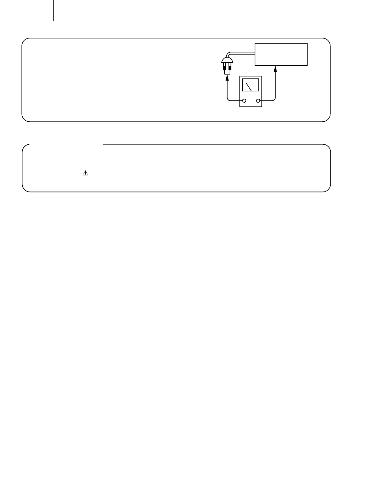
Check that exposed parts are acceptably insulated from
the supply circuit before returning the repaired instrument
to the customer.
INSTRUMENT
• Checking method
Measure the resistance value between the both poles of
attachment cup (Power supply plug) and the exposed
parts (Parts such as Knob, Cover, etc. where the customer is easy to touch.) and check that the resistance
value is 500 kohms or more.
Insulation tester (DC 500V)
(Exposed part)
SAFETY PRECAUTIONS
The following precautions should be observed when servicing.
1. Since many parts in the unit have special safety-related characteristics, always use genuine Hitachi’s replacement
parts. Especially critical parts in the power circuit block should not be replaced with other makers. Critical parts
are marked with in the circuit diagram and printed wiring board.
2. Before returning a repaired unit to the customer, the service technician must thoroughly test the unit to ascertain
that it is completely safe to operate without danger of electrical shock.
SPECIFICATIONS
• WS (WorldSpace digital broadcast) Section
Circuit system: Digital Receiver
Broadcast method: WorldStar 1 Method
Receiver frequency: L-Band (1453.384-1490.644 MHz)
Input/Output terminals
Antenna input terminal
Type/Impedance: F-type/50 Ω
Polarization voltage: LHCP 2.5-2.2 V
RHCP 3.3-2.8 V
Max. current supply: 70 mA
External terminal: 9-pin, for future expansion
WS antenna (Built-in, detachable type):
WorldStar 1 Method compatible
antenna
Gain: over 6 dBi
Dimensions: 150 x 33 x 156 mm
(w x h x d)
• Radio Section
Circuit system: FM/MW/SW1/SW2 4-bands
Superheterodyne
Tuning range: FM: 87.5 - 108 MHz
MW: 522 - 1620 kHz (9 kHz steps)
520 - 1620 kHz (10 kHz steps)
SW1:2.300-7.300 MHz
Meter band: 120, 90, 75, 60,
49, 41 m
SW2:9.500-26.100 MHz
Meter band: 31, 25, 21, 19, 16,
13, 11 m
Antennas: FM/SW1/SW2: Telescopic antenna
(aerial)
MW: Built-in ferrite-core antenna
(aerial)
• General Specifications
Power supply: AC: 110-127 V/220-240 V, 50/60 Hz
DC: 6 V
“D” cell or IEC R20 or equivalent x 4
(Optional)
DC input jack
Input voltage : DC 6 V + 30%,
–10% (DC 7.8 V – 5.4 V)
Current consumption: max. 400 mA
Power (mains) consumption: 5 W
Audio output: 3 W (PMPO)
300 mW (DC operation, 10% THD)
Speaker: 65 mm Cone/8 Ω
Output/Impedance: Headphones (stereo)/
Suitable impedance: 8-100 Ω
Line out (stereo)/2.2 kΩ
Battery life time: 30 hours over by using alkaline (LR20)
batteries.
12 hours over by using manganic
(R20P) batteries.
(Use HITACHI battery/Measured
method: EIAJ CP-2905A)
Dimensions: 240.5 x 162.5 x 64.5 mm
240.5 x 162.5 x 93 mm (w x h x d)
(including the WS antenna and handle)
Weight: 1.5 kg (without batteries),
1.9 kg (with batteries)
• Accessories
AC power cord: 1
AC plug adaptor: 1
F-type connector: 1 set (for making an extention coaxial
cable)
Waterproof cover: 1
Waterproof tape: 1
NOTE:
* Specifications are subject to change without notice.
– 2 –
Page 3

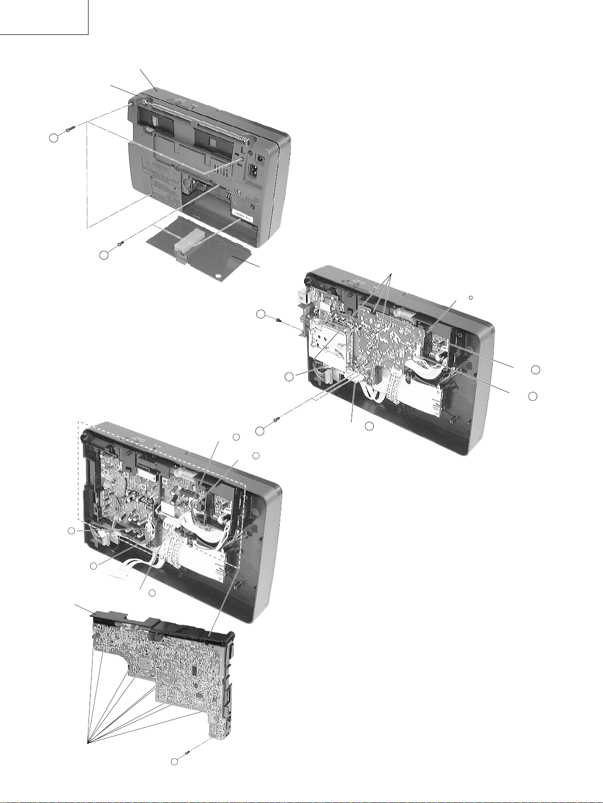
SERVICE POINTS
1. Removal of Back Case (Fig. 1)
(1) Remove 3 screws 1 from the back and 2 screws 2 inside the battery compartment.
(2) Detach the Antenna from the Ant }.
(3) Detach the connector A.
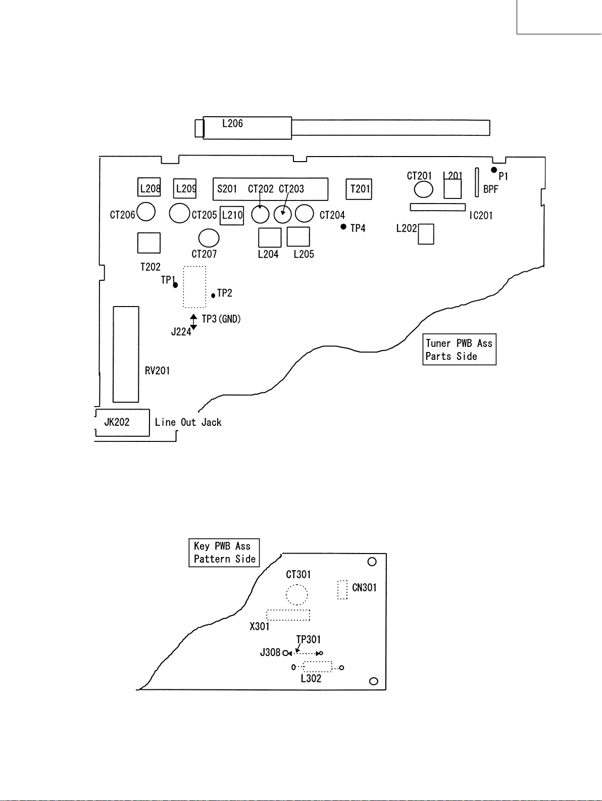
2. Removal of SATELLITE P.W.B. Board (Fig. 2)
(1) Detach all connectors B, C and D.
(2) Remove 1 screw 3 from the Satellite P.W.B. Board.
(3) Remove 2 screws 4 from the Satellite P.W.B. Board.
(4) Release the 3 catches and slide the Satellite P.W.B. Board away.
2. Removal of TUNER P.W.B. Board (Fig. 3)
(1) Detach 5 connectors E, F, G, H and I from the Tuner P.W.B. Board.
(2) Turn to the opposite side, remove 1 screw 5 from the Tuner P.W.B. Board.
(3) Detach 9 catches and separate the Tuner P.W.B. Board from the sub-chassis.
3. Removal of Insulator Pad (Fig. 4)
(1) Remove 6 screws 5 from the Insulator pad.
4. Removal of Main Board (Fig. 5)
(1) Remove 4 screws 6 from the Main Board.
KH-WS1
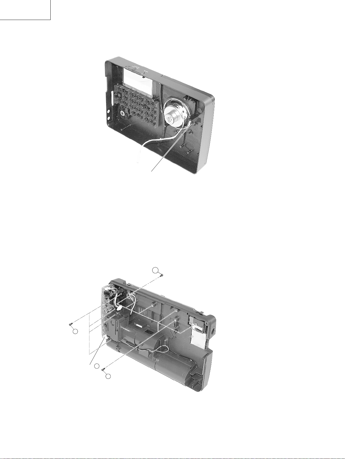
5. Removal of Speaker (Fig. 6)
(1) Release one end of the metal pin that secures the speaker position.
(2) Slide out the speaker.
6. Removal of POWER SUPPLY P.W.B. Board (Fig. 7)
(1) Remove 4 screws 7 and detach 1 connector J from the Power Supply P.W.B. board.
7. Removal of ANTENNA P.W.B. Board (Fig. 7)
(1) Remove 1 screw 9 from the Antenna P.W.B. board.
(2) Gently pull the Antenna P.W.B. board outwards.
8. Removal of WS ANTENNA SUPPORT PLATE (Fig. 7)
(1) Remove the 6 screws 8 and pull the WS Antenna Support Plate away from the Back case.
– 3 –
Page 4
KH-WS1
1
Fig. 1
Back case
2
Front case
Battery cover
3
3 Catches
Ant ·
Connector
Sub-Chassis
I
Connector
Connector
Connector
G
Connector
4
F
D
Connector
C
Connector
Connector
A
B
Fig. 2
H
E
Connector
9 Catches
Fig. 3
5
– 4 –
Page 5
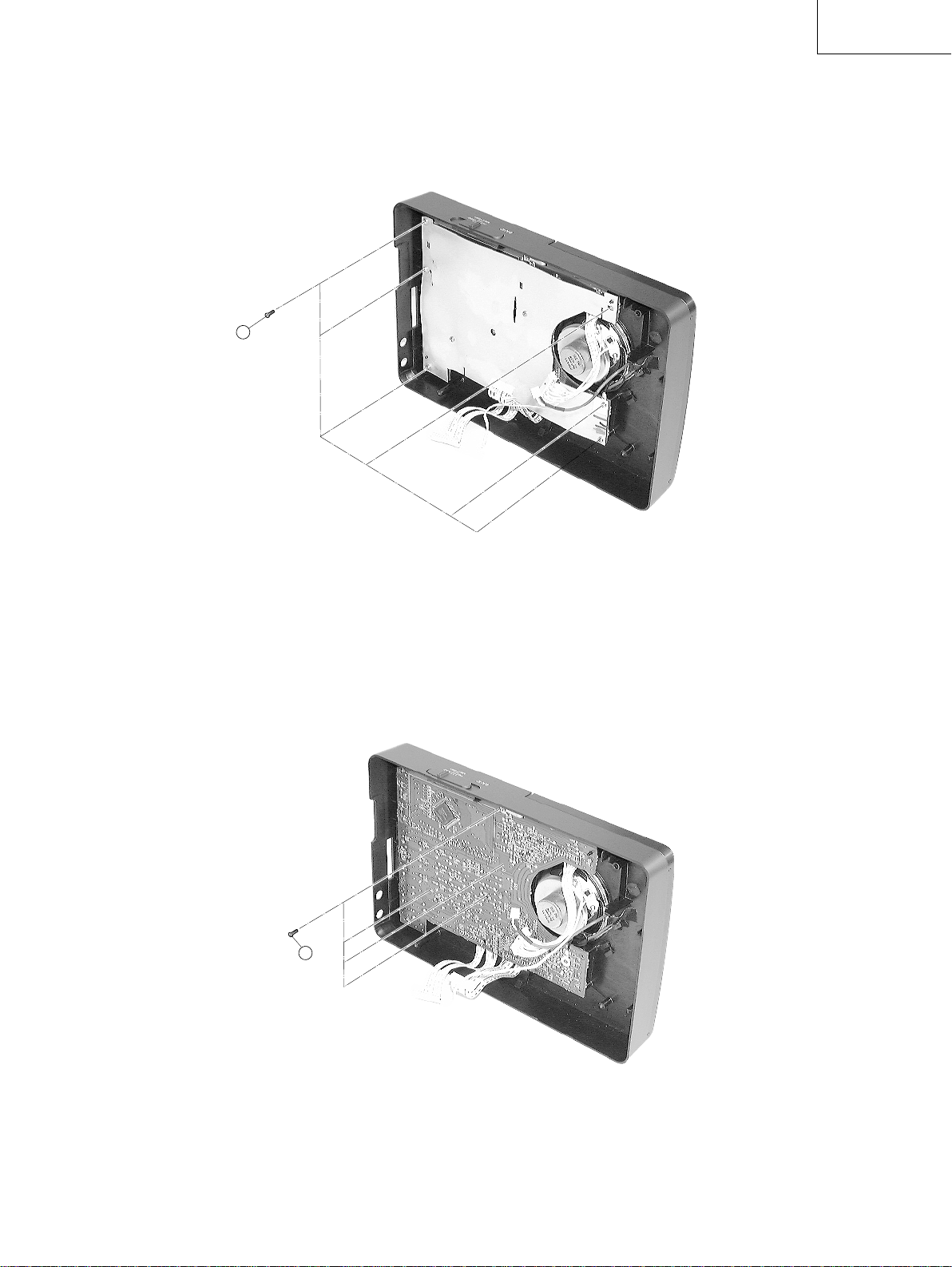
KH-WS1
5
Fig. 4
6
Fig. 5
– 5 –
Page 6
KH-WS1
metal pin
Fig. 6
9
7
Fig. 7
Connector
J
8
– 6 –
Page 7
KH-WS1
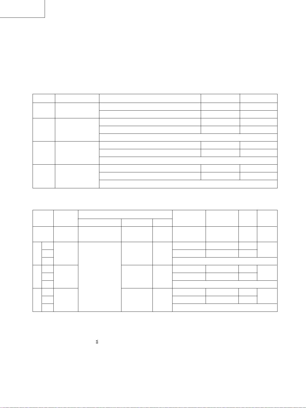
ADJUSTMENTS
• Adjustment points (Must adjust RADIO Part only. Adjustment on WS Part is not necessary.)
Remarks:
* After adjustment, should be fix following parts by Electro Wax.
"L201, L202, L206"
* After adjustment, do not touch the alighed components. (especially L201 and L202)
– 7 –
Page 8
KH-WS1
• Adjustments
(1) Before Adjustment
1) Set the Power SW to ON.
2) Set the Radio Function.
(2) Alignment for Tuning Capacitor Voltage Range (Covering)
1) Required Instruments
* Signal Generator
* DC volt meter
2) Alignment Procedure
* Connect a DC Volt meter to TP4 (J201)
Band Output Terminal
FM TP4
MW TP4
SW1 TP4
SW2 TP4
SG frequency & SET Tune Adjustment Reading
87.5 MHz L202 1.4 V ±0.1
108 MHz – 6 ~ 7.5 V
1) 520 kHz (10 kHz step)/522 kHz (9 kHz step) L210 1.2 V ±0.1
2) 1620 kHz CT207 7.2 V ±0.3
3) Repeat step 1-2
1) 2.3 MHz L208 1.1 V ±0.1
2) 7.3 MHz CT205 8.8 V ±0.3
3) Repeat step 1-2
1) 9.5 MHz L209 1.6 V ±0.1
2) 26.1 MHz CT206 9.0 V ±0.3
3) Repeat step 1-2
(3) Alignment for AM IF and MW, SW1, 2 Tracking
Step Item
1 AM IF
2 (1) MW Ant
(2)
(3)
3 (1) SW1 Ant
(2)
(3)
4 (1) SW2 Ant
(2)
(3)
Required Instrument & Connection
Instrument Input Output
Genescope (*1) Ferrite Ant.*2 TP1
AM signal generator F. Ant *2 TP1
400 Hz, 30% Mod.
ACVTM, oscillscope
MW: Note 2 P1 TP1
SW1,2: Note 5
P1 TP1
Remarks: Instrument Connection
*1: With a 470 µF/6.3 V capacitor to the TP2 (-) and J209/+B(+) "IC202".
*2: Mean Note 2 (See page 17)
Note: AM TRACKING ERROR SPEC
6dB.
Genescope or Receiving Adjust Reading
SG Freq. Freq. (Set)
450 kHz High end Freq. T202 Max.
Note 1
600/603 kHz 600/603 kHz L206 Max.
1400/1404 kHz 1400/1404 kHz CT204
Repeat steps (1) & (2)
3.2 MHz 3.2 MHz L205 Max.
7.1 MHz 7.1 MHz CT203
Repeat steps (1) & (2)
11.65 MHz 11.65 MHz L204 Max.
21.45 MHz 21.45 MHz CT202
Repeat steps (1) & (2)
– 8 –
Page 9
(4) Alignment for FM IF and FM Tracking
KH-WS1
Step Item
1IF
2(1) FM
(2)
(3)
Required Instrument & Connection
Instrument Input Output
Genescope IC201 TP1
FM signal P1 TP1
Generator
400 Hz, 22.5 kHz Dev
Note 6
Note:
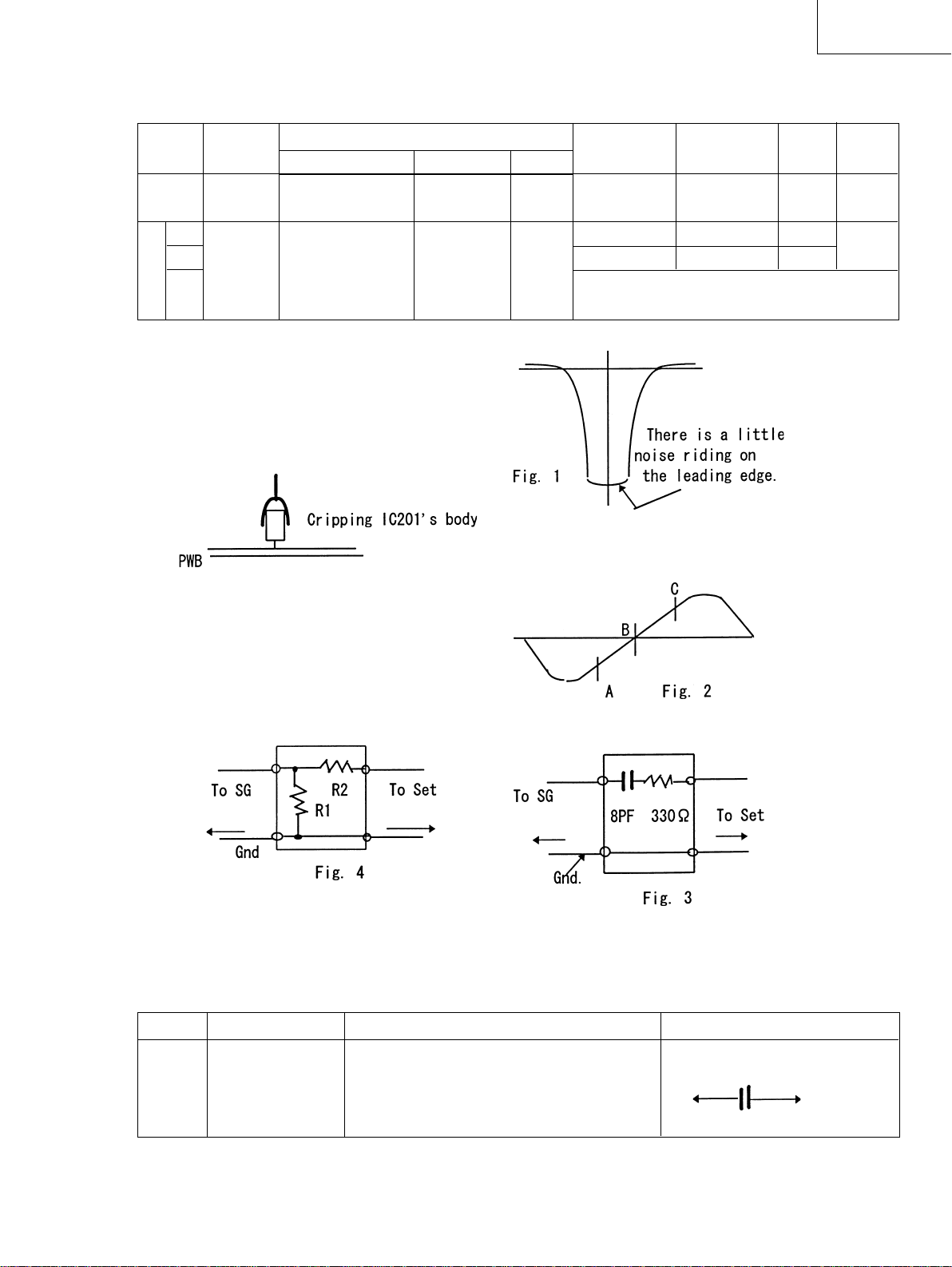
1. Feed in a week signal from the Genescope.
Adjust T202 for max. gain and the waveform
of Fig. 1.
2. Connect AM signal generator to loop antenna,
bring near to ferrite antenna.
3. Input signal methode as follows.
Note 3
Genescope or Receiving Adjust Reading
SG Freq. Freq. (Set)
10.7 MHz High End (or T201 Max.
106.1 MHz)Freq. Note 4
90.2 MHz 90.2 MHz L201 Max.
106.1 MHz 106.1 MHz CT201
Repeat steps (1) & (2)
4. Feed in a week signal to IC201 (Note 3) from the
genescope. Use the T201 core to from the Scurve shown in the Fig. 2.
Adjust the symmetry of A and B about point C for
linearity.
5. SW1, SW2 dummy antenna is shown in Fig. 3.
6. FM dummy antenna is shown in Fig. 4.
R1=Rg=SG's output impedance (75 Ω),
R2=75 - Rg/2
(5) Alignment for Clock Time Accuracy
Band Adjustment
FM CT301
Procedure Connection
1) Tune FM to 108 MHz
2) Connect a Freq. Counter to J308 To J308
3) Adjust CT301 to reach the frequency To Counter
118.7 MHz ±1.5 kHz
– 9 –
Page 10
KH-WS1
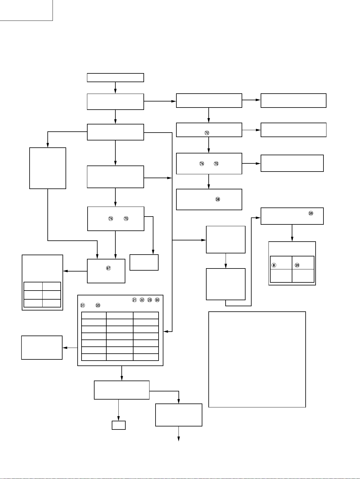
TROUBLESHOOTING
1. System Check
Connect to AC outlet.
Check IC301 control circuit.
Does the time
and "BATT"
displays appear
on the LCD,
then they
disappear after
2 seconds?
Yes
IC303 or Q303 is
broken down.
IC303 operation
V in
V out
>3.6V
<3.6V
H
L
Can the time display
appear?
No
Yes
Can the power SW turn
Yes
ON?
Yes
No
Can the power SW turn
ON after pressing the
Reset key?
Yes
No
Is the oscillator circuit of
IC301 and pin
in operation?
No
Yes
Does the port of
No
IC301 pin
operate in "H"?
(+3V)
Does every port of IC301 , , , ,
and pin operate on the following?
Check
IC301.
Is the voltage to the
Voltage Selector set correctly?
Yes
Is the voltage to
IC301 pin 3 V?
Yes
Is the oscillator circuit of
IC301 and pin in
operation?
Yes
Failure in the oscillator
circuit of IC302 pin for
the LCD driver or in IC302
Check "BATT"
display.
Is "BATT"
blinking on
the LCD?
Yes
Check the AC
voltage or replace
the battery in
case of battery
exhaustion.
No
No
No
Disconnect the power cord
and set the voltage correctly.
Check the +3 V line.
Check, the oscillator circuit
or IC301 is broken down.
Check whether IC301 pin
line is in "H" or not.
No
Check Q302, 307
and D318
CN302
<4.2V BATT
Pin
IC301
Pin
blinks.
Check around
IC301.
Is it broken down?
No
Pin No.
21
22
23
50
51
53
Is the LCD display
followed the right table?
OK
WS
H
H
L
H
H
H
Yes
Yes
RADIO
H
L
H
L
H
H
No
Check and follow
the flowchart for
each functions.
Proceed to each flowchart.
– 10 –
LCD display
Display when the power turns ON without
signal.
eg)
Check after resetting.
WS Function
WS SAT
/
SEARCH
/
AFRST - 1
/
Displaying "NO BEAM"
and the function
FM Function
FM 87.50MHz
Page 11
2. WS section
(1) Determine whether WS circuit malfunctions or communications to control microcomputer malfunction.
LCD Display
STEREO LOCKED
KH-WS1
B
WS Function
Is the display of part on LCD
followed on the following?
WS SAT
"SEARCH"
eg)
AFRST–1
– 1
*
NO BEAM
(when no signal
received)
At receiving
Is there any sound from
speakers even though the
display is correct?
Display
Broadcast name
(when any
signal received)
or
or
Ye s
No
No
Does only the part
of Function
display appear?
LCD display is abnormal
though any trouble is not
found in receiving
operation.
Are the operations
of terminal pins for
CN304 followed on the
table 1 when CN304 is
disconnected?
Ye s
A
C
Ye s
Ye s
No
WS S A T
(SC)
1
WS
LEVEL
Failure in IC301
or CN304
B
Figure 1
Ye s
Problem may in
WS circuit.
Proceed to item (2).
Table 1
PG304
CN304
10 L Clock signal 58 72
11 L L L 60 75
Power Off
(STANDBY)
1L H H55
2 (L) H H H 4 4
3 Clock signal 3 3
5 Clock signal 2 2
6 L L Clock signal 1 1
7H H H77
8 L L L 57 71
9 L Clock signal 59 74
Power On
(NO BEAM)
At receive
IC101 No.
64 Pin 80 Pin
– 11 –
Page 12
KH-WS1
(2) Checking and flowchart for WS circuit
Determine the display on LCD and the presence or absence of sound from speakers after turning the power ON.
Note: The terminal number of IC101is assumed 64-pin type in the flowchart. For 80-pin type, refer to tables 1 to 4 and note.
1 When no sound from speakers though any trouble is
not found in receiving and display
Start
Is any sound output from
speakers when changing the
mode into RADIO?
Ye s
WS
Function
Is IC103 pin clocked in
at 14.725 MHz
Ye s
Ye s
Are IC102 , , , pin
and IC103 , , , pin
followed the table 3?
Is IC103 pin clocked
out at 24.576 MHz and
clocked into IC102 pin?
Are the operations of IC103
and pin followed the
table 4?
Check the audio circuit
No
around IC206, IC207,
No
Check R155 and
around IC103 pin.
No
Check every port of
IC102 and IC103.
Check around IC102
No
pin and IC103 pin,
IC103 may malfunction.
No
Check around IC103,
IC103 may malfunction.
and IC210.
2 When no operation goes on
Only the part C of figure 1 or abnormal display will appear
on LCD.
Start
Check whether IC301
, and pin are in "H"
or not.
Ye s
Is the oscillator circuit of
IC101 and pin
in operation?
Note : 80 Pin
Type nos. and
IC101 No.
64 Pin
28
29
30
32
33
41
42
43
46
47
80 Pin
36
37
38
40
41
52
53
54
58
59
Power Off
(STANDBY)
No
Is any clock signal found in
IC101 and pin?
Ye s
No
Power On
(NO BEAM)
L
H
L
L
HL
L
HHL
L
L
L
L
L
L
L
L
L
L
HL
HL
Check the terminals
of PG304 to IC101,
IC101 may malfunction.
No
Check the oscillator
circuit or IC101 may
be in failure.
At receive
(reset)
(reset)
(reset)
L
Sync Pulse
Data signal
Clock signal
Data signal
(reset)
(reset)
H
H
H
H
H
H
Connect to
another IC
IC102
27
21
26
25
24
28
20
Table 2
IC103
7
41
40
39
2
IC102
No.
30
31
32
33
Power Off
(STANDBY)
L
L
L
L
Power On
(NO BEAM)
L
L
L
24 kHz
At receive
Clock signal
Data signal
Digital audio data
8 kHz
Table 3
Connect to
another IC
IC103 No.
32
30
25
24
– 12 –
IC102
No.
16
22
23
27
33
Power Off
(STANDBY)
L
L
L
L
L
Power On
(NO BEAM)
L
L
L
H
L
At receive
(Sync puls)
HL
(Sync puls)
HL
H
L
H
Table 4
Connect to
IC 101 No.
64 Pin 80 Pin
27
26
25
24
23
35
33
32
30
28
Page 13
3 When the operation malfunctions after receiving operation starts
Display of part on LCD:
WS SAT
or or
Continue blinking
of "SEARCH"
NO BEAM
"SEARCH"
KH-WS1
Receiving
operation
"SEARCH"
etc.
Is the oscillator circuit of
IC102 - and -pin in
operation?
or
Can I2C bus line connected from
IC101 - and -pin to all ICs
operate? (80 pin nos. and )
or
Are IC101 -pin and IC102
-pin in "H"?
or
Is every port connected from
IC101 -pin to IC102 and
IC103 in "H"?
When the stations receivable with other units can not be received though the operation is proper
4 When the stations receivable with other units can not be received though the operation is proper
Start
No
No No
No
No
Is the synchronous pulse "H L"
repeated at IC103 -pin?
or
Does IC103 -pin operate
in "L"?
Check the circuits connected to
each IC terminals, the patterns
and the soldered parts, the
concerned IC may malfunction.
No
Check around the
terminals of IC103
and IC101.
Execute "SEEK" Search.
Push MODE and BEAM SEEK keys.
Can IC101 -pin switch "H to L"
after starting SEEK until it ends?
(80 pin: )
Ye s
Does the voltage for RF101 (Tuner) -pin
change from 3 V to 2.4 V when SEEK
search until it ends?
Ye s
Is there voltage output between the center pin
and the ground of the antenna jack on the unit
when the antenna is disconnected?
Does the voltage change from 3 V to 2.4 V
when SEEK search until it ends?
Ye s
No
No
No
Check IC101.
Check IC105 and
IC106.
Check the output line of
IC105 and IC106, and
around the terminals of RF101.
– 13 –
Check the output line of
IC105 and IC106, and
around the terminals of RF101.
Page 14

No
1
2
3
4
5
6
7
8
9
10
IC101 47Pin
(80pin No: 59)
IC101 28Pin
(80pin No: 36)
IC101 32Pin
(80pin No: 40)
IC101 46Pin
(80pin No: 58)
IC102 12Pin
(80pin No: 16)
IC101 29Pin
(80pin No: 37)
IC101 35, 36Pin
(80pin No: 43, 44)
IC101 30Pin
(80pin No: 38)
IC101 33Pin
(80pin No: 42)
IC101 35, 36Pin
(80pin No: 43, 44)
IC102 20pin
IC103 2pin
IC103 7pin
IC103 39pin
IC102 28pin
IC103 43pin
WS TUNER 8pin
IC103 41pin
IC102 22, 23pin
IC102 27pin
IC103 40pin
IC102 21pin
IC102 22, 23pin
IC terminal no.
IC function / I/O Data Connect to
Check to confirm operation
WS RESET/Output Reset IC102 and IC103.
DCEN/Output
PUP IN/Input
PUP OUT/Output
Clock 14.725 MHz/Output
WRDY/Input
I
2
C BUS / I/O
WSEN/Input
SYNC/Input
I
2
C BUS / I/O I
2
C BUS communication
I
2
C BUS communication
Clock waveform
Turn IC103 on.
Make sure IC103 is turned on.
Turn IC102 on.
IC103 generates 24.576 MHz from this clock
(14.725MHz) for 38-pin out.
IC103 outputs a verification signal for the
clock receiving.
Set each IC to WS mode.
IC101 inputs a verification signal that IC102 has
been in WS mode.
IC102 responds that TSCC data has been
received in WS mode.
Microcomputer reads out the received TSCC
data from IC102.
(3) Operations on WS functions after turning the power on
KH-WS1
– 14 –
Page 15

3. Check IC 24LC194 (IC107, E2 PROM) of WS function
Check the following after turning the
power ON with displays on LCD or key operations.
Will the LCD display change
as follows?
When there is no signal
WS SAT
e g)
AFRST – 1 or
AFRST – 1
*
"SEARCH"
(Frashing)
Does the display followed
"WS SAT" on LCD become
one of next cases?
Case 1 Case 2
The next display is
not appeared on
LCD.
The next operation
does not go on with
"SEARCH" blinks.
KH-WS1
Case 3
Description of LCD display
Push MODE Key Turn on light "MODE"
Press it successively.
Push PASSWORD Key
Press it secondly.
"PASSW – 01"
NO BEAM
OK
Check IC107, it may
be in failure.
When it can
not operate
Push PASSWORD Key
Press it thirdly.
Push PASSWORD Key
LCD display
First half ID
number always
"00000000"
Press SC Up key.
LCD display
Second half ID
"00001234"
OK
"PASSW – 02"
"ID"
The ID number is displayed on
LCD after 2 seconds.
If "1234"
– 15 –
Page 16

KH-WS1
4. Radio Section
RADIO Function
Is the key
operations ok?
Ye s
Can each sound of
bands switched and
output?
Ye s
IC301 is in normal
operation. Check other
circuits for RADIO parts.
Cause of malfunction
Are the voltages for
No
PG302 - and -pin
followed on the table 6
when CN302
is disconnected?
Ye s
Check the
circuits G
and H of
S201.
Input port operations of IC301 - and -pin
( Pg
302 – 4 )
( Pg
302 – 5 )
Check IC301.
FM MW SW1 SW2
LH L H
LL H H
No
No
Is the voltage for Q219 collector followed
on the next table when its frequency is up
and down (High end/Low end frequency)?
FM 1. 3 – 1. 4
MW
SW1
SW2
Table 6
Check the operations of - to
-pin and the voltage for key
operation. (Table 5)
Is the LCD display correct if
No
bands are switched each
other?
Q219 collector
Low freq.
1. 1 – 1. 2
1. 0 – 1. 1
1. 5 – 1. 6
Can the indication
of "LOCKED" light?
Check the audio
circuits of IC205,
IC206, IC207 and
IC210.
Ye s
6. 0 – 7. 5
7. 2 – 7. 3
8. 8 – 8. 9
9. 0 – 9. 1
Ye s
High freq.
No
Voltages for IC301 -, - and -pin at
key operations
42 43 44 Voltage (V)
1 7 MEMORY 0.3
2 8 METER 0.8
3 9 WS/RADIO 1.3
40 PTY1.8
5 ST/MONO LANG 2.3
6 BACKS SLEEP 2.8
No
Is the voltage for
IC203 -pin
15 V?
Ye s
Does the local
oscillator work at
IC301 -pin of
Q301 connector
in FM mode, and
at IC202 -pin
and IC301 -pin
in AM mode?
Ye sYe s
Check the line of
IC301 -pin or
the circuits of
Q218 and Q219.
No
No
Ye s
Check IC203 or
L214.
FM : IC201
Q301,
CN301,
D204
AM : IC202
D206,
Check above.
Ta b l e 5
Check IC202 and
Q201 to Q203.
– 16 –
Failure in
IC301
Page 17

BLOCK DIAGRAM OF ANTENNA AND TUNER UNIT
• Antenna Unit (RF001)
KH-WS1
• Tuner Unit (RF101)
– 17 –
Page 18

KH-WS1
DATA OF MICROPROCESSOR
1 In case 64 PIN type
HD6472128FA20 or
HD6432127RWV03FA
• Terminal Function
Pin
Symbol I/O Function
No.
1 P50/TxD0 O Signal data output
2 P51/RxD0 I Signal data input
3 P52/SCK0 I / O Clock input/output
4 RES I When this pin is driven low, the chip is
5 NMI I WS POWER ON (Wake Up) signal
6 VCC – +3.3 ∇ power supply
7 STBY I When this pin is driven high, hardware
8 VSS – Ground
9 XTAL – 8.00 MHz Ceramic Oscillator connect
10 EXTAL – 8.00 MHz Ceramic Oscillator connect
11 MD1 I Mode pins setting to “H”
12 MD0 I Mode pins setting to “H”
13 AVSS – Analog Ground
14 P70/AN0 I Not used, setting to “L”
15 P71/AN1 I WS POWER ON (Wake Up) signal
16 P72/AN2 I Not used, setting to “L”
17 P73/AN3 I Not used, setting to “L”
18 P74/AN4 I Not used, setting to “L”
19 P75/AN5 I Not used, setting to “L”
20 P76/AN6 I Not used, setting to “L”
21 P77/AN7 I Not used, setting to “L”
22 AVCC – +3.3 ∇ analog power supply
23 P60 I MPEG-FRAME-Sync signal input
24 P61 I MPEG-CRC-ERROR signal input
25 P62 I MPEG-BC-Sync signal input
26 P63 I BC-FRAME-Sync signal input
27 P64 I BC-FRAME-Toggle signal input
28 P65 O DCEN signal output
29 P66 I Ready signal input
30 P67 O Enable signal input
31 VCC – +3.2 ∇ power supply
reset
input
standby signal
input
Pin
Symbol I/O Function
No.
32 P27 I Power up signal input
33 P26 I Sync signal input
34 P25 I Not used, setting to “L”
35 P24/SCL1 O I2C Serial bus line “clock”
36 P23/SDA1 O I2C Serial bus line “data”
37 P22 O Not used, setting to “L”
38 P21 O Not used, setting to “L”
39 P20 O Not used, setting to “L”
40 VSS – Ground
41 P17 O Not used pin
42 P16 O Not used pin
43 P15 O Not used pin
44 P14 – Not used, setting to “L”
45 P13 O
46 P12 O Power up signal output
47 P11 O Reset signal output
48 P10 I Not used
49 P30 I Fixing to “H”
50 P31 I Not used, fixing to “L”
51 P32 I Not used, fixing to “L”
52 P33 I Not used, fixing to “L”
53 P34 I Not used, fixing to “L”
54 P35 I Not used, fixing to “L”
55 P36 I Not used, fixing to “L”
56 P37 I Not used, fixing to “L”
57 P40/IRQ2 I STRB. signal input from Tuner µcon
58 P41/IRQ1 O STRB. signal output to Tuner µcon
59 P42/IRQ0 I ACK. signal input from Tuner µcon
60 P43 O ACK. signal output to Tuner µcon
61 P44 I Not used
62 P45 O WS Audio mute signal output
63 P46 I Not used
64 P47 O Not used
L/R HCP change signal output LHCP = “L”
– 18 –
Page 19

2 In case 80 PIN type
HD6472128TF20
• Terminal Function
KH-WS1
Pin
Symbol I/O Function
No.
1 P50/TxD0 O Signal data output
2 P51/RxD0 I Signal data input
3 P52/SCK0 I / O Clock input/output
4 RES I When this pin is driven low, the chip is
5 NMI I WS POWER ON (Wake Up) signal
6 VCC – +3.3 ∇ power supply
7 STBY I When this pin is driven high, hardware
8 VSS – Ground
9 VSS – Ground
10 VSS – Ground
11 XTAL – 8.00 MHz Ceramic Oscillator connect
12 VSS – Ground
13 EXTAL – 8.00 MHz Ceramic Oscillator connect
14 MD1 I Mode pins setting to “H”
15 VSS – Ground
16 MD0 I Mode pins setting to “H”
17 AVSS – Analog Ground
18 P70/AN0 I Not used, setting to “L”
19 P71/AN1 I WS POWER ON (Wake Up) signal
20 P72/AN2 I Not used, setting to “L”
21 P73/AN3 I Not used, setting to “L”
22 P74/AN4 I Not used, setting to “L”
23 P75/AN5 I Not used, setting to “L”
24 VSS – Ground
25 P76/AN6 I Not used, setting to “L”
26 P77/AN7 I Not used, setting to “L”
27 AVCC – +3.3 ∇ analog power supply
28 P60 I MPEG-FRAME-Sync signal input
29 VSS – Ground
30 P61 I MPEG-CRC-ERROR signal input
31 VSS – Ground
32 P62 I MPEG-BC-Sync signal input
33 P63 I BC-FRAME-Sync signal input
34 VSS – Ground
35 P64 I BC-FRAME-Toggle signal input
36 P65 O DCEN signal output
37 P66 I Ready signal input
38 P67 O Enable signal input
39 VCC – +3.2 ∇ power supply
reset
input
standby signal
input
Pin
Symbol I/O Function
No.
40 P27 I Power up signal input
41 P26 I Sync signal input
42 P25 I Not used, setting to “L”
43 P24/SCL1 O I2C Serial bus line “clock”
44 P23/SDA1 O I2C Serial bus line “data”
45 VSS – Ground
46 P22 O Not used, setting to “L”
47 P21 O Not used, setting to “L”
48 P20 O Not used, setting to “L”
49 VSS – Ground
50 VSS – Ground
51 VSS – Ground
52 P17 O Not used pin
53 P16 O Not used pin
54 P15 O Not used pin
55 VSS – Ground
56 P14 – Not used, setting to “L”
57 P13 O
58 P12 O Power up signal output
59 P11 O Reset signal output
60 P10 I Not used
61 P30 I Fixing to “H”
62 P31 I Not used, fixing to “L”
63 P32 I Not used, fixing to “L”
64 P33 I Not used, fixing to “L”
65 P34 I Not used, fixing to “L”
66 VSS – Ground
67 P35 I Not used, fixing to “L”
68 P36 I Not used, fixing to “L”
69 P37 I Not used, fixing to “L”
70 VSS – Ground
71 P40/IRQ2 I STRB. signal input from Tuner µcon
72 P41/IRQ1 O STRB. signal output to Tuner µcon
73 VSS – Ground
74 P42/IRQ0 I ACK. signal input from Tuner µcon
75 P43 O ACK. signal output to Tuner µcon
76 VSS – Ground
77 P44 I Not used
78 P45 O WS Audio mute signal output
79 P46 I Not used
80 P47 O Not used
L/R HCP change signal output LHCP = “L”
– 19 –
Page 20

KH-WS1
DRD3515A-QG-E3
(IC102)
• DRD3515A Terminal Function
Pin No.
QFP
1 AGNDC BID Analog reference ground
2 AVSS1 SUPPLY Analog ground for audio stages
3 AVSS0 SUPPLY Analog ground for audio output amplifiers
4 OUT1 OUT Not used
5 OUT2 OUT Not used
6 AVDD0 SUPPLY Power supply for audio output amplifiers
7 AVDD1 SUPPLY Power supply for audio stages
8 XTI IN 14.725 MHz quartz oscillator pin 1
9 XTO OUT 14.725 MHz quartz oscillator pin 2
10 AVDD2 SUPPLY VDD for IF input
11 AVSS2 SUPPLY VSS for IF input
12 RCLK OUT Output reference frequency
13 SGND IN Signal GND for IF input
14 IFIN IN Differential IF input
15 IFINQ IN Differential IF input inverted
16 VREFI BID Reference for IF input
17 VSS SUPPLY Digital VSS
18 VDD SUPPLY Digital VDD
19 TEQ IN “H” digital VDD
20 PORQ IN Power On Reset, active low
21 SYNC OUT TSCC mode : TSCC data ready
22 SDA BID I2C Data Line
23 SCL BID I2C Clock Line
24 SCC OUT Service Component Clock
25 SCD OUT Service Component Data
26 SBCW OUT Service Component Wordstrobe
27 WSEN OUT WorldSpace enable output
28 PUP IN Power up
29 OCLK IN 24.576 MHz input oversampling clock
30 BCC OUT Broadcast Channel clock
31 BCD OUT Broadcast Channel data
32 DAI IN Digital Audio Frame Identification
33 DAD IN Digital Audio Data
34 AUX2L IN AUX2 left input for external analog signals (not used)
35 AUX2R IN AUX2 right input for external analog signals (not used)
36 AUX1L IN AUX1 left input for external analog signals (not used)
37 AUX1R IN AUX1 right input for external analog signals (not used)
38 FOUTL OUT Output to left external filter
39 FOPL BID Filter op-amp inverting input, left
40 FINL OUT Filter op-amp output (line out)
41 FOUTR OUT Output to right filter op-amp
42 FOPR BID Right filter op-amp inverting input
43 FINR OUT Filter op-amp output (line out)
44 VREF IN Analog reference voltage
Pin Name Type Description
BC mode : Decryption data from new
SCH available
– 20 –
Page 21

MAS3506D-QG-E9
(IC103)
• DRD3515A Terminal Function
KH-WS1
Pin No.
QFP
1 TE I Test Enable / Not used / Connected to Ground
2 PORQ I Power ON RESET, Active Low
3 I2CC I O I2C Clock Line
4 I2CD I O I2C Data Line
5 VDD SUPPLY Power Supply for Digital Parts (+3.2 ∇)
6 VSS SUPPLY Ground Supply for Digital Parts
7 DCEN I Voltage Supervision
8 EOD O Not used
9 RTR O Not used
10 RTW O Not used
11 DCSG SUPPLY Ground
12 DCSO O Open Drain “L” / Not used
13 VSENS I DC Converter Voltage Sense
14 PR I PIO DMA Request or Read/Write
15 PCS I PIO Chip Select, Active Low
16 PI19 O BC-Frame-Toggle
17 PI18 I BCINENABLEQ
18 PI17 I PIO Data [17], reserved
19 SIC* I PIO Data [16] (SIC*)
20 SII* I PIO Data [15] (SII*)
21 SID* I PIO Data [14] (SID*)
22 PI13 O MPEG-FRAME-SYNC
23 PI12 O BC-SYNC
24 SOD O Serial Output Data
25 SOI O Serial Output Frame Identification
26 SOC O Serial Output Clock
27 PI8 O MPEG-CRC-Error
28 XVDD SUPPLY Positive Supply of Output Buffers
29 XVSS SUPPLY Ground of Output Buffers
30 SID I Serial Input Data
31 SII I Serial Input Frame Identification
32 SIC I Serial Input Clock
33 PI4 O MPEG-FRAME-SYNC
34 PI3 I AUD-SW, information from headphone jack
35 PI2 I Reserved
36 PI1 I Reserved
37 PI0 I Reserved
38 CLKO O Clock Output (nominal 24.576 MHz)
39 PUP O Power Up, i.e. Status of Voltage Supervision
40 WSEN I WS Enable : Enable Layer 3 Decoding
41 WRDY O WSEN = 0 : Valid clock input at CLKI
42 AVDD SUPPLY Supply for Analog Circuits
43 CLKI I Clock Input
44 AVSS SUPPLY Ground Supply for Analog Circuits
Pin Name Type Description
WSEN = 1 : Clock synthesizer locked to Broadcast Channel data stream
– 21 –
Page 22

KH-WS1
TC9327F-200 or -800
(IC301)
• Terminal Function
Pin
No.
1 COM 1 OUT Not used
2 COM 2 OUT Not used
3 COM 3 OUT Not used
4 COM 4 OUT Not used
5 S 1 OUT Not used
6 S 2 OUT Not used
7 S 3 OUT Not used
8 S 4 OUT Not used
9 S 5 OUT Not used
10 S 6 OUT Not used
11 S 7 OUT Not used
12 S 8 OUT Not used
13 S 9 OUT Not used
14 S 10 OUT Not used
15 S 11 OUT Not used
16 S 12 OUT Not used
17 S 13 OUT Not used
18 S 14 OUT Not used
19 S 15 OUT Not used
20 S 16 OUT Not used
21 AUDIO OUT Function Output
22 WS OUT
23 RADIO OUT
Terminal I/O Function
Port output will be set as the following table according to the
currently received function.
OFF WS RADIO
AUDIO L H H
WS L H L
RADIO L L H
24 N.C. OUT Not used
25 BAND 0 IN Band Input
26 BAND 1 IN
27 BAND 2 IN
Set port input as the following table in accordance with the currently
receiving band.
BAND 0 L H L H
BAND 1 L L H H
BAND 2 L L L L
FM MW SW1 SW2
– 22 –
Page 23

KH-WS1
Pin
No.
28 N.C. OUT Not used
29 T7 (P9-0) OUT
30 T6 (P9-1) OUT KEY TIMING O/P TERMINAL
31 T5 (P9-2) OUT
32 T4 (P9-3) OUT Not used
33 N.C. OUT Not used
34 K0 (KEY IN) IN
35 K1 (KEY IN) IN
36 K2 (KEY IN) IN
37 K3 (KEY IN) IN
38 T0 (P1-0) OUT
39 T1 (P1-1) OUT KEY TIMING O/P TERMINAL
40 T2 (P1-2) OUT
41 T3 (P1-3) OUT Not used
42 AD IN 1 IN
43 AD IN 2 IN KEY I/P TERMINAL
44 AD IN 3 IN
45 DCREF IN Not used
46 SDR (SI) IN SERIAL DATA I/P TERMINAL
47 SDATA (SO) OUT SERIAL DATA O/P TERMINAL
48 SCK OUT SERIAL LOCK O/P TERMINAL
49 CE (LCD) OUT
50
51 WS RESET OUT WS RESET O/P TERMINAL
52 N.C. OUT Not used
53 WS STBY OUT WS STBY O/P TERMINAL
54 DTS STB OUT
55 DTS ACK OUT
56 M STB IN
57 M ACK IN
58 ST IN IN STEREO I/P
59 BATTERY IN IN BATTERY REMAINING I/P
60 ST/MONO OUT STEREO/MONO O/P
61 SD IN IN
62 MUTE OUT MUTING O/P H : MUTE L : OFF
63 TEST IN Not used
64 IF IN IN IF SIGNAL I/P TERMINAL
65 PLL OUT OUT PLL O/P TERMINAL
66 PLL OUT OUT PLL O/P TERMINAL
67 HOLD IN IN BACKUP MODE CANCELLING
68 LIGHT OUT LIGHT O/P (Not used)
69 GND — GND TERMINAL
70 FM IN IN FM OSC input
71 AM IN IN AM OSC input
72 VDD — +3.0 ∇ power supply
73 RESET IN
74 XOUT — 75 kHz X’tal oscillator connect
75 XIN — 75 kHz X’tal oscillator connect
76 VXT — POWER FILTER TERMINAL
77 VLCD — Connect to VDD
78 C1 — Not used
79 C2 — Not used
80 VEE — Not used
Terminal I/O Function
KEY I/P TERMINAL
LCD CHIP ENABLE O/P TERMINAL
WS ON (POWER)
OUT WS ON O/P TERMINAL
DTS CHIP ENABLE O/P TERMINAL
DTS ACKNOWLEDGE O/P TERMINAL
MICON CHIP ENABLE I/P TERMINAL
MICON ACKNOWLEDGE I/P TERMINAL
ST DETECTION I/P L : DETECTED
SYS RESET SIGNAL I/P TERMINAL
Connect to VDD
– 23 –
Page 24

KH-WS1
SEMICONDUCTORS
IC’s
•
PCF8574AT (IC104)
24LC194 (IC107)
PCF8574AT Terminal Function
Pin
No.
1 (AO) Address input 0 not used fixed “H”
2 (A1) Address input 1 not used fixed “H”
3 (A2) Address input 2 not used fixed “H”
4 (P0) CLK Quasi-bidirectional I/ O 0
5 (P1) DATA Quasi-bidirectional I /O 1
6 (P2) EN Quasi-bidirectional I / O 2
7 P3 Quasi-bidirectional I / O 3
8 VSS Supply ground
9 (P4) Quasi-bidirectional I/ O 4 not used
10 (P5) Quasi-bidirectional I / O 5 not used
11 (P6) Quasi-bidirectional I / O 6 not used
12 (P7) Quasi-bidirectional I / O 7 not used
13 (INT) Interrupt output (active low) not used
14 SCL Serial clock line
15 SDA Serial data line
16 VDD Supply voltage
Symbol Description
Pin Function
Name Function
VSS Ground
SDA Serial Address/Data I/ O
SCL Serial Clock
WP Write Protect Input
VCC +3.2 ∇ Power Supply
NC No Internal Connection Fixed “L”
Block Diagram
– 24 –
Page 25

TA7358AP (IC201)
1
TA8132AF (IC202)
KH-WS1
9
24
1
TA8126F (IC203)
10
1
12
5
BA4510F (IC205, 210)
8
4
1
– 25 –
Page 26

KH-WS1
TA7368P (IC206, 207)
9
1
BU4066BCF (IC204)
114
78
BA033ST-V5 (IC209)
5
4
3
2
1
– 26 –
Page 27

MM1385D (IC208)
C01
OPI
VCC
OUT
GND
N.C.GND
5
4
3
12
(SUB)
MM1385H (IC105)
MM1385P (IC106)
V
in
5 4
KH-WS1
V
out
1
5
2
3
4
PST9136N (IC303)
Noise
Cont.
Gnd
3
1
Thermal
Protect
2
5
1
2
4
3
– 27 –
Page 28

KH-WS1
TC9298F (IC302)
– 28 –
Page 29

DIODES (including LED)
2
1
1: D Drain
2: G Gate
3: S Source
3
•
KH-WS1
1N4531
Black
1SS355
FM4002
A
TRANSISTORS
•
C
White
1SS133 1N4001 MTZ-J3.6B
Yellow
1SV149
Silver
RB461F SLR56VC3F (RED)
Navy Blue
1SV101
C
A
A
Cathode
Anode
C
HIT9016G 2SA1020 (Y) 2SK242
B Base
C Collector
E Emitter
2SC2412K
2SA1037AK (Q/R)
B Base
C Collector
E Emitter
DTC124EK
DTA144GKA
2SD1757K (Q/R)
2SD1048
3
2
1
1: E Emitter
2: B Base
3: C Collector
2
3
1
1: E GND/Emitter
2: B IN/Base
3: C OUT/Collector
1N4531
B
DTC124EK
1N4531
22 kΩ
22 kΩ
C
E
C
– 29 –
B
DTA144GKA
47 kΩ
E
Page 30

KH-WS1
ANT PWB
W001
(MX)
CN204
(MX)
CN002
(MX)
PG002
(MX)
PG301
(MX)
PG303
(MX)
PG302
(PH)
PG202 (PH)
CN301 (MX)
Shield
Sheet
White
CN302
(PH)
CN303
(MX)
CN304
(TXL)
W302
SP001
PG201
(PH)
PG204
(PH)
PG304
(TXL)
PG203
(PH)
TUNER
FRONT END
RF101
H.P PWB ASS
LCD
DISPLAY PWB ASS
(pattern side view)
JK101
CN203
(PH)
CN201(PH)
IC201
S201
SAT. PWB ASS
L206 (FERRITE ANT)
TUNER PWB ASS
CT204
ø1.0
Terminal
DC
J
CN001
BATT CASE
BLK
Twisted
ORG
Z001
Add manual
solder
Battery spring
Solder after 1~2T
Winding of conductor part
to battery spring
CAUTION: Do not drop solder inside
speaker or produce solder
spikes when soldering this wire.
3
1
2
1
1~2T Winding of
insulation part
AC
INLET
PS PWB ASS
P, T
Non colour
Bend wire
before
insertion
Bend wire
before
insertion
BLK RED
Gnd
Blue
L2
L1
–
+
WIRING DIAGRAM
– 30 –
Page 31

PRINTED WIRING BOARD
Soldering Side
HEADPHONE PWB
KH-WS1
Component Side
ANTENNA PWB
POWER SUPPLY PWB
– 31 –
Page 32

KH-WS1
Soldering Side
Soldering Side
SATELLITE P.W.B.
TUNER PWB
– 32 –
Page 33

Component Side
KH-WS1
Component Side
SATELLITE P.W.B.
TUNER PWB
– 33 –
Page 34

KH-WS1
Soldering Side
MAIN PWB
– 34 –
Page 35

Component Side
KH-WS1
MAIN P.W.B.
– 35 –
Page 36

KH-WS1
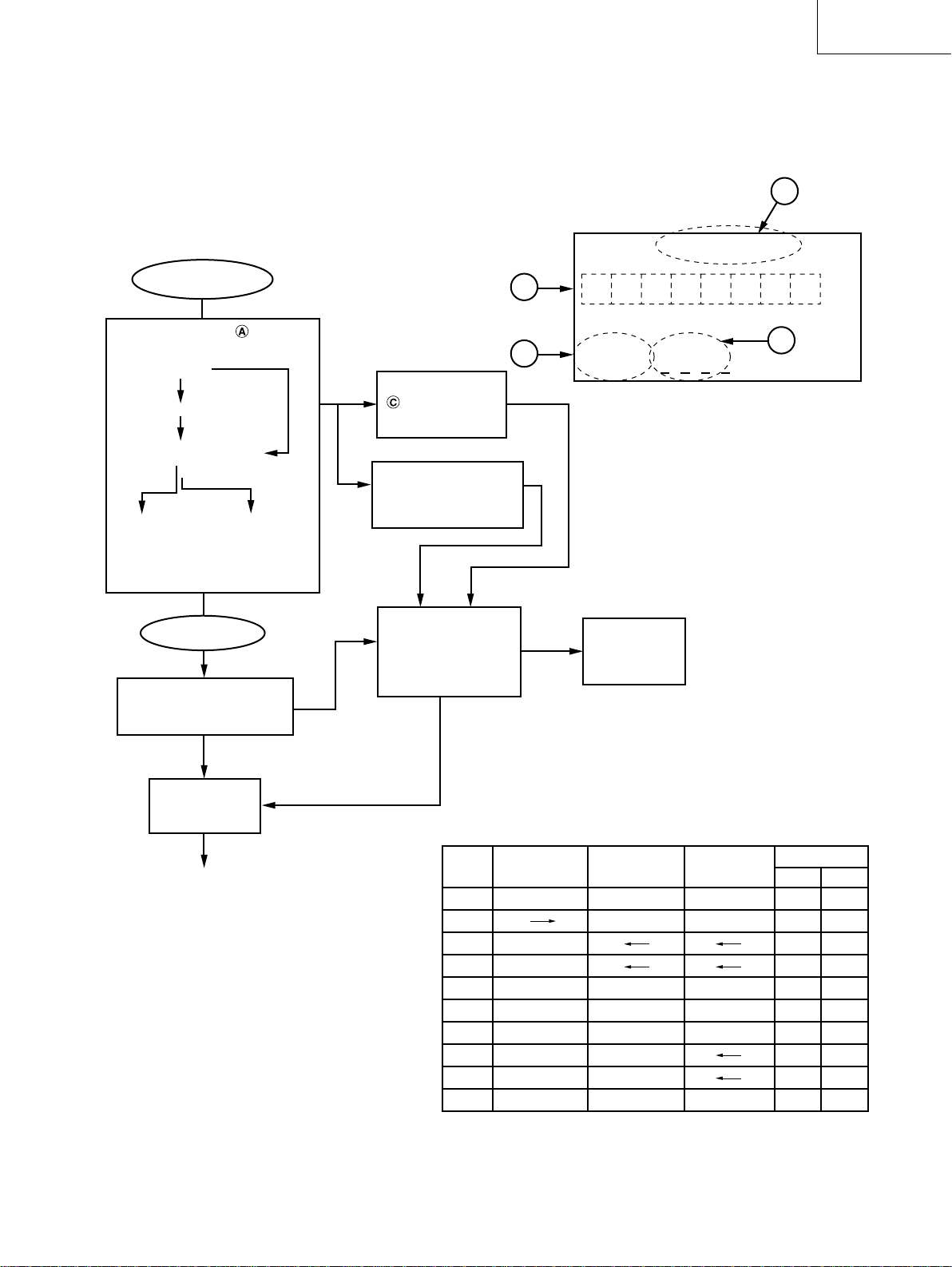
METHOD OF REMOVED IC
IC24LC194 (IC107)
When you reuse a replaced or removed IC, follow the next procedures.
1. Solder pins on the IC more as shown in the illustration.
Solders
2. Melt the solders on the pins of both sides quickly using a soldering iron until the
IC travels from the substrate. At the same time, have a tweezers on hand to pick
up the IC.
3. Pick up and remove the IC with a tweezers slowly when it travels from the
substrate. (Be careful not to delaminate the traces on the substrate.)
Tweezer
Soldering
iron
Tweezer
PWB
4. Remove and clean any redundant solders on traces on the substrate.
5. Remove the solders on leaders of the IC when you reuse it in the future.
– 36 –
Page 37

CIRCUIT DIAGRAM
TUNER/DTS Circuit
KH-WS1
— 38 —— 37 —
Page 38

KH-WS1
CIRCUIT DIAGRAM
SATELLITE Circuit
— 40 —— 39 —
Page 39

BLOCK DIAGRAM
KH-WS1
— 42 —— 41 —
Page 40

KH-WS1
EXPLODED VIEW
(Cabinet Chassis) • Nos. are reference Nos. of part list
SAT PWB
ASSY
20
10
11
13
25
15
22
17
Front Case Assembly
26
TUNER PWB
ASSY
5
18
6
27
19
33
21
3
43
42
41
12
44
Accessories
14
23
24
32
ANTENNA
PWB
PS PWB
ASSY
16
KEY PWB
ASSY
7
35
29
38
9
30
28
37
40
Back Case Assembly
8
39
34
36
31
7
— 44 —— 43 —
Page 41

THE UPDATED PARTS LIST
FOR THIS MODEL IS
AVAILABLE ON ESTA
Page 42

Hitachi, Ltd. Tokyo, Japan
International Sales Division
THE HITACHI ATAGO BUILDING,
No. 15 –12 Nishi Shinbashi, 2 – Chome,
Minato – Ku, Tokyo 105-8430, Japan.
Tel: 03 35022111
HITACHI EUROPE LTD,
Whitebrook Park
Lower Cookham Road
Maidenhead
Berkshire
SL6 8YA
UNITED KINGDOM
Tel: 01628 643000
Fax: 01628 643400
Email: consumer-service@hitachi-eu.com
HITACHI EUROPE GmbH
Munich Office
Dornacher Strasse 3
D-85622 Feldkirchen bei München
GERMANY
Tel: +49-89-991 80-0
Fax: +49- 89-991 80-224
Hotline: +49-180-551 25 51 (12ct/min)
Email: HSE-DUS.service@hitachi-eu.com
HITACHI EUROPE srl
Via Tommaso Gulli N.39, 20147
Milano, Italia
ITALY
Tel: +39 02 487861
Tel: +39 02 38073415 Servizio Clienti
Fax: +39 02 48786381/2
Email: customerservice.italy@hitachi-eu.com
HITACHI EUROPE S.A.S
Lyon Office
B.P. 45, 69671 BRON CEDEX
FRANCE
Tel: 04 72 14 29 70
Fax: 04 72 14 29 99
Email: france.consommateur@hitachi-eu.com
HITACH EUROPE AB
Egebækgård
Egebækvej 98
DK-2850 Nærum
DENMARK
Tel: +45 43 43 6050
Fax: +45 43 60 51
Email: csgnor@hitachi-eu.com
Hitachi Europe Ltd
Bergensesteenweg 421
1600 Sint- Pieters-Leeuw
BELGIUM
Tel: +32 2 363 99 01
Fax: +32 2 363 99 00
Email: sofie.van.bom@hitachi-eu.com
www.hitachidigitalmedia.com
HITACHI EUROPE S.A.
364 Kifissias Ave. & 1, Delfon Str.
152 33 Chalandri
Athens
GREECE
Tel: 1-6837200
Fax: 1-6835964
Email: service.hellas@hitachi-eu.com
HITACHI EUROPE S.A.
Gran Via Carlos III, 101- 1
08028 Barcelona
SPAIN
Tel: 93 409 2550
Fax: 93 491 3513
Email: atencion.cliente@hitachi-eu.com
HITACHI Europe AB
Box 77 S-164 94 Kista
SWEDEN
Tel: +46 (0) 8 562 711 00
Fax: +46 (0) 8 562 711 13
Email: csgswe@hitachi-eu.com
HITACHI EUROPE LTD (Norway) AB
STRANDVEIEN 18
1366 Lysaker
NORWAY
Tel: 67 5190 30
Fax: 67 5190 32
Email: csgnor@hitachi-eu.com
HITACHI EUROPE AB
Neopoli / Niemenkatu 73
FIN-15140 Lahti
FINLAND
Tel : +358 3 8858 271
Fax: +358 3 8858 272
Email: csgnor@hitachi-eu.com
HITACHI EUROPE LTD
Na Sychrove 975/8
101 27 Praha 10 – Bohdalec
CZECH REPUBLIC
Tel: +420 267 212 383
Fax: +420 267 212 385
Email: csgnor@hitachi-eu.com
 Loading...